
1
SY88843V
Micrel
M9999-030204
hbwhelp@micrel.com or (408) 955-1690
DESCRIPTION
s
Multi-rate up to 3.2Gbps operation
s
Wide gain-bandwidth product
∑ 38dB differential gain
∑ 2GHz 3dB bandwidth
s
Low noise 50
CML data outputs
∑ 800mV
pp
output swing
∑ 60ps edge rates
∑ 5ps
rms
typ. random jitter
∑ 15ps
pp
typ. deterministic jitter
s
Chatter-free, Signal-Detect (SD) output
∑ 4.6dB electrical hysteresis
∑ OC-TTL output with internal 4.75k
pull-up
resistor
s
Programmable SD sensitivity using single external
resistor
s
Internal 50
data input termination
s
TTL EN input allows feedback from SD
s
Wide operating range
∑ Single 3.3V
±
10% or 5V
±
10% power supply
∑ ≠40
∞
C to +85
∞
C industrial temperature range
s
Available in tiny 10-pin EPAD-MSOP and
16-pin MLFTM packages
FEATURES
3.3V/5V 3.2Gbps CML LOW-POWER
LIMITING POST AMPLIFIER w/TTL SD
SY88843V
The SY88843V low-power limiting post amplifier is
designed for use in fiber-optic receivers. The device connects
to typical transimpedance amplifiers (TIAs). The linear signal
output from TIAs can contain significant amounts of noise
and may vary in amplitude over time. The SY88843V
quantizes these signals and outputs typically 800mV
pp
voltage-limited waveforms.
The SY88843V operates from a single +3.3V
±
10% or
+5V
±
10% power supply, over an industrial temperature
range of ≠40
∞
C to +85
∞
C. With its wide bandwidth and high
gain, signals with data rates up to 3.2Gbps and as small as
10mVp-p can be amplified to drive devices with CML inputs
or AC-coupled PECL inputs.
The SY88843V incorporates a signal detect (SD), open-
collector TTL output with internal 4.75k
pull-up resistor. A
programmable, loss-of-signal level set pin (SDLVL) sets the
sensitivity of the input amplitude detection. SD asserts high
if the input amplitude falls below the threshold set by SDLVL
and de-asserts low otherwise. SD can be fed back to the
enable (EN) input to maintain output stability under a loss
of signal condition. EN asserts the true output signal without
removing the input signal. Typically 4.6dB SD hysteresis is
provided to prevent chattering.
Please see Micrel's website at www.micrel.com for a
complete selection of optical module ICs. The following table
summarizes the differences between devices in Micrel's
latest family of Limiting Amplifiers.
All support documentation can be found on Micrel's web
site at www.micrel.com.
Integrated 50
LOS
Active LOW
Part Number
Input Termination
or SD
or HIGH Enable
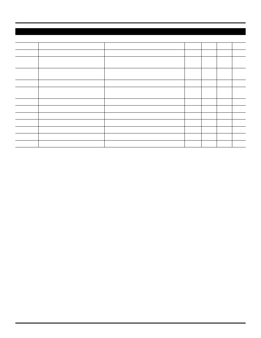
SY88773V
No
LOS
LOW
SY88823V
No
SD
HIGH
SY88843V
Yes
SD
HIGH
SY88843V
Yes
LOS
LOW
Table 1. Limiting Amplifiers Selection Guide
APPLICATIONS
s
1.25Gbps and 2.5Gbps Gigabit Ethernet
s
1.062Gbps and 2.125Gbps Fibre Channel
s
155Mbps, 622Mbps, 1.25Gbps, and 2.5Gbps SONET/
SDH
s
Gigabit interface converter (GBIC)
s
Small form factor (SFF) and small form factor
pluggable (SFP) transceivers
s
Parallel 10G Ethernet
s
High-gain line driver and line receiver
Rev.: A
Amendment: /0
Issue Date:
March 2004
Micro
LeadFrame and MLF are trademarks of Amkor Technology
TYPICAL PERFORMANCE
3.3V, 25∞C, 10mV
pp
Input
@3.2Gbps 2
31
≠1 PRBS, R
LOAD
= 50
to V
CC
TIME (50ps/div.)
Output Swing
(75mV/div
.)

2
SY88843V
Micrel
M9999-030204
hbwhelp@micrel.com or (408) 955-1690
FUNCTIONAL BLOCK DIAGRAM
Limiting
Amplifer
CML
Buffer
GND
TTL
Buffer
Level
Detect
EN
SD
DIN
/DIN
REF
SDLVL
DOUT
/DOUT
REF
Generator
OC-TTL
Buffer
50
2.8k
4.75k
VCC
VCC
25k
VCC

3
SY88843V
Micrel
M9999-030204
hbwhelp@micrel.com or (408) 955-1690
PACKAGE/ORDERING INFORMATION
1
EN
DIN
/DIN
REF
SDLVL
10 VCC
DOUT
/DOUT
SD
GND
9
8
7
6
2
3
4
5
10-Pin EPAD-MSOP (K10-2)
1
2
3
4
12
11
10
9
16 15 14 13
5
6
7
8
DIN
GND
GND
/DIN
DOUT
GND
GND
/DOUT
VCC
SDL
VL
EN
VCC
VCC
SD
REF
VCC
16-Pin MLFTM (MLF-16)
PIN DESCRIPTION
Ordering Information
Package
Operating
Package
Part Number
Type
Range
Marking
SY88843VKI
K10-2
Industrial
843V
SY88843VKITR
(1)
K10-2
Industrial
843V
SY88843VMI
MLF-16
Industrial
843V
SY88843VMITR
(1)
MLF-16
Industrial
843V
Note:
1. Tape and Reel.
Pin Number
Pin Number
(MSOP)
(MLFTM)
Pin Name
Type
Pin Function
1
15
EN
TTL Input:
Enable: De-asserts true data output when low.
Default is high.
Incorporates 25k
pull-up to VCC.
2, 3
1, 4
DIN, /DIN
Differential
Differential data input. Each pin internally terminates to
Data Input
REF through 50
.
4
6
REF
Reference Voltage: Bypass with 0.01
µ
F low ESR
capacitor from REF to VCC to stabilize SDLVL and REF.
5
14
SDLVL
Input:
Signal Detect Level Set: A resistor from this pin to VCC
Default is
sets the threshold for the data input amplitude at which
maximum sensitivity.
the SD output will be asserted.
6
2, 3, 10, 11
GND
Ground
Device ground. Exposed pad must be soldered
Exposed Pad
Exposed Pad
(or equivalent) to the same potential as the ground pins.
7
7
SD
Open Collector
Signal Detect: Asserts high when the data input amplitude
TTL Output with
rises above the threshold set by SDLVL.
internal 4.75k
pull-up resistor
8, 9
9, 12
DOUT, /DOUT
Differential
Differential data output.
CML Output
10
5, 8, 13, 16
VCC
Power Supply
Positive power supply. Bypass with 0.1
µ
F
0.01
µ
F low
ESR capacitors. 0.01
µ
F capacitors should be as close as
possible to VCC pins.

4
SY88843V
Micrel
M9999-030204
hbwhelp@micrel.com or (408) 955-1690
Absolute Maximum Ratings
(1)
Supply Voltage (V
CC
) ....................................... 0V to +7.0V
EN, SDLVL Voltage ................................................ 0 to V
CC
REF Current ...............................................................
±
1mA
SD Current .................................................................
±
5mA
DOUT, /DOUT Current .............................................
±
25mA
DIN, /DIN Current .....................................................
±
10mA
Storage Temperature (T
S
) ....................... ≠65
∞
C to +150
∞
C
Lead Temperature (Soldering, 10 sec.) .................... 265
∞
C
Operating Ratings
(2)
Supply Voltage (V
CC
) .............................. +3.0V to +3.6V or
............................................................ +4.5V to +5.5V
Ambient Temperature (T
A
) ......................... ≠40
∞
C to +85
∞
C
Junction Temperature (T
J
) ....................... ≠40
∞
C to +120
∞
C
Package Thermal Resistance
(3)
MLFTM
JA
(Still-Air) ..................................................... 61
∞
C/W
JB ...................................................................................
38
∞
C/W
EPAD-MSOP
JA
(Still-Air) ..................................................... 38
∞
C/W
JB ...................................................................................
22
∞
C/W
V
CC
= 3.0V to 3.6V or 4.5V to 5.5V, T
A
= ≠40
∞
C to +85
∞
C; typical values at V
CC
= 3.3V, T
A
= 25
∞
C
Symbol
Parameter
Condition
Min
Typ
Max
Units
I
CC
Power Supply Current
3.3V, Note 4
28
42
mA
5V, Note 4
30
45
mA
Power Supply Current
3.3V, Note 5
45
62
mA
5V, Note 5
47
65
mA
V
REF
REF Voltage
V
CC
≠1.3
V
SDLVL
SDLVL
Voltage Range
V
REF
V
CC
V
V
OH
DOUT, /DOUT HIGH Voltage
Note 6
V
CC
≠0.020 V
CC
≠0.005
V
CC
V
V
OL
DOUT, /DOUT LOW Voltage
3.3V, Note 6
V
CC
≠0.475 V
CC
≠0.400 V
CC
≠0.350
V
5V, Note 6
V
CC
≠0.510 V
CC
≠0.400 V
CC
≠0.350
V
V
OFFSET
Differential Output Offset
Note 6
±
80
mV
Z
O
Single-Ended Output Impedance
40
50
60
Z
I
Single-Ended Input Impedance
40
50
60
DC ELECTRICAL CHARACTERISTICS
V
CC
= 3.0V to 3.6V or 4.5V to 5.5V, T
A
= ≠40
∞
C to +85
∞
C
Symbol
Parameter
Condition
Min
Typ
Max
Units
V
OH
SD Output HIGH Level
Sourcing 100
µ
A
2.4
V
CC
V
V
OL
SD Output LOW Level
Sinking 2mA
0.5
V
V
IH
EN Input HIGH Voltage
2.0
V
V
IL
EN Input LOW Voltage
0.8
V
I
IH
EN Input HIGH Current
V
IN
= 2.7V
20
µ
A
V
IN
= V
CC
100
µ
A
I
IL
EN Input LOW Current
V
IN
= 0.5V
≠0.3
mA
Notes:
1. Permanent device damage may occur if Absolute Maximum Ratings are exceeded. This is a stress rating only and functional operation is not implied
at conditions other than those detailed in the operational sections of this data sheet. Exposure to Absolute Maximum Rating conditions for extended
periods may affect device reliability.
2. The data sheet limits are not guaranteed if the device is operated beyond the operating ratings.
3. Thermal performance assumes the use of 4-layer PCB. Exposed pad must be soldered (or equivalent) to the device's most negative potential on the
PCB.
4. Excludes current of CML output stage. See "Detailed Description."
5. Total device current with no output load.
6. Output levels are based on a 50
to V
CC
load impedance. If the load impedance is different, the output level will be changed. Amplifier is in limiting
mode.
TTL DC ELECTRICAL CHARACTERISTICS
5
SY88843V
Micrel
M9999-030204
hbwhelp@micrel.com or (408) 955-1690
V
CC
= 3.0V to 3.6V or 4.5V to 5.5V, T
A
= ≠40
∞
C to +85
∞
C, R
LOAD
= 50
to V
CC
; typical values at V
CC
= 3.3V, T
A
= 25
∞
C.
Symbol
Parameter
Condition
Min
Typ
Max
Units
PSRR
Power Supply Rejection Ratio
35
dB
t
r
,t
f
Output Rise/Fall Time
Note 7
60
120
ps
(20% to 80%)
t
JITTER
Deterministic
Note 8
15
ps
pp
Random
5
ps
rms
V
ID
Differential Input Voltage Swing
10
1800
mV
pp
V
OD
Differential Output Voltage Swing
3.3V, Note 7
700
800
950
mV
pp
5V, Note 7
700
800
1020
mV
pp
HYS
SD Hysteresis
Note 9
2
4.6
8
dB
t
OFF
SD Release Time
0.1
0.5
µ
s
t
ON
SD Assert Time
0.2
0.5
µ
s
V
SR
SD Sensitivity Range
Note 10
10
35
mV
pp
B
≠3dB
≠3dB Bandwidth
2.0
GHz
A
V(Diff)
Differential Voltage Gain
32
38
dB
S
21
Single-Ended Small-Signal Gain
26
32
dB
Notes:
7. Amplifier in limiting mode. Input is a 200MHz square wave, t
r
< 300ps.
8. Deterministic jitter measured using 2.488Gbps K28.5 pattern, V
ID
= 10mV
pp
. Random jitter measured using 2.488Gbps K28.7 pattern, V
ID
= 10mV
pp
.
9. Electrical signal.
10. This is the detectable range of input amplitudes that can de-assert SD. The input amplitude to assert SD is 2≠8dB higher than the de-assert
amplitude. See "Typical Operating Characteristics" for graphs showing how to choose a particular V
SDLVL
or R
SDLVL
for a particular SD de-assert,
and its associated assert, amplitude. If increased SD sensitivity and hysteresis are required, an application note entitled "Notes on Sensitivity and
Hysteresis in Micrel Post Amplifiers" is available at http://www.micrel.com/product-info/app_hints+notes.shtml.
AC ELECTRICAL CHARACTERISTICS