 | –≠–ª–µ–∫—Ç—Ä–æ–Ω–Ω—ã–π –∫–æ–º–ø–æ–Ω–µ–Ω—Ç: SY88992 | –°–∫–∞—á–∞—Ç—å:  PDF PDF  ZIP ZIP |
SY88992L
3.3V, 4.25Gbps VCSEL Driver
January 2006
M9999-011306-A
hbwhelp@micrel.com
or (408) 955-1690
General Description
The SY88992L is a single supply 3.3V, low power
consumption, small-form factor VCSEL driver ideal
for use in datacom applications; Ethernet, GbE
(Gigabit Ethernet), and FC (Fibre Channel)
applications that operate from 100Mbps up to
4.25Gbps. The modulation current is set by applying
an external voltage at the IM_SET pin. The driver
features an adjustable peaking option with variable
amplitude and duration to improve VCSEL edge
response. The driver can deliver modulation current
up to 25mA and a peaking current up to 35% of the
modulation current. This device is intended to be
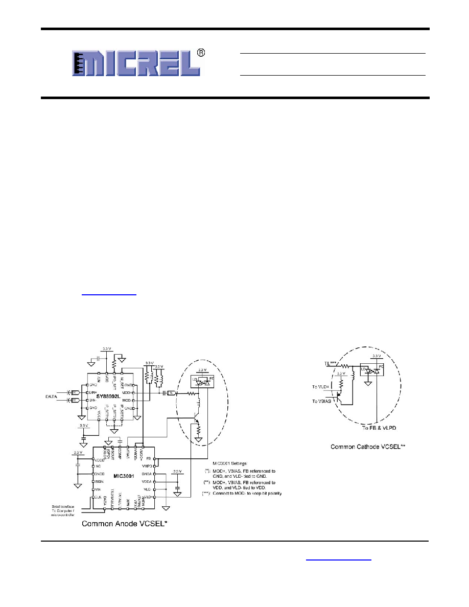
used with Micrel's MIC3001 Optical Transceiver
Management IC, which allows for both modulation
and bias current control and monitoring, APC
(Automatic Power Control), and temperature
compensation.
All support documentation can be found on Micrel's
web site at:
www.micrel.com
.
Features
∑ Up to 25mA modulation current
∑ Operates from 100Mbps to 4.25Gbps
∑ Peaking with variable duration option for better
VCSEL response.
∑ Dual peaking, on the rise and falling edges
∑ Peaking current proportional to modulation current
∑ Easy modulation current setting
∑ Fully controllable with Micrel MIC3001
∑ Small (3mm x 3mm) 16 pin MLFTM package
Applications
∑ Multirate LAN, SAN applications up to 4.25Gbps:
Ethernet, GbE, FC
∑ SFF, SFP Modules
Markets
∑ Datacom
________________________________________________________________
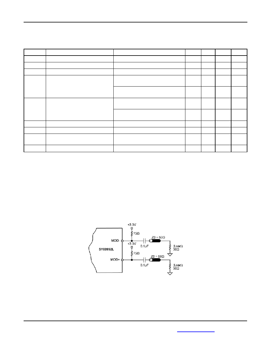
Typical Application
Micrel, Inc.
SY88992L
January 2006
2
M9999-011306-A
hbwhelp@micrel.com
or (408) 955-1690
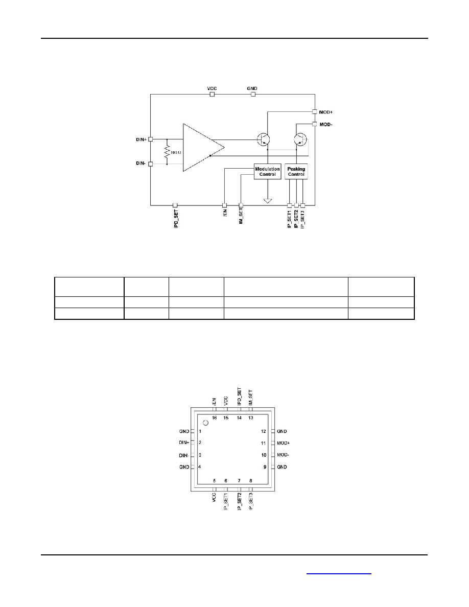
Functional Block Diagram
Ordering Information
(1)
Part Number
Package
Type
Operating
Range
Package Marking
Lead Finish
SY88992LMG
MLF-16
Industrial
992L with Pb-Free bar-line indicator
NiPdAu Pb-Free
SY88992LMGTR
(2)
MLF-16
Industrial
992L with Pb-Free bar-line indicator
NiPdAu Pb-Free
Notes:
1. Contact factory for die availability. Dice are guaranteed at T
A
= +25∞C, DC Electricals only.
2. Tape and Reel.
Pin Configuration
16-Pin MLF
TM
(MLF-16)
Micrel, Inc.
SY88992L
January 2006
3
M9999-011306-A
hbwhelp@micrel.com
or (408) 955-1690
Pin Description
Pin Number
Pin Name
Pin Function
2
DIN+
Non-Inverting Input Data. Internally terminated with 50 to a reference voltage.
3
DIN-
Inverting Input Data. Internally terminated with 50 to a reference voltage.
6
IP_SET1
Peaking Current Setting. Connect this pin to GND and keep pins 7 and 8 open to set
peaking-to-modulation current ratio to 5%. Combinations of the three pins, as shown
in table below, will set different ratios up to 35%.
7
IP_SET2
Peaking Current Setting. Connect this pin to GND and keep pins 6 and 8 open to set
peaking-to-modulation current ratio to 10%. Combinations of the three pins, as shown
in table below, will set different ratios up to 35%.
8
IP_SET3
Peaking Current Setting. Connect this pin to GND and keep pins 6 and 7 open to set
peaking-to-modulation current ratio to 20%. Combinations of the three pins, as shown
in table below, will set different ratios up to 35%.
10
MOD-
Inverted Modulation Current Output. Provides modulation current when input data is
negative.
11
MOD+
Non-Inverted Modulation Current Output. Provides modulation current when input
data is positive.
13
IM_SET
Modulation Current Setting. The modulation current is set by applying a 0V to 1.2V
voltage at this pin.
14
IPD_SET
Peaking Duration Setting. The peaking current duration is set by installing a resistor
between this pin and ground. The plot on page 6 shows peaking duration versus the
value of the resistor installed.
16
/EN
A low level signal applied to this pin will enable the output stage of the driver.
Internally pulled down to ground with 75k resistor.
1, 4, 9, 12
GND
Ground. Ground and exposed pad must be connected to the plane of the most
negative potential.
5, 15
VCC
Supply Voltage. Bypass with a 0.1µF//0.01µF low ESR capacitor as close to VCC pin
as possible.
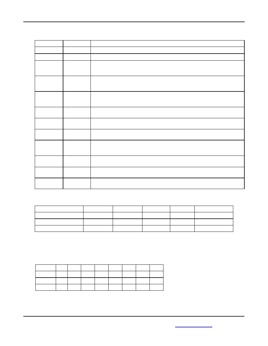
Truth Table
DIN+
DIN-
/EN
MOD+
(1)
MOD-
VCSEL Output
(2)
L
H
L
H
L
L
H
L
L
L
H
H
X
X
H
H
H
L
Notes:
1. I
MOD
= 0 when MOD+ = H.
2. Assuming a common anode VCSEL with its cathode tied to MOD+.
Peaking Current-to-Modulation Current Ratio Setting
IP/I
MOD
0 %
5 %
10 %
15 %
20 %
25 %
30 %
35 %
IP_SET1
NC
GND
NC
GND
NC
GND
NC
GND
IP_SET2
NC
NC
GND
GND
NC
NC
GND
GND
IP_SET3
NC
NC
NC
NC
GND
GND
GND
GND
Micrel, Inc.
SY88992L
January 2006
4
M9999-011306-A
hbwhelp@micrel.com
or (408) 955-1690
Absolute Maximum Ratings
(1)
Supply Voltage (V
IN
) ............................. ≠0.5V to +4.0V
CML Input Voltage (V
IN
)............ V
CC
≠1.2V to V
CC
+0.5V
TTL Control Input Voltage (V
IN
)..................... 0V to V
CC
Lead Temperature (soldering, 20sec.)............. +260∞C
Storage Temperature (T
s
) .................≠65∞C to +150∞C
Operating Ratings
(2)
Supply Voltage (V
CC
) ............................ +3.0V to +3.6V
Ambient Temperature (T
A
) .................. ≠40∞C to +85∞C
Package Thermal Resistance
(3)
MLFTM
(
JA
) Still-air ................................................ 60∞C/W
(
JB
)............................................................ 33∞C/W
DC Electrical Characteristics
T
A
= -40∞C to 85∞C and V
CC
= 3.0V to 3.6V, unless otherwise noted. Typical values are at: V
CC
= 3.3V, T
A
= 25∞C,
I
MOD
= 13mA
(4)
Symbol
Parameter
Condition
Min
Typ
Max
Units
Peaking not used
57
95
mA
I
CC
Power Supply Current
Maximum peaking used
70
110
mA
I
MOD
(4)
Modulation Current
AC-coupled
3
25
mA
I
MOD_OFF
Modulation OFF Current
Current at MOD+ and MOD- when
the part is disabled
100
µA
V
MOD_MIN
Minimum Voltage required at the
driver output (headroom) for proper
operation
1.5
V
R
IN
Input Resistance (DIN+-to-DIN-)
90
100
110
V
ID
Differential Input Voltage Swing
200
2400
mV
PP
VI
M_SET
Voltage Range on I
M_SET
I
MOD
range 3mA ≠ 25mA
(4)
1.2
V
V
IL
/EN Input Low
0.8
V
V
IH
/EN Input High
2
V
Input Impedance at /EN
75
k
Notes:
1. Permanent device damage may occur if absolute maximum ratings are exceeded. This is a stress rating only and functional operation is
not implied at conditions other than those detailed in the operational sections of this data sheet. Exposure to absolute maximum ratings
conditions for extended periods may affect device reliability.
2. The data sheet limits are not guaranteed if the device is operated beyond the operating ratings.
3. Package Thermal Resistance assumes exposed pad is soldered (or equivalent) to the devices most negative potential on the PCB.
JB
uses a 4-layer and
JA
in still air unless otherwise stated.
4. I
MOD
is defined as the current at the output of the driver. That current splits between the pull-up network at the output and the VCSEL. For a
nominal pull-up resistor of 75 at the output of the driver and a nominal 50 VCSEL equivalent resistor, 60% of that current goes to the
VCSEL.
Micrel, Inc.
SY88992L
January 2006
5
M9999-011306-A
hbwhelp@micrel.com
or (408) 955-1690
AC Electrical Characteristics
T
A
= -40∞C to +80∞C and V
CC
= 3.0 to 3.6V, unless otherwise noted. Typical values are at V
CC
= 3.3V, T
A
= 25∞C,
I
MOD
= 13mA
(5)
, and AC-coupled 50 load to ground with 75 pull-up (see Figure below).
Symbol
Parameter
Condition
Min
Typ
Max
Units
Data Rate
NRZ
0.1
4.25
Gbps
t
OFF
(6)
Turn OFF Time
50 load
1
1.5
ns
t
ON
(7)
Turn ON Time
50 load
1.8
2.5
ns
20% to 80%, I
MOD
= 13mA, no
peaking, 50 load
65
95
ps
t
r
Output Current Rise Time
20% to 80%, I
MOD
= 13mA,
I
P
/I
MOD
=20%, R
IPD
=1.5k
60
75
ps
20% to 80%, I
MOD
= 13mA, no
peaking, 50 load
65
95
ps
t
f
Output Current Fall Time
20% to 80%, I
MOD
= 13mA,
I
P
/I
MOD
=20%, R
IPD
=1.5k
60
75
ps
Total Jitter
@ 2.5Gbps data rate, 50 load
30
ps
PP
Pulse-Width Distortion
50 load
20
ps
(I
P
/ I
MOD
)
Max
Maximum Peaking Current-to-
Modulation Current Ratio
35
%
t
P
Peaking Current Duration
(8)
I
MOD
= 13mA, R
IPD_SET
= 0
150
ps
Notes:
5. I
MOD
is defined as the current at the output of the driver. That current splits between the pull-up network at the output and the VCSEL. For a
nominal pull-up resistor of 75 at the output of the driver and a nominal 50 VCSEL equivalent resistor, 60% of that current goes to the
VCSEL.
6. Turn-OFF time is defined as the delay between the time the signal at /EN rises to 50% of its amplitude and the time when the output of the
driver reaches 10% of its steady-state amplitude.
7. Turn-ON time is defined as the delay between the time the signal at /EN falls to 50% of its amplitude and the time when the output of the
driver reaches 90% of its steady-state amplitude.
8. The peaking current duration is the time between the start of the peaking current, which is the same as the start of the modulation current
transition, and the time when the peaking current reaches its maximum, i.e., the top of the peak.
Test Circuit