1
Precision EdgeTM
SY89295U
Micrel
M9999-031604
hbwhelp@micrel.com or (408) 955-1690
DESCRIPTION
s
Precision LVPECL programmable delay line
s
Guaranteed AC performance over temperature and
voltage:
∑ > 1.5GHz f
MAX
∑ < 160ps rise/fall times
s
Low-jitter design:
∑ < 10ps
pp
total jitter
∑ < 2ps
rms
cycle-to-cycle jitter
∑ < 1ps
rms
random jitter
s
Programmable delay range: 3.2ns to 14.8ns in 10ps
increments
s
Increased monotonicity over the MIC100EP195
s
±
10% of LSB INL
s
V
BB
output reference voltage
s
Parallel inputs accepts LVPECL or CMOS/LVTTL
s
Low voltage operation: 2.5V
±
5% and 3.3V
±
10%
s
Industrial ≠40
∞
C to +85
∞
C temperature range
s
Available in 32-pin (5mm
◊◊
◊◊
◊
5mm) MLFTM and 32-pin
TQFP packages
FEATURES
2.5V/3.3V 1.5GHz PRECISION
LVPECL PROGRAMMABLE DELAY
Precision EdgeTM
SY89295U
APPLICATIONS
s
Clock de-skewing
s
Timing adjustments
s
Aperture centering
Rev.: A
Amendment: /0
Issue Date:
March 2004
The SY89295U is a programmable delay line that delays
the input signal using a digital control signal. The delay can
vary from 3.2ns to 14.8ns in 10ps increments. In addition,
the input signal is LVPECL, uses either a 2.5V
±
5% or 3.3V
±
10% power supply, and is guaranteed over the full industrial
temperature range (≠40
∞
C to +85
∞
C).
The delay varies in discrete steps based on a control
word. The control word is 10-bits long and controls the
delay in 10ps increments. The eleventh bit is D[10] and is
used to simultaneously cascade the SY89295U which allows
for a larger delay range. In addition, the input pins IN and
/IN default to an equivalent low state when left floating.
Further, for maximum flexibility, the control register interface
accepts CMOS or TTL level signals.
For applications that requires an analog delay input, see
the SY89296L which is a programmable delay chip with
fine tune control. The SY89295U and SY89296U are part
of Micrel's high-speed, Precision EdgeTM product line.
All support documentation can be found on Micrel's
website at www.micrel.com.
Precision Edge is a trademark of Micrel, Inc.
Micro
LeadFrame and MLF are trademarks of Amkor Technology, Inc.
Precision EdgeTM
2
Precision EdgeTM
SY89295U
Micrel
M9999-031604
hbwhelp@micrel.com or (408) 955-1690
PACKAGE/ORDERING INFORMATION
Ordering Information
(1)
Package
Operating
Package
Part Number
Type
Range
Marking
SY89295UMI
MLF-32
Industrial
SY89295U
SY89295UMITR
(2)
MLF-32
Industrial
SY89295U
SY89295UTI
T32-1
Industrial
SY89295U
SY89295UTITR
(2)
T32-1
Industrial
SY89295U
Notes:
1. Contact factory for die availability. Dice are guaranteed at T
A
= 25
∞
C,
DC electricals only.
2. Tape and Reel.
1
2
3
4
5
6
7
8
24
23
22
21
20
19
18
17
9 10 11 12 13 14 15 16
32 3130 29 28 27 26 25
D8
D9
D10
IN
/IN
VBB
VEF
VCF
GND
D0
VCC
Q
/Q
VCC
VCC
NC
GND
D4
D5
D6
D7
D3
D2
D1
VCC
SETMAX
SETMIN
LEN
GND
/CASCADE
CASCADE
/EN
32-Pin MLFTM (MLF-32)
GND
D4
D5
D6
D7
D3
D2
D1
VCC
SETMAX
SETMIN
LEN
GND
/
CASCADE
CASCADE
/EN
GND
D0
VCC
Q
/Q
VCC
VCC
NC
D8
D9
D10
IN
/IN
VBB
VEF
VCF
32 31 30 29 28 27 26 25
9 10 11 12 13 14 15 16
1
2
3
4
5
6
7
8
24
23
22
21
20
19
18
17
32-Pin TQFP (T32-1)
TRUTH TABLES
Input Enable
/EN
Q, /Q
0
IN, /IN Delayed
1
Latched D[10:0]
Digital Control Latch
LEN
Latch Action
0
Pass Through D[10:0]
1
Latched D[10:0]
Input/Output
Inputs
Outputs
IN
/IN
OUT
/OUT
0
1
0
1
1
0
1
0
3
Precision EdgeTM
SY89295U
Micrel
M9999-031604
hbwhelp@micrel.com or (408) 955-1690
FUNCTIONAL BLOCK DIAGRAM
512
GD
0
1
256
GD
0
1
128
GD
0
1
64
GD
0
1
32
GD
0
1
16
GD
D[9:0]
LEN
IN
/IN
/EN
SETMIN
SETMAX
D[10]
0
1
8
GD
0
1
4
GD
0
1
2
GD
0
1
1
GD
0
1
1
GD
Q
/Q
0
1
CASCADE
/CASCADE
10-bit
Latch
Latch
V
BB
V
CF
V
EF
4
Precision EdgeTM
SY89295U
Micrel
M9999-031604
hbwhelp@micrel.com or (408) 955-1690
Pin Number
Pin Name
Pin Function
23, 25, 26, 27, 29,
D[9:0]
CMOS, ECL, or TTL Control Bits: These control signals adjust the delay from IN to Q.
30, 31, 32, 1, 2
See "AC Electrical Characteristics" for delay values. In addition, see "Interface Applications"
section which illustrates the proper interfacing techniques for different logic standards.
D[9:0] contains pull-downs and defaults LOW when left floating. D0 (LSB), and D9 (MSB).
See "Typical Operating Characteristics" for delay information.
3
D10
CMOS, ECL, or TTL Control Bit: This bit is used to cascade devices for an extended delay
range. In addition, it drives CASCADE, and /CASCADE. Further, D[10] contains a pull-
down and defaults LOW when left floating.
4, 5
IN, /IN
LVPECL/ECL Signal Input: Input signal to be delayed. IN contains a 75k
pull-down and
will default to a logic LOW if left floating.
6
VBB
(1)
Reference Voltage Output: When using a single-ended input signal source to IN or /IN,
connect the unused input of the differential pair to this pin. This pin can also be used to
rebias AC-coupled inputs to IN and /IN. When used, de-couple to V
CC
using a 0.01
µ
F
capacitor, otherwise leave floating if not used. Maximum sink/source is
±
0.5mA.
7
VEF
Reference Voltage Output: Connect this pin to V
CF
when D[9:0], and D[10] is ECL.
8
VCF
Reference Voltage Input: The voltage driven on V
CF
sets the logic transition threshold for
D[9:0], and D[10].
9, 24, 28
GND,
Negative Supply: For MLFTM package, exposed pad must be connected to a ground plane
Exposed Pad
(2)
that is the same potential as the ground pin.
10
LEN
ECL Control Input: When HIGH latches the D[9:0] and D[10] bits. When LOW, the D[9:0]
and D[10] latches are transparent.
11
SETMIN
ECL Control Input: When HIGH, D[9:0] registers are reset. When LOW, the delay is set
by SETMAX or D[9:0] and D[10]. SETMIN contains a pull-down and defaults LOW when
left floating.
12
SETMAX
ECL Control Input: When SETMAX is set HIGH and SETMIN is set LOW, D[9:0] =
10'b1111111111. When SETMAX is LOW, the delay is set by SETMIN or D[9:0] and
D[10]. SETMAX contains a pull-down and defaults LOW when left floating.
13, 18, 19, 22
VCC
Positive Power Supply: Bypass with 0.1
µ
F and 0.01
µ
F low ESR capacitors.
14, 15
/Cascade,
LVPECL Differential Output: The outputs are used when cascading two or more
Cascade
SY89295U to extend the delay range.
16
/EN
LVPECL Single-Ended Control Input: When LOW, Q is delayed from IN. When HIGH,
Q is a differential LOW. /EN contains a pull-down and defaults LOW when left floating.
20, 21
/Q, Q
LVPECL Differential Output: Q is a delayed version of IN. Always terminate the
output with 50
to V
CC
≠ 2V. See "Output Interface Applications" section.
17
NC
No Connect.
Notes:
1. Single-ended operation is only functional at 3.3V.
2. MLFTM package only.
PIN DESCRIPTION
Logic Standard
V
CF
Connects to
LVPECL
V
EF
,
(1)
CMOS
No Connect
TTL
1.5V Source
5
Precision EdgeTM
SY89295U
Micrel
M9999-031604
hbwhelp@micrel.com or (408) 955-1690
Absolute Maximum Ratings
(1)
Supply Voltage (V
CC
) .................................. ≠0.5V to +4.0V
Input Voltage (V
IN
) ......................................... ≠0.5V to V
CC
LVPECL Output Current (I
OUT
)
Continuous ......................................................... 50mA
Surge ................................................................ 100mA
Lead Temperature (soldering, 10 sec.) ................... +220
∞
C
Storage Temperature Range (T
S
) ............ ≠65
∞
C to +150
∞
C
Operating Ratings
(2)
Supply Voltage (V
CC
) .............................. +2.375V to +3.6V
Ambient Temperature (T
A
) ......................... ≠40
∞
C to +85
∞
C
Package Thermal Resistance
(3)
MLFTM
(
JA
)
Still-Air ............................................................. 35
∞
C/W
MLFTM
(
JB
)
Junction-to-Board ............................................ 28
∞
C/W
TQFP
(
JA
)
Still-Air ............................................................. 28
∞
C/W
TQFP
(
JB
)
Junction-to-Board ............................................ 20
∞
C/W
T
A
= ≠40
∞
C to 85
∞
C, unless otherwise stated.
Symbol
Parameter
Condition
Min
Typ
Max
Units
V
CC
Power Supply
V
CC
= 2.5V
2.375
2.5
2.625
V
V
CC
= 3.3V
3
3.3
3.6
V
I
EE
Power Supply Current
No load, max V
CC
220
mA
V
IN
Input Voltage Swing (IN, /IN)
See Figure 1a.
150
1200
mV
V
DIFF_IN
Differential Input Voltage
See Figure 1b.
300
2400
mV
Swing (IN, /IN)
V
IHCMR
Input High Common Mode Range
IN, I
NB
V
EE
+1.2
V
CC
V
DC ELECTRICAL CHARACTERISTICS
(4)
V
CC
= 3.3V, T
A
= ≠40
∞
C to 85
∞
C, unless otherwise stated.
Symbol
Parameter
Condition
Min
Typ
Max
Units
V
IH
Input High Voltage (IN, /IN)
2.075
2.420
V
V
IL
Input Low High Voltage (IN, /IN)
1.355
1.675
V
V
BB
Output Voltage Reference
Ground Reference
1.325
1.425
1.525
V
V
EF
Mode Connection
Ground Reference
1.20
1.30
1.4
V
V
CF
Input Select Voltage
1.55
1.65
1.75
V
V
CC
= 2.5V, T
A
= ≠40
∞
C to 85
∞
C, unless otherwise stated.
Symbol
Parameter
Condition
Min
Typ
Max
Units
V
IH
Input High Voltage (IN, /IN)
2.075
2.42
V
V
IL
Input Low High Voltage (IN, /IN)
1.355
1.675
V
V
BB
Output Voltage Reference
Ground Reference
1.325
1.425
1.525
V
V
EF
Mode Connection
Ground Reference
1.20
1.30
1.40
V
V
CF
Input Select Voltage
1.15
1.25
1.35
V
Notes:
1. Permanent device damage may occur if the ratings in the "Absolute Maximum Ratings" section are exceeded. This is a stress rating only and
functional operation is not implied at conditions other than those detailed in the operational sections of this data sheet. Exposure to absolute
maximum ratings for extended periods may affect device reliability.
2. The data sheet limits are not guaranteed if the device is operated beyond the operating ratings.
3. Thermal performance on MLFTM packages assumes exposed pad is soldered (or equivalent) to the device most negative potential (GND).
4. The circuit is designed to meet the DC specifications shown in the table above after thermal equilibrium has been established. Input and output
parameters vary 1:1 with V
CC
.
6
6
Precision EdgeTM
SY89295U
Micrel
M9999-031604
hbwhelp@micrel.com or (408) 955-1690
V
CC
= 2.5V
±
5% or 3.3V
±
10%; R
LOAD
= 50
to V
CC
≠2V; T
A
= ≠40
∞
C to +85
∞
C, unless otherwise stated.
Symbol
Parameter
Condition
Min
Typ
Max
Units
V
OH
Output HIGH Voltage (Q, /Q)
2.155
2.280
2.405
V
V
OL
Output LOW Voltage (Q, /Q)
1.355
1.480
1.605
V
V
OUT
Output Voltage Swing (Q, /Q)
See Figure 1a.
550
800
mV
V
DIFF_OUT
Differential Output Voltage Swing
See Figure 1b.
1.1
1.6
V
(Q, /Q)
LVPECL OUTPUTS DC ELECTRICAL CHARACTERISTICS
(5)
V
CC
= 2.5V
±
5% or 3.3V
±
10%; T
A
= ≠40
∞
C to +85
∞
C, unless otherwise stated.
Symbol
Parameter
Condition
Min
Typ
Max
Units
V
IH
Input HIGH Voltage
2.0
V
V
IL
Input LOW Voltage
0.8
V
I
IH
Input HIGH Current
40
µ
A
I
IL
Input LOW Current
-300
µ
A
Notes:
5. The circuit is designed to meet the DC specifications shown in the table above after thermal equilibrium has been established. All input and output
parameters vary 1:1 with V
CC
, however, the values are referenced to 3.3V.
6. The circuit is designed to meet the DC specifications shown in the table above after thermal equilibrium has been established.
LVTTL/CMOS DC ELECTRICAL CHARACTERISTICS
(6)
7
Precision EdgeTM
SY89295U
Micrel
M9999-031604
hbwhelp@micrel.com or (408) 955-1690
T
A
= ≠40
∞
C to +85
∞
C; unless otherwise stated.
Symbol
Parameter
Condition
Min
Typ
Max
Units
f
MAX
Maximum Operating Frequency
Clock V
OUT
400mV
1.5
GHz
t
pd
Propagation Delay
IN to Q; D[0≠10]=0
3200
4200
ps
IN to Q; D[0≠10]=1023
11500
14800
ps
/EN to Q: D[0≠10]=0
3400
4400
ps
D10 to CASCADE
350
670
ps
t
RANGE
Programmable Range
t
pd
(max) ≠ t
pd
(min)
8300
ps
t
SKEW
Duty Cycle Skew
Note 8
25
ps
t
Step Delay
D0 High
10
ps
D1 High
15
ps
D2 High
35
ps
D3 High
70
ps
D4 High
145
ps
D5 High
290
ps
D6 High
575
ps
D7 High
1150
ps
D8 High
2300
ps
D9 High
4610
ps
D0-D9 High
9220
ps
INL
Integral Non-Linearity
Note 9
≠10
+10
%LSB
t
S
Setup Time
D to LEN
200
ps
D to IN
Note 10
350
ps
/EN to IN
Note 11
300
ps
t
H
Hold Time
LEN to D
200
ps
IN to /EN
Note 12
400
ps
t
R
Release Time
/EN to IN
500
ps
SETMAX to LEN
500
ps
SETMIN to LEN
450
ps
t
JITTER
Cycle-to-Cycle Jitter
Note 13
2
ps
rms
Total Jitter
Note 14
10
ps
p-p
Random Jitter
Note 15
1
ps
rms
t
r
, t
f
Output Rise/Fall Time
20% to 80% (Q)
50
85
160
ps
20% to 80% (CASCADE)
90
300
ps
Duty Cycle
45
55
%
Notes:
7. High frequency AC electricals are guaranteed by design and characterization.
8. Duty cycle skew guaranteed only for differential operation measured from the cross point of the input to the crosspoint of the output.
9. INL (Integral Non-Linearity) is defined from its corresponding point on the ideal delay versus D[9:0] curve as the deviation from its ideal delay. The
maximum difference is the INL. Theoretical Ideal Linearity (TIL) = (measured maximum delay ≠ measured minimum delay)
˜
1024. INL = measured
delay ≠ measured minimum delay + (step number
◊
TIL).
10. This setup time defines the amount of time prior to the input signal. The delay tap of the device must be set.
11. This setup time defines the amount of the time that /EN must be asserted prior to the next transition of IN, /IN to prevent an output response greater
than
±
75mV to the IN, /IN transition.
12. Hold time is the minimum time that /EN must remain asserted after a negative going IN or a positive going /IN to prevent an output response greater
than
±
75mV to the IN, /IN transition.
13. Cycle-to-cycle jitter definition: The variation of periods between adjacent cycles over a random sample of adjacent cycle pairs.
T
jitter_cc
= T
n
≠ T
n
+1, where T is the time between rising edges of the output signal.
14. Total jitter definition: With an ideal clock input, no more than one output edge in 10
12
output edges will deviate by more than the specified peak-to-
peak jitter value.
15. Random jitter definition: Jitter that is characterized by a Gaussian distribution, unbounded and is quantified by its standard deviation and mean.
Random jitter is measured with a K28.7 comma defect pattern, measured at 1.5Gbps.
AC ELECTRICAL CHARACTERISTICS
(7)
8
Precision EdgeTM
SY89295U
Micrel
M9999-031604
hbwhelp@micrel.com or (408) 955-1690
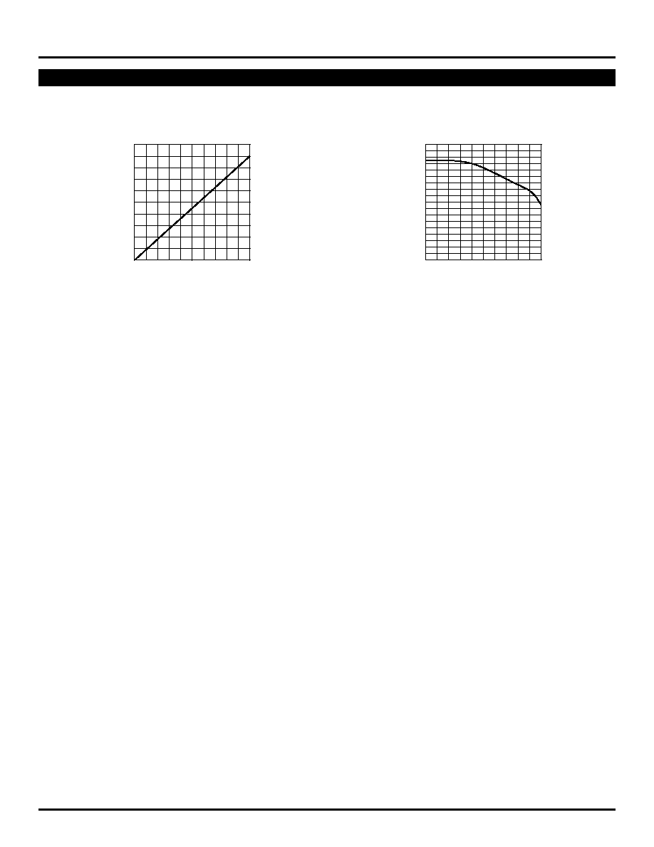
TYPICAL OPERATING CHARACTERISTICS
0
1000
2000
3000
4000
5000
6000
7000
8000
9000
10000
0
500
1000
DELAY (ps)
D[9:0]
Delay vs. D[9:0]
0
100
200
300
400
500
600
700
800
900
0
500
1000 1500 2000 2500
AMPLITUDE (mV)
FREQUENCY (MHz)
Amplitude vs. Frequency
V
CC
= 3.3V, GND = 0, D
IN
= 100mV, T
A
= 25
∞
C, unless otherwise stated.
9
Precision EdgeTM
SY89295U
Micrel
M9999-031604
hbwhelp@micrel.com or (408) 955-1690
TIMING DIAGRAM
/IN
IN
/Q
Q
t
pd
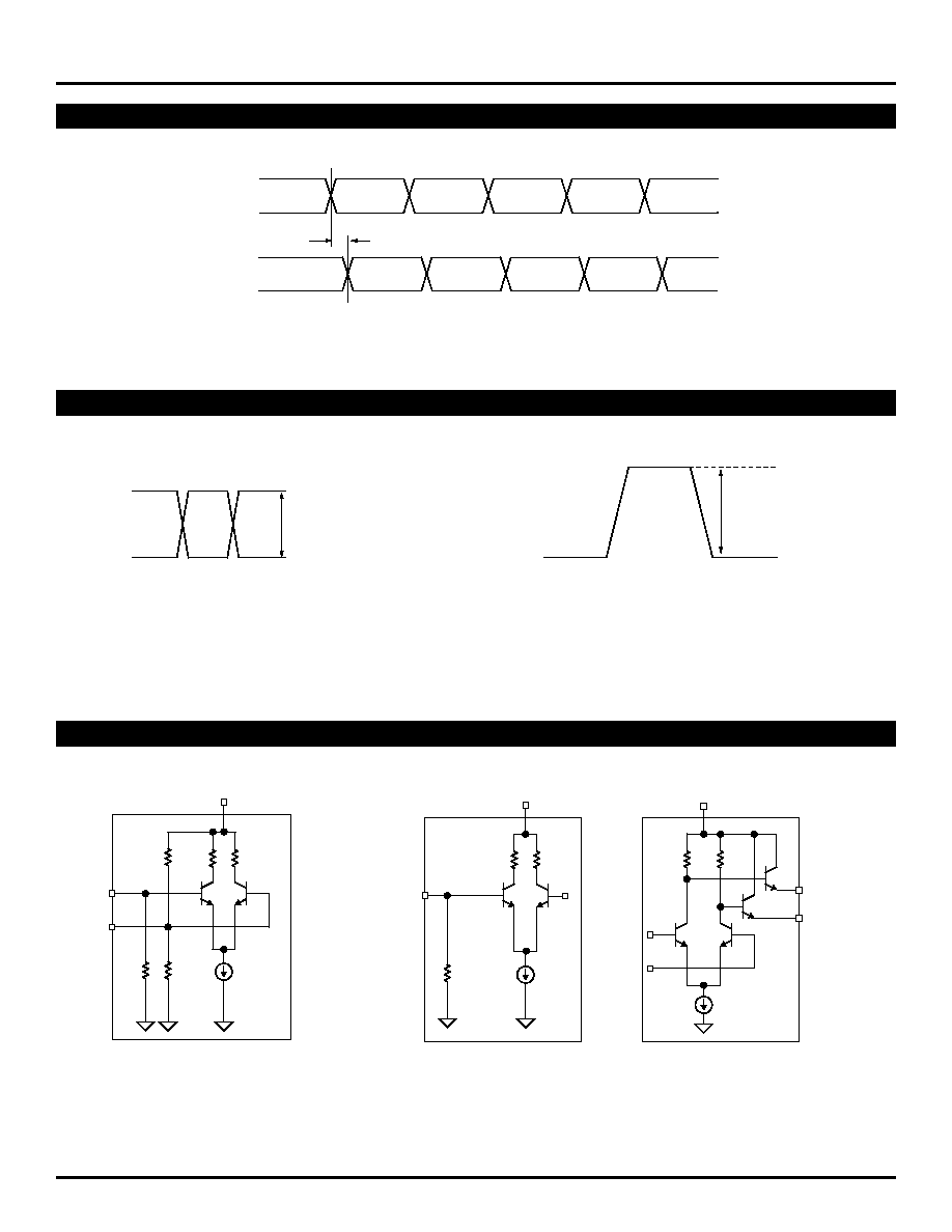
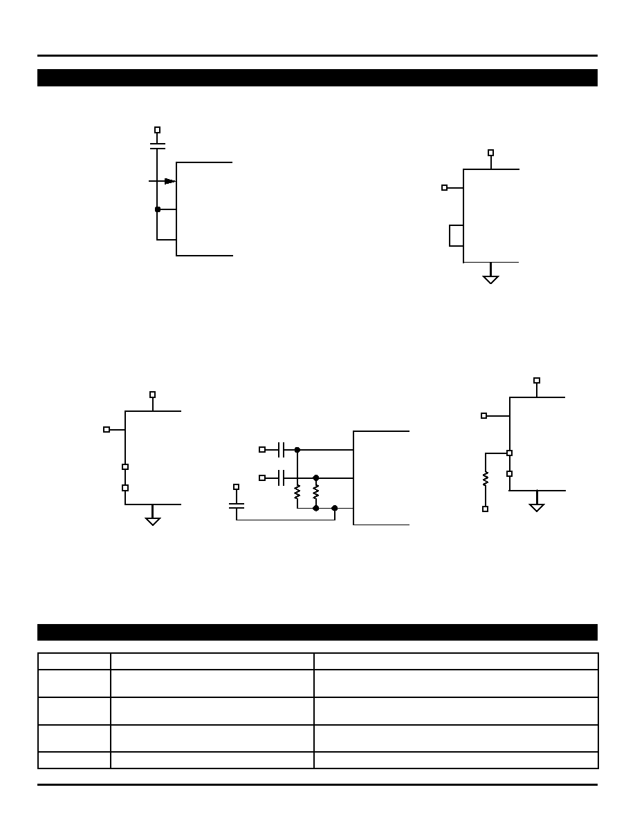
SINGLE-ENDED AND DIFFERENTIAL SWINGS
V
IN
,
V
OUT
800mV (Typ.)
Figure 1a. Single-Ended Voltage Swing
INPUT AND OUTPUT STAGES
V
DIFF_IN
,
V
DIFF_OUT
1.6V (Typ.)
Figure 1b. Differential Voltage Swing
V
CC
IN
/IN
75k9
75k9
75k9
Figure 2a. Differential
Input Stage
V
CC
/EN
LEN
SETMIN
SETMAX
D[0:10]
V
BB
75k9
Figure 2b. Single-Ended
Input Stage
V
CC
Q, CASCADE
/Q, /CASCADE
Figure 3. LVPECL
Output Stage
10
Precision EdgeTM
SY89295U
Micrel
M9999-031604
hbwhelp@micrel.com or (408) 955-1690
OUTPUT INTERFACE APPLICATIONS
R2
82
R2
82
Z
0
= 50
Z
0
= 50
+3.3V
+3.3V
V
T
= V
CC
--2V
R1
130
R1
130
+3.3V
For +2.5V systems
R1 = 250
, R2 = 62.5
Q
/Q
Figure 4. Parallel Termination
50
50
Z
0
= 50
Z
0
= 50
+3.3V
V
CC
50
C (optional)
0.01
µ
F
For +2.5V systems
R1 = 19
R1
Q
/Q
Figure 5. Y-Termination
R4
1.6k
R2
82
Z
0
= 50
+3.3V
+3.3V
R1
1k
R3
1k
+3.3V
For +2.5V systems
R1 = 250
, R2 = 62.5
, R3 = 1.25k
, R4 = 1.2k
R2
82
R1
130
+3.3V
Q
/Q
Figure 6. Terminating Unused I/O
11
Precision EdgeTM
SY89295U
Micrel
M9999-031604
hbwhelp@micrel.com or (408) 955-1690
APPLICATIONS INFORMATION
For best performance, use good high-frequency layout
techniques, filter V
CC
supplies, and keep ground connections
short. Use multiple vias where possible. Also, use controlled
impedance transmission lines to interface with the SY89295U
data inputs and outputs.
V
BB
Reference
The VBB pin is an internally generated reference and is
available for use only by the SY89295U. When unused, this
pin should be left unconnected. Two common uses for V
BB
are to handle a single-ended PECL input, and to re-bias
inputs for AC-coupling applications.
If either IN or /IN are driven by a single-ended output,
V
BB
is used to bias the unused input. Please refer to Figure
10. The PECL signal driving the SY89295U may optionally
be inverted in this case.
When the signal is AC-coupled, V
BB
is used, as shown
in Figure 13, to re-bias IN and/or /IN. This ensures that
SY89295U inputs are within acceptable common mode
range.
In all cases, V
BB
current sinking or sourcing must be
limited to 0.5mA or less.
Setting D Input Logic Thresholds
In all designs where the SY89295U GND supply is at
zero volts, the D inputs can accommodate CMOS and TTL
level signals, as well as PECL or LVPECL. Figures 11, 12
and 14 show how to connect V
CF
and V
EF
for all possible
cases.
Cascading
Two or more SY89295U may be cascaded in order to
extend the range of delays permitted. Each additional
SY89295U adds about 3.2ns to the minimum delay and
adds another 10240ps to the delay range.
Internal cascade circuitry has been included in the
SY89295U. Using this internal circuitry, the SY89295U may
be cascaded without any external gating.
Examples of cascading 2, 3, or 4 SY89295U appear in
Figures 7, 8, and 9.
IN
/IN
Q
/Q
IN
/IN
Q
/Q
D[9:0]
#1
#2
SETMIN
SETMAX
/CASCADE
CASCADE
D[10]
C[9:0]
C[10]
Control Word (11bits)
Figure 7. Cascading Two SY89295U
IN
/IN
Q
/Q
IN
/IN
Q
/Q
#1
#2
SETMIN
SETMAX
SETMIN
SETMAX
/CASCADE
CASCADE
D[10]
C[11]
IN
/IN
Q
/Q
D[9:0]
#3
/CASCADE
CASCADE
D[10]
C[9:0]
C[10]
Control Word (12bits)
Figure 8. Cascading Three SY89295U
12
Precision EdgeTM
SY89295U
Micrel
M9999-031604
hbwhelp@micrel.com or (408) 955-1690
IN
/IN
Q
/Q
IN
/IN
Q
/Q
SETMIN
SETMAX
SETMIN
SETMAX
/CASCADE
CASCADE
D[10]
C[11]
IN
/IN
Q
/Q
SETMIN
#1
#2
#3
SETMAX
IN
/IN
Q
/Q
D[9:0]
/CASCADE
CASCADE
D[10]
C[9:0]
C[10]
Control Word (12bits)
#4
Figure 9. Cascading Four SY89295U
13
Precision EdgeTM
SY89295U
Micrel
M9999-031604
hbwhelp@micrel.com or (408) 955-1690
INTERFACE APPLICATIONS
LVPECL
Input*
V
BB
V
CC
IN
0.01mF
/IN
* 3.3V single-ended only, 2.5V,
single-ended is not functional.
Figure 10. Interfacing to a
Single-Ended LVPECL Signal
To invert the signal, connect the LVPECL
input to /IN and connect V
CC
to IN.
V
EF
V
CF
D[0:10]
LVPECL
Signals
V
CC
= +3.3V
Figure 11. V
CF
/V
EF
Biasing for
LVPECL Control (D) Input
V
EF
V
CF
NC
NC
D[0:10]
CMOS
Inputs
V
CC
= +3.3V
Figure 12. V
CF
/V
EF
Biasing for
CMOS Control (D) Input
50
50
V
BB
IN
/IN
V
CC
0.01
µ
F
Figure 13. Re-Biasing an
AC-Coupled Signal
V
EF
NC
V
CF
D[0:10]
TTL
Inputs
V
CC
= +3.3V
0V
1.5k
Figure 14. V
CF
/V
EF
Biasing for
LVTTL Control (D) Input
Part Number
Function
Data Sheet Link
SY89295U
2.5/3.3V 1.5GHz Precision LVPECL
www.micrel.com/product-info/products/sy89295u.shtml
Programmable Delay
SY89296U
2.5/3.3V 1.5GHz Precision LVPECL
www.micrel.com/product-info/products/sy89296u.shtml
Programmable Delay with Fine Tune Control
16-MLF Manufacturing Guidelines
www.amkor.com/products/notes_papers/MLF_appnote_0902.pdf
Exposed Pad Application Note
HBW Solutions
http://www.micrel.com/product-info/as/solutions.shtml
RELATED PRODUCT AND SUPPORT DOCUMENTATION
14
Precision EdgeTM
SY89295U
Micrel
M9999-031604
hbwhelp@micrel.com or (408) 955-1690
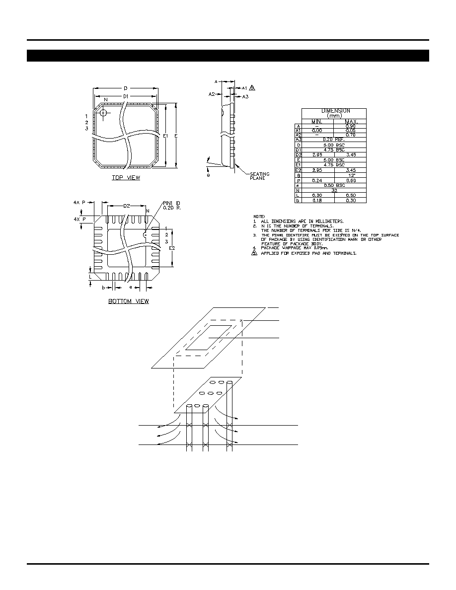
32 LEAD
MicroLeadFrameTM (MLF-32)
Package
EP- Exposed Pad
Die
CompSide Island
Heat Dissipation
Heavy Copper Plane
Heavy Copper Plane
V
EE
V
EE
Heat Dissipation
PCB Thermal Consideration for 32-Pin MLFTM Package
(Always solder, or equivalent, the exposed pad to the PCB)
Package Notes:
1. Package meets Level 2 qualification.
2. All parts are dry-packaged before shipment.
3. Exposed pads must be soldered to a ground for proper thermal management.
Rev. 01
15
Precision EdgeTM
SY89295U
Micrel
M9999-031604
hbwhelp@micrel.com or (408) 955-1690
MICREL, INC.
1849 FORTUNE DRIVE
SAN JOSE, CA 95131
USA
TEL
+ 1 (408) 944-0800
FAX
+ 1 (408) 944-0970
WEB
http://www.micrel.com
The information furnished by Micrel in this data sheet is believed to be accurate and reliable. However, no responsibility is assumed by Micrel for its use.
Micrel reserves the right to change circuitry and specifications at any time without notification to the customer.
Micrel Products are not designed or authorized for use as components in life support appliances, devices or systems where malfunction of a product can
reasonably be expected to result in personal injury. Life support devices or systems are devices or systems that (a) are intended for surgical implant into
the body or (b) support or sustain life, and whose failure to perform can be reasonably expected to result in a significant injury to the user. A Purchaser's
use or sale of Micrel Products for use in life support appliances, devices or systems is at Purchaser's own risk and Purchaser agrees to fully indemnify
Micrel for any damages resulting from such use or sale.
© 2004 Micrel, Incorporated.
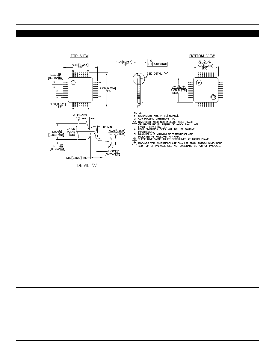
32 LEAD TQFP (T32-1)
Rev. 01