
SM625/SM626/SM627
4/90 Rev 1.1 2/94
L
INFINITY
Microelectronics Inc.
Copyright
©
1994
11861 Western Avenue
Garden Grove, CA 92841
1
(714) 898-8121
FAX: (714) 893-2570
FEATURES
∑∑
∑∑
∑
Equivalent to the Unitrode PIC 625, 626, 627
∑∑
∑∑
∑
15A current capability
∑∑
∑∑
∑
Designed and characterized for switching regulator
applications such as Buck, Boost, and Buck-Boost
type
∑∑
∑∑
∑
Cost saving design reduces size, improves efficiency,
reduces noise and RFI
∑∑
∑∑
∑
High operating frequency (to > 100KHz) results in
smaller inductor-capacitor filter and improved power
supply response time
∑∑
∑∑
∑
High operating efficiency at 7A typical performance -
Rise and fall time < 300ns
Efficiency > 85%
∑∑
∑∑
∑
Electrically isolated, 4-pin, TO-66 hermetic case
HIGH RELIABILITY FEATURES
Available with high reliability processing
DESCRIPTION
The SM625/626/627 series of Power Output Stages are espe-
cially designed to be driven with standard PWM integrated
circuits to form an efficient switching power supply. The SM625,
SM626 and SM627 are optimized for non-isolated Buck and
Buck-Boost application. The hybrid circuit construction utilizes
thick film resistors on a beryllia substrate for maximum thermal
conductivity and resultant low thermal impedance. All of the
active elements in the hybrid are fully passivated.
FUNCTIONAL DIAGRAM
SM625/SM626/SM627
SWITCHING REGULATOR POWER OUTPUT STAGES
SM625/SM626/SM627
4/90 Rev 1.1 2/94
L
INFINITY
Microelectronics Inc.
Copyright
©
1994
11861 Western Avenue
Garden Grove, CA 92841
2
(714) 898-8121
FAX: (714) 893-2570
ABSOLUTE MAXIMUM RATINGS
(Note 1)
150
∞
C
-65
∞
C to 150
∞
C
300
∞
C
Operating Junction Temperature
Hermetic (R Package) ..................................................
Storage Temperature Range .............................
Lead Temperature (Soldering, 10 Seconds) ....................
4.0
∞
C/W
4.0
∞
C/W
60.0
∞
C/W
Thermal Resistance
Power Switch,
J - C
...................................................
Commutating Diode ..................................................
Case to Ambient,
C - A
............................................
Note 1. Exceeding these ratings could cause damage to the device.
R Package:
Thermal Resistance-
Junction to Case
,
JC
.................. 4.0∞C/W
Thermal Resistance-
Junction to Ambient
,
JA
.............. 40∞C/W
THERMAL DATA
Note A. Junction Temperature Calculation: T
J
= T
A
+ (P
D
x
JA
).
Note B. The above numbers for
JC
are maximums for the limiting
thermal resistance of the package in a standard mount-
ing configuration. The
JA
numbers are meant to be
guidelines for the thermal performance of the device/pc-
board system. All of the above assume no ambient
airflow.
SM625
SM626
SM627
Input Voltage, V
4 - 2
.........................................
60V
80V
100V
Output Voltage, V
1 - 2
......................................
60V
80V
100V
Drive Input Reverse Voltage, V
3 - 4
.................
5V
5V
5V
Output Current, I
1
..........................................
15A
15A
15A
Drive Current, I
3
.............................................
-0.4A
-0.4A
-0.4A
RECOMMENDED OPERATING CONDITIONS
(Note 2)
Operating Ambient Temperature Range
SM6XXR ....................................................... 0
∞
C to 70
∞
C
SM6XXHRR ........................................... -55
∞
C to 125
∞
C
Note 2. Range over which the device is functional.
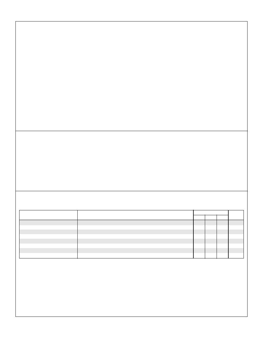
ELECTRICAL CHARACTERISTICS
(Unless otherwise specified, these specifications apply for the operating ambient temperature of T
A
= 25
∞
C. Low duty cycle pulse testing tech-
niques are used which maintains junction and case temperatures equal to the ambient temperature.)
I
4
= 7A(-7A), I
3
= -30mA (30mA)
I
4
= 15A(-15A), I
3
= -30mA (30mA)
I
4
= 7A(-7A)
I
4
= 15A(-15A)
V
4
= Rated input voltage
V
4
= Rated input voltage, T
A
= 125
∞
C
V
1
= Rated output voltage
V
1
= Rated output voltage, T
A
= 125
∞
C
On-State Voltage
(Note 3)
Diode Forward Voltage
(Note 3)
Off-State Current
Diode Reverse Current
V
V
V
V
µ
A
µ
A
µ
A
µ
A
Test Conditions
Parameter
Units
Note 3. Pulse test: Duration = 300
µ
s, Duty Cycle
2%.
SM625
SM626
SM627
Input Voltage, V
4 - 2
.........................................
50V
70V
90V
Output Voltage, V
1 - 2
......................................
50V
70V
90V
Drive Input Reverse Voltage, V
3 - 4
.................
4V
4V
4V
Output Current, I
1
..........................................
13A
13A
13A
Drive Current, I
3
............................................. -0.3A
-0.3A
-0.3A
1.5
3.5
1.25
1.75
10
10
SG625/626/627
Min.
Typ. Max.
1.0
2.5
0.85
0.95
0.1
10
1.0
500

SM625/SM626/SM627
4/90 Rev 1.1 2/94
L
INFINITY
Microelectronics Inc.
Copyright
©
1994
11861 Western Avenue
Garden Grove, CA 92841
3
(714) 898-8121
FAX: (714) 893-2570
Current Delay Time
Current Rise Time
Voltage Rise Time
Voltage Storage Time
Voltage Fall Time
Current Fall Time
Efficiency
(Note 5)
Test Conditions
Parameter
Units
ELECTRICAL SPECIFICATIONS
(continued)
Note 4. In switching an inductive load, the current will lead the voltage on turn-on and lag the voltage on turn-off (see Figure 2). Therefore, Voltage
Delay Time (t
DV
)
t
di
+ t
ri
and Current Storage Time (t
si
)
t
sv
+ t
fv
.
Note 5. The efficiency is a measure of internal power losses and is equal to Output Power divided by Input Power. The switching speed circuit of Figure
1, in which the efficiency measured, is represenative of typical operating conditions for the SM600 series switching regulators.
Dynamic Characteristics (See Figures 1 & 2)
(Notes 4 & 5)
AC TEST CIRCUIT AND SWITCHING TIME WAVEFORMS
(Note 6)
FIGURE 1 - SM625/626/627 SWITCHING SPEED CIRCUIT
FIGURE 2 - SM625/626/627 SWITCHING WAVEFORMS
SM625
SM626
SM627
ns
ns
ns
ns
ns
ns
%
60
150
60
175
300
35
65
40
700
70
175
85
SG625/626/627
Min.
Typ. Max.
FIGURE 4 - NEGATIVE OUTPUT DOWN/UP (BUCK-BOOST) CONVERTER
FIGURE 3 - STEP DOWN (BUCK) CONVERTER
APPLICATION CIRCUITS
SM62X
SM62X
