 | –≠–ª–µ–∫—Ç—Ä–æ–Ω–Ω—ã–π –∫–æ–º–ø–æ–Ω–µ–Ω—Ç: ML5824 | –°–∫–∞—á–∞—Ç—å:  PDF PDF  ZIP ZIP |

ML5824
ML5824 2.4GHz to 5.8GHz Frequency Translator
Final Datasheet
DS5824-F-01
AUGUST
2004
GENERAL DESCRIPTION
The ML5824 is a high integration 2.4GHz - 5.8GHz
frequency translator (transverter). It upconverts 2.4GHz
signals to 5.8GHz and downconverts received 5.8GHz
signals to 2.4GHz. Transmit and receive utilize the
same low noise fixed local oscillator (LO). It is intended
to be used in conjunction with a 2.4GHz transceiver-
based solution to quickly and easily develop a 5.8GHz
solution while fully leveraging previous development.
The ML5824 receive chain contains a Low Noise
Amplifier (LNA), bandpass filter and image reject down
conversion mixer. A digitally controlled 18dB gain step
in the receive chain provides an innovative solution for
optimizing IIP3 (low gain mode) and Noise Figure (high
gain mode). On the transmit side, the ML5824 buffers
and upconverts a differential 2.4GHz signal to 5.8GHz,
where it is filtered and amplified.
The ML5824's PLL accepts two industry-standard input
clock frequencies. The ML5824's low STANDBY MODE
current maximizes battery life. Power supply regulation
is included in the ML5824, providing circuit isolation
and consistent performance over supply voltages
between 2.8V-3.6V.
PIN CONFIGURATION
TXISET
TXIN
TXIP
VREG3
VBG2
VREG2
VTUNE
VSSLO
VMIX
VSSMX
RXON
RXOP
RFISET
RXGN
VCCA
FREF
RE
FSE
L
TXO
N
XC
EN
VRE
G
1
QP
O
VS
SPL
L
V
LNA
RX
I
V
RE
G4
V
BG
1
V
TXB
TXO
* GROUND/RETURN ON EXPOSED PADDLE
PIN 1
*
ORDERING INFORMATION
PART NUMBER TEMP RANGE
PACKAGE
PACK (QTY)
ML5824EM -10
o
C to +70
o
C 28LPCC 4x5x0.9 mm Antistatic Tray (490)
ML5824EM-T -10
o
C to +70
o
C 28LPCC 4x5x0.9 mm Tape & Reel (2500)
FEATURES
High Integration 2.4GHz to 5.8GHz Transverter
Receive LNA, Image Reject Filter & Mixer
Transmit Pre-Driver, Filters & Mixers
Fully Integrated PLL-Based Synthesizer
Selectable Receive Gain Optimizes NF and IIP3
Interfaces
Directly
with
Many 2.4GHz Transceivers
4dB (typ. High Gain Mode) Noise Figure
-14dBm Input IP3 (Low Gain Mode)
Selectable Transmit Output Power
10
µ
A Standby Mode
Space-saving 28 pin LPCC package
APPLICATIONS
5.8GHz Digital Cordless Telephones
5.8GHz Streaming Audio & Video
Upconverted
2.4GHz
Standards
o
Bluetooth
o
Zigbee/802.15.4
BLOCK DIAGRAM
FREF
TXO
TX Subsystem
RXI
RX Subsystem
RXON, RXOP
TXIN, TXIP
REFSEL
TXON
XCEN
Control
Logic
QPO VTUNE
2380-2505 MHz
5725-5850 MHz
2380-2505 MHz
5725-5850 MHz
GAIN
CONTROL
RXGN
TXISET
2
2
PLL
Supply
Regulation
& Voltage
Reference
VCCA
VBG1
VBG2
VREGn
RFISET
Top View

DS5824-F-01
FINAL DATASHEET
AUGUST 2004
2
TABLE OF CONTENTS
GENERAL DESCRIPTION ........................................................................................................................................... 1
PIN CONFIGURATION ................................................................................................................................................. 1
ORDERING INFORMATION ........................................................................................................................................ 1
FEATURES ................................................................................................................................................................... 1
APPLICATIONS ............................................................................................................................................................ 1
BLOCK DIAGRAM........................................................................................................................................................ 1
TABLE OF CONTENTS................................................................................................................................................ 2
SIMPLIFIED APPLICATIONS DIAGRAM ..................................................................................................................... 2
ELECTRICAL CHARACTERISTICS............................................................................................................................. 3
PIN DESCRIPTIONS.................................................................................................................................................... 5
FUNCTIONAL DESCRIPTION ..................................................................................................................................... 9
MODES OF OPERATION............................................................................................................................................. 9
PHYSICAL DIMENSIONS .......................................................................................................................................... 11
WARRANTY................................................................................................................................................................ 12
SIMPLIFIED APPLICATIONS DIAGRAM
Figure 1: ML5824 Typical Application Schematic
DS5824-F-01
FINAL DATASHEET
AUGUST 2004
3
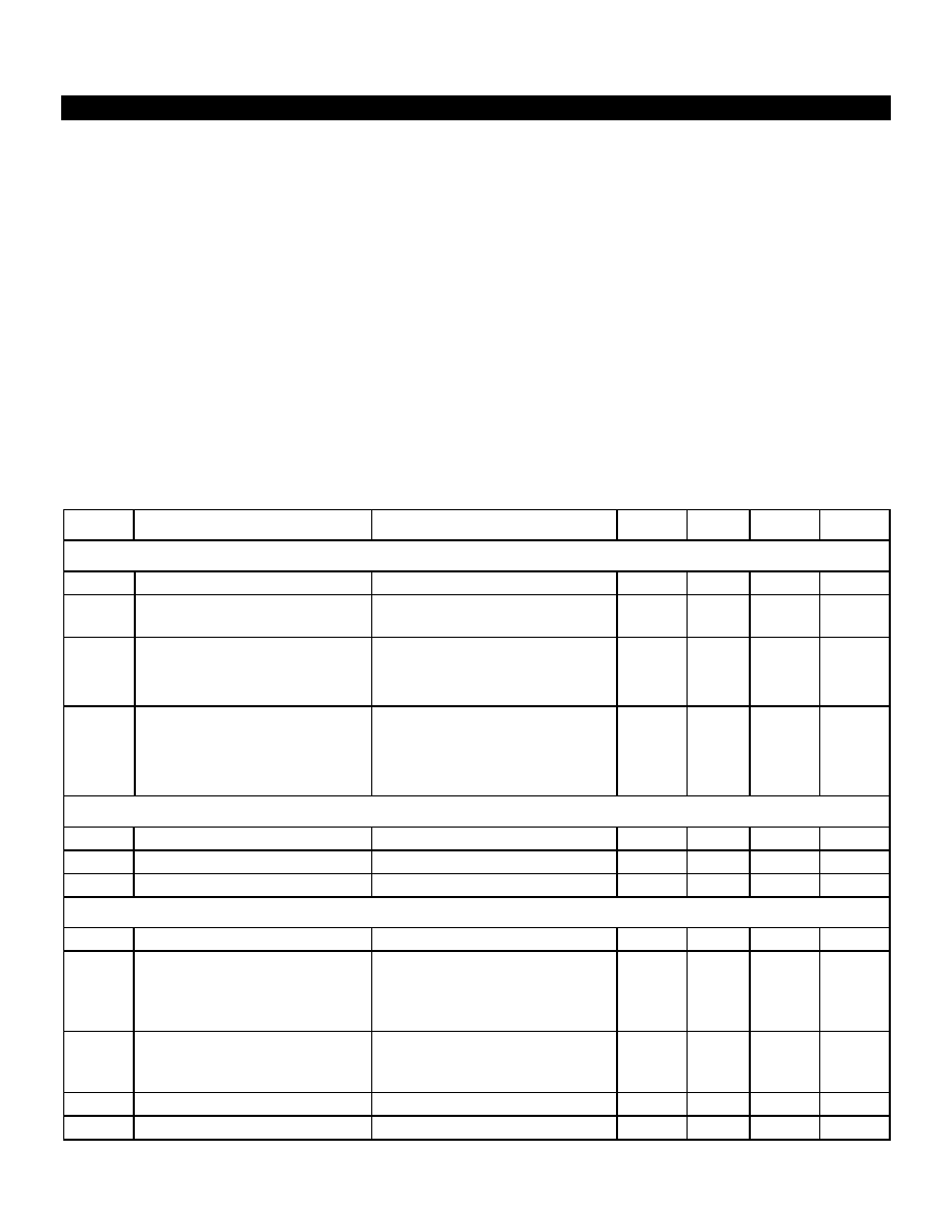
ELECTRICAL CHARACTERISTICS
ABSOLUTE MAXIMUM RATINGS
Absolute maximum ratings are those values beyond which the device could be permanently damaged. Absolute
maximum ratings are stress ratings only and functional device operation is not implied. Operating the device for any
length of time beyond the operating conditions may degrade device performance and/or shorten operating lifetime.
VCCA.......................................................................................................................................................................... 3.6 V
Maximum Receive RF Input Power.......................................................................................................................+13dBm
Maximum Transmit RF Input Power........................................................................................................................+3dBm
Junction Temperature............................................................................................................................................... 150∞C
Storage Temperature Range ...................................................................................................................... -65∞C to 150∞C
Lead Temperature (Soldering, 10s).......................................................................................................................... 260∞C
Thermal Resistance (
JA
) ........................................................................................................................................ 39∞C/W
OPERATING CONDITIONS
Ambient Temperature Range ....................................................................................................................... -10∞C to 70∞C
VCCA Range ...................................................................................................................................................2.8V to 3.6V
Unless otherwise specified, V
CCA
=3.2V, T
A
=-10∞C to +70∞C, XCEN=V
IH
, P
INRX
=-40dBm, P
INTX
=-3dBm, PLL Loop Filter
Bandwidth=40 KHz, and gain control in either state.
SYMBOL PARAMETER
CONDITIONS
MIN
TYP
MAX
UNITS
POWER SUPPLIES
VCCA
Analog supply voltage
2.8
3.2
3.6
V
I
STBY
Supply current, STANDBY mode
VCCA=3.6V, XCEN=V
IL
,
TXON= V
IL
OR V
IH
10
µ
A
I
RX
Supply current, RECEIVE mode
at -10dBm max RF input
TXON= V
IL
TXON= V
IL,
TA=50∞C
TXON= V
IL,
TA=25∞C
60
55
50
mA
mA
mA
I
TX
Supply current, TRANSMIT mode
TXON= V
IH
R
TXISET
=7.5K
R
TXISET
=5.5K
TXON= V
IH
R
TXISET
=7.5K
,
TA=50∞C
R
TXISET
=5.5K
,
TA=50∞C
95
100
95
100
110
115
105
110
mA
mA
mA
mA
SUPPLY REGULATION
V
R27
Regulated Output Voltage
Pins 12, 19, 26
2.7
V
V
R25
Regulated Output Voltage
Pin 17
2.5
V
V
BG
Bandgap Voltage
Pins 18 & 25
1.25
V
SYNTHESIZER
f
LO
Local
Oscillator
Frequency
F
OUT
= F
IN
+/- F
LO
3343.68 MHz
I
P
Charge Pump sink/source current
This is a function of V
TUNE
to
compensate for the change in K
V
V
TUNE
=0.3V
V
TUNE
=1.2V
V
TUNE
=1.9V
0.49
0.90
0.60
0.38
0.71
mA
mA
mA
N
Phase noise at driver output
f
o
=10KHz offset from f
c
f
o
=1.2MHz offset from f
c
400mVp-p sine wave reference
-65
-115
-110
dBc/Hz
dBc/Hz
K
V
VCO Tuning sensitivity
100
230
350
MHz/V
F
PULL
Frequency pulling
70
µ
s after P
IN
≠50dBm to +12dBm
+/-20 KHz
DS5824-F-01
FINAL DATASHEET
AUGUST 2004
4
SYMBOL PARAMETER
CONDITIONS
MIN
TYP
MAX
UNITS
F
PTR
Frequency pulling TX to RX
and RX to TX
70
µ
s after transition
+/-20 KHz
F
PUSH
Frequency pushing
Vary VCCA from 2.9V to 3.6V
<.5
MHz/V
t
WAKE
Lock up time from standby
XCEN=V
IH
, to within 10KHz,
200
µ
s
f
FREF
Reference signal frequency
REFSEL=V
IL
REFSEL=V
IH
10.368
13.824
MHz
MHz
V
FREF
Reference signal level
AC coupled
400
1200
mVp-p
RECEIVER
F
RXI
Receiver Input Frequency Range
5.725-5.850
GHz
F
RXO
Receiver Output Frequency Range
2.380-2.505
GHz
Z
RIN
Receiver Input Impedance
Over F
RXI
37 + j2
Z
RXO
Receiver Output Impedance
Differential Impedance RXON/RXOP
Over F
RXO
100
NF
Input noise figure
High Gain Mode
Low Gain Mode
4.0
14
7.0
22
dB
dB
G
RX
RX Power Gain High Gain Mode
High Gain Mode
High Gain Mode
Low Gain Mode
Pin=-50dBm, TA=25∞C
Pin=-50dBm, TA=50∞C
Pin=-50dBm
Pin=-30dBm
10.5
9.5
8
13
-8
dB
dB
I
IP3
Input IP3 High Gain Mode
Low Gain Mode
For Pin=-50dBm each tone spaced
+/-1MHz from 5800MHz
For Pin=-30dBm each tone spaced
+/1MHz from 5800MHz
-25
-14
dBm
dBm
P
1dB
RX Input 1dB compression
High Gain Mode
Low Gain Mode
-35
-25
dBm
dBm
P
RXI
RX conducted emissions from RF input
port
RXI terminated in 50 ohm
-50
dBm
P
SPUR
Out of Band Spurious,
High Gain Mode
Low Gain Mode
Spurs outside Receive Output Frequency
Range
-25
-5
dBc
dBc
IRR
RX Image Rejection
From RXI to RXO, Pin=-50dBm,
F
RXI
= 835-965MHz
20 dB
TRANSMITTER
F
TXI
Transmitter Input Frequency Range
2.380-2.505
GHz
F
TXO
Transmitter Output Frequency Range
5.725-5.850
GHz
Z
TXI
Transmitter Input Impedance
Differential Impedance TXIN/TXIP Over
F
TXI
100
Z
TXO
Transmitter Output Impedance
Over F
TXO
43 + j88
P
OUT
TX buffer output power at 5.85 GHz
Matched into 50 ohms, -10∞C<T
A
<70∞C
R
TXISET
=7.5K
,
Pin=-6dBm
R
TXISET
=5.5K
,
Pin=-3dBm
3.5
5.5
dBm
dBm
P
50C
TX buffer output power at 5.85 GHz
Matched into 50 ohms, -10∞C<T
A
<50∞C
R
TXISET
=7.5K
,
Pin=-6dBm
R
TXISET
=5.5K
,
Pin=-3dBm
5
7
dBm
dBm
R
TXH
Transmit harmonic output rejection
See Note 1
50 Ohm load
<-20
dBc
R
LO
Transmit LO feed thru
Measured at TXO port with CW signal at
F
TXI
and P
TXI
-30 dBc
DS5824-F-01
FINAL DATASHEET
AUGUST 2004
5
SYMBOL PARAMETER
CONDITIONS
MIN
TYP
MAX
UNITS
R
RFIF
Transmit IF feed thru
Measured at TXO port with CW signal at
F
TXI
and P
TXI
-30 dBc
R
2LO
Transmit 2xLO feed thru
See Note 1
Measured at TXO port with CW signal at
F
TXI
and P
TXI
<-30 dBc
R
3LO
Transmit 3xLO feed thru
See Note 1
Measured at TXO port with CW signal at
F
TXI
and P
TXI
<-20 dBc
R
4LO
Transmit 4xLO feed thru
See Note 1
Measured at TXO port with CW signal at
F
TXI
and P
TXI
<-20 dBc
R
TSB
Transmit lower sideband rejection
From TXI to TXO ports at P
TXI
for
F
TXO
= 835-960MHz
25 dBc
R
MXN
Mixer products rejection at output port
See Note 1
From TXI to TXO ports at P
TXI
for
F
TXO
= 960-970MHz
>55 dBc
INTERFACE LOGIC LEVELS
Input pins (XCEN, TXON, RXGN, REFSEL)
V
IH
Input high voltage
VCCA*0.7 VCCA+0.4
V
V
IL
Input low voltage
-0.4
VCCA*0.3
V
I
B
Input bias current
All states
-5
5
µ
A
C
IN
Input capacitance
1MHz test frequency
4
pF
Note 1: Typical specs represent a 3 sigma data point at sample test.
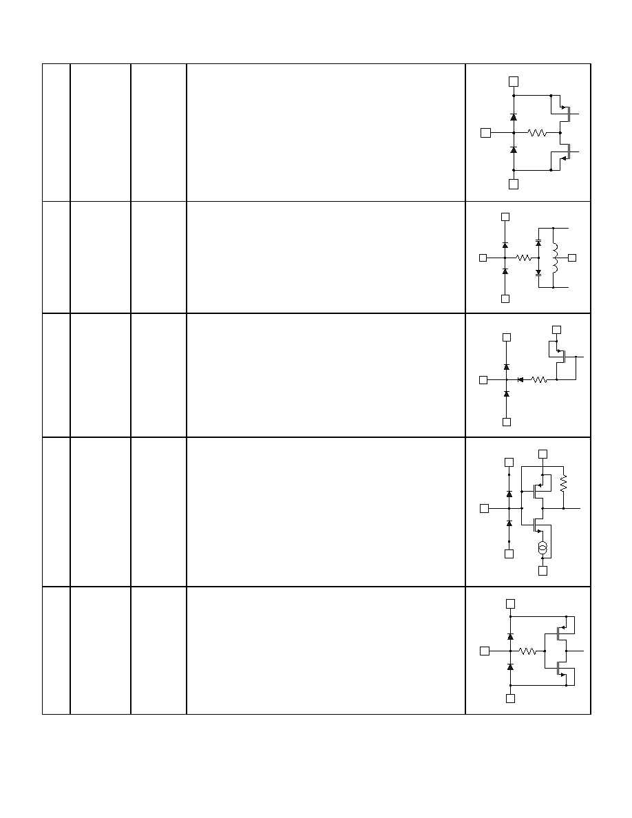
PIN DESCRIPTIONS
PIN NAME
I/O
FUNCTION
DIAGRAM
POWER & GROUND
2 VSSMX
GROUND Mixer
Ground
N/A
7
VCCA
POWER
Regulated External Supply, Requires Proper Decoupling Components
N/A
14 VSSPLL
GROUND PLL
Ground
N/A
15
VSSLO
GROUND
VCO and LO Ground
N/A
24
VTXB
INPUT
TX Buffer Supply Voltage, Connect to Pin 7
N/A
X
VSSDB
GROUND
Exposed Paddle. Ground/Return
N/A
SUPPLY REGULATION
1
VMIX
INPUT
2.7V Supply Decoupling Point, Connect to Pin 26
N/A
12
VREG1
OUTPUT
2.7V Regulated Supply Output
N/A
17
VREG2
OUTPUT
2.5V Regulated Supply Output
N/A
18
VBG2
OUTPUT
1.24V Bandgap2 Supply Decoupling Point
N/A
19
VREG3
OUTPUT
2.7V Regulated Supply Decoupling Point
N/A
25
VBG1
OUTPUT
1.24V Bandgap1 Supply Decoupling Point
N/A
26
VREG4
OUTPUT
2.7V Regulated Supply Output, Connect to Pins 1 and 28
N/A
28
VLNA
INPUT
2.7V LNA Supply Decoupling Point, Connect to Pin 26
N/A
DS5824-F-01
FINAL DATASHEET
AUGUST 2004
6
RF TRANSMIT/RECEIVE DATA
27
RXI
I (analog)
5.8GHz RX Input. A simple matching network is required for optimum
noise figure. This input connects to the base of an NPN transistor and
should be AC coupled.
28
VSSDB
VLNA
27
RXI
3.9K
0.7V
23
TXO
O (analog)
5.8GHz TX Output into a matched load over the 5725 to 5850 MHz
range.
24
VSSDB
VTXB
23
TXO
4
3
RXOP
RXON
O (analog)
Differential 2.4GHz RX Output.
7
2
VSSMX
VCCA
4
RXOP
56
VSSDB
20
21
TXIP
TXIN
I (analog)
Differential 2.4GHz TX Input
7
2
VSSMX
VCCA
22
82
X
VSSDB
20
TXIP
21
TXIN

DS5824-F-01
FINAL DATASHEET
AUGUST 2004
7
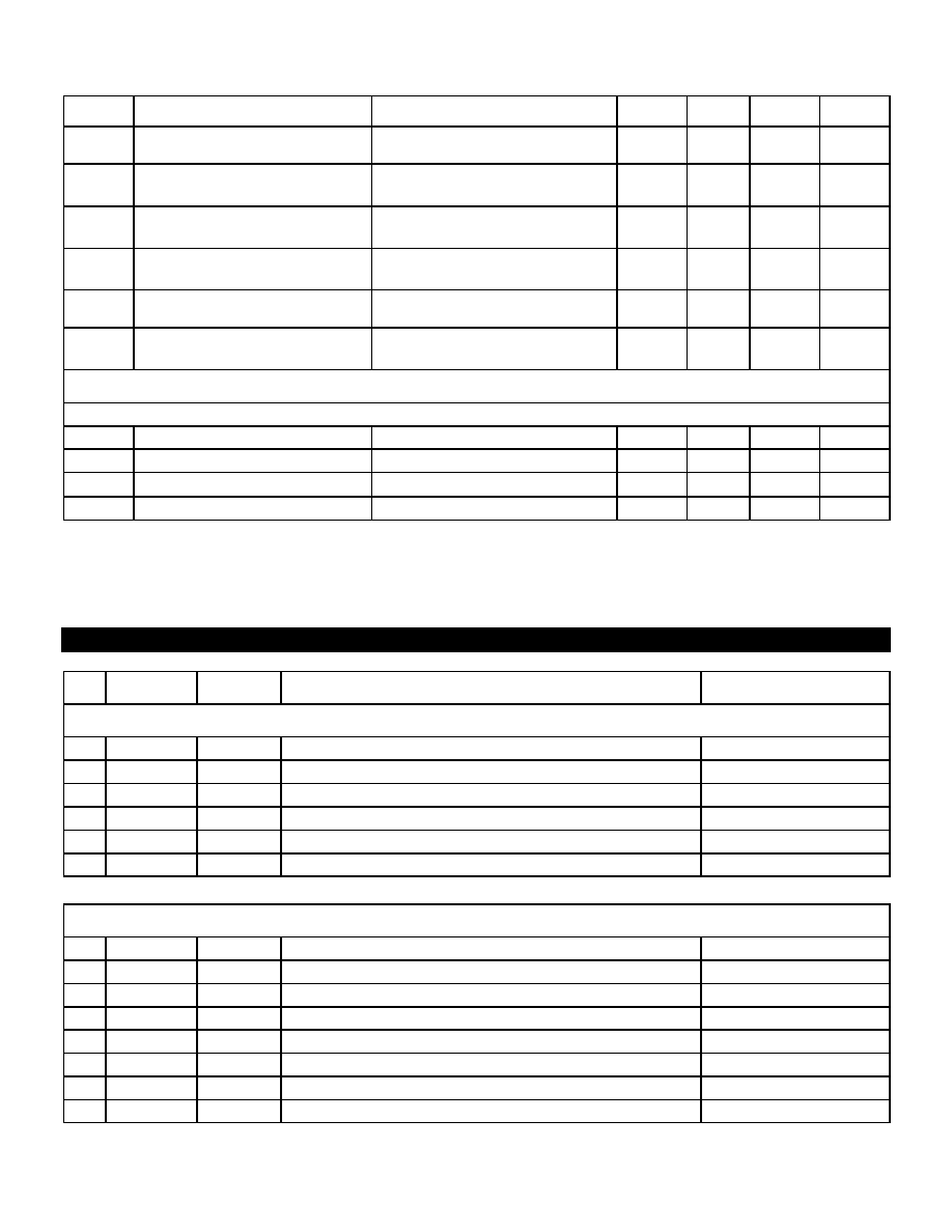
RF CONTROL & OTHERS
11
XCEN
I (CMOS)
Transceiver Enable Input. Enables the bandgap reference and voltage
regulators when high. Consumes only leakage current in STANDBY
mode when low. This is a CMOS input, and the thresholds are
referenced to VCCA and VSSMX.
7
2
VSSMX
VCCA
11
168
XCEN
10
TXON
I (CMOS)
TX/RX Control Input. Switches the transceiver between TRANSMIT and
RECEIVE modes. Circuits are powered up and signal paths reconfigured
according to the operating mode. This is a CMOS input, and the
thresholds are referenced to VCCA and VSSMX.
7
2
VSSMX
VCCA
10
168
TXON
5 RFISET
I
(analog) Connect to a 255
+/-1% resistor to ground.
7
2
VSSMX
VCCA
5
RFISET
6
RXGN
I (CMOS)
Gain Step Input Control. Switches the receiver between high gain (when
HIGH) and low gain (when LOW). This dual-gain design allows the
system designer to achieve low noise figure for low input signals while
maintaining a good IIP3 under high input signal conditions. This is a
CMOS input, and the thresholds are referenced to VCCA and VSSMX.
7
2
VSSMX
VCCA
6
168
RXGN
DS5824-F-01
FINAL DATASHEET
AUGUST 2004
8
13
QPO
O (analog)
Charge Pump Output. This output is connected to the external PLL loop
filter. Sources current when the LO frequency is lower than desired.
12
14
VSSPLL
VREG1
13
QPO
9.2
16
VTUNE
I (analog)
VCO Tuning Voltage. This input from the PLL loop filter determines the
output frequency and is very sensitive to noise coupling and leakage
currents.
19
15
VSSLO
VREG3
16
VTUNE
17
VREG2
10
22
TXISET
I (analog)
A resistor between this pin and ground establishes the PA output power
compression point by setting a bias current.
7
2
VSSMX
VCCA
22
TXISET
24
VTXB
522
8
FREF
I (analog)
Input Reference Frequency. Depending on the state of the REFSEL pin
this input is divided by 3 or 4 to generate the PLL reference frequency.
7
2
VSSMX
VCCA
8
FREF
12
14
VSSPLL
VREG1
9
REFSEL
I (CMOS)
Reference Divider Control. If REFSEL is HIGH, FREF is divided by 4,
otherwise FREF is divided by 3. This is a CMOS input, and the
thresholds are referenced to VCCA and VSSMX.
7
2
VSSMX
VCCA
9
168
REFSEL
DS5824-F-01
FINAL DATASHEET
AUGUST 2004
9
FUNCTIONAL DESCRIPTION
The ML5824 is a monolithic, bilateral 2.4GHz to 5.8GHz frequency translator. It provides a simple and straightforward
solution for designers of 2.4GHz products who want to develop advanced products for the relatively interference-free
5.8GHz band, especially digital cordless telephones. The ML5824 can implement "dual band" solutions that use both
the 2.4GHz and 5.8GHz bands as well as "hybrid" products where one link (say, basestation transmission) is at 5.8GHz,
while the other link (basestation receive) is at 2.4GHz.
5.8GHz signals enter the RXI pin and then are fed to an LNA and bandpass filter. An image-reject downconvert mixer
translates the signal to the 2.4GHz ISM band where it is then buffered and sent off chip differentially on RXON/RXOP.
The receive signal path can be configured for either a "High Gain" mode (about 14dB) or "Low Gain" mode (-4dB). Gain
mode is selected via the RXGN digital input pin. High Gain mode is used for low-level input signals to minimize Noise
Figure while Low Gain mode optimizes input IP3 for stronger signals.
2.4GHz signals come into the ML5824 differentially on the TXIP/TXIN pins, where they are upconverted to 5.8GHz,
bandpass filtered, and then amplified and exit via TXO. The predriver/buffer output power compression point is
programmed by an external resistor that sets the preamp bias level.
A fully integrated phase locked loop (PLL) generates the fixed local oscillator (LO) at 3343.68MHz which is used for
upconverting and downconverting the RF signals. The comparison frequency of the PLL is derived from the frequency
reference present on the FREF pin and the state of REFSEL as shown in Table 1. The PLL loop filter is external to the
ML5824 so that lock time and in-band phase noise can be optimized for the system of interest.
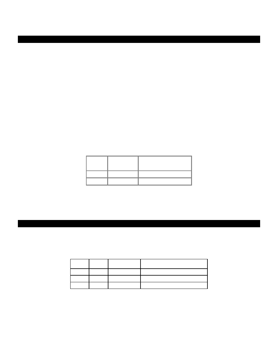
REFSEL REFERENCE
DIVISION
FREF
V
IL
3
10.368MHz
V
IH
4
13.824MHz
Table 1: ML5824 Frequency References
The ML5824 contains two separate bandgap references and several low dropout (LDO) voltage regulators to insure
consistent performance over supply voltage and minimize crosstalk on chip. The device is enabled by bringing XCEN to
V
IH
and is placed in transmit mode by setting TXON to V
IH
. With XCEN at V
IL
the ML5824 enters a low power standby
mode.
MODES OF OPERATION
The ML5824 has three key modes of operation. The two operational modes are RECEIVE and TRANSMIT, controlled
by TXON. XCEN is the chip enable/disable control pin, which sets the device in operational or STANDBY modes. The
relationship between the parallel control lines and the mode of operation of the IC is summarized in Table 2.
XCEN TXON MODE
NAME
FUNCTION
0
X
STANDBY
Standby. All circuits powered down
1
0
RECEIVE
Receive Chain Active
1 1 TRANSMIT
Transmit
Chain
Active
Table 2: Modes of Operation
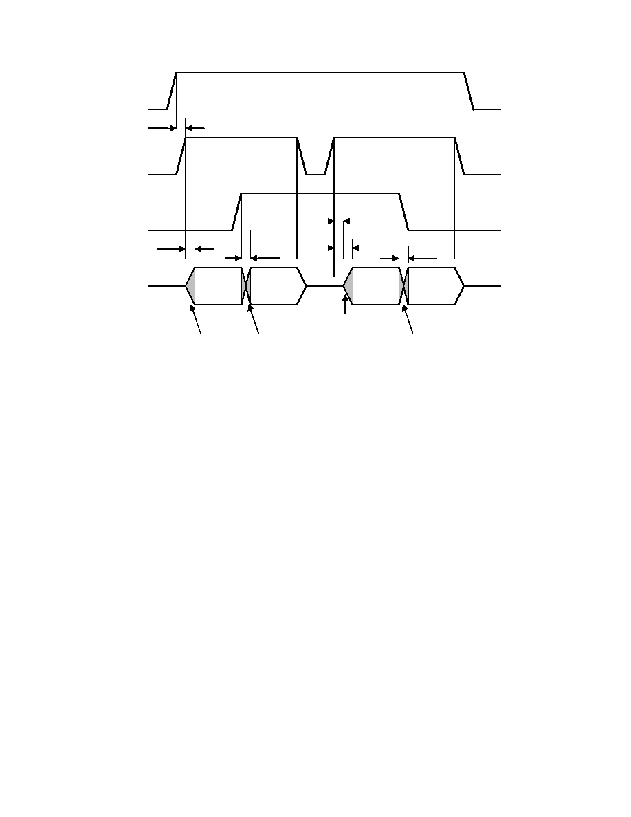
STANDBY MODE
In STANDBY mode, the ML5824 transverter is powered down. When exiting STANDBY mode, the transmitter is
disabled for 200
µ
s. However, the receive path is not similarly locked out and so will receive invalid data for up to 200
µ
s.
Therefore, the system should wait 200
µ
s after exiting STANDBY mode before actively processing signals to allow the
PLL to lock. A timing diagram for the ML5824 is shown in Figure 2.
DS5824-F-01
FINAL DATASHEET
AUGUST 2004
10
Figure 2: ML5824 Control Timing Diagram, assuming a 40 KHz loop bandwidth.
RECEIVE MODE
In RECEIVE mode, the received signal at 5.8GHz is amplified, filtered, and downconverted to 2.4GHz. The receiver has
two gain modes; High Gain (about 14dB) and Low Gain (about -4dB). Gain mode is set via the state of the RXGN input,
with High Gain Mode corresponding to a logic "1" on RXGN.
TRANSMIT MODE
In TRANSMIT mode, the transmitted signal at 2.4GHz is upconverted, filtered, and amplified at 5.8GHz. The transmit
output power compression point is programmable via an external resistor on the TXISET pin.
VCCA
XCEN
TXON
Data
Output
(RX & TX)
RX Valid
Data
Output
TX Valid
Data
Output
TX Valid
Data
Output
RX Valid
Data
Output
200uS
100uS
170uS
350uS
100uS
200uS
Supply and
PLL Settling
200uS
PLL Settling
100uS
Supply Settling
And TX Timer
170uS
Time to valid TX
data is 400uS
PLL Settling
100uS

DS5824-F-01
FINAL DATASHEET
AUGUST 2004
11
PHYSICAL DIMENSIONS
Figure 3: 28 Leadless Plastic Chip Carrier (LPCC) Dimensions

DS5824-F-01
FINAL DATASHEET
AUGUST 2004
12
WARRANTY
Micro Linear makes no representations or warranties with respect to the accuracy, utility, or completeness of the
contents of this publication and reserves the right to make changes to specifications and product descriptions at any
time without notice. No license, express or implied, by estoppel or otherwise, to any patents or other intellectual
property rights is granted by this document. The circuits contained in this document are offered as possible applications
only. Particular uses or applications may invalidate some of the specifications and/or product descriptions contained
herein. The customer is urged to perform its own engineering review before deciding on a particular application. Micro
Linear assumes no liability whatsoever, and disclaims any express or implied warranty, relating to sale and/or use of
Micro Linear products including liability or warranties relating to merchantability, fitness for a particular purpose, or
infringement of any intellectual property right. Micro Linear products are not designed for use in medical, life saving, or
life sustaining applications.
If this document is "Advance", its contents describe a Micro Linear
product that is currently under development. All
detailed specifications including pinouts and electrical specifications may be changed without notice. If this document is
"Preliminary", its contents are based on early silicon measurements. Typical data is representative of the product but is
subject to change without notice. Pinout and mechanical dimensions are final. Preliminary documents supersede all
Advance documents and all previous Preliminary versions. If this document is "Final", its contents are based on a
characterized product, and it is believed to be accurate at the time of publication. Final Data Sheets supersede all
previously published versions. This document is Preliminary.
© 2004 Micro Linear Corporation. All rights reserved. All other trademarks are the property of their respective owners.
Products described herein may be covered by one or more of the following U.S. patents: 4,897,611; 4,964,026;
5,027,116; 5,281,862; 5,283,483; 5,418,502; 5,508,570; 5,510,727; 5,523,940; 5,546,017; 5,559,470; 5,565,761;
5,592,128; 5,594,376; 5,652,479; 5,661,427; 5,663,874; 5,672,959; 5,689,167; 5,714,897; 5,717,798; 5,742,151;
5,747,977; 5,754,012; 5,757,174; 5,767,653; 5,777,514; 5,793,168; 5,798,635; 5,804,950; 5,808,455; 5,811,999;
5,818,207; 5,818,669; 5,825,165; 5,825,223; 5,838,723; 5.844,378; 5,844,941. Japan: 2,598,946; 2,619,299;
2,704,176; 2,821,714. Other patents are pending.
Micro Linear Corporation
2050 Concourse Drive
San Jose, CA 95131
Tel: (408) 433-5200
Fax: (408) 432-1627
www.microlinear.com