 | –≠–ª–µ–∫—Ç—Ä–æ–Ω–Ω—ã–π –∫–æ–º–ø–æ–Ω–µ–Ω—Ç: 24FC128 | –°–∫–∞—á–∞—Ç—å:  PDF PDF  ZIP ZIP |

2004 Microchip Technology Inc.
DS21191M-page 1
24AA128/24LC128/24FC128
Device Selection Table
Features
∑ Low-power CMOS technology:
- Maximum write current 3 mA at 5.5V
- Maximum read current 400
µ
A at 5.5V
- Standby current 100 nA typical at 5.5V
∑ 2-wire serial interface bus, I
2
CTM compatible
∑ Cascadable for up to eight devices
∑ Self-timed erase/write cycle
∑ 64-byte Page Write mode available
∑ 5 ms max write cycle time
∑ Hardware write-protect for entire array
∑ Output slope control to eliminate ground bounce
∑ Schmitt Trigger inputs for noise suppression
∑ 1,000,000 erase/write cycles
∑ Electrostatic discharge protection > 4000V
∑ Data retention > 200 years
∑ 8-pin PDIP, SOIC, TSSOP, MSOP and DFN
packages, 14-lead TSSOP package
∑ Standard and Pb-free finishes available
∑ Temperature ranges:
Description
The Microchip Technology Inc. 24AA128/24LC128/
24FC128 (24XX128*) is a 16K x 8 (128 Kbit) Serial
Electrically Erasable PROM (EEPROM), capable of
operation across a broad voltage range (1.8V to 5.5V).
It has been developed for advanced, low-power
applications such as personal communications or data
acquisition. This device also has a page write capabil-
ity of up to 64 bytes of data. This device is capable of
both random and sequential reads up to the 128K
boundary. Functional address lines allow up to eight
devices on the same bus, for up to 1 Mbit address
space. This device is available in the standard 8-pin
plastic DIP, SOIC (150 and 208 mil), TSSOP, MSOP,
DFN and 14-lead TSSOP packages.
Block Diagram
Package Types
*24XX128 is used in this document as a generic part number for the 24AA128/24LC128/24FC128 devices.
Part
Number
V
CC
Range
Max. Clock
Frequency
Temp.
Ranges
24AA128
1.8-5.5V
400 kHz
(1)
I
24LC128
2.5-5.5V
400 kHz
I, E
24FC128
1.8-5.5V
1 MHz
(2)
I
Note 1:
100 kHz for V
CC
< 2.5V.
2:
400 kHz for V
CC
< 2.5V.
- Industrial (I):
-40
∞
C to +85
∞
C
- Automotive (E):
-40
∞
C to +125
∞
C
HV Generator
EEPROM
Array
Page Latches
YDEC
XDEC
Sense Amp.
R/W Control
M
emory
C
ontrol
L
ogic
I/O
C
ontrol
L
ogic
I/O
A0 A1 A2
SDA
SCL
V
CC
V
SS
WP
A0
A1
A2
V
SS
V
CC
WP
SCL
SDA
1
2
3
4
8
7
6
5
24
X
X
128
PDIP/SOIC
TSSOP/MSOP *
A0
A1
A2
V
SS
1
2
3
4
8
7
6
5
V
CC
WP
SCL
SDA
TSSOP
2
4
XX1
2
8
DFN
A0
A1
A2
V
SS
WP
SCL
SDA
2
4
XX1
2
8
5
6
7
8
4
3
2
1
V
CC
NC
A0
A1
NC
A2
V
SS
NC
NC
V
CC
WP
NC
SCL
SDA
NC
2
4
XX1
2
8
1
2
3
4
14
13
12
11
5
10
6
9
7
8
Note: * Pins A0 and A1 are no-connects for the MSOP package only.
128K I
2
C
TM
CMOS Serial EEPROM

24AA128/24LC128/24FC128
DS21191M-page 2
2004 Microchip Technology Inc.
1.0
ELECTRICAL CHARACTERISTICS
Absolute Maximum Ratings
()
V
CC
.............................................................................................................................................................................6.5V
All inputs and outputs w.r.t. V
SS
......................................................................................................... -0.6V to V
CC
+1.0V
Storage temperature ...............................................................................................................................-65∞C to +150∞C
Ambient temperature with power applied ................................................................................................-40∞C to +125∞C
ESD protection on all pins
......................................................................................................................................................
4 kV
TABLE 1-1:
DC CHARACTERISTICS
NOTICE: Stresses above those listed under "Absolute Maximum Ratings" may cause permanent damage to the
device. This is a stress rating only and functional operation of the device at those or any other conditions above those
indicated in the operational listings of this specification is not implied. Exposure to maximum rating conditions for
extended periods may affect device reliability.
DC CHARACTERISTICS
Electrical Characteristics:
Industrial (I):
V
CC
= +1.8V to 5.5V
T
A
= -40∞C to +85∞C
Automotive (E):
V
CC
= +2.5V to 5.5V
T
A
= -40∞C to 125∞C
Param.
No.
Sym.
Characteristic
Min.
Max.
Units
Conditions
D1
--
A0, A1, A2, SCL, SDA, and
WP pins:
--
--
--
--
D2
V
IH
High-level input voltage
0.7 V
CC
--
V
--
D3
V
IL
Low-level input voltage
--
0.3 V
CC
0.2 V
CC
V
V
V
CC
2.5V
V
CC
< 2.5V
D4
V
HYS
Hysteresis of Schmitt Trigger
inputs (SDA, SCL pins)
0.05 V
CC
--
V
V
CC
2.5V (Note 1)
D5
V
OL
Low-level output voltage
--
0.40
V
I
OL
= 3.0 mA @ V
CC
= 4.5V
I
OL
= 2.1 mA @ V
CC
= 2.5V
D6
I
LI
Input leakage current
--
±1
µ
A
V
IN
= V
SS
or V
CC
, WP = V
SS
V
IN
= V
SS
or V
CC
, WP = V
CC
D7
I
LO
Output leakage current
--
±1
µ
A
V
OUT
= V
SS
or V
CC
D8
C
IN
,
C
OUT
Pin capacitance
(all inputs/outputs)
--
10
pF
V
CC
= 5.0V (Note 1)
T
A
= 25∞C, f
C
= 1 MHz
D9
I
CC
Read Operating current
--
400
µ
A
V
CC
= 5.5V, SCL = 400 kHz
I
CC
Write
--
3
mA
V
CC
= 5.5V
D10
I
CCS
Standby current
--
1
µ
A
T
A
= -40∞C to +85∞C
SCL = SDA = V
CC
= 5.5V
A0, A1, A2, WP = V
SS
--
5
µ
A
T
A
= -40∞C to 125∞C
SCL = SDA = V
CC
= 5.5V
A0, A1, A2, WP = V
SS
Note 1: This parameter is periodically sampled and not 100% tested.

2004 Microchip Technology Inc.
DS21191M-page 3
24AA128/24LC128/24FC128
TABLE 1-2:
AC CHARACTERISTICS
AC CHARACTERISTICS
Electrical Characteristics:
Industrial (I):
V
CC
= +1.8V to 5.5V
T
A
= -40∞C to +85∞C
Automotive (E):
V
CC
= +2.5V to 5.5V
T
A
= -40∞C to 125∞C
Param.
No.
Sym.
Characteristic
Min.
Max.
Units
Conditions
1
F
CLK
Clock frequency
--
--
--
--
100
400
400
1000
kHz
1.8V
V
CC
<
2.5V
2.5V
V
CC
5.5V
1.8V
V
CC
<
2.5V 24FC128
2.5V
V
CC
5.5V 24FC128
2
T
HIGH
Clock high time
4000
600
600
500
--
--
--
--
ns
1.8V
V
CC
<
2.5V
2.5V
V
CC
5.5V
1.8V
V
CC
<
2.5V 24FC128
2.5V
V
CC
5.5V 24FC128
3
T
LOW
Clock low time
4700
1300
1300
500
--
--
--
--
ns
1.8V
V
CC
<
2.5V
2.5V
V
CC
5.5V
1.8V
V
CC
<
2.5V 24FC128
2.5V
V
CC
5.5V 24FC128
4
T
R
SDA and SCL rise time
(Note 1)
--
--
--
1000
300
300
ns
1.8V
V
CC
<
2.5V
2.5V
V
CC
5.5V
1.8V
V
CC
5.5V 24FC128
5
T
F
SDA and SCL fall time
(Note 1)
--
--
300
100
ns
All except, 24FC128
1.8V
V
CC
5.5V 24FC128
6
T
HD
:
ST
A
Start condition hold time
4000
600
600
250
--
--
--
--
ns
1.8V
V
CC
<
2.5V
2.5V
V
CC
5.5V
1.8V
V
CC
<
2.5V 24FC128
2.5V
V
CC
5.5V 24FC128
7
T
SU
:
ST
A
Start condition setup time
4700
600
600
250
--
--
--
--
ns
1.8V
V
CC
<
2.5V
2.5V
V
CC
5.5V
1.8V
V
CC
<
2.5V 24FC128
2.5V
V
CC
5.5V 24FC128
8
T
HD
:
DA
T
Data input hold time
0
--
ns
(Note 2)
9
T
SU
:
DA
T
Data input setup time
250
100
100
--
--
--
ns
1.8V
V
CC
<
2.5V
2.5V
V
CC
5.5V
1.8V
V
CC
5.5V 24FC128
10
T
SU
:
ST
O
Stop condition setup time
4000
600
600
250
--
--
--
--
ns
1.8 V
V
CC
<
2.5V
2.5 V
V
CC
5.5V
1.8V
V
CC
<
2.5V 24FC128
2.5 V
V
CC
5.5V 24FC128
11
T
SU
:
WP
WP setup time
4000
600
600
--
--
--
ns
1.8V
V
CC
<
2.5V
2.5V
V
CC
5.5V
1.8V
V
CC
5.5V 24FC128
Note 1: Not 100% tested. C
B
= total capacitance of one bus line in pF.
2: As a transmitter, the device must provide an internal minimum delay time to bridge the undefined region
(minimum 300 ns) of the falling edge of SCL to avoid unintended generation of Start or Stop conditions.
3: The combined T
SP
and V
HYS
specifications are due to new Schmitt Trigger inputs, which provide improved
noise spike suppression. This eliminates the need for a T
I
specification for standard operation.
4: This parameter is not tested but ensured by characterization. For endurance estimates in a specific
application, please consult the Total EnduranceTM Model, which can be obtained from Microchip's web site:
www.microchip.com.

24AA128/24LC128/24FC128
DS21191M-page 4
2004 Microchip Technology Inc.
FIGURE 1-1:
BUS TIMING DATA
12
T
HD
:
WP
WP hold time
4700
1300
1300
--
--
--
ns
1.8V
V
CC
<
2.5V
2.5V
V
CC
5.5V
1.8V
V
CC
5.5V 24FC128
13
T
AA
Output valid from clock
(Note 2)
--
--
--
--
3500
900
900
400
ns
1.8V
V
CC
<
2.5V
2.5V
V
CC
5.5V
1.8V
V
CC
<
2.5V 24FC128
2.5V
V
CC
5.5V 24FC128
14
T
BUF
Bus free time: Time the bus
must be free before a new
transmission can start
4700
1300
1300
500
--
--
--
--
ns
1.8V
V
CC
<
2.5V
2.5V
V
CC
5.5V
1.8V
V
CC
<
2.5V 24FC128
2.5V
V
CC
5.5V 24FC128
15
T
OF
Output fall time from V
IH
minimum to V
IL
maximum
C
B
100 pF
10 + 0.1C
B
250
250
ns
All except, 24FC128 (Note 1)
24FC128 (Note 1)
16
T
SP
Input filter spike suppression
(SDA and SCL pins)
--
50
ns
All except, 24FC128 (Notes 1
and 3)
17
T
WC
Write cycle time (byte or
page)
--
5
ms
--
18
--
Endurance
1,000,000
--
cycles 25∞C (Note 4)
TABLE 1-2:
AC CHARACTERISTICS (CONTINUED)
AC CHARACTERISTICS
Electrical Characteristics:
Industrial (I):
V
CC
= +1.8V to 5.5V
T
A
= -40∞C to +85∞C
Automotive (E):
V
CC
= +2.5V to 5.5V
T
A
= -40∞C to 125∞C
Param.
No.
Sym.
Characteristic
Min.
Max.
Units
Conditions
Note 1: Not 100% tested. C
B
= total capacitance of one bus line in pF.
2: As a transmitter, the device must provide an internal minimum delay time to bridge the undefined region
(minimum 300 ns) of the falling edge of SCL to avoid unintended generation of Start or Stop conditions.
3: The combined T
SP
and V
HYS
specifications are due to new Schmitt Trigger inputs, which provide improved
noise spike suppression. This eliminates the need for a T
I
specification for standard operation.
4: This parameter is not tested but ensured by characterization. For endurance estimates in a specific
application, please consult the Total EnduranceTM Model, which can be obtained from Microchip's web site:
www.microchip.com.
(unprotected)
(protected)
SCL
SDA
IN
SDA
OUT
WP
5
7
6
16
3
2
8
9
13
D4
4
10
11
12
14
2004 Microchip Technology Inc.
DS21191M-page 5
24AA128/24LC128/24FC128
2.0
PIN DESCRIPTIONS
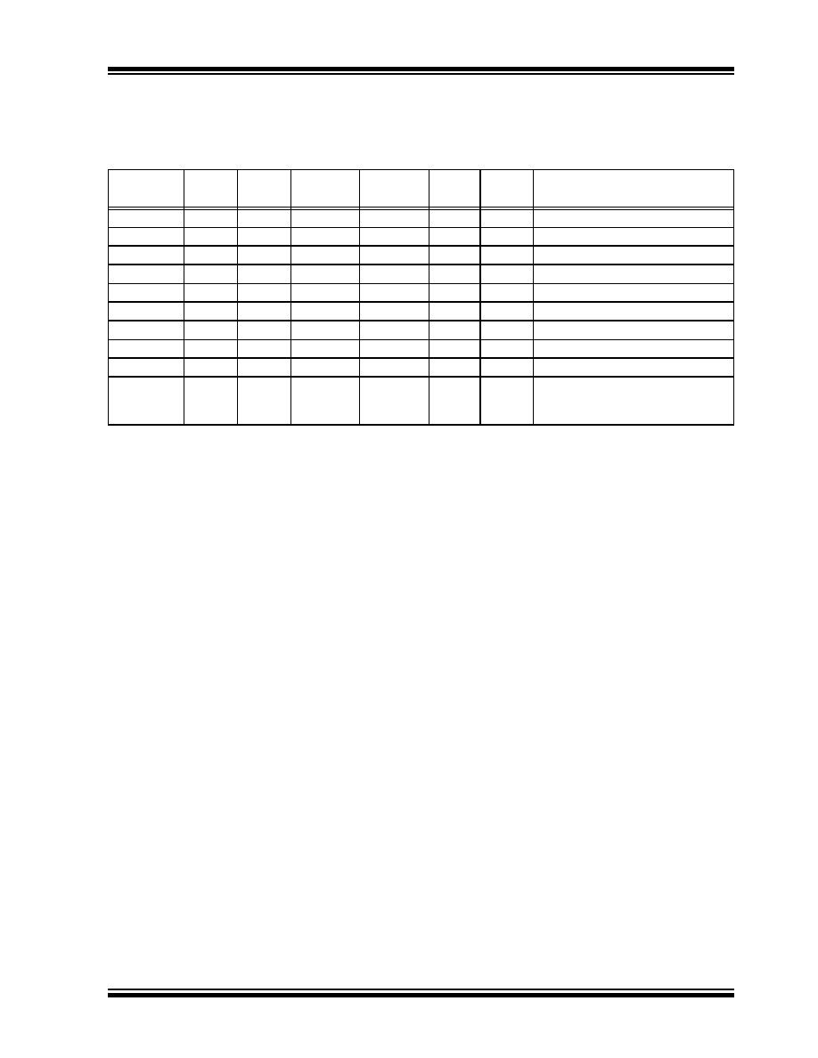
The descriptions of the pins are listed in Table 2-1.
TABLE 2-1:
PIN FUNCTION TABLE
2.1
A0, A1, A2 Chip Address Inputs
The A0, A1 and A2 inputs are used by the 24XX128 for
multiple device operations. The levels on these inputs
are compared with the corresponding bits in the slave
address. The chip is selected if the compare is true.
For the MSOP package only, pins A0 and A1 are not
connected.
Up to eight devices (two for the MSOP package) may
be connected to the same bus by using different Chip
Select bit combinations. If these pins are left uncon-
nected, the inputs will be pulled down internally to
V
SS
. If they are tied to V
CC
or driven high, the internal
pull-down circuitry is disabled.
In most applications, the chip address inputs A0, A1,
and A2 are hard-wired to logic `
0
' or logic `
1
'. For
applications in which these pins are controlled by a
microcontroller or other programmable device, the chip
address pins must be driven to logic `
0
' or logic `
1
'
before normal device operation can proceed.
2.2
Serial Data (SDA)
This is a bidirectional pin used to transfer addresses
and data into and out of the device. It is an open drain
terminal. Therefore, the SDA bus requires a pull-up
resistor to V
CC
(typical 10 k
for 100 kHz, 2 k
for
400 kHz and 1 MHz).
For normal data transfer, SDA is allowed to change
only during SCL low. Changes during SCL high are
reserved for indicating the Start and Stop conditions.
2.3
Serial Clock (SCL)
This input is used to synchronize the data transfer to
and from the device.
2.4
Write-Protect (WP)
This pin can be connected to either V
SS
, V
CC
or left
floating. Internal pull-down circuitry on this pin will keep
the device in the unprotected state if left floating. If tied
to V
SS
or left floating, normal memory operation is
enabled (read/write the entire memory
0000-3FFF).
If tied to V
CC
, write operations are inhibited. Read
operations are not affected.
3.0
FUNCTIONAL DESCRIPTION
The 24XX128 supports a bidirectional 2-wire bus and
data transmission protocol. A device that sends data
onto the bus is defined as a transmitter and a device
receiving data as a receiver. The bus must be
controlled by a master device which generates the
serial clock (SCL), controls the bus access and
generates the Start and Stop conditions while the
24XX128 works as a slave. Both master and slave can
operate as a transmitter or receiver, but the master
device determines which mode is activated.
Name
8-pin
PDIP
8-pin
SOIC
8-pin
TSSOP
14-pin
TSSOP
8-pin
MSOP
8-pin
DFN
Function
A0
1
1
1
1
--
1
User Configurable Chip Select
A1
2
2
2
2
--
2
User Configurable Chip Select
(NC)
--
--
--
3, 4, 5
1, 2
--
Not Connected
A2
3
3
3
6
3
3
User Configurable Chip Select
V
SS
4
4
4
7
4
4
Ground
SDA
5
5
5
8
5
5
Serial Data
SCL
6
6
6
9
6
6
Serial Clock
(NC)
--
--
--
10, 11,12
--
--
Not Connected
WP
7
7
7
13
7
7
Write-Protect Input
V
CC
8
8
8
14
8
8
+1.8V to 5.5V (24AA128)
+2.5V to 5.5V (24LC128)
+1.8V to 5.5V (24FC128)