 | –≠–ª–µ–∫—Ç—Ä–æ–Ω–Ω—ã–π –∫–æ–º–ø–æ–Ω–µ–Ω—Ç: 24FC65-P | –°–∫–∞—á–∞—Ç—å:  PDF PDF  ZIP ZIP |
©
1996 Microchip Technology Inc.
DS21125B-page 1
FEATURES
∑ Voltage operating range: 4.5V to 5.5V
- Maximum write current 3 mA at 5.5V
- Maximum read current 150
µ
A at 5.5V
- Standby current 1
µ
A typical
∑ 1 MHz SE2.bus two wire protocol
∑ Up to eight devices may be connected to the
same bus for up to 512K bits total memory
∑ Programmable block security options
∑ Programmable endurance options
∑ Schmitt trigger inputs for noise suppression
∑ Self-timed ERASE and WRITE cycles
∑ Power on/off data protection circuitry
∑ Endurance:
- 10,000,000 E/W cycles guaranteed for a 4K
block
- 1,000,000 E/W cycles guaranteed for a 60K
block
∑ Variable page size up to 64 bytes
∑ 8 byte x 8 line input cache (64 bytes)
for fast write loads
∑ <3 ms typical write cycle time, byte or page
∑ Electrostatic discharge protection > 4000V
∑ Data retention > 200 years
∑ 8-pin PDIP/SOIC packages
∑ Temperature ranges
DESCRIPTION
The Microchip Technology Inc. 24FC65 is a "smart"
8K 8x 8 Serial Electrically Erasable PROM (EEPROM)
with a high-speed 1MHz SE2.bus whose protocol is
functionally equivalent to the industry-standard I
2
C bus.
This device has been developed for advanced applica-
tions such as personal communications, and provides
the systems designer with flexibility through the use of
many new user-programmable features. The 24FC65
offers a relocatable 4K-bit block of ultra-high-endurance
memory for data that changes frequently. The remain-
der of the array, or 60K bits, is rated at 1,000,000
ERASE/WRITE (E/W) cycles guaranteed. The 24FC65
features an input cache for fast write loads with a
capacity of eight pages, or 64 bytes. This device also
features programmable security options for E/W pro-
- Commercial (C):
0
∞
C to +70
∞
C
- Industrial (I):
-40
∞
C to +85
∞
C
tection of critical data and/or code of up to fifteen 4K
blocks. Functional address lines allow the connection of
up to eight 24FC65's on the same bus for up to 512K bits
contiguous EEPROM memory. The 24FC65 is available
in the standard 8-pin plastic DIP and 8-pin surface
mount SOIC package.
24FC65
64K 5.0V 1 MHz I
2
C
TM
Smart Serial
TM
EEPROM
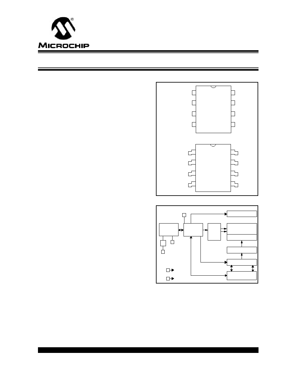
PACKAGE TYPES
BLOCK DIAGRAM
24FC65
A0
A1
A2
V
SS
1
2
3
4
8
7
6
5
V
CC
NC
SCL
SDA
24FC65
A0
A1
A2
V
SS
1
2
3
4
8
7
6
5
V
CC
NC
SCL
SDA
PDIP
SOIC
A0..A2
I/O
CONTROL
LOGIC
I/O
SDA
SCL
Vcc
Vss
MEMORY
CONTROL
LOGIC
XDEC
HV GENERATOR
EEPROM
ARRAY
PAGE LATCHES
YDEC
CACHE
SENSE AMP
R/W CONTROL
I
2
C is a trademark of Philips Corporation.
Smart Serial is a trademark of Microchip Technology Inc.
This document was created with FrameMaker 4 0 4
24FC65
DS21125B-page 2
©
1996 Microchip Technology Inc.
1.0
ELECTRICAL CHARACTERISTICS
1.1
Maximum Ratings*
V
CC
...................................................................................7.0V
All inputs and outputs w.r.t. V
SS
............... -0.6V to V
CC
+1.0V
Storage temperature .....................................-65
∞
C to +150
∞
C
Ambient temp. with power applied ................-65
∞
C to +125
∞
C
Soldering temperature of leads (10 seconds) ............. +300
∞
C
ESD protection on all pins
..................................................
4 kV
*Notice:
Stresses above those listed under "Maximum Ratings"
may cause permanent damage to the device. This is a stress rat-
ing only and functional operation of the device at those or any
other conditions above those indicated in the operational listings
of this specification is not implied. Exposure to maximum rating
conditions for extended periods may affect device reliability.
TABLE 1-1:
PIN FUNCTION TABLE
Name
Function
A0..A2
User Configurable Chip Selects
V
SS
Ground
SDA
Serial Address/Data I/O
SCL
Serial Clock
V
CC
+4.5V to 5.5V Power Supply
NC
No Internal Connection
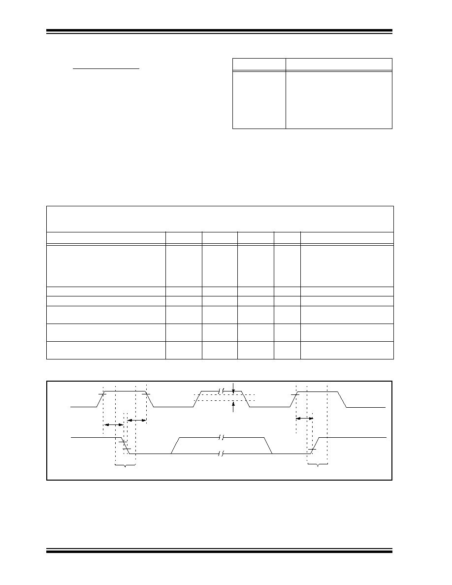
TABLE 1-2:
DC CHARACTERISTICS
FIGURE 1-1:
BUS TIMING START/STOP
V
CC
= +4.5V to +5.5V
Commercial (C): Tamb = 0
∞
C to +70
∞
C
Industrial (I):
Tamb = -40
∞
C to +85
∞
C
Parameter
Symbol
Min
Max
Units
Conditions
A0, A1, A2, SCL and SDA pins:
High level input voltage
Low level input voltage
Hysteresis of SCL and SDA
Low level output voltage of SDA
V
IH
V
IL
V
HYS
V
OL
0.7 V
CC
--
0.05 V
CC
--
--
0.3 Vcc
--
0.40
V
V
V
V
(Note)
I
OL
= 3.0 mA
Input leakage current
I
LI
-10
10
µ
A
V
IN
= 0.1V to V
CC
Output leakage current
I
LO
-10
10
µ
A
V
OUT
= 0.1V to V
CC
Pin capacitance
(all inputs/outputs)
C
INT
--
10
pF
V
CC
= 5.0V (Note)
Tamb = 25∞C, F
CLK
= 1 MHz
Operating current
I
CC
Write
I
CC
Read
--
--
3
150
mA
µ
A
V
CC
= 5.5V, SCL = 1 MH
Z
V
CC
= 5.5V, SCL = 1 MHz
Standby current
I
CCS
--
5
(1 typical)
µ
A
V
CC
= 5.5V, SCL = SDA =V
CC
(Note)
Note:
This periodically sampled and not 100% tested.
SCL
SDA
START
STOP
V
HYS
T
SU
:
STO
T
HD
:
STA
T
SU
:
STA
This document was created with FrameMaker 4 0 4
©
1996 Microchip Technology Inc.
DS21125B-page 3
24FC65
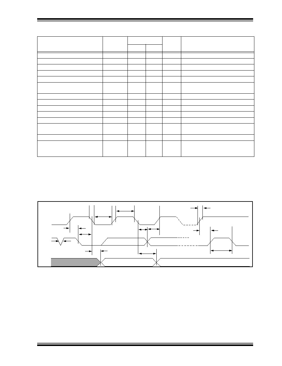
TABLE 1-3:
AC CHARACTERISTICS
FIGURE 1-2:
BUS TIMING DATA
Parameter
Symbol
1 MHz Bus
Units
Remarks
Min
Max
Clock frequency
F
CLK
0
1000
kHz
Clock high time
THIGH
500
--
ns
Clock low time
T
LOW
500
--
ns
SDA and SCL rise time
T
R
--
300
ns
(Note 1)
SDA and SCL fall time
T
F
--
100
ns
(Note 1)
START hold time
T
HD
:
STA
250
--
ns
After this period the first clock pulse is
generated
START setup time
T
SU
:
STA
250
--
ns
Only relevant for repeated START
Data input hold time
T
HD
:
DAT
0
--
ns
Data input setup time
T
SU
:
DAT
100
--
ns
STOP setup time
T
SU
:
STO
250
--
ns
Output valid from clock
T
AA
--
350
ns
(Note 2)
Bus free time
T
BUF
500
--
ns
Time the bus must be free before a
new transmission can start
Write cycle time
T
WR
--
5
ms/page (Note 3)
Endurance
High Endurance Block
Rest of Array
10M
1M
--
--
cycles
25
∞
C, Vcc = 5.0V, Block Mode (Note 4)
Note 1: Not 100 percent tested.
2: As a transmitter, the device must provide an internal minimum delay time to bridge the undefined region (min-
imum 100 ns) of the falling edge of SCL to avoid unintended generation of START or STOPs.
3: The times shown are for a single page of 8 bytes. Multiply by the number of pages loaded into the write cache
for total time.
4: This parameter is not tested but guaranteed by characterization. For endurance estimates in a specific appli-
cation, please consult the Total Endurance Model which can be obtained on our BBS or website.
SCL
SDA
IN
SDA
OUT
T
SU
:
STA
T
SP
T
AA
T
F
T
LOW
T
HIGH
T
HD
:
STA
T
HD
:
DAT
T
SU
:
DAT
T
SU
:
STO
T
BUF
T
AA
T
R
24FC65
DS21125B-page 4
©
1996 Microchip Technology Inc.
2.0
FUNCTIONAL DESCRIPTION
The 24FC65 supports a bidirectional two-wire bus and
data transmission protocol. A device that sends data
onto the bus is defined as transmitter, and a device
receiving data as receiver. The bus must be controlled
by a master device which generates the serial clock
(SCL), controls the bus access, and generates the
START and STOPs, while the 24FC65 works as slave.
Both master and slave can operate as transmitter or
receiver but the master device determines which mode
is activated.
3.0
BUS CHARACTERISTICS
The following
bus protocol has been defined:
∑ Data transfer may be initiated only when the bus is
not busy.
∑ During data transfer, the data line must remain
stable whenever the clock line is HIGH. Changes
in the data line while the clock line is HIGH will be
interpreted as a START or STOP.
Accordingly, the following bus conditions have been
defined (Figure 3-1).
3.1
Bus not Busy (A)
Both data and clock lines remain HIGH.
3.2
Start Data Transfer (B)
A HIGH to LOW transition of the SDA line while the
clock (SCL) is HIGH determines a START. All
commands must be preceded by a START.
3.3
Stop Data Transfer (C)
A LOW to HIGH transition of the SDA line while the
clock (SCL) is HIGH determines a STOP. All operations
must be ended with a STOP.
3.4
Data Valid (D)
The state of the data line represents valid data when,
after a START, the data line is stable for the duration of
the HIGH period of the clock signal.
The data on the line must be changed during the LOW
period of the clock signal. There is one clock pulse per
bit of data.
Each data transfer is initiated with a START and
terminated with a STOP. The number of the data bytes
transferred between the START and STOPs is
determined by the master device.
3.5
Acknowledge
Each receiving device, when addressed, is obliged to
generate an acknowledge after the reception of each
byte. The master device must generate an extra clock
pulse which is associated with this acknowledge bit.
A device that acknowledges must pull down the SDA
line during the acknowledge clock pulse in such a way
that the SDA line is stable LOW during the HIGH period
of the acknowledge related clock pulse. Of course,
setup and hold times must be taken into account.
During reads, a master must signal an end of data to
the slave by NOT generating an acknowledge bit on the
last byte that has been clocked out of the slave. In this
case, the slave (24FC65) must leave the data line
HIGH to enable the master to generate the STOP.
Note:
The 24FC65 does not generate any
acknowledge bits if an internal program-
ming cycle is in progress.
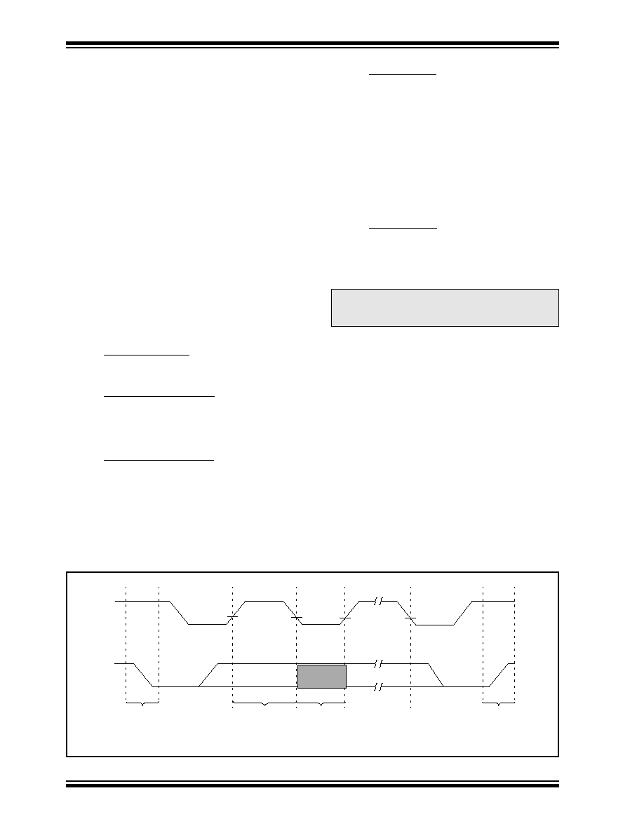
FIGURE 3-1:
DATA TRANSFER SEQUENCE ON THE SERIAL BUS
SCL
SDA
(A)
(B)
START
(C)
(A)
(D)
(D)
Address
or
Acknowledge
Valid
Data Allowed
to Change
STOP
Condition
Condition
©
1996 Microchip Technology Inc.
DS21125B-page 5
24FC65
3.6
Device Addressing
A control byte is the first byte received following the
START from the master device. The control byte consists
of a four bit control code, for the 24FC65 this is set as
1010 binary for read and write operations. The next three
bits of the control byte are the device select bits (A2, A1,
A0). They are used by the master device to select which
of the eight devices are to be accessed. These bits are
in effect the three most significant bits of the word
address. The last bit of the control byte (R/W) defines the
operation to be performed. When set to a one a read
operation is selected, when set to a zero a write opera-
tion is selected. The next two bytes received define the
address of the first data byte (Figure 4-1). Because only
A12..A0 are used, the upper three address bits must be
zeros. The most significant bit of the most significant byte
is transferred first. Following the START, the 24FC65
monitors the SDA bus checking the device type identifier
being transmitted. Upon receiving a 1010 code and
appropriate device select bits, the slave device (24FC65)
outputs an acknowledge signal on the SDA line.
Depending upon the state of the R/W bit, the 24FC65 will
select a read or write operation.
FIGURE 3-2:
CONTROL BYTE
ALLOCATION
Operation
Control
Code
Device Select
R/W
Read
1010
Device Address
1
Write
1010
Device Address
0
SLAVE ADDRESS
X = Don't care
1
0
1
0
A2
A1
A0
R/W
A
START
READ/WRITE
4.0
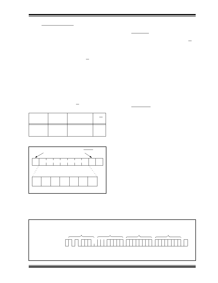
WRITE OPERATION
4.1
Byte Write
Following the START from the master, the control code
(four bits), the device select (three bits), and the R/W bit
which is a logic low is placed onto the bus by the master
transmitter. This indicates to the addressed slave
receiver (24FC65) that a byte with a word address will
follow after it has generated an acknowledge bit during
the ninth clock cycle. Therefore the next byte transmitted
by the master is the high-order byte of the word address
and will be written into the address pointer of the
24FC65. The next byte is the least significant address
byte. After receiving another acknowledge signal from
the 24FC65 the master device will transmit the data word
to be written into the addressed memory location. The
24FC65 acknowledges again and the master generates
a STOP. This initiates the internal write cycle, and during
this time the 24FC65 will not generate acknowledge sig-
nals (Figure 4-1).
4.2
Page Write
The write control byte, word address and the first data
byte are transmitted to the 24FC65 in the same way as
in a byte write. But instead of generating a STOP the
master transmits up to eight pages of eight data bytes
each (64 bytes total) which are temporarily stored in the
on-chip page cache of the 24FC65. They will be written
from the cache into the EEPROM array after the master
has transmitted a STOP. After the receipt of each word,
the six lower order address pointer bits are internally
incremented by one. The higher order seven bits of the
word address remain constant. If the master should
transmit more than eight bytes prior to generating the
STOP (writing across a page boundary), the address
counter (lower three bits) will roll over and the pointer will
be incremented to point to the next line in the cache. This
can continue to occur up to eight times or until the cache
is full, at which time a STOP should be generated by the
master. If a STOP is not received, the cache pointer will
roll over to the first line (byte 0) of the cache, and any
further data received will overwrite previously captured
data. The STOP can be sent at any time during the
transfer. As with the byte write operation, once the STOP
is received an internal write cycle will begin. The 64 byte
cache will continue to capture data until a STOP occurs
or the operation is aborted (Figure 4-2).
FIGURE 4-1:
BYTE WRITE
BUS ACTIVITY
MASTER
SDA LINE
BUS ACTIVITY
CONTROL
BYTE
WORD
ADDRESS (1)
A
C
K
S
T
A
R
T
WORD
ADDRESS (0)
A
C
K
A
C
K
0
S
T
O
P
A
C
K
0 0
DATA