 | –≠–ª–µ–∫—Ç—Ä–æ–Ω–Ω—ã–π –∫–æ–º–ø–æ–Ω–µ–Ω—Ç: 25LC010A | –°–∫–∞—á–∞—Ç—å:  PDF PDF  ZIP ZIP |

©
2006 Microchip Technology Inc.
Preliminary
DS21832C-page 1
25AA010A/25LC010A
Device Selection Table
Features:
∑ 10 MHz max. clock frequency
∑ Low-power CMOS technology:
- Max. Write Current: 5 mA at 5.5V, 10 MHz
- Read Current: 5 mA at 5.5V, 10 MHz
- Standby Current: 5
A at 5.5V
∑ 128 x 8-bit organization
∑ Write Page mode (up to 16 bytes)
∑ Sequential Read
∑ Self-timed Erase and Write cycles (5 ms max.)
∑ Block Write protection:
- Protect none, 1/4, 1/2 or all of array
∑ Built-in Write protection:
- Power-on/off data protection circuitry
- Write enable latch
- Write-protect pin
∑ High reliability:
- Endurance: 1,000,000 Erase/Write cycles
- Data retention: > 200 years
- ESD protection: > 4000V
∑ Temperature ranges supported:
∑ Pb-Free packages available
Pin Function Table
Description:
The Microchip Technology Inc. 25XX010A* is a 1 Kbit
Serial Electrically Erasable Programmable Read-Only
Memory (EEPROM). The memory is accessed via a
simple Serial Peripheral InterfaceTM (SPI) compatible
serial bus. The bus signals required are a clock input
(SCK) plus separate data in (SI) and data out (SO)
lines. Access to the device is controlled through a Chip
Select (CS) input.
Communication to the device can be paused via the
hold pin (HOLD). While the device is paused,
transitions on its inputs will be ignored, with the
exception of Chip Select, allowing the host to service
higher priority interrupts.
The 25XX010A is available in standard packages
including 8-lead PDIP and SOIC, and advanced
packages including 8-lead MSOP, 8-lead TSSOP and
rotated TSSOP, 8-lead 2x3 DFN, and 6-lead SOT-23.
Package Types (not to scale)
Part Number
V
CC
Range
Page Size
Temp. Ranges
Packages
25AA010A
1.8-5.5V
16 Bytes
I
P, MS, SN, ST, MC, OT
25LC010A
2.5-5.5V
16 Bytes
I, E
P, MS, SN, ST, MC, OT
- Industrial (I):
-40
∞
C to
+85
∞
C
- Automotive (E):
-40
∞
C to +125
∞
C
Name
Function
CS
Chip Select Input
SO
Serial Data Output
WP
Write-Protect
V
SS
Ground
SI
Serial Data Input
SCK
Serial Clock Input
HOLD
Hold Input
V
CC
Supply Voltage
CS
SO
WP
V
SS
1
2
3
4
8
7
6
5
V
CC
HOLD
SCK
SI
(P, SN)
V
SS
1
2
3
4
6
5
V
DD
CS
SO
(OT)
PDIP/SOIC
X-Rotated TSSOP
HOLD
V
CC
CS
SO
1
2
3
4
8
7
6
5
SCK
SI
V
SS
WP
(X/ST)
CS
SO
WP
V
SS
1
2
3
4
8
7
6
5
V
CC
HOLD
SCK
SI
CS
SO
WP
V
SS
1
2
3
4
8
7
6
5
V
CC
HOLD
SCK
SI
(ST, MS)
TSSOP/MSOP
SOT-23
SCK
SI
CS
SO
WP
V
SS
1
2
3
4
8
7
6
5
V
CC
HOLD
SCK
SI
(MC)
DFN
1K SPI Bus Serial EEPROM
*25XX010A is used in this document as a generic part number for the
25AA010A and the 25LC010A.

25AA010A/25LC010A
DS21832C-page 2
Preliminary
©
2006 Microchip Technology Inc.
1.0
ELECTRICAL CHARACTERISTICS
Absolute Maximum Ratings
()
V
CC
.............................................................................................................................................................................6.5V
All inputs and outputs w.r.t. V
SS
......................................................................................................... -0.6V to V
CC
+1.0V
Storage temperature .................................................................................................................................-65∞C to 150∞C
Ambient temperature under bias ...............................................................................................................-40∞C to 125∞C
ESD protection on all pins .......................................................................................................................................... 4 kV
TABLE 1-1:
DC CHARACTERISTICS
NOTICE: Stresses above those listed under "Absolute Maximum Ratings" may cause permanent damage to the
device. This is a stress rating only and functional operation of the device at those or any other conditions above those
indicated in the operational listings of this specification is not implied. Exposure to maximum rating conditions for an
extended period of time may affect device reliability.
DC CHARACTERISTICS
Industrial (I):
T
A
= -40∞C to +85∞C
V
CC
= 1.8V to 5.5V
Automotive (E):
T
A
= -40∞C to +125∞C
V
CC
= 2.5V to 5.5V
Param.
No.
Sym.
Characteristic
Min.
Max.
Units
Test Conditions
D001
V
IH1
High-level Input
Voltage
0.7 V
CC
V
CC
+1
V
D002
V
IL1
Low-level Input
Voltage
-0.3
0.3 V
CC
V
V
CC
2.7V (Note)
D003
V
IL2
-0.3
0.2 V
CC
V
V
CC
< 2.7V (Note)
D004
V
OL
Low-level Output
Voltage
--
0.4
V
I
OL
= 2.1 mA
D005
V
OL
--
0.2
V
I
OL
= 1.0 mA, V
CC
< 2.5V
D006
V
OH
High-level Output
Voltage
V
CC
-0.5
--
V
I
OH
= -400
A
D007
I
LI
Input Leakage
Current
--
±1
A
CS = V
CC
, V
IN
= V
SS
TO
V
CC
D008
I
LO
Output Leakage
Current
--
±1
A
CS = V
CC
, V
OUT
= V
SS
TO
V
CC
D009
C
INT
Internal Capacitance
(all inputs and
outputs)
--
7
pF
T
A
= 25∞C, CLK = 1.0 MHz,
V
CC
= 5.0V (Note)
D010
I
CC
Read
Operating Current
--
--
5
2.5
mA
mA
V
CC
= 5.5V; F
CLK
= 10.0 MHz;
SO = Open
V
CC
= 2.5V; F
CLK
= 5.0 MHz;
SO = Open
D011
I
CC
Write
--
--
5
3
mA
mA
V
CC
= 5.5V
V
CC
= 2.5V
D012
I
CCS
Standby Current
--
--
5
1
A
A
CS = V
CC
= 5.5V, Inputs tied to V
CC
or
V
SS
, T
A
= +125∞C
CS = V
CC
= 2.5V, Inputs tied to V
CC
or
V
SS
, T
A
= +85∞C
Note:
This parameter is periodically sampled and not 100% tested.

©
2006 Microchip Technology Inc.
Preliminary
DS21832C-page 3
25AA010A/25LC010A
TABLE 1-2:
AC CHARACTERISTICS
AC CHARACTERISTICS
Industrial (I):
T
A
= -40∞C to +85∞C
V
CC
= 1.8V to 5.5V
Automotive (E): T
A
= -40∞C to +125∞C
V
CC
= 2.5V to 5.5V
Param.
No.
Sym.
Characteristic
Min.
Max.
Units
Test Conditions
1
F
CLK
Clock Frequency
--
--
--
10
5
3
MHz
MHz
MHz
4.5V
V
CC
<
5.5V
2.5V
V
CC
<
4.5V
1.8V
V
CC
<
2.5V
2
T
CSS
CS Setup Time
50
100
150
--
--
--
ns
ns
ns
4.5V
V
CC
<
5.5V
2.5V
V
CC
<
4.5V
1.8V
V
CC
<
2.5V
3
T
CSH
CS Hold Time
100
200
250
--
--
--
ns
ns
ns
4.5V
V
CC
<
5.5V
2.5V
V
CC
<
4.5V
1.8V
V
CC
<
2.5V
4
T
CSD
CS Disable Time
50
--
ns
--
5
Tsu
Data Setup Time
10
20
30
--
--
--
ns
ns
ns
4.5V
V
CC
<
5.5V
2.5V
V
CC
<
4.5V
1.8V
V
CC
<
2.5V
6
T
HD
Data Hold Time
20
40
50
--
--
--
ns
ns
ns
4.5V
V
CC
<
5.5V
2.5V
V
CC
<
4.5V
1.8V
V
CC
<
2.5V
7
T
R
CLK Rise Time
--
2
s
(Note 1)
8
T
F
CLK Fall Time
--
2
s
(Note 1)
9
T
HI
Clock High Time
0.05
0.1
0.15
1000
1000
1000
s
s
s
4.5V
V
CC
<
5.5V
2.5V
V
CC
<
4.5V
1.8V
V
CC
<
2.5V
10
T
LO
Clock Low Time
0.05
0.1
0.15
1000
1000
1000
s
s
s
4.5V
V
CC
<
5.5V
2.5V
V
CC
<
4.5V
1.8V
V
CC
<
2.5V
11
T
CLD
Clock Delay Time
50
--
ns
--
12
T
CLE
Clock Enable Time
50
--
ns
--
13
T
V
Output Valid from Clock
Low
--
--
--
50
100
160
ns
ns
ns
4.5V
V
CC
<
5.5V
2.5V
V
CC
<
4.5V
1.8V
V
CC
<
2.5V
14
T
HO
Output Hold Time
0
--
ns
(Note 1)
15
T
DIS
Output Disable Time
--
--
--
40
80
160
ns
ns
ns
4.5V
V
CC
<
5.5V (Note 1)
2.5V
V
CC
<
4.5V (Note 1)
1.8V
V
CC
<
2.5V (Note 1)
16
T
HS
HOLD Setup Time
20
40
80
--
--
--
ns
ns
ns
4.5V
V
CC
<
5.5V
2.5V
V
CC
<
4.5V
1.8V
V
CC
<
2.5V
Note 1: This parameter is periodically sampled and not 100% tested.
2: This parameter is not tested but ensured by characterization. For endurance estimates in a specific
application, please consult the Total EnduranceTM Model which can be obtained from our web site:
www.microchip.com.
3: T
WC
begins on the rising edge of CS after a valid write sequence and ends when the internal write cycle
is complete.

25AA010A/25LC010A
DS21832C-page 4
Preliminary
©
2006 Microchip Technology Inc.
TABLE 1-3:
AC TEST CONDITIONS
17
T
HH
HOLD Hold Time
20
40
80
--
--
--
ns
ns
ns
4.5V
V
CC
<
5.5V
2.5V
V
CC
<
4.5V
1.8V
V
CC
<
2.5V
18
T
HZ
HOLD Low to Output
High-Z
30
60
160
--
--
--
ns
ns
ns
4.5V
V
CC
<
5.5V (Note 1)
2.5V
V
CC
<
4.5V (Note 1)
1.8V
V
CC
<
2.5V (Note 1)
19
T
HV
HOLD High to Output
Valid
30
60
160
--
--
--
ns
ns
ns
4.5V
V
CC
<
5.5V
2.5V
V
CC
<
4.5V
1.8V
V
CC
<
2.5V
20
T
WC
Internal Write Cycle Time
(byte or page)
--
5
ms
(N
OTE
3)
21
--
Endurance
1M
--
E/W
Cycles
(N
OTE
2)
TABLE 1-2:
AC CHARACTERISTICS (CONTINUED)
AC CHARACTERISTICS
Industrial (I):
T
A
= -40∞C to +85∞C
V
CC
= 1.8V to 5.5V
Automotive (E): T
A
= -40∞C to +125∞C
V
CC
= 2.5V to 5.5V
Param.
No.
Sym.
Characteristic
Min.
Max.
Units
Test Conditions
Note 1: This parameter is periodically sampled and not 100% tested.
2: This parameter is not tested but ensured by characterization. For endurance estimates in a specific
application, please consult the Total EnduranceTM Model which can be obtained from our web site:
www.microchip.com.
3: T
WC
begins on the rising edge of CS after a valid write sequence and ends when the internal write cycle
is complete.
AC Waveform:
V
LO
= 0.2V
--
V
H I
= V
CC
- 0.2V
(Note 1)
V
H I
= 4.0V
(Note 2)
C
L
= 100 pF
--
Timing Measurement Reference Level
Input
0.5 V
CC
Output
0.5 V
CC
Note 1: For V
CC
4.0V
2: For V
CC
>
4.0V

©
2006 Microchip Technology Inc.
Preliminary
DS21832C-page 5
25AA010A/25LC010A
FIGURE 1-1:
HOLD TIMING
FIGURE 1-2:
SERIAL INPUT TIMING
FIGURE 1-3:
SERIAL OUTPUT TIMING
CS
SCK
SO
SI
HOLD
17
16
16
17
19
18
don't care
5
high-impedance
n + 2
n + 1
n
n - 1
n
n + 2
n + 1
n
n
n - 1
CS
SCK
SI
SO
6
5
8
7
11
3
LSB in
MSB in
high-impedance
12
Mode 1,1
Mode 0,0
2
4
CS
SCK
SO
10
9
13
MSB out
ISB out
3
15
don't care
SI
Mode 1,1
Mode 0,0
14

25AA010A/25LC010A
DS21832C-page 6
Preliminary
©
2006 Microchip Technology Inc.
2.0
FUNCTIONAL DESCRIPTION
2.1
Principles of Operation
The 25XX010A is a 128 byte Serial EEPROM designed
to interface directly with the Serial Peripheral Interface
(SPI) port of many of today's popular microcontroller
families, including Microchip's PICmicro
Æ
microcontrol-
lers. It may also interface with microcontrollers that do
not have a built-in SPI port by using discrete I/O lines
programmed properly in firmware to match the SPI
protocol.
The 25XX010A contains an 8-bit instruction register.
The device is accessed via the SI pin, with data being
clocked in on the rising edge of SCK. The CS pin must
be low and the HOLD pin must be high for the entire
operation.
Table 2-1 contains a list of the possible instruction
bytes and format for device operation. All instructions,
addresses, and data are transferred MSb first, LSb last.
Data (SI) is sampled on the first rising edge of SCK
after CS goes low. If the clock line is shared with other
peripheral devices on the SPI bus, the user can assert
the HOLD input and place the 25XX010A in `HOLD'
mode. After releasing the HOLD pin, operation will
resume from the point when the HOLD was asserted.
2.2
Read Sequence
The device is selected by pulling CS low. The 8-bit
READ
instruction is transmitted to the 25XX010A
followed by an 8-bit address. See Figure 2-1 for more
details.
After the correct
READ
instruction and address are sent,
the data stored in the memory at the selected address
is shifted out on the SO pin. Data stored in the memory
at the next address can be read sequentially by
continuing to provide clock pulses to the slave. The
internal Address Pointer automatically increments to
the next higher address after each byte of data is
shifted out. When the highest address is reached
(7Fh), the address counter rolls over to address 00h
allowing the read cycle to be continued indefinitely. The
read operation is terminated by raising the CS pin
(Figure 2-1).
2.3
Write Sequence
Prior to any attempt to write data to the 25XX010A, the
write enable latch must be set by issuing the
WREN
instruction (Figure 2-4). This is done by setting CS low
and then clocking out the proper instruction into the
25XX010A. After all eight bits of the instruction are
transmitted, CS must be driven high to set the write
enable latch. If the write operation is initiated immedi-
ately after the
WREN
instruction without CS driven high,
data will not be written to the array since the write
enable latch was not properly set.
After setting the write enable latch, the user may
proceed by driving CS low, issuing a
WRITE
instruction,
followed by the remainder of the address, and then the
data to be written. Up to 16 bytes of data can be sent to
the device before a write cycle is necessary. The only
restriction is that all of the bytes must reside in the
same page. Additionally, a page address begins with
XXXX 0000
and ends with
XXXX 1111
. If the internal
address counter reaches
XXXX 1111
and clock signals
continue to be applied to the chip, the address counter
will roll back to the first address of the page and over-
write any data that previously existed in those
locations.
For the data to be actually written to the array, the CS
must be brought high after the Least Significant bit (D0)
of the n
th
data byte has been clocked in. If CS is driven
high at any other time, the write operation will not be
completed. Refer to Figure 2-2 and Figure 2-3 for more
detailed illustrations on the byte write sequence and
the page write sequence, respectively. While the write
is in progress, the STATUS register may be read to
check the status of the WIP, WEL, BP1 and BP0 bits
(Figure 2-6). Attempting to read a memory array
location will not be possible during a write cycle. Polling
the WIP bit in the STATUS register is recommended in
order to determine if a write cycle is in progress. When
the write cycle is completed, the write enable latch is
reset.
Note:
Page write operations are limited to writing
bytes within a single physical page,
regardless of the number of bytes
actually being written. Physical page
boundaries start at addresses that are
integer multiples of the page buffer size (or
`page size') and, end at addresses that are
integer multiples of page size ≠ 1. If a
Page Write command attempts to write
across a physical page boundary, the
result is that the data wraps around to the
beginning of the current page (overwriting
data previously stored there), instead of
being written to the next page as might be
expected. It is therefore necessary for the
application software to prevent page write
operations that would attempt to cross a
page boundary.
©
2006 Microchip Technology Inc.
Preliminary
DS21832C-page 7
25AA010A/25LC010A
BLOCK DIAGRAM
FIGURE 2-1:
READ SEQUENCE
SI
SO
SCK
CS
HOLD
WP
STATUS
Register
I/O Control
Memory
Control
Logic
X
Dec
HV Generator
EEPROM
Array
Page Latches
Y Decoder
Sense Amp.
R/W Control
Logic
V
CC
V
SS
TABLE 2-1:
INSTRUCTION SET
Instruction Name
Instruction Format
Description
READ
0000 x011
Read data from memory array beginning at selected address
WRITE
0000 x010
Write data to memory array beginning at selected address
WRDI
0000 x100
Reset the write enable latch (disable write operations)
WREN
0000 x110
Set the write enable latch (enable write operations)
RDSR
0000 x101
Read STATUS register
WRSR
0000 x001
Write STATUS register
x
= don't care
SO
SI
SCK
CS
0
2
3
4
5
6
7
8
9 10 11
1
0
1
0
0
0
0
0
1
X
A
6
A
5
A
4
A
1
A
0
7
6
5
4
3
2
1
0
data out
high-impedance
A
3
A
2
Address byte
12 13 14 15 16 17 18 19 20 21 22 23
Instruction

25AA010A/25LC010A
DS21832C-page 8
Preliminary
©
2006 Microchip Technology Inc.
FIGURE 2-2:
BYTE WRITE SEQUENCE
X
= don't care
FIGURE 2-3:
PAGE WRITE SEQUENCE
X
= don't care
SO
SI
CS
0
2
3
4
5
6
7
8
9 10 11
1
0
0
0
0
0
0
0
1
X
A
6
A
5
A
4
A
1
A
3
A
2
Address byte
12 13 14 15 16 17 18 19 20 21 22 23
Instruction
data byte
A
0
6
7
5
4
3
2
1
0
high-impedance
Twc
SCK
SI
CS
9 10 11
0
0
0
0
0
0
0
1
7
6
5
4
3
2
1
0
data byte 1
SCK
0
2
3
4
5
6
7
1
8
SI
CS
33 34 35
38 39
7
6
5
4
3
2
1
0
data byte n (16 max)
SCK
24
26 27 28 29 30 31
25
32
7
6
5
4
3
2
1
0
data byte 3
7
6
5
4
3
2
1
0
data byte 2
36 37
Instruction
Address byte
X
A
6
A
5
A
4
A
3
A
1
A
0
A
2
12 13 14 15 16 17 18 19 20 21 22 23

©
2006 Microchip Technology Inc.
Preliminary
DS21832C-page 9
25AA010A/25LC010A
2.4
Write Enable (
WREN
) and Write
Disable (
WRDI
)
The 25XX010A contains a write enable latch. See
Table 2-4 for the Write-Protect Functionality Matrix.
This latch must be set before any write operation will be
completed internally. The
WREN
instruction will set the
latch, and the
WRDI
will reset the latch.
The following is a list of conditions under which the
write enable latch will be reset:
∑ Power-up
∑
WRDI
instruction successfully executed
∑
WRSR
instruction successfully executed
∑
WRITE
instruction successfully executed
∑ WP pin is brought low
FIGURE 2-4:
WRITE ENABLE SEQUENCE (
WREN
)
FIGURE 2-5:
WRITE DISABLE SEQUENCE (
WRDI
)
SCK
0
2
3
4
5
6
7
1
SI
high-impedance
SO
CS
0
1
0
0
0
0
0
1
SCK
0
2
3
4
5
6
7
1
SI
high-impedance
SO
CS
0
1
0
0
0
0
0
0

25AA010A/25LC010A
DS21832C-page 10
Preliminary
©
2006 Microchip Technology Inc.
2.5
Read Status Register Instruction
(
RDSR
)
The Read Status Register instruction (
RDSR
) provides
access to the STATUS register. See Figure 2-6 for the
RDSR
timing sequence. The STATUS register may be
read at any time, even during a write cycle. The STA-
TUS register is formatted as follows:
TABLE 2-2:
STATUS REGISTER
The Write-In-Process (WIP) bit indicates whether the
25XX010A is busy with a write operation. When set to
a `
1
', a write is in progress, when set to a `
0
', no write
is in progress. This bit is read-only.
The Write Enable Latch (WEL) bit indicates the status
of the write enable latch and is read-only. When set to
a `
1
', the latch allows writes to the array, when set to a
`
0
', the latch prohibits writes to the array. The state of
this bit can always be updated via the
WREN
or
WRDI
commands regardless of the state of write protection
on the STATUS register. These commands are shown
in Figure 2-4 and Figure 2-5.
The Block Protection (BP0 and BP1) bits indicate
which blocks are currently write-protected. These bits
are set by the user issuing the
WRSR
instruction, which
is shown in Figure 2-7. These bits are nonvolatile and
are described in more detail in Table 2-3.
FIGURE 2-6:
READ STATUS REGISTER TIMING SEQUENCE (
RDSR
)
7
6
5
4
3
2
1
0
≠
≠
≠
≠
W/R
W/R
R
R
X
X
X
X
BP1
BP0
WEL
WIP
W/R = writable/readable. R = read-only.
SO
SI
CS
9
10
11
12
13
14
15
1
1
0
0
0
0
0
0
7
6
5
4
2
1
0
instruction
data from STATUS register
high-impedance
SCK
0
2
3
4
5
6
7
1
8
3

©
2006 Microchip Technology Inc.
Preliminary
DS21832C-page 11
25AA010A/25LC010A
2.6
Write Status Register Instruction
(
WRSR
)
The Write Status Register instruction (
WRSR
) allows the
user to write to the nonvolatile bits in the STATUS reg-
ister as shown in Table 2-2. See Figure 2-7 for the
WRSR
timing sequence. Four levels of protection for the
array are selectable by writing to the appropriate bits in
the STATUS register. The user has the ability to write-
protect none, one, two or all four of the segments of the
array as shown in Table 2-3.
TABLE 2-3:
ARRAY PROTECTION
FIGURE 2-7:
WRITE STATUS REGISTER TIMING SEQUENCE (
WRSR
)
BP1
BP0
Array Addresses
Write-Protected
0
0
none
0
1
upper 1/4
(60h-7Fh)
1
0
upper 1/2
(40h-7Fh)
1
1
all
(00h-7Fh)
SO
SI
CS
9
10
11
12
13
14
15
0
1
0
0
0
0
0
0
7
6
5
4
2
1
0
instruction
data to STATUS register
high-impedance
SCK
0
2
3
4
5
6
7
1
8
3
Note:
An internal write cycle (T
WC
) is initiated on the rising edge of CS after a valid write STATUS register
sequence.
25AA010A/25LC010A
DS21832C-page 12
Preliminary
©
2006 Microchip Technology Inc.
2.7
Data Protection
The following protection has been implemented to
prevent inadvertent writes to the array:
∑ The write enable latch is reset on power-up
∑ A write enable instruction must be issued to set
the write enable latch
∑ After a byte write, page write or STATUS register
write, the write enable latch is reset
∑ CS must be set high after the proper number of
clock cycles to start an internal write cycle
∑ Access to the array during an internal write cycle
is ignored and programming is continued
2.8
Power-On State
The 25XX010A powers on in the following state:
∑ The device is in low-power Standby mode
(CS =
1
)
∑ The write enable latch is reset
∑ SO is in high-impedance state
∑ A high-to-low-level transition on CS is required to
enter active state
TABLE 2-4:
WRITE-PROTECT FUNCTIONALITY MATRIX
WP
(pin 3)
WEL
(SR bit 1)
Protected Blocks
Unprotected Blocks
Status Register
0
(low)
x
Protected
Protected
Protected
1
(high)
0
Protected
Protected
Protected
1
(high)
1
Protected
Writable
Writable
x
= don't care
©
2006 Microchip Technology Inc.
Preliminary
DS21832C-page 13
25AA010A/25LC010A
3.0
PIN DESCRIPTIONS
The descriptions of the pins are listed in Table 3-1.
TABLE 3-1:
PIN FUNCTION TABLE
3.1
Chip Select (CS)
A low level on this pin selects the device. A high level
deselects the device and forces it into Standby mode.
However, a programming cycle which is already
initiated or in progress will be completed, regardless of
the CS input signal. If CS is brought high during a
program cycle, the device will go into Standby mode as
soon as the programming cycle is complete. When the
device is deselected, SO goes to the high-impedance
state, allowing multiple parts to share the same SPI
bus. A low-to-high transition on CS after a valid write
sequence initiates an internal write cycle. After power-
up, a low level on CS is required prior to any sequence
being initiated.
3.2
Serial Output (SO)
The SO pin is used to transfer data out of the
25XX010A. During a read cycle, data is shifted out on
this pin after the falling edge of the serial clock.
3.3
Write-Protect (WP)
The WP pin is a hardware write-protect input pin.
When it is low, all writes to the array or STATUS reg-
ister are disabled, but any other operations function
normally. When WP is high, all functions, including
nonvolatile writes operate normally. At any time, when
WP is low, the write enable reset latch will be reset
and programming will be inhibited. However, if a write
cycle is already in progress, WP going low will not
change or disable the write cycle. See Table 2-4 for
the Write-Protect Functionality Matrix.
3.4
Serial Input (SI)
The SI pin is used to transfer data into the device. It
receives instructions, addresses and data. Data is
latched on the rising edge of the serial clock.
3.5
Serial Clock (SCK)
The SCK is used to synchronize the communication
between a master and the 25XX010A. Instructions,
addresses or data present on the SI pin are latched on
the rising edge of the clock input, while data on the SO
pin is updated after the falling edge of the clock input.
3.6
Hold (HOLD)
The HOLD pin is used to suspend transmission to the
25XX010A while in the middle of a serial sequence
without having to retransmit the entire sequence again.
It must be held high any time this function is not being
used. Once the device is selected and a serial
sequence is underway, the HOLD pin may be pulled
low to pause further serial communication without
resetting the serial sequence. The HOLD pin must be
brought low while SCK is low, otherwise the HOLD
function will not be invoked until the next SCK high-to-
low transition. The 25XX010A must remain selected
during this sequence. The SI, SCK and SO pins are in
a high-impedance state during the time the device is
paused and transitions on these pins will be ignored. To
resume serial communication, HOLD must be brought
high while the SCK pin is low, otherwise serial
communication will not resume. Lowering the HOLD
line at any time will tri-state the SO line.
Name
PDIP, SOIC,
MSOP,
TSSOP,
DFN
Rotated
TSSOP
SOT-
23
Function
CS
1
3
5
Chip Select Input
SO
2
4
4
Serial Data Output
WP
3
5
--
Write-Protect Pin
V
SS
4
6
2
Ground
SI
5
7
3
Serial Data Input
SCK
6
8
1
Serial Clock Input
HOLD
7
1
--
Hold Input
V
CC
8
2
6
Supply Voltage

25AA010A/25LC010A
DS21832C-page 14
Preliminary
©
2006 Microchip Technology Inc.
4.0
PACKAGING INFORMATION
4.1
Package Marking Information
T/XXXNNN
XXXXXXXX
YYWW
8-Lead PDIP
8-Lead SOIC
XXXXYYWW
XXXXXXXT
NNN
XXXX
TYWW
8-Lead TSSOP
NNN
I/P 1L7
25AA010A
0627
Example:
Example:
SN 0627
25AA01AI
1L7
1L7
5A1A
I627
Example:
1st Line Marking Codes
25AA010A
5A1A
8-Lead MSOP (150 mil)
Example:
XXXXXT
YWWNNN
5L1AI
6271L7
25LC010A
A1AX
5L1A
L1AX
Legend: XX...X
Customer-specific information
Y
Year code (last digit of calendar year)
YY
Year code (last 2 digits of calendar year)
WW
Week code (week of January 1 is week `01')
NNN
Alphanumeric traceability code
Pb-free JEDEC designator for Matte Tin (Sn)
*
This package is Pb-free. The Pb-free JEDEC designator ( )
can be found on the outer packaging for this package.
Note:
In the event the full Microchip part number cannot be marked on one line, it will
be carried over to the next line, thus limiting the number of available
characters for customer-specific information.
3
e
3
e
3
e
3
e
Part Number
TSSOP
Standard
Rotated
MSOP
SOT-23
DFN
5A1AT
5L1AT
12NN
15NN
16NN
401
404
405
--
--
I Temp.
E Temp.
I Temp.
E Temp.
Note: T = Temperature grade (I, E) NN = Alphanumeric traceability code

©
2006 Microchip Technology Inc.
Preliminary
DS21832C-page 15
25AA010A/25LC010A
Package Marking Information (continued)
6-Lead SOT-23
XXNN
Example:
12L7
XXX
8-Lead 2X3 DFN
YWW
NN
Example:
401
627
L7
25AA010A/25LC010A
DS21832C-page 16
Preliminary
©
2006 Microchip Technology Inc.
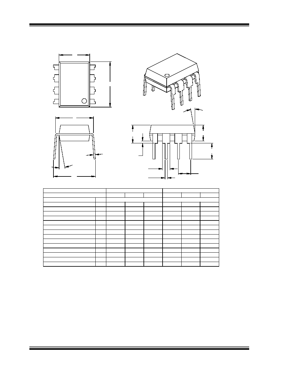
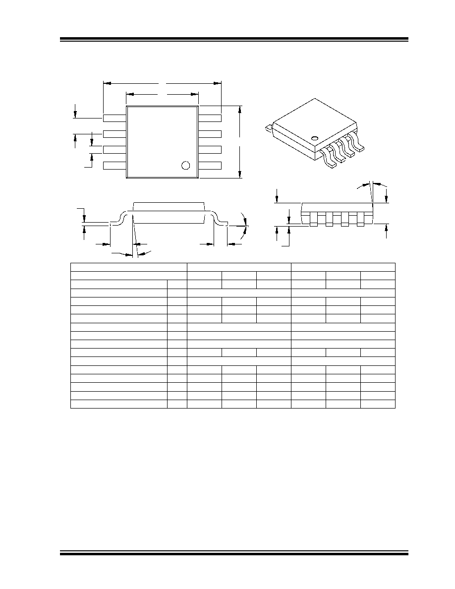
8-Lead Plastic Dual In-line (P) ≠ 300 mil (PDIP)
B1
B
A1
A
L
A2
p
E
eB
c
E1
n
D
1
2
Units
INCHES*
MILLIMETERS
Dimension Limits
MIN
NOM
MAX
MIN
NOM
MAX
Number of Pins
n
8
8
Pitch
p
.100
2.54
Top to Seating Plane
A
.140
.155
.170
3.56
3.94
4.32
Molded Package Thickness
A2
.115
.130
.145
2.92
3.30
3.68
Base to Seating Plane
A1
.015
0.38
Shoulder to Shoulder Width
E
.300
.313
.325
7.62
7.94
8.26
Molded Package Width
E1
.240
.250
.260
6.10
6.35
6.60
Overall Length
D
.360
.373
.385
9.14
9.46
9.78
Tip to Seating Plane
L
.125
.130
.135
3.18
3.30
3.43
Lead Thickness
c
.008
.012
.015
0.20
0.29
0.38
Upper Lead Width
B1
.045
.058
.070
1.14
1.46
1.78
Lower Lead Width
B
.014
.018
.022
0.36
0.46
0.56
Overall Row Spacing
ß
eB
.310
.370
.430
7.87
9.40
10.92
Mold Draft Angle Top
5
10
15
5
10
15
Mold Draft Angle Bottom
5
10
15
5
10
15
* Controlling Parameter
Notes:
Dimensions D and E1 do not include mold flash or protrusions. Mold flash or protrusions shall not exceed .010" (0.254mm) per side.
JEDEC Equivalent: MS-001
Drawing No. C04-018
ß Significant Characteristic

©
2006 Microchip Technology Inc.
Preliminary
DS21832C-page 17
25AA010A/25LC010A
8-Lead Plastic Small Outline (SN) ≠ Narrow, 150 mil (SOIC)
Foot Angle
0
4
8
0
4
8
15
12
0
15
12
0
Mold Draft Angle Bottom
15
12
0
15
12
0
Mold Draft Angle Top
0.51
0.42
0.33
.020
.017
.013
B
Lead Width
0.25
0.23
0.20
.010
.009
.008
c
Lead Thickness
0.76
0.62
0.48
.030
.025
.019
L
Foot Length
0.51
0.38
0.25
.020
.015
.010
h
Chamfer Distance
5.00
4.90
4.80
.197
.193
.189
D
Overall Length
3.99
3.91
3.71
.157
.154
.146
E1
Molded Package Width
6.20
6.02
5.79
.244
.237
.228
E
Overall Width
0.25
0.18
0.10
.010
.007
.004
A1
Standoff
ß
1.55
1.42
1.32
.061
.056
.052
A2
Molded Package Thickness
1.75
1.55
1.35
.069
.061
.053
A
Overall Height
1.27
.050
p
Pitch
8
8
n
Number of Pins
MAX
NOM
MIN
MAX
NOM
MIN
Dimension Limits
MILLIMETERS
INCHES*
Units
2
1
D
n
p
B
E
E1
h
L
c
45
∞
A2
A
A1
* Controlling Parameter
Notes:
Dimensions D and E1 do not include mold flash or protrusions. Mold flash or protrusions shall not exceed .010" (0.254mm) per side.
JEDEC Equivalent: MS-012
Drawing No. C04-057
ß Significant Characteristic

25AA010A/25LC010A
DS21832C-page 18
Preliminary
©
2006 Microchip Technology Inc.
8-Lead Plastic Thin Shrink Small Outline (ST) ≠ 4.4 mm (TSSOP)
A2
A
A1
L
c
1
2
D
n
p
B
E
E1
10∞
5∞
0∞
10∞
5∞
0∞
Mold Draft Angle Bottom
10∞
5∞
0∞
10∞
5∞
0∞
Mold Draft Angle Top
0.30
0.25
0.19
.012
.010
.007
B
Lead Width
0.20
0.15
0.09
.008
.006
.004
c
Lead Thickness
0.70
0.60
0.50
.028
.024
.020
L
Foot Length
3.10
3.00
2.90
.122
.118
.114
D
Molded Package Length
4.50
4.40
4.30
.177
.173
.169
E1
Molded Package Width
6.50
6.38
6.25
.256
.251
.246
E
Overall Width
0.15
0.10
0.05
.006
.004
.002
A1
Standoff
0.95
0.90
0.85
.037
.035
.033
A2
Molded Package Thickness
1.10
1.05
1.00
.043
.041
.039
A
Overall Height
0.65
.026
p
Pitch
8
8
n
Number of Pins
MAX
NOM
MIN
MAX
NOM
MIN
Dimension Limits
MILLIMETERS*
INCHES
Units
Foot Angle
0∞
4∞
8∞
0∞
4∞
8∞
Dimensions D and E1 do not include mold flash or protrusions. Mold flash or protrusions shall not exceed .005" (0.127mm) per side.
Notes:
JEDEC Equivalent: MO-153
Revised 07-21-05
* Controlling Parameter
Drawing No. C04-086
©
2006 Microchip Technology Inc.
Preliminary
DS21832C-page 19
25AA010A/25LC010A
8-Lead Plastic Micro Small Outline Package (MS) (MSOP)
D
A
A1
L
c
A2
E1
E
p
B
n
1
2
F
Dimensions D and E1 do not include mold flash or protrusions. Mold flash or protrusions shall not exceed .010" (0.254mm) per side.
.037 REF
F
Footprint (Reference)
Notes:
Revised 07-21-05
* Controlling Parameter
Mold Draft Angle Top
Mold Draft Angle Bottom
Foot Angle
Lead Width
Lead Thickness
c
B
.003
.009
.006
.012
Dimension Limits
Overall Height
Molded Package Thickness
Molded Package Width
Overall Length
Foot Length
Standoff
Overall Width
Number of Pins
Pitch
A
L
E1
D
A1
E
A2
.016
.024
.118 BSC
.118 BSC
.000
.030
.193 BSC
.033
MIN
p
n
Units
.026 BSC
NOM
8
INCHES
0.95 REF
-
-
.009
.016
0.08
0.22
0∞
0.23
0.40
8∞
MILLIMETERS*
0.65 BSC
0.85
3.00 BSC
3.00 BSC
0.60
4.90 BSC
.043
.031
.037
.006
0.40
0.00
0.75
MIN
MAX
NOM
1.10
0.80
0.15
0.95
MAX
8
-
-
-
15∞
5∞
-
15∞
5∞
-
JEDEC Equivalent: MO-187
0∞
-
8∞
5∞
5∞
-
-
15∞
15∞
-
-
-
-
BSC: Basic Dimension. Theoretically exact value shown without tolerances.
REF: Reference Dimension, usually without tolerance, for information purposes only.
See ASME Y14.5M
See ASME Y14.5M
Drawing No. C04-111
25AA010A/25LC010A
DS21832C-page 20
Preliminary
©
2006 Microchip Technology Inc.
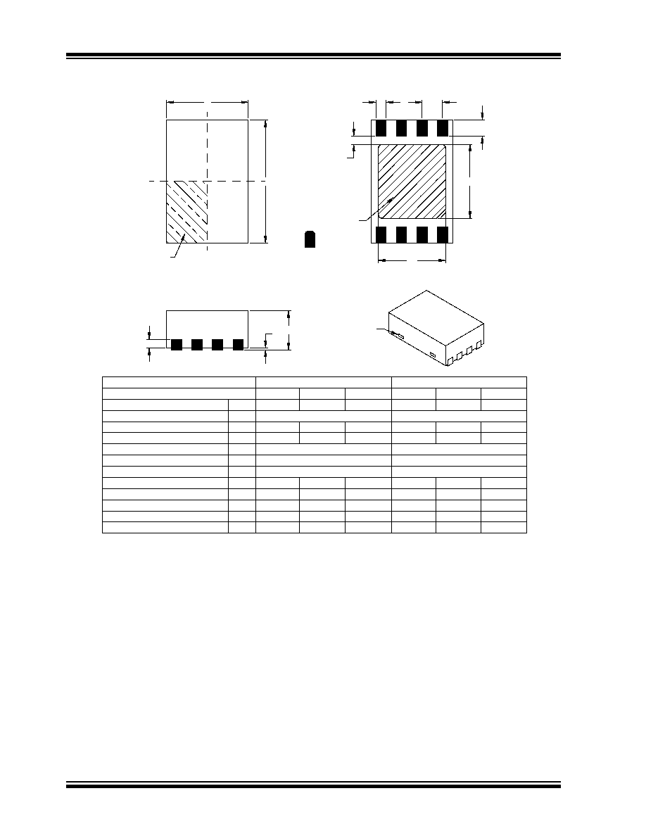
8-Lead Plastic Dual-Flat, No-Lead Package (MC) 2x3x0.9 mm Body (DFN) ≠ Saw Singulated
L
E2
A3
A1
A
TOP VIEW
D
E
EXPOSED
PAD
METAL
D2
BOTTOM VIEW
2
1
b
p
n
(NOTE 3)
EXPOSED
TIE BAR
PIN 1
(NOTE 1)
ID INDEX
AREA
(NOTE 2)
CONFIGURATION
CONTACT
ALTERNATE
DETAIL
K
3. Package may have one or more exposed tie bars at ends.
BSC: Basic Dimension. Theoretically exact value shown without tolerances.
REF: Reference Dimension, usually without tolerance, for information purposes only.
JEDEC Equivalent MO-229 VCED-2
See ASME Y14.5M
See ASME Y14.5M
MILLIMETERS*
0.50 BSC
2.00 BSC
0.20 REF.
3.00 BSC
1. Pin 1 visual index feature may vary, but must be located within the hatched area.
.039
.035
.031
0.80
A
Overall Height
2. Exposed pad may vary according to die attach paddle size.
* Controlling Parameter
Contact Length ß
Notes:
Contact Width
Standoff
Overall Width
Overall Length
Contact Thickness
Exposed Pad Width
Exposed Pad Length
.010
.008
L
b
.012
0.20
.001
.008 REF.
.079 BSC
≠
≠
.118 BSC
D
.051
.059
D2
E2
E
.000
A3
A1
.069
.075
1.30**
1.50**
.002
0.00
Dimension Limits
Pitch
Number of Pins
INCHES
.020 BSC
MIN
n
e
NOM
Units
8
MAX
MIN
1.00
0.90
0.25
0.30
≠
≠
1.75
1.90
0.02
0.05
8
NOM
MAX
Contact-to-Exposed Pad
ß
.012
K
.016
0.40
.020
0.30
0.50
** Not within JEDEC parameters
ß Significant Characteristic
.008
≠
≠
0.20
≠
≠
DWG No. C04-123
Revised 09-12-05

©
2006 Microchip Technology Inc.
Preliminary
DS21832C-page 21
25AA010A/25LC010A
6-Lead Plastic Small Outline Transistor (CH or OT) (SOT-23)
1
D
B
n
E
E1
L
c
A2
A
A1
p1
10
5
0
10
5
0
Mold Draft Angle Bottom
10
5
0
10
5
0
Mold Draft Angle Top
0.50
0.43
0.35
.020
.017
.014
B
Lead Width
0.20
0.15
0.09
.008
.006
.004
c
Lead Thickness
10
5
0
10
5
0
Foot Angle
0.55
0.45
0.35
.022
.018
.014
L
Foot Length
3.10
2.95
2.80
.122
.116
.110
D
Overall Length
1.75
1.63
1.50
.069
.064
.059
E1
Molded Package Width
3.00
2.80
2.60
.118
.110
.102
E
Overall Width
0.15
0.08
0.00
.006
.003
.000
A1
Standoff
1.30
1.10
0.90
.051
.043
.035
A2
Molded Package Thickness
1.45
1.18
0.90
.057
.046
.035
A
Overall Height
1.90 BSC
.075 BSC
p1
Outside lead pitch
0.95 BSC
.038 BSC
p
Pitch
6
6
n
Number of Pins
MAX
NOM
MIN
MAX
NOM
MIN
Dimension Limits
MILLIMETERS
INCHES*
Units
Dimensions D and E1 do not include mold flash or protrusions. Mold flash or protrusions shall not exceed .005" (0.127mm) per side.
Notes:
JEITA (formerly EIAJ) equivalent: SC-74A
* Controlling Parameter
Drawing No. C04-120
BSC: Basic Dimension. Theoretically exact value shown without tolerances.
See ASME Y14.5M
Revised 09-12-05

25AA010A/25LC010A
DS21832C-page 22
Preliminary
©
2006 Microchip Technology Inc.
APPENDIX A:
REVISION HISTORY
Revision B
Corrections to Section 1.0, Electrical Characteristics.
Revision C
Added Packages SOT-23, DFN and X-rotated TSSOP;
Revised AC Char., Params. 9, 10; Revised Package
Legend.

©
2006 Microchip Technology Inc.
Preliminary
DS21832C-page 21
25AA010A/25LC010A
THE MICROCHIP WEB SITE
Microchip provides online support via our WWW site at
www.microchip.com. This web site is used as a means
to make files and information easily available to
customers. Accessible by using your favorite Internet
browser, the web site contains the following
information:
∑ Product Support ≠ Data sheets and errata,
application notes and sample programs, design
resources, user's guides and hardware support
documents, latest software releases and archived
software
∑ General Technical Support ≠ Frequently Asked
Questions (FAQ), technical support requests,
online discussion groups, Microchip consultant
program member listing
∑ Business of Microchip ≠ Product selector and
ordering guides, latest Microchip press releases,
listing of seminars and events, listings of
Microchip sales offices, distributors and factory
representatives
CUSTOMER CHANGE NOTIFICATION
SERVICE
Microchip's customer notification service helps keep
customers current on Microchip products. Subscribers
will receive e-mail notification whenever there are
changes, updates, revisions or errata related to a
specified product family or development tool of interest.
To register, access the Microchip web site at
www.microchip.com, click on Customer Change
Notification and follow the registration instructions.
CUSTOMER SUPPORT
Users of Microchip products can receive assistance
through several channels:
∑ Distributor or Representative
∑ Local Sales Office
∑ Field Application Engineer (FAE)
∑ Technical Support
∑ Development Systems Information Line
Customers should contact their distributor,
representative or field application engineer (FAE) for
support. Local sales offices are also available to help
customers. A listing of sales offices and locations is
included in the back of this document.
Technical support is available through the web site
at: http://support.microchip.com

25AA010A/25LC010A
DS21832C-page 22
Preliminary
©
2006 Microchip Technology Inc.
READER RESPONSE
It is our intention to provide you with the best documentation possible to ensure successful use of your Microchip prod-
uct. If you wish to provide your comments on organization, clarity, subject matter, and ways in which our documentation
can better serve you, please FAX your comments to the Technical Publications Manager at (480) 792-4150.
Please list the following information, and use this outline to provide us with your comments about this document.
To:
Technical Publications Manager
RE:
Reader Response
Total Pages Sent ________
From: Name
Company
Address
City / State / ZIP / Country
Telephone: (_______) _________ - _________
Application (optional):
Would you like a reply? Y N
Device: Literature
Number:
Questions:
FAX: (______) _________ - _________
DS21832C
25AA010A/25LC010A
1.
What are the best features of this document?
2.
How does this document meet your hardware and software development needs?
3.
Do you find the organization of this document easy to follow? If not, why?
4.
What additions to the document do you think would enhance the structure and subject?
5.
What deletions from the document could be made without affecting the overall usefulness?
6.
Is there any incorrect or misleading information (what and where)?
7.
How would you improve this document?

©
2006 Microchip Technology Inc.
Preliminary
DS21832C-page 23
25AA010A/25LC010A
PRODUCT IDENTIFICATION SYSTEM
To order or obtain information, e.g., on pricing or delivery, refer to the factory or the listed sales office
.
Sales and Support
PART NO.
X
/XX
Package
Tape & Reel
Device
Device:
25AA010A
25LC010A
1k-Bit, 1.8V, 16 Byte Page, SPI Serial EEPROM
1k-Bit, 2.5V, 16 Byte Page, SPI Serial EEPROM
Tape & Reel:
Blank =
T
=
Standard packaging
Tape & Reel
Temperature
Range:
I
=
E
=
-40
∞
C to+85
∞
C
-40
∞
C to+125
∞
C
Package:
MS
=
P
=
SN
=
ST
=
MC
=
OT
=
Plastic MSOP (Micro Small Outline), 8-lead
Plastic DIP (300 mil body), 8-lead
Plastic SOIC (150 mil body), 8-lead
TSSOP, 8-lead
2x3 DFN, 8-lead
SOT-23, 6-lead (Tape and Reel only)
Examples:
a)
25AA010A-I/MS = 1k-bit, 16-byte page, 1.8V
Serial EEPROM, Industrial temp., MSOP
package
b)
25AA010AT-I/SN = 1k-bit, 16-byte page, 1.8V
Serial EEPROM, Industrial temp., Tape & Reel,
SOIC package
c)
25LC010AT-I/SN = 1k-bit, 16-byte page, 2.5V
Serial EEPROM, Industrial temp., Tape & Reel,
SOIC package
d)
25LC010AT-I/ST = 1k-bit, 16-byte page, 2.5V
Serial EEPROM, Industrial temp., Tape & Reel,
TSSOP package
e)
25LC010AT-E/SN = 1k-bit, 16-byte page, 2.5V
serial EEPROM, Extended temp., Tape & Reel,
SOIC Package
≠
X
Temperature
Data Sheets
Products supported by a preliminary Data Sheet may have an errata sheet describing minor operational differences and
recommended workarounds. To determine if an errata sheet exists for a particular device, please contact one of the following:
1.
Your local Microchip sales office
2.
The Microchip Corporate Literature Center U.S. FAX: (480) 792-7277
3.
The Microchip Worldwide Site (www.microchip.com)
Please specify which device, revision of silicon and Data Sheet (include Literature #) you are using.
New Customer Notification System
Register on our web site (www.microchip.com/cn) to receive the most current information on our products.

25AA010A/25LC010A
DS21832C-page 24
Preliminary
©
2006 Microchip Technology Inc.
NOTES:
©
2006 Microchip Technology Inc.
Preliminary
DS21832C-page 25
Information contained in this publication regarding device
applications and the like is provided only for your convenience
and may be superseded by updates. It is your responsibility to
ensure that your application meets with your specifications.
MICROCHIP MAKES NO REPRESENTATIONS OR WAR-
RANTIES OF ANY KIND WHETHER EXPRESS OR IMPLIED,
WRITTEN OR ORAL, STATUTORY OR OTHERWISE,
RELATED TO THE INFORMATION, INCLUDING BUT NOT
LIMITED TO ITS CONDITION, QUALITY, PERFORMANCE,
MERCHANTABILITY OR FITNESS FOR PURPOSE.
Microchip disclaims all liability arising from this information and
its use. Use of Microchip devices in life support and/or safety
applications is entirely at the buyer's risk, and the buyer agrees
to defend, indemnify and hold harmless Microchip from any and
all damages, claims, suits, or expenses resulting from such
use. No licenses are conveyed, implicitly or otherwise, under
any Microchip intellectual property rights.
Trademarks
The Microchip name and logo, the Microchip logo, Accuron,
dsPIC, K
EE
L
OQ
, micro
ID
, MPLAB, PIC, PICmicro, PICSTART,
PRO MATE, PowerSmart, rfPIC, and SmartShunt are
registered trademarks of Microchip Technology Incorporated
in the U.S.A. and other countries.
AmpLab, FilterLab, Migratable Memory, MXDEV, MXLAB,
SEEVAL, SmartSensor and The Embedded Control Solutions
Company are registered trademarks of Microchip Technology
Incorporated in the U.S.A.
Analog-for-the-Digital Age, Application Maestro, dsPICDEM,
dsPICDEM.net, dsPICworks, ECAN, ECONOMONITOR,
FanSense, FlexROM, fuzzyLAB, In-Circuit Serial
Programming, ICSP, ICEPIC, Linear Active Thermistor,
MPASM, MPLIB, MPLINK, MPSIM, PICkit, PICDEM,
PICDEM.net, PICLAB, PICtail, PowerCal, PowerInfo,
PowerMate, PowerTool, Real ICE, rfLAB, rfPICDEM, Select
Mode, Smart Serial, SmartTel, Total Endurance, UNI/O,
WiperLock and Zena are trademarks of Microchip Technology
Incorporated in the U.S.A. and other countries.
SQTP is a service mark of Microchip Technology Incorporated
in the U.S.A.
All other trademarks mentioned herein are property of their
respective companies.
© 2006, Microchip Technology Incorporated, Printed in the
U.S.A., All Rights Reserved.
Printed on recycled paper.
Note the following details of the code protection feature on Microchip devices:
∑
Microchip products meet the specification contained in their particular Microchip Data Sheet.
∑
Microchip believes that its family of products is one of the most secure families of its kind on the market today, when used in the
intended manner and under normal conditions.
∑
There are dishonest and possibly illegal methods used to breach the code protection feature. All of these methods, to our
knowledge, require using the Microchip products in a manner outside the operating specifications contained in Microchip's Data
Sheets. Most likely, the person doing so is engaged in theft of intellectual property.
∑
Microchip is willing to work with the customer who is concerned about the integrity of their code.
∑
Neither Microchip nor any other semiconductor manufacturer can guarantee the security of their code. Code protection does not
mean that we are guaranteeing the product as "unbreakable."
Code protection is constantly evolving. We at Microchip are committed to continuously improving the code protection features of our
products. Attempts to break Microchip's code protection feature may be a violation of the Digital Millennium Copyright Act. If such acts
allow unauthorized access to your software or other copyrighted work, you may have a right to sue for relief under that Act.
Microchip received ISO/TS-16949:2002 quality system certification for
its worldwide headquarters, design and wafer fabrication facilities in
Chandler and Tempe, Arizona and Mountain View, California in
October 2003. The Company's quality system processes and
procedures are for its PICmicro
Æ
8-bit MCUs, K
EE
L
OQ
Æ
code hopping
devices, Serial EEPROMs, microperipherals, nonvolatile memory and
analog products. In addition, Microchip's quality system for the design
and manufacture of development systems is ISO 9001:2000 certified.

DS21832C-page 26
Preliminary
©
2006 Microchip Technology Inc.
AMERICAS
Corporate Office
2355 West Chandler Blvd.
Chandler, AZ 85224-6199
Tel: 480-792-7200
Fax: 480-792-7277
Technical Support:
http://support.microchip.com
Web Address:
www.microchip.com
Atlanta
Alpharetta, GA
Tel: 770-640-0034
Fax: 770-640-0307
Boston
Westborough, MA
Tel: 774-760-0087
Fax: 774-760-0088
Chicago
Itasca, IL
Tel: 630-285-0071
Fax: 630-285-0075
Dallas
Addison, TX
Tel: 972-818-7423
Fax: 972-818-2924
Detroit
Farmington Hills, MI
Tel: 248-538-2250
Fax: 248-538-2260
Kokomo
Kokomo, IN
Tel: 765-864-8360
Fax: 765-864-8387
Los Angeles
Mission Viejo, CA
Tel: 949-462-9523
Fax: 949-462-9608
San Jose
Mountain View, CA
Tel: 650-215-1444
Fax: 650-961-0286
Toronto
Mississauga, Ontario,
Canada
Tel: 905-673-0699
Fax: 905-673-6509
ASIA/PACIFIC
Australia - Sydney
Tel: 61-2-9868-6733
Fax: 61-2-9868-6755
China - Beijing
Tel: 86-10-8528-2100
Fax: 86-10-8528-2104
China - Chengdu
Tel: 86-28-8676-6200
Fax: 86-28-8676-6599
China - Fuzhou
Tel: 86-591-8750-3506
Fax: 86-591-8750-3521
China - Hong Kong SAR
Tel: 852-2401-1200
Fax: 852-2401-3431
China - Qingdao
Tel: 86-532-8502-7355
Fax: 86-532-8502-7205
China - Shanghai
Tel: 86-21-5407-5533
Fax: 86-21-5407-5066
China - Shenyang
Tel: 86-24-2334-2829
Fax: 86-24-2334-2393
China - Shenzhen
Tel: 86-755-8203-2660
Fax: 86-755-8203-1760
China - Shunde
Tel: 86-757-2839-5507
Fax: 86-757-2839-5571
China - Wuhan
Tel: 86-27-5980-5300
Fax: 86-27-5980-5118
China - Xian
Tel: 86-29-8833-7250
Fax: 86-29-8833-7256
ASIA/PACIFIC
India - Bangalore
Tel: 91-80-2229-0061
Fax: 91-80-2229-0062
India - New Delhi
Tel: 91-11-5160-8631
Fax: 91-11-5160-8632
India - Pune
Tel: 91-20-2566-1512
Fax: 91-20-2566-1513
Japan - Yokohama
Tel: 81-45-471- 6166
Fax: 81-45-471-6122
Korea - Gumi
Tel: 82-54-473-4301
Fax: 82-54-473-4302
Korea - Seoul
Tel: 82-2-554-7200
Fax: 82-2-558-5932 or
82-2-558-5934
Malaysia - Penang
Tel: 60-4-646-8870
Fax: 60-4-646-5086
Philippines - Manila
Tel: 63-2-634-9065
Fax: 63-2-634-9069
Singapore
Tel: 65-6334-8870
Fax: 65-6334-8850
Taiwan - Hsin Chu
Tel: 886-3-572-9526
Fax: 886-3-572-6459
Taiwan - Kaohsiung
Tel: 886-7-536-4818
Fax: 886-7-536-4803
Taiwan - Taipei
Tel: 886-2-2500-6610
Fax: 886-2-2508-0102
Thailand - Bangkok
Tel: 66-2-694-1351
Fax: 66-2-694-1350
EUROPE
Austria - Wels
Tel: 43-7242-2244-399
Fax: 43-7242-2244-393
Denmark - Copenhagen
Tel: 45-4450-2828
Fax: 45-4485-2829
France - Paris
Tel: 33-1-69-53-63-20
Fax: 33-1-69-30-90-79
Germany - Munich
Tel: 49-89-627-144-0
Fax: 49-89-627-144-44
Italy - Milan
Tel: 39-0331-742611
Fax: 39-0331-466781
Netherlands - Drunen
Tel: 31-416-690399
Fax: 31-416-690340
Spain - Madrid
Tel: 34-91-708-08-90
Fax: 34-91-708-08-91
UK - Wokingham
Tel: 44-118-921-5869
Fax: 44-118-921-5820
W
ORLDWIDE
S
ALES
AND
S
ERVICE
10/31/05