
©
2006 Microchip Technology Inc.
Advance Information
DS70178A
dsPIC30F1010/202X
Data Sheet
28/44-Pin High-Performance
Switch Mode Power Supply
Digital Signal Controllers

DS70178A-page ii
Advance Information
©
2006 Microchip Technology Inc.
Information contained in this publication regarding device
applications and the like is provided only for your convenience
and may be superseded by updates. It is your responsibility to
ensure that your application meets with your specifications.
MICROCHIP MAKES NO REPRESENTATIONS OR
WARRANTIES OF ANY KIND WHETHER EXPRESS OR
IMPLIED, WRITTEN OR ORAL, STATUTORY OR
OTHERWISE, RELATED TO THE INFORMATION,
INCLUDING BUT NOT LIMITED TO ITS CONDITION,
QUALITY, PERFORMANCE, MERCHANTABILITY OR
FITNESS FOR PURPOSE. Microchip disclaims all liability
arising from this information and its use. Use of Microchip
devices in life support and/or safety applications is entirely at
the buyer's risk, and the buyer agrees to defend, indemnify and
hold harmless Microchip from any and all damages, claims,
suits, or expenses resulting from such use. No licenses are
conveyed, implicitly or otherwise, under any Microchip
intellectual property rights.
Trademarks
The Microchip name and logo, the Microchip logo, Accuron,
dsPIC, K
EE
L
OQ
, micro
ID
, MPLAB, PIC, PICmicro, PICSTART,
PRO MATE, PowerSmart, rfPIC and SmartShunt are
registered trademarks of Microchip Technology Incorporated
in the U.S.A. and other countries.
AmpLab, FilterLab, Migratable Memory, MXDEV, MXLAB,
SEEVAL, SmartSensor and The Embedded Control Solutions
Company are registered trademarks of Microchip Technology
Incorporated in the U.S.A.
Analog-for-the-Digital Age, Application Maestro, dsPICDEM,
dsPICDEM.net, dsPICworks, ECAN, ECONOMONITOR,
FanSense, FlexROM, fuzzyLAB, In-Circuit Serial
Programming, ICSP, ICEPIC, Linear Active Thermistor, Mindi,
MiWi, MPASM, MPLIB, MPLINK, PICkit, PICDEM,
PICDEM.net, PICLAB, PICtail, PowerCal, PowerInfo,
PowerMate, PowerTool, REAL ICE, rfLAB, rfPICDEM, Select
Mode, Smart Serial, SmartTel, Total Endurance, UNI/O,
WiperLock and ZENA are trademarks of Microchip
Technology Incorporated in the U.S.A. and other countries.
SQTP is a service mark of Microchip Technology Incorporated
in the U.S.A.
All other trademarks mentioned herein are property of their
respective companies.
© 2006, Microchip Technology Incorporated, Printed in the
U.S.A., All Rights Reserved.
Printed on recycled paper.
Note the following details of the code protection feature on Microchip devices:
∑
Microchip products meet the specification contained in their particular Microchip Data Sheet.
∑
Microchip believes that its family of products is one of the most secure families of its kind on the market today, when used in the
intended manner and under normal conditions.
∑
There are dishonest and possibly illegal methods used to breach the code protection feature. All of these methods, to our
knowledge, require using the Microchip products in a manner outside the operating specifications contained in Microchip's Data
Sheets. Most likely, the person doing so is engaged in theft of intellectual property.
∑
Microchip is willing to work with the customer who is concerned about the integrity of their code.
∑
Neither Microchip nor any other semiconductor manufacturer can guarantee the security of their code. Code protection does not
mean that we are guaranteeing the product as "unbreakable."
Code protection is constantly evolving. We at Microchip are committed to continuously improving the code protection features of our
products. Attempts to break Microchip's code protection feature may be a violation of the Digital Millennium Copyright Act. If such acts
allow unauthorized access to your software or other copyrighted work, you may have a right to sue for relief under that Act.
Microchip received ISO/TS-16949:2002 certification for its worldwide
headquarters, design and wafer fabrication facilities in Chandler and
Tempe, Arizona, Gresham, Oregon and Mountain View, California. The
Company's quality system processes and procedures are for its
PICmicro
Æ
8-bit MCUs, K
EE
L
OQ
Æ
code hopping devices, Serial
EEPROMs, microperipherals, nonvolatile memory and analog
products. In addition, Microchip's quality system for the design and
manufacture of development systems is ISO 9001:2000 certified.

©
2006 Microchip Technology Inc.
Advance Information
DS70178A-page 1
dsPIC30F1010/202X
High-Performance Modified RISC CPU:
∑ Modified Harvard architecture
∑ C compiler optimized instruction set architecture
∑ 83 base instructions with flexible addressing
modes
∑ 24-bit wide instructions, 16-bit wide data path
∑ 12 Kbytes on-chip Flash program space
∑ 512 bytes on-chip data RAM
∑ 16 x 16-bit working register array
∑ Up to 30 MIPs operation:
- Dual Internal RC 9.7 and 14.55 MHz (±1%)
- 32X PLL with 480 MHz VCO
- PLL inputs ±3%
- External EC clock 9.7 and 14.55 MHz
- HS Crystal mode 9.7 and 14.55 MHz
∑ 32 interrupt sources
∑ Three external interrupt sources
∑ 8 user-selectable priority levels for each interrupt
∑ 4 processor exceptions and software traps
DSP Engine Features:
∑ Modulo and Bit-Reversed modes
∑ Two 40-bit wide accumulators with optional
saturation logic
∑ 17-bit x 17-bit single-cycle hardware fractional/
integer multiplier
∑ Single-cycle Multiply-Accumulate (MAC)
operation
∑ 40-stage Barrel Shifter
∑ Dual data fetch
Peripheral Features:
∑ High-current sink/source I/O pins: 25 mA/25 mA
∑ Three 16-bit timers/counters; optionally pair up
16-bit timers into 32-bit timer modules
∑ Four 16-bit Capture input functions
∑ Two 16-bit Compare/PWM output functions
- Dual Compare mode available
∑ 3-wire SPI modules (supports 4 Frame modes)
∑ I
2
C
TM
module supports Multi-Master/Slave mode
and 7-bit/10-bit addressing
∑ UART Module:
- Supports RS-232, RS-485 and LIN 1.2
- Supports IrDA
Æ
with on-chip hardware endec
- Auto wake-up on Start bit
- Auto-Baud Detect
- 4-level FIFO buffer
SMPS PWM Module Features:
∑ Four PWM generators with 8 outputs
∑ Each PWM generator has independent time base
and duty cycle
∑ Duty cycle resolution of 1.1 ns at 30 MIPS
∑ Individual dead time for each PWM generator:
- Dead-time resolution 4.2 ns at 30 MIPS
- Dead time for rising and falling edges
∑ Phase-shift resolution of 4.2 ns @ 30 MIPS
∑ Frequency resolution of 8.4 ns @ 30 MIPS
∑ PWM modes supported:
- Complementary
- Push-Pull
- Multi-Phase
- Variable Phase
- Current Reset
- Current-Limit
∑ Independent Current-Limit and Fault Inputs
∑ Output Override Control
∑ Special Event Trigger
∑ PWM generated ADC Trigger
Note: This data sheet summarizes features of this group
of dsPIC30F devices and is not intended to be a complete
reference source. For more information on the CPU,
peripherals, register descriptions and general device
functionality, refer to the "dsPIC30F Family Reference
Manual" (DS70046). For more information on the device
instruction set and programming, refer to the "dsPIC30F/
33F Programmer's Reference Manual" (DS70157).
28/44-pin dsPIC30F1010/202X Enhanced Flash
SMPS 16-bit Digital Signal Controller

dsPIC30F1010/202X
DS70178A-page 2
Advance Information
©
2006 Microchip Technology Inc.
Analog Features:
ADC
∑ 10-bit resolution
∑ 2000 Ksps conversion rate
∑ Up to 12 input channels
∑ "Conversion pairing" allows simultaneous conver-
sion of two inputs (i.e., current and voltage) with a
single trigger
∑ PWM control loop:
- Up to six conversion pairs available
- Each conversion pair has up to four PWM
and seven other selectable trigger sources
∑ Interrupt hardware supports up to 1M interrupts
per second
COMPARATOR
∑ Four Analog Comparators:
- 20 ns response time
- 10-bit DAC reference generator
- Programmable output polarity
- Selectable input source
- ADC sample and convert capable
∑ PWM module interface
- PWM Duty Cycle Control
- PWM Period Control
- PWM Fault Detect
∑ Special Event Trigger
∑ PWM-generated ADC Trigger
Special Microcontroller Features:
∑ Enhanced Flash program memory:
- 10,000 erase/write cycle (min.) for
industrial temperature range, 100k (typical)
∑ Self-reprogrammable under software control
∑ Power-on Reset (POR), Power-up Timer (PWRT)
and Oscillator Start-up Timer (OST)
∑ Flexible Watchdog Timer (WDT) with on-chip low
power RC oscillator for reliable operation
∑ Fail-Safe clock monitor operation
∑ Detects clock failure and switches to on-chip low
power RC oscillator
∑ Programmable code protection
∑ In-Circuit Serial ProgrammingTM (ICSPTM)
∑ Selectable Power Management modes
- Sleep, Idle and Alternate Clock modes
CMOS Technology:
∑ Low-power, high-speed Flash technology
∑ 3.0V and 5.0V operation (±10%)
∑ Industrial and Extended temperature ranges
∑ Low power consumption
dsPIC30F SWITCH MODE POWER SUPPLY FAMILY:
Product
Pins
Pac
kag
ing
Program
Me
mo
ry
(B
ytes
)
Da
t
a
SRAM
(B
ytes
)
Tim
e
r
s
Ca
p
t
ure
Com
p
a
r
e
UAR
T
SPI
I
2
CTM
PW
M
AD
Cs
S & H
A/D
Inp
u
t
s
Ana
l
o
g
C
o
mp
ar
ator
s
dsPIC30F1010
28
SDIP
6K
256
2
0
1
1
1
1
2x2
1
2
6 ch
2
dsPIC30F1010
28
SOIC
6K
256
2
0
1
1
1
1
2x2
1
2
6 ch
2
dsPIC30F1010
28
QFN
6K
256
2
0
1
1
1
1
2x2
1
2
6 ch
2
dsPIC30F2020
28
SDIP
12K
512
3
1
2
1
1
1
4x2
1
4
8 ch
4
dsPIC30F2020
28
SOIC
12K
512
3
1
2
1
1
1
4x2
1
4
8 ch
4
dsPIC30F2020
28
QFN
12K
512
3
1
2
1
1
1
4x2
1
4
8 ch
4
dsPIC30F2023
44
QFN
12K
512
3
1
2
1
1
1
4x2
1
4
12 ch
4
dsPIC30F2023
44
TQFP
12K
512
3
1
2
1
1
1
4x2
1
4
12 ch
4
©
2006 Microchip Technology Inc.
Advance Information
DS70178A-page 3
dsPIC30F1010/202X
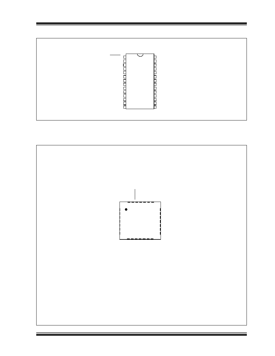
Pin Diagrams
28-Pin SDIP and SOIC
d
s
P
I
C
3
0F1
010
MCLR
PWM1L/RE0
PWM1H/RE1
PWM2L/RE2
PWM2H/RE3
RE4
RE5
V
SS
V
DD
AN0/CMP1A/CN2/RB0
AN1/CMP1B/CN3/RB1
AV
DD
AV
SS
AN2/CMP1C/CMP2A/CN4/RB2
PGC2/EMUD2/SCK1/SFLT3/INT2/RF6
PGD2/EMUC2/OC1/SFLT1/INT1/RD0
EMUC1/EXTREF/T1CK/U1ARX/CN0/RE6
EMUD1/PGD1/U1ATX/CN1/T2CK/RE7
V
SS
OSC2/CLKO/RB7
OSC1/CLKI/RB6
V
DD
SFLT2/INT0/OCFLTA/RA9
PGC/EMUC/SDI1/SDA/U1RX/RF7
PGD/EMUD/SDO1/SCL/U1TX/RF8
AN5/CMP2D/CN7/RB5
AN4/CMP2C/CN6/RB4
AN3/CMP1D/CMP2B/CN5/RB3
1
2
3
4
5
6
7
8
9
10
11
12
13
14
28
27
26
25
24
23
22
21
20
19
18
17
16
15
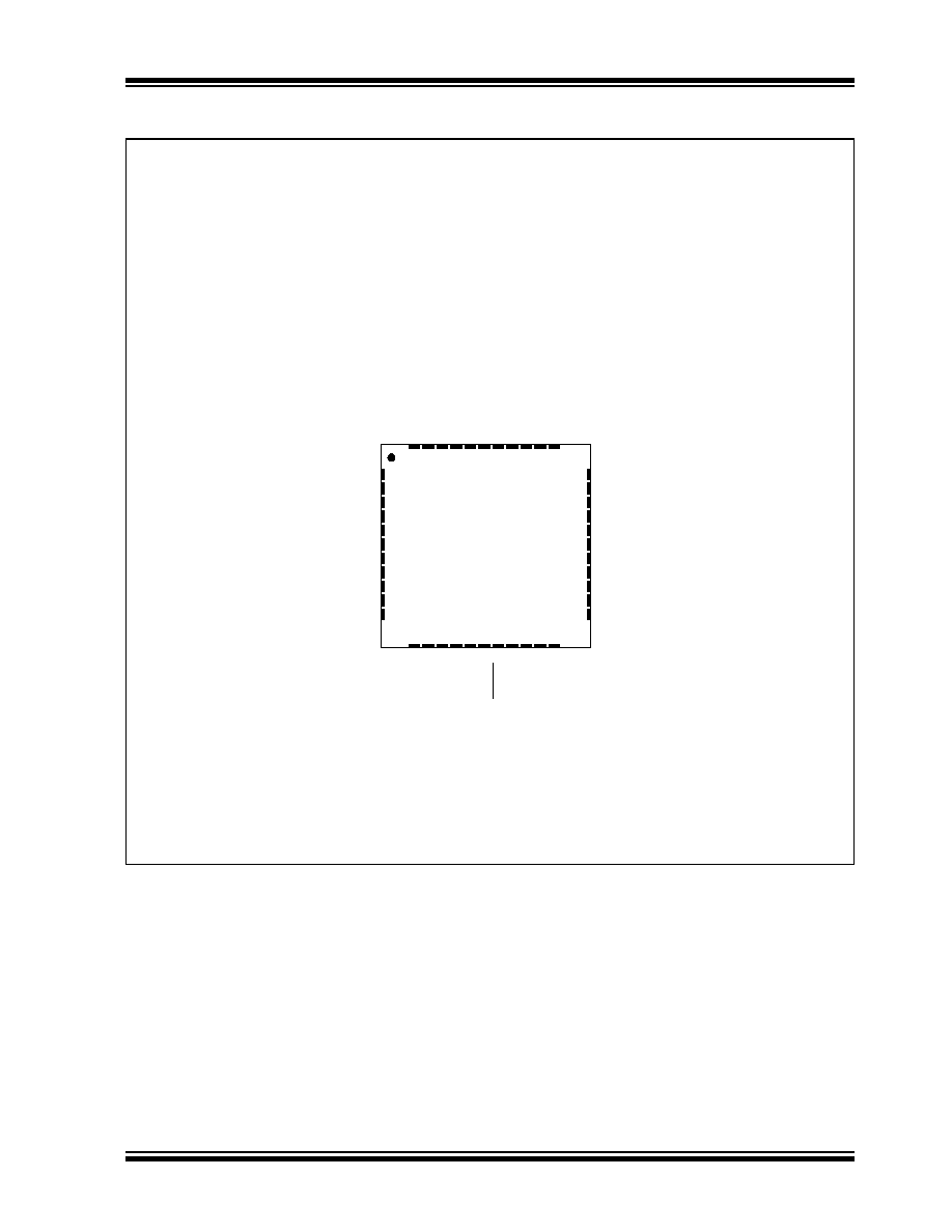
28-Pin QFN
10 11
2
3
6
1
18
19
20
21
22
12 13 14
15
8
7
16
17
23
24
25
26
27
28
9
dsPIC30F1010
PG
D1
/
E
MUD
1
/
T
2
C
K/
U
1
A
T
X/
C
N
1
/
RE7
5
4
AV
DD
AV
SS
PWM1
L
/
RE0
PWM1
H/
R
E
1
PWM2L/RE2
PWM2H/RE3
RE4
RE5
V
DD
V
SS
PGC/EMUC/SDI1/SDA/U1RX/RF7
P
G
D
/
EM
UD
/SDO
1/
SCL
/
U1
T
X
/RF
8
S
F
LT2
/
IN
T0
/
O
CF
LTA
/
R
A
9
P
G
C
2
/E
M
UC2
/O
C1
/S
F
L
T
1
/IC1
/INT
1
/RD
0
MC
LR
AN0
/
C
M
P1
A/
C
N
2
/
RB0
AN1
/
C
M
P1
B/
C
N
3
/
RB1
AN2/CMP1C/CMP2A/CN4/RB2
AN3/CMP1D/CMP2B/CN5/RB3
AN4/CMP2C/CN6/RB4
AN5/CMP2D/CN7/RB5
V
SS
OSC1/CLKI/RB6
OSC2/CLKO/RB7
PG
C
1
/
E
MU
C1
/
EXTREF/
U
1
AR
X/
T1
C
K
/
C
N
0
/
R
E6
V
DD
P
G
D2
/E
M
U
D
2
/S
C
K
1
/
S
F
LT
3/
INT
2
/
R
F
6

dsPIC30F1010/202X
DS70178A-page 4
Advance Information
©
2006 Microchip Technology Inc.
28-Pin SDIP and SOIC
dsP
I
C
3
0F
202
0
MCLR
PWM1L/RE0
PWM1H/RE1
PWM2L/RE2
PWM2H/RE3
PWM3L/RE4
PWM3H/RE5
V
SS
V
DD
AN0/CMP1A/CN2/RB0
AN1/CMP1B/CN3/RB1
AV
DD
AV
SS
AN2/CMP1C/CMP2A/CN4/RB2
PGD2/EMUD2/SCK1/SFLT3/OC2/INT2/RF6
PGC2/EMUC2/OC1/SFLT1/IC1/INT1/RD0
EMUC1/PGC1/EXTREF/PWM4L/U1ARX/CN0/T1CK/RE6
PGD1/EMUD1/PWM4H/U1ATX/CN1/T2CK/RE7
V
SS
AN7/CMP3D/CMP4B/OSC2/CLKO/RB7
AN6/CMP3C/CMP4A/OSC1/CLKI/RB6
V
DD
SFLT2/INT0/OCFLTA/RA9
PGC/EMUC/SDI1/SDA/U1RX/RF7
PGD/EMUD/SDO1/SCL/U1TX/RF8
AN5/CMP2D/CMP3B/CN7/RB5
AN4/CMP2C/CMP3A/CN6/RB4
AN3/CMP1D/CMP2B/CN5/RB3
1
2
3
4
5
6
7
8
9
10
11
12
13
14
28
27
26
25
24
23
22
21
20
19
18
17
16
15
28-Pin QFN
10 11
2
3
6
1
18
19
20
21
22
12 13 14
15
8
7
16
17
23
24
25
26
27
28
9
dsPIC30F2020
PGD
1
/E
M
UD1
/PW
M
4H
/T
2CK
/
U1
A
T
X
/
CN
1/R
E
7
5
4
AV
DD
AV
SS
PW
M1
L
/
RE0
PW
M
1
H/
RE1
PWM2L/RE2
PWM2H/RE3
PWM3L/RE4
PWM3H/RE5
V
DD
V
SS
PGC/EMUC/SDI1/SDA/U1RX/RF7
PG
D
/
EMUD
/
S
DO
1
/
SCL
/
U1
TX/
R
F8
S
F
LT
2
/INT
0
/OC
F
LT
A
/
R
A
9
P
G
C2/
E
M
U
C
2
/O
C1
/S
F
L
T
1
/IC1
/IN
T
1
/RD
0
MC
LR
AN
0
/
C
M
P1
A/
CN2
/
R
B
0
AN
1
/
C
M
P1
B/
CN3
/
R
B
1
AN2/CMP1C/CMP2A/CN4/RB2
AN3/CMP1D/CMP2B/CN5/RB3
AN4/CMP2C/CMP3A/CN6/RB4
AN5/CMP2D/CMP3B/CN7/RB5
V
SS
AN6/CMP3C/CMP4A/OSC1/CLKI/RB6
AN7/CMP3D/CMP4B/OSC2/CLKO/RB7
PG
C
1
/EM
U
C1
/EXT
REF
/
PW
M
4
L
/
T
1
C
K
/U1
A
RX
/CN0
/R
E6
V
DD
P
G
D
2
/E
M
U
D2
/S
CK
1
/
S
F
L
T
3
/
O
C
2
/INT
2
/RF
6
©
2006 Microchip Technology Inc.
Advance Information
DS70178A-page 5
dsPIC30F1010/202X
Pin Diagrams
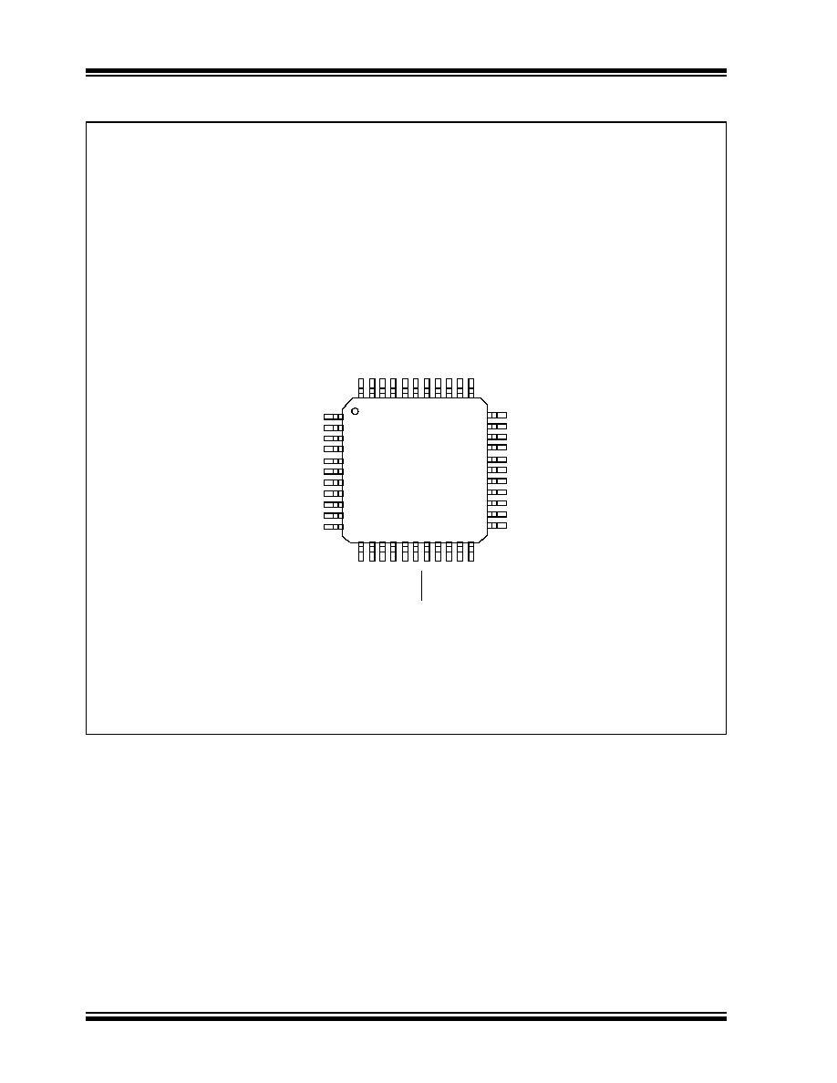
44-PIN QFN
44
dsPIC30F2023
43 42 41 40 39 38 37 36 35
12 13 14 15 16 17 18 19 20 21
3
30
29
28
27
26
25
24
23
4
5
7
8
9
10
11
1
2
32
31
6
22
33
34
AN4/CMP2C/CMP3A/CN6/RB4
AN5/CMP2D/CMP3B/CN7/RB5
AN6/CMP3C/CMP4A/OSC1/CLKI/RB6
AN7/CMP3D/CMP4B/OSC2/CLKO/RB7
AN8/CMP4C/RB8
AN10/IFLT4/RB10
V
DD
AN11/IFLT2/RB11
V
SS
P
G
D
/
EM
UD
/SDO
1/
RF
8
AN
9
/
EX
T
R
EF/
C
MP4
D
/
R
B9
P
G
C
2
/E
M
U
C2
/OC
1
/
I
C1
/INT
1
/RD
0
V
DD
PG
C1
/
E
MUC
1
/
P
WM4
L
/
T
1
C
K/
U
1
AR
X/
CN
0
/
R
E
6
OC
2/
R
D
1
V
SS
S
F
L
T
2
/INT
0
/O
CF
L
T
A
/
R
A
9
P
G
D
2
/E
M
U
D2
/S
CK
1
/IN
T
2
/RF
6
SFL
T
1
/
RA8
PG
D1
/EM
U
D1
/
PWM
4
H/T
2
CK/U
1A
T
X
/C
N1
/RE7
PWM2H/RE3
PWM3L/RE4
PWM3H/RE5
V
DD
V
SS
SYNCO/SSI/RF15
SDA/RG3
SFLT4/RA11
SFLT3/RA10
PGC/EMUC/SDI1/RF7
PWM2L/RE2
AN3/CMP1D/CMP2B/CN5/RB3
AN2/CMP1C/CMP2A/CN4/RB2
EMUC
3
/
AN
1
/
CMP1
B/
CN
3
/
R
B
1
EMUD
3
/
AN
0
/
C
M
P1
A/
CN2
/
R
B
0
MC
LR
U1
RX
/
R
F
2
AV
DD
AV
SS
PW
M
1
L
/
RE
0
PWM
1
H/RE1
SYNC
I
/
R
F1
4
U1
T
X
/RF
3
S
C
L/
R
G
2
dsPIC30F1010/202X
DS70178A-page 6
Advance Information
©
2006 Microchip Technology Inc.
Pin Diagrams
10
11
2
3
4
5
6
1
18
19
20
21
22
12
13
14
15
38
8
7
44
43
42
41
40
39
16
17
29
30
31
32
33
23
24
25
26
27
28
36
34
35
9
37
PG
D/E
M
UD/S
D
O
1
/R
F
8
AN9
/
EXTREF/
C
M
P4
D
/
RB9
P
G
C2
/E
M
U
C2/
O
C
1
/IC
1/I
N
T
1
/R
D0
V
DD
PG
C1
/
E
MUC
1
/
P
WM4
L
/
T
1
C
K/
U
1
AR
X/
CN
0
/
R
E
6
SYN
CI
/
R
F1
4
V
SS
S
F
L
T
2
/IN
T
0
/RA
9
P
G
D2
/E
M
U
D2/
S
CK
1
/INT
2
/RF
6
SFL
T
1
/
RA
8
AN3/CMP1D/CMP2B/CN5/RB3
AN2/CMP1C/CMP2A/CN4/RB2
AN
1
/
EMU
C
3
/
CMP1
B/
CN
3
/
R
B
1
AN
0
/
EMU
D
3
/
CMP1
A/
CN
2
/
R
B
0
MCL
R
U1
R
X
/
R
F
2
AV
DD
AV
SS
PWM1
L
/
R
E
0
PWM1
H/
R
E
1
PWM2H/RE3
PWM3L/RE4
PWM3H/RE5
V
DD
V
SS
SDA/RG3
SFLT4/RA11
SFLT3/RA10
PGC/EMUC/SDI1/RF7
AN4/CMP2C/CMP3A/CN6/RB4
AN5/CMP2D/CMP3B/CN7/RB5
AN6/CMP3C/CMP4A/OSC1/CLKI/RB6
AN7/CMP3D/CMP4B/OSC2/CLKO/RB7
AN8/CMP4C/RB8
SYNCO/SSI/RF15
V
DD
V
SS
SCL
/
RG
2
U
1
TX/
R
F3
P
G
D
1
/E
M
U
D1
/P
WM
4
H
/
T
2
C
K
/
U
1
A
T
X
/
CN1
/RE
7
dsPIC30F2023
PWM2L/RE2
OC
2/
R
D
1
AN11/IFLT2/RB11
AN10/IFLT4/RB10
44-Pin TQFP

©
2006 Microchip Technology Inc.
Advance Information
DS70178A-page 7
dsPIC30F1010/202X
Table of Contents
1.0
Device Overview .......................................................................................................................................................................... 9
2.0
CPU Architecture Overview........................................................................................................................................................ 21
3.0
Memory Organization ................................................................................................................................................................. 31
4.0
Address Generator Units............................................................................................................................................................ 43
5.0
Interrupts .................................................................................................................................................................................... 49
6.0
I/O Ports ..................................................................................................................................................................................... 77
7.0
Flash Program Memory.............................................................................................................................................................. 81
8.0
Timer1 Module ........................................................................................................................................................................... 87
9.0
Timer2/3 Module ........................................................................................................................................................................ 91
10.0 Input Capture Module................................................................................................................................................................. 97
11.0 Output Compare Module .......................................................................................................................................................... 101
12.0 Power Supply PWM ................................................................................................................................................................. 107
13.0 SPI Module............................................................................................................................................................................... 145
14.0 I
2
CTM Module............................................................................................................................................................................ 149
15.0 Universal Asynchronous Receiver Transmitter (UART) Module .............................................................................................. 157
16.0 10-bit 2 Msps Analog-to-Digital Converter (ADC) Module........................................................................................................ 165
17.0 SMPS Comparator Module ...................................................................................................................................................... 185
18.0 System Integration ................................................................................................................................................................... 191
19.0 Instruction Set Summary .......................................................................................................................................................... 213
20.0 Development Support............................................................................................................................................................... 221
21.0 Electrical Characteristics .......................................................................................................................................................... 225
22.0 Package Marking Information................................................................................................................................................... 257

dsPIC30F1010/202X
DS70178A-page 8
Advance Information
©
2006 Microchip Technology Inc.
TO OUR VALUED CUSTOMERS
It is our intention to provide our valued customers with the best documentation possible to ensure successful use of your Microchip
products. To this end, we will continue to improve our publications to better suit your needs. Our publications will be refined and
enhanced as new volumes and updates are introduced.
If you have any questions or comments regarding this publication, please contact the Marketing Communications Department via
E-mail at docerrors@microchip.com or fax the Reader Response Form in the back of this data sheet to (480) 792-4150. We
welcome your feedback.
Most Current Data Sheet
To obtain the most up-to-date version of this data sheet, please register at our Worldwide Web site at:
http://www.microchip.com
You can determine the version of a data sheet by examining its literature number found on the bottom outside corner of any page.
The last character of the literature number is the version number, (e.g., DS30000A is version A of document DS30000).
Errata
An errata sheet, describing minor operational differences from the data sheet and recommended workarounds, may exist for current
devices. As device/documentation issues become known to us, we will publish an errata sheet. The errata will specify the revision
of silicon and revision of document to which it applies.
To determine if an errata sheet exists for a particular device, please check with one of the following:
∑ Microchip's Worldwide Web site; http://www.microchip.com
∑ Your local Microchip sales office (see last page)
When contacting a sales office, please specify which device, revision of silicon and data sheet (include literature number) you are
using.
Customer Notification System
Register on our web site at www.microchip.com to receive the most current information on all of our products.

©
2006 Microchip Technology Inc.
Advance Information
DS70178A-page 9
dsPIC30F1010/202X
1.0
DEVICE OVERVIEW
This document contains device specific information for
the dsPIC30F1010/202X SMPS devices. These devices
contain extensive Digital Signal Processor (DSP) func-
tionality within a high-performance 16-bit microcontroller
(MCU) architecture, as reflected in the following block
diagrams. Figure 1-1 and Table 1-1 describe the
dsPIC30F1010 SMPS device, Figure 1-2 and Table 1-2
describe the dsPIC30F2020 device and Figure 1-3 and
Table 1-3 describe the dsPIC30F2023 SMPS device.
Note: This data sheet summarizes features of this group
of dsPIC30F devices and is not intended to be a complete
reference source. For more information on the CPU,
peripherals, register descriptions and general device
functionality, refer to the "dsPIC30F Family Reference
Manual" (DS70046). For more information on the device
instruction set and programming, refer to the "dsPIC30F/
33F Programmer's Reference Manual" (DS70157).
dsPIC30F1010/202X
DS70178A-page 10
Advance Information
©
2006 Microchip Technology Inc.
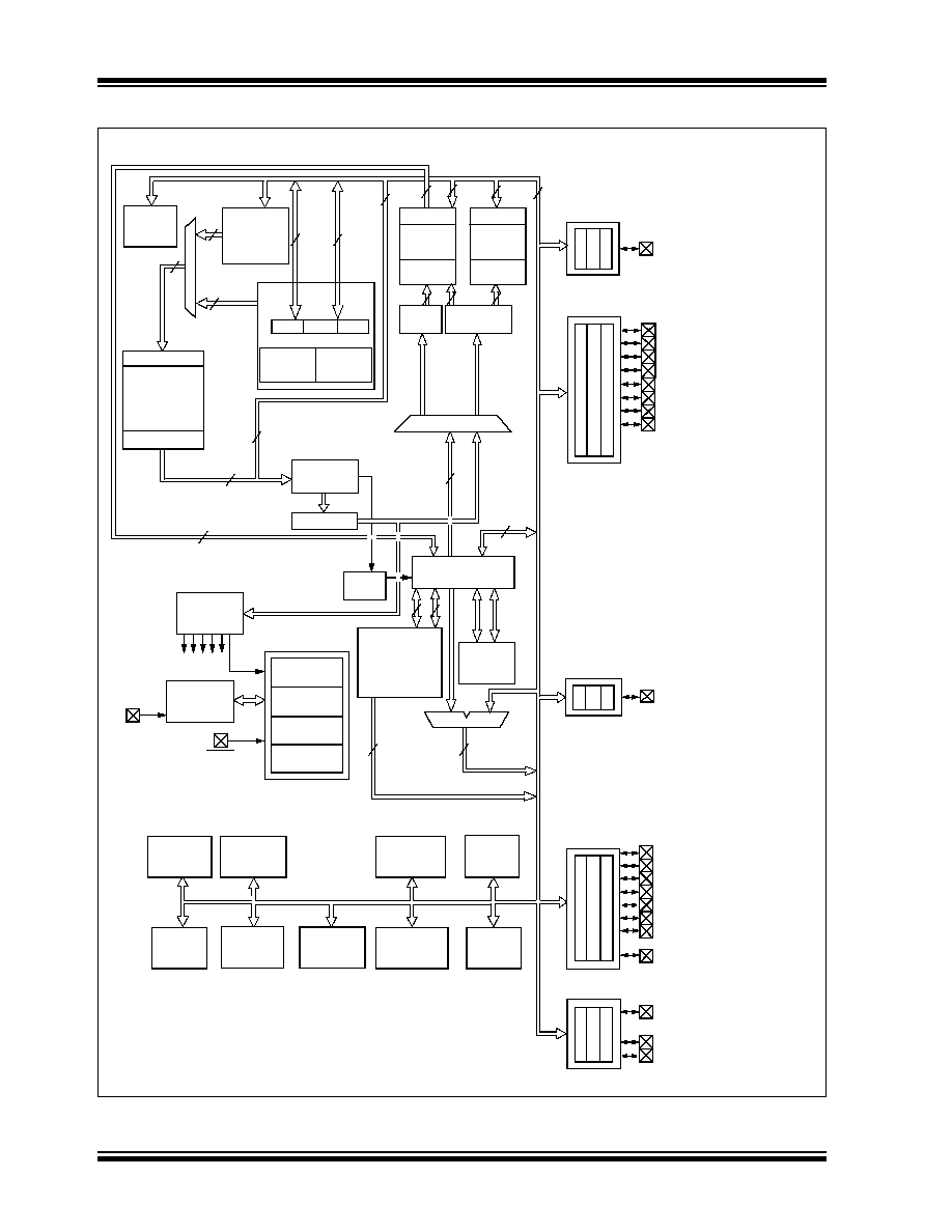
FIGURE 1-1:
dsPIC30F1010 BLOCK DIAGRAM
Power-up
Timer
Oscillator
Start-up Timer
POR
Reset
Watchdog
Timer
Instruction
Decode &
Control
OSC1/CLK1
MCLR
AN4/CMP2C/CN6/RB4
UART1
SPI1
SMPS
PWM
Timing
Generation
AN5/CMP2D/CN7/RB5
16
PCH PCL
Program Counter
ALU<16>
16
Address Latch
Program Memory
(12 Kbytes)
Data Latch
24
24
24
24
X Data Bus
IR
I
2
CTM
Comparator
PCU
PWM1L/RE0
PWM1H/RE1
PWM2L/RE2
PWM2H/RE3
RE4
10-bit ADC
Timers
RE5
PGC1/EMUC1/EXTREF/T1CK/
Output
Compare
Module
SFLT2/INT0/OCFLTA/RA9
PORTB
PGC/EMUC/SDI1/SDA/U1RX/RF7
PGD/EMUD/SD01/SCL/U1TX/RF8
PORTF
PORTD
16
16
16
16 x 16
W Reg Array
Divide
Unit
Engine
DSP
Decode
ROM Latch
16
Y Data Bus
Effective Address
X RAGU
X WAGU
Y AGU
AN0/CMP1A/CN2/RB0
AN1/CMP1B/CN3/RB1
AN2/CMP1C/CMP2A/CN4/RB2
AN3/CMP1D/CMP2B/CN5/RB3
16
16
16
16
16
PORTA
PORTE
16
16
16
16
8
Interrupt
Controller
PSV & Table
Data Access
Control Block
Stack
Control
Logic
Loop
Control
Logic
Data Latch
Data Latch
Y Data
(256 bytes)
RAM
X Data
(256 bytes)
RAM
Address
Latch
Address
Latch
Control Signals
to Various Blocks
PGC2/EMUC2/OC1/SFLT1/
16
16
OSC1/CLKI/RB6
OSC2/CLKO/RB7
INT1/RD0
PGD2/EMUD2/SCK1/SFLT3/
INT2/RF6
PGD1/EMUD1/T2CK/U1ATX/
Module
Input
Change
Notification
U1ARX/CN0/RE6
CN1/RE7

©
2006 Microchip Technology Inc.
Advance Information
DS70178A-page 11
dsPIC30F1010/202X
Table 1-1 provides a brief description of device I/O
pinouts for the dsPIC30F1010 and the functions that
may be multiplexed to a port pin. Multiple functions may
exist on one port pin. When multiplexing occurs, the
peripheral module's functional requirements may force
an override of the data direction of the port pin.
TABLE 1-1:
PINOUT I/O DESCRIPTIONS FOR dsPIC30F1010
Pin Name
Pin
Type
Buffer
Type
Description
AN0-AN5
I
Analog
Analog input channels.
AV
DD
P
P
Positive supply for analog module.
AV
SS
P
P
Ground reference for analog module.
CLKI
CLKO
I
O
ST/CMOS
--
External clock source input. Always associated with OSC1 pin function.
Oscillator crystal output. Connects to crystal or resonator in Crystal
Oscillator mode. Optionally functions as CLKO in RC and EC modes. Always
associated with OSC2 pin function.
EMUD
EMUC
EMUD1
EMUC1
EMUD2
EMUC2
I/O
I/O
I/O
I/O
I/O
I/O
ST
ST
ST
ST
ST
ST
ICD Primary Communication Channel data input/output pin.
ICD Primary Communication Channel clock input/output pin.
ICD Secondary Communication Channel data input/output pin.
ICD Secondary Communication Channel clock input/output pin.
ICD Tertiary Communication Channel data input/output pin.
ICD Tertiary Communication Channel clock input/output pin.
INT0
INT1
INT2
I
I
I
ST
ST
ST
External interrupt 0
External interrupt 1
External interrupt 2
SFLT1
SFLT2
SFLT3
PWM1L
PWM1H
PWM2L
PWM2H
I
I
I
O
O
O
O
ST
ST
ST
--
--
--
--
Shared Fault Pin 1
Shared Fault Pin 2
Shared Fault Pin 3
PWM 1 Low output
PWM 1 High output
PWM 2 Low output
PWM 2 High output
MCLR
I/P
ST
Master Clear (Reset) input or programming voltage input. This pin is an active
low Reset to the device.
OC1
O
--
Compare outputs.
OCFLTA
I
ST
Output Compare Fault Pin
OSC1
OSC2
I
I/O
CMOS
--
Oscillator crystal input.
Oscillator crystal output. Connects to crystal or resonator in Crystal Oscillator
mode. Optionally functions as CLKO in FRC and EC modes.
PGD
PGC
PGD1
PGC1
PGD2
PGC2
I/O
I
I/O
I
I/0
I
ST
ST
ST
ST
ST
ST
In-Circuit Serial ProgrammingTM data input/output pin.
In-Circuit Serial Programming clock input pin.
In-Circuit Serial Programming data input/output pin 1.
In-Circuit Serial Programming clock input pin 1.
In-Circuit Serial Programming data input/output pin 2.
In-Circuit Serial Programming clock input pin 2.
RB0-RB7
I/O
ST
PORTB is a bidirectional I/O port.
RA9
I/O
ST
PORTA is a bidirectional I/O port.
RD0
I/O
ST
PORTD is a bidirectional I/O port.
Legend:
CMOS = CMOS compatible input or output
Analog = Analog input
ST
= Schmitt Trigger input with CMOS levels
O
= Output
I
= Input P
= Power

dsPIC30F1010/202X
DS70178A-page 12
Advance Information
©
2006 Microchip Technology Inc.
RE0-RE7
I/O
ST
PORTE is a bidirectional I/O port.
RF6, RF7,
RF8
I/O
ST
PORTF is a bidirectional I/O port.
SCK1
SDI1
SDO1
SS1
I/O
I
O
I
ST
ST
--
ST
Synchronous serial clock input/output for SPI #1.
SPI #1 Data In.
SPI #1 Data Out.
SPI #1 Slave Synchronization.
SCL
SDA
I/O
I/O
ST
ST
Synchronous serial clock input/output for I
2
CTM.
Synchronous serial data input/output for I
2
C.
T1CK
T2CK
I
I
ST
ST
Timer1 external clock input.
Timer2 external clock input.
U1RX
U1TX
U1ARX
U1ATX
I
O
I
O
ST
--
ST
--
UART1 Receive.
UART1 Transmit.
Alternate UART1 Receive.
Alternate UART1 Transmit.
CMP1A
CMP1B
CMP1C
CMP1D
CMP2A
CMP2B
CMP2C
CMP2D
I
I
I
I
I
I
I
I
Analog
Analog
Analog
Analog
Analog
Analog
Analog
Analog
Comparator 1 Channel A
Comparator 1 Channel B
Comparator 1 Channel C
Comparator 1 Channel D
Comparator 2 Channel A
Comparator 2 Channel B
Comparator 2 Channel C
Comparator 2 Channel D
CN0-CN7
I
ST
Input Change notification inputs
Can be software programmed for internal weak pull-ups on all inputs.
V
DD
P
--
Positive supply for logic and I/O pins.
V
SS
P
--
Ground reference for logic and I/O pins.
V
REF
+
I
Analog
Analog Voltage Reference (High) input.
V
REF
-
I
Analog
Analog Voltage Reference (Low) input.
EXTREF
I
Analog
External reference to Comparator DAC
TABLE 1-1:
PINOUT I/O DESCRIPTIONS FOR dsPIC30F1010 (CONTINUED)
Pin Name
Pin
Type
Buffer
Type
Description
Legend:
CMOS = CMOS compatible input or output
Analog = Analog input
ST
= Schmitt Trigger input with CMOS levels
O
= Output
I
= Input P
= Power

©
2006 Microchip Technology Inc.
Advance Information
DS70178A-page 13
dsPIC30F1010/202X
FIGURE 1-2:
dsPIC30F2020 BLOCK DIAGRAM
Power-up
Timer
Oscillator
Start-up Timer
POR
Reset
Watchdog
Timer
Instruction
Decode &
Control
OSC1/CLK1
MCLR
AN4/CMP2C/CMP3A/CN6/RB4
UART1
SPI1
SMPS
PWM
Timing
Generation
AN5/CMP2D/CMP3B/CN7/RB5
16
PCH PCL
Program Counter
ALU<16>
16
Address Latch
Program Memory
(12 Kbytes)
Data Latch
24
24
24
24
X Data Bus
IR
I
2
CTM
Comparator
PCU
PWM1L/RE0
PWM1H/RE1
PWM2L/RE2
PWM2H/RE3
PWM3L/RE4
10-bit ADC
Timers
PWM3H/RE5
PGC1/EMUC1/EXTREF/PWM4L/
Input
Capture
Module
Output
Compare
Module
SFLT2/INT0/OCFLTA/RA9
PORTB
PGC/EMUC/SDI1/SDA/U1RX/RF7
PGD/EMUD/SD01/SCL/U1TX/RF8
PORTF
PORTD
16
16
16
16 x 16
W Reg Array
Divide
Unit
Engine
DSP
Decode
ROM Latch
16
Y Data Bus
Effective Address
X RAGU
X WAGU
Y AGU
AN0/CMP1A/CN2/RB0
AN1/CMP1B/CN3/RB1
AN2/CMP1C/CMP2A/CN4/RB2
AN3/CMP1D/CMP2B/CN5/RB3
16
16
16
16
16
PORTA
PORTE
16
16
16
16
8
Interrupt
Controller
PSV & Table
Data Access
Control Block
Stack
Control
Logic
Loop
Control
Logic
Data Latch
Data Latch
Y Data
(256 bytes)
RAM
X Data
(256 bytes)
RAM
Address
Latch
Address
Latch
Control Signals
to Various Blocks
PGC2/EMUC2/OC1/SFLT1/IC1/
16
16
AN6/CMP3C/CMP4A/
AN7/CMP3D/CMP4B/
CLKI/OSC1/RB6
CLKO/OSC2/RB7
INT1/RD0
PGD2/EMUD2/SCK1/SFLT3/OC2/
INT2/RF6
PGD1/EMUD1/PWM4H/T2CK/
Module
Input
Change
Notification
U1ARX/CN0/RE6
U1ATX/CN1/RE7
T1CK/

dsPIC30F1010/202X
DS70178A-page 14
Advance Information
©
2006 Microchip Technology Inc.
Table 1-2 provides a brief description of device I/O
pinouts for the dsPIC30F2020 and the functions that
may be multiplexed to a port pin. Multiple functions may
exist on one port pin. When multiplexing occurs, the
peripheral module's functional requirements may force
an override of the data direction of the port pin.
TABLE 1-2:
PINOUT I/O DESCRIPTIONS FOR dsPIC30F2020
Pin Name
Pin
Type
Buffer
Type
Description
AN0-AN7
I
Analog
Analog input channels.
AV
DD
P
P
Positive supply for analog module.
AV
SS
P
P
Ground reference for analog module.
CLKI
CLKO
I
O
ST/CMOS
--
External clock source input. Always associated with OSC1 pin function.
Oscillator crystal output. Connects to crystal or resonator in Crystal
Oscillator mode. Optionally functions as CLKO in RC and EC modes. Always
associated with OSC2 pin function.
EMUD
EMUC
EMUD1
EMUC1
EMUD2
EMUC2
I/O
I/O
I/O
I/O
I/O
I/O
ST
ST
ST
ST
ST
ST
ICD Primary Communication Channel data input/output pin.
ICD Primary Communication Channel clock input/output pin.
ICD Secondary Communication Channel data input/output pin.
ICD Secondary Communication Channel clock input/output pin.
ICD Tertiary Communication Channel data input/output pin.
ICD Tertiary Communication Channel clock input/output pin.
IC1
I
ST
Capture input.
INT0
INT1
INT2
I
I
I
ST
ST
ST
External interrupt 0
External interrupt 1
External interrupt 2
SFLT1
SFLT2
SFLT3
PWM1L
PWM1H
PWM2L
PWM2H
PWM3L
PWM3H
PWM4L
PWM4H
I
I
I
O
O
O
O
O
O
O
O
ST
ST
ST
--
--
--
--
--
--
--
--
Shared Fault Pin 1
Shared Fault Pin 2
Shared Fault Pin 3
PWM 1 Low output
PWM 1 High output
PWM 2 Low output
PWM 2 High output
PWM 3 Low output
PWM 3 High output
PWM 4 Low output
PWM 4 High output
MCLR
I/P
ST
Master Clear (Reset) input or programming voltage input. This pin is an active
low Reset to the device.
OC1-OC2
OCFLTA
O
I
--
Compare outputs.
Output Compare Fault pin
OSC1
OSC2
I
I/O
CMOS
--
Oscillator crystal input.
Oscillator crystal output. Connects to crystal or resonator in Crystal Oscillator
mode. Optionally functions as CLKO in FRC and EC modes.
PGD
PGC
PGD1
PGC1
PGD2
PGC2
I/O
I
I/O
I
I/O
I
ST
ST
ST
ST
ST
ST
In-Circuit Serial ProgrammingTM data input/output pin.
In-Circuit Serial Programming clock input pin.
In-Circuit Serial Programming data input/output pin 1.
In-Circuit Serial Programming clock input pin 1.
In-Circuit Serial Programming data input/output pin 2.
In-Circuit Serial Programming clock input pin 2.
Legend:
CMOS = CMOS compatible input or output
Analog = Analog input
ST
= Schmitt Trigger input with CMOS levels
O
= Output
I
= Input P
= Power

©
2006 Microchip Technology Inc.
Advance Information
DS70178A-page 15
dsPIC30F1010/202X
RB0-RB7
I/O
ST
PORTB is a bidirectional I/O port.
RA9
I/O
ST
PORTA is a bidirectional I/O port.
RD0
I/O
ST
PORTD is a bidirectional I/O port.
RE0-RE7
I/O
ST
PORTE is a bidirectional I/O port.
RF6, RF7,
RF8
I/O
ST
PORTF is a bidirectional I/O port.
SCK1
SDI1
SDO1
SS1
I/O
I
O
I
ST
ST
--
ST
Synchronous serial clock input/output for SPI #1.
SPI #1 Data In.
SPI #1 Data Out.
SPI #1 Slave Synchronization.
SCL
SDA
I/O
I/O
ST
ST
Synchronous serial clock input/output for I
2
CTM.
Synchronous serial data input/output for I
2
C.
T1CK
T2CK
I
I
ST
ST
Timer1 external clock input.
Timer2 external clock input.
U1RX
U1TX
U1ARX
U1ATX
I
O
I
O
ST
--
ST
O
UART1 Receive.
UART1 Transmit.
Alternate UART1 Receive.
Alternate UART1 Transmit.
CMP1A
CMP1B
CMP1C
CMP1D
CMP2A
CMP2B
CMP2C
CMP2D
CMP3A
CMP3B
CMP3C
CMP3D
CMP4A
CMP4B
I
I
I
I
I
I
I
I
I
I
I
I
I
I
Analog
Analog
Analog
Analog
Analog
Analog
Analog
Analog
Analog
Analog
Analog
Analog
Analog
Analog
Comparator 1 Channel A
Comparator 1 Channel B
Comparator 1 Channel C
Comparator 1 Channel D
Comparator 2 Channel A
Comparator 2 Channel B
Comparator 2 Channel C
Comparator 2 Channel D
Comparator 3 Channel A
Comparator 3 Channel B
Comparator 3 Channel C
Comparator 3 Channel D
Comparator 4 Channel A
Comparator 4 Channel B
CN0-CN7
I
ST
Input Change notification inputs
Can be software programmed for internal weak pull-ups on all inputs.
V
DD
P
--
Positive supply for logic and I/O pins.
V
SS
P
--
Ground reference for logic and I/O pins.
V
REF
+
I
Analog
Analog Voltage Reference (High) input.
V
REF
-
I
Analog
Analog Voltage Reference (Low) input.
EXTREF
I
Analog
External reference to Comparator DAC
TABLE 1-2:
PINOUT I/O DESCRIPTIONS FOR dsPIC30F2020 (CONTINUED)
Pin Name
Pin
Type
Buffer
Type
Description
Legend:
CMOS = CMOS compatible input or output
Analog = Analog input
ST
= Schmitt Trigger input with CMOS levels
O
= Output
I
= Input P
= Power

dsPIC30F1010/202X
DS70178A-page 16
Advance Information
©
2006 Microchip Technology Inc.
FIGURE 1-3:
dsPIC30F2023 BLOCK DIAGRAM
Power-up
Timer
Oscillator
Start-up Timer
POR
Reset
Watchdog
Timer
Instruction
Decode &
Control
OSC1/CLK1
MCLR
AN4/CMP2C/CMP3A/CN6/RB4
UART1
SPI1
SMPS
PWM
Timing
Generation
AN5/CMP2D/CMP3B/CN7/RB5
16
PCH PCL
Program Counter
ALU<16>
16
Address Latch
Program Memory
(12 Kbytes)
Data Latch
24
24
24
24
X Data Bus
IR
I
2
CTM
Comparator
PCU
PWM1L/RE0
PWM1H/RE1
PWM2L/RE2
PWM2H/RE3
PWM3L/RE4
10-bit ADC
Timers
PWM3H/RE5
PGC1/EMUC1/PWM4L/T1CK/
Input
Capture
Module
Output
Compare
Module
PORTB
SCL/RG2
SDA/RG3
PORTG
PORTD
16
16
16
16 x 16
W Reg Array
Divide
Unit
Engine
DSP
Decode
ROM Latch
16
Y Data Bus
Effective Address
X RAGU
X WAGU
Y AGU
EMUD3/AN0/CMP1A/CN2/RB0
EMUC3/AN1/CMP1B/CN3/RB1
AN2/CMP1C/CMP2A/CN4/RB2
AN3/CMP1D/CMP2B/CN5/RB3
16
16
16
16
16
PORTA
PORTE
16
16
16
16
8
Interrupt
Controller
PSV & Table
Data Access
Control Block
Stack
Control
Logic
Loop
Control
Logic
Data Latch
Data Latch
Y Data
(256 bytes)
RAM
X Data
(256 bytes)
RAM
Address
Latch
Address
Latch
Control Signals
to Various Blocks
OC2/RD1
16
16
AN6/CMP3C/CMP4A/
AN7/CMP3D/CMP4B/
OSC1/CLKI/RB6
OSC2/CLKO/RB7
PGD1/EMUD1/PWM4H/T2CK/
Module
SFLT1/RA8
SFLT2/INT0/OCFLTA/RA9
SFLT3/RA10
PGC/EMUC/SDI1/RF7
PGD/EMUD/SD01/RF8
PORTF
PGD2/EMUD2/SCK1/INT2/RF6
AN8/CMP4C/RB8
AN9/EXTREF/CMP4D/RB9
AN10/IFLT4/RB10
AN11/IFLT2/RB11
SYNCI/RF14
PGC2/EMUC2/OC1/IC1/INT1/
SFLT4/RA11
SYNCO/SSI/RF15
U1TX/RF3
U1RX/RF2
Input
Change
Notification
U1ARX/CN0/RE6
U1ATX/CN1/RE7
RD0

©
2006 Microchip Technology Inc.
Advance Information
DS70178A-page 17
dsPIC30F1010/202X
Table 1-3 provides a brief description of device I/O
pinouts for the dsPIC30F2023 and the functions that
may be multiplexed to a port pin. Multiple functions may
exist on one port pin. When multiplexing occurs, the
peripheral module's functional requirements may force
an override of the data direction of the port pin.
TABLE 1-3:
PINOUT I/O DESCRIPTIONS FOR dsPIC30F2023
Pin Name
Pin
Type
Buffer
Type
Description
AN0-AN11
I
Analog
Analog input channels.
AV
DD
P
P
Positive supply for analog module.
AV
SS
P
P
Ground reference for analog module.
CLKI
CLKO
I
O
ST/CMOS
--
External clock source input. Always associated with OSC1 pin function.
Oscillator crystal output. Connects to crystal or resonator in Crystal
Oscillator mode. Optionally functions as CLKO in RC and EC modes. Always
associated with OSC2 pin function.
EMUD
EMUC
EMUD1
EMUC1
EMUD2
EMUC2
I/O
I/O
I/O
I/O
I/O
I/O
ST
ST
ST
ST
ST
ST
ICD Primary Communication Channel data input/output pin.
ICD Primary Communication Channel clock input/output pin.
ICD Secondary Communication Channel data input/output pin.
ICD Secondary Communication Channel clock input/output pin.
ICD Tertiary Communication Channel data input/output pin.
ICD Tertiary Communication Channel clock input/output pin.
IC1
I
ST
Capture input.
INT0
INT1
INT2
I
I
I
ST
ST
ST
External interrupt 0
External interrupt 1
External interrupt 2
SFLT1
SFLT2
SFLT3
SFLT4
IFLT2
IFLT4
PWM1L
PWM1H
PWM2L
PWM2H
PWM3L
PWM3H
PWM4L
PWM4H
I
I
I
I
I
I
O
O
O
O
O
O
O
O
ST
ST
ST
ST
ST
ST
--
--
--
--
--
--
--
--
Shared Fault 1
Shared Fault 2
Shared Fault 3
Shared Fault 4
Independent Fault 2
Independent Fault 4
PWM 1 Low output
PWM 1 High output
PWM 2 Low output
PWM 2 High output
PWM 3 Low output
PWM 3 High output
PWM 4 Low output
PWM 4 High output
SYNCO
SYNCI
O
I
--
ST
PWM SYNC output
PWM SYNC input
MCLR
I/P
ST
Master Clear (Reset) input or programming voltage input. This pin is an active
low Reset to the device.
OC1-OC2
OCFLTA
O
I
--
ST
Compare outputs.
Output Compare Fault condition.
OSC1
OSC2
I
I/O
CMOS
--
Oscillator crystal input.
Oscillator crystal output. Connects to crystal or resonator in Crystal Oscillator
mode. Optionally functions as CLKO in FRC and EC modes.
Legend:
CMOS = CMOS compatible input or output
Analog = Analog input
ST
= Schmitt Trigger input with CMOS levels
O
= Output
I
= Input P
= Power

dsPIC30F1010/202X
DS70178A-page 18
Advance Information
©
2006 Microchip Technology Inc.
PGD
PGC
PGD1
PGC1
PGD2
PGC2
I/O
I
I/O
I
I/O
I
ST
ST
ST
ST
ST
ST
In-Circuit Serial ProgrammingTM data input/output pin.
In-Circuit Serial Programming clock input pin.
In-Circuit Serial Programming data input/output pin 1.
In-Circuit Serial Programming clock input pin 1.
In-Circuit Serial Programming data input/output pin 2.
In-Circuit Serial Programming clock input pin 2.
RA0,RA8-
RA11
I/O
ST
PORTA is a bidirectional I/O port.
RB0-RB11
I/O
ST
PORTB is a bidirectional I/O port.
RD0,RD1
I/O
ST
PORTD is a bidirectional I/O port.
RE0-RE7
I/O
ST
PORTE is a bidirectional I/O port.
RF2, RF3,
RF6-RF8,
RF14, RF15
I/O
ST
PORTF is a bidirectional I/O port.
RG2, RG3
I/O
ST
PORTG is a bidirectional I/O port.
SCK1
SDI1
SDO1
SS1
I/O
I
O
I
ST
ST
--
ST
Synchronous serial clock input/output for SPI #1.
SPI #1 Data In.
SPI #1 Data Out.
SPI #1 Slave Synchronization.
SCL
SDA
I/O
I/O
ST
ST
Synchronous serial clock input/output for I
2
C.
Synchronous serial data input/output for I
2
C.
T1CK
T2CK
I
I
ST
ST
Timer1 external clock input.
Timer2 external clock input.
U1RX
U1TX
U1ARX
U1ATX
I
O
I
O
ST
--
ST
--
UART1 Receive.
UART1 Transmit.
Alternate UART1 Receive.
Alternate UART1 Transmit
CMP1A
CMP1B
CMP1C
CMP1D
CMP2A
CMP2B
CMP2C
CMP2D
CMP3A
CMP3B
CMP3C
CMP3D
CMP4A
CMP4B
CMP4C
CMP4D
I
I
I
I
I
I
I
I
I
I
I
I
I
I
I
I
Analog
Analog
Analog
Analog
Analog
Analog
Analog
Analog
Analog
Analog
Analog
Analog
Analog
Analog
Analog
Analog
Comparator 1 Channel A
Comparator 1 Channel B
Comparator 1 Channel C
Comparator 1 Channel D
Comparator 2 Channel A
Comparator 2 Channel B
Comparator 2 Channel C
Comparator 2 Channel D
Comparator 3 Channel A
Comparator 3 Channel B
Comparator 3 Channel C
Comparator 3 Channel D
Comparator 4 Channel A
Comparator 4 Channel B
Comparator 4 Channel C
Comparator 4 Channel D
CN0-CN7
I
ST
Input Change notification inputs
Can be software programmed for internal weak pull-ups on all inputs.
V
DD
P
--
Positive supply for logic and I/O pins.
V
SS
P
--
Ground reference for logic and I/O pins.
V
REF
+
I
Analog
Analog Voltage Reference (High) input.
TABLE 1-3:
PINOUT I/O DESCRIPTIONS FOR dsPIC30F2023 (CONTINUED)
Pin Name
Pin
Type
Buffer
Type
Description
Legend:
CMOS = CMOS compatible input or output
Analog = Analog input
ST
= Schmitt Trigger input with CMOS levels
O
= Output
I
= Input P
= Power

©
2006 Microchip Technology Inc.
Advance Information
DS70178A-page 19
dsPIC30F1010/202X
V
REF
-
I
Analog
Analog Voltage Reference (Low) input.
EXTREF
I
Analog
External reference to Comparator DAC
TABLE 1-3:
PINOUT I/O DESCRIPTIONS FOR dsPIC30F2023 (CONTINUED)
Pin Name
Pin
Type
Buffer
Type
Description
Legend:
CMOS = CMOS compatible input or output
Analog = Analog input
ST
= Schmitt Trigger input with CMOS levels
O
= Output
I
= Input P
= Power

dsPIC30F1010/202X
DS70178A-page 20
Advance Information
©
2006 Microchip Technology Inc.
NOTES:

©
2006 Microchip Technology Inc.
Advance Information
DS70178A-page 21
dsPIC30F1010/202X
2.0
CPU ARCHITECTURE
OVERVIEW
This document provides a summary of the
dsPIC30F1010/202X CPU and peripheral function. For
a complete description of this functionality, please refer
to the "dsPIC30F Family Reference Manual"
(DS70046).
2.1
Core Overview
The core has a 24-bit instruction word. The Program
Counter (PC) is 23 bits wide with the Least Significant
bit (LSb) always clear (see Section 3.1 "Program
Address Space"), and the Most Significant bit (MSb)
is ignored during normal program execution, except for
certain specialized instructions. Thus, the PC can
address up to 4M instruction words of user program
space. An instruction prefetch mechanism is used to
help maintain throughput. Program loop constructs,
free from loop count management overhead, are sup-
ported using the
DO
and
REPEAT
instructions, both of
which are interruptible at any point.
The working register array consists of 16x16-bit regis-
ters, each of which can act as data, address or offset
registers. One working register (W15) operates as a
software Stack Pointer for interrupts and calls.
The data space is 64 Kbytes (32K words) and is split
into two blocks, referred to as X and Y data memory.
Each block has its own independent Address Genera-
tion Unit (AGU). Most instructions operate solely
through the X memory AGU, which provides the
appearance of a single unified data space. The
Multiply-Accumulate (
MAC
) class of dual source DSP
instructions operate through both the X and Y AGUs,
splitting the data address space into two parts (see
Section 3.2 "Data Address Space"). The X and Y
data space boundary is device-specific and cannot be
altered by the user. Each data word consists of 2 bytes,
and most instructions can address data either as words
or bytes.
There are two methods of accessing data stored in
program memory:
∑ The upper 32 Kbytes of data space memory can be
mapped into the lower half (user space) of program
space at any 16K program word boundary, defined
by the 8-bit Program Space Visibility Page
(PSVPAG) register. This lets any instruction access
program space as if it were data space, with a limita-
tion that the access requires an additional cycle.
Moreover, only the lower 16 bits of each instruction
word can be accessed using this method.
∑ Linear indirect access of 32K word pages within
program space is also possible using any working
register, via table read and write instructions.
Table read and write instructions can be used to
access all 24 bits of an instruction word.
Overhead-free circular buffers (modulo addressing) are
supported in both X and Y address spaces. This is pri-
marily intended to remove the loop overhead for DSP
algorithms.
The X AGU also supports Bit-Reversed Addressing
mode on destination effective addresses, to greatly
simplify input or output data reordering for radix-2 FFT
algorithms. Refer to Section 4.0 "Address Generator
Units" for details on modulo and Bit-Reversed
Addressing.
The core supports Inherent (no operand), Relative, Lit-
eral, Memory Direct, Register Direct, Register Indirect,
Register Offset and Literal Offset Addressing modes.
Instructions are associated with predefined Addressing
modes, depending upon their functional requirements.
For most instructions, the core is capable of executing
a data (or program data) memory read, a working reg-
ister (data) read, a data memory write and a program
(instruction) memory read per instruction cycle. As a
result, 3-operand instructions are supported, allowing
C = A + B operations to be executed in a single cycle.
A DSP engine has been included to significantly
enhance the core arithmetic capability and throughput.
It features a high-speed 17-bit by 17-bit multiplier, a
40-bit ALU, two 40-bit saturating accumulators and a
40-bit bidirectional barrel shifter. Data in the accumula-
tor or any working register can be shifted up to 15 bits
right or 16 bits left in a single cycle. The DSP instruc-
tions operate seamlessly with all other instructions and
have been designed for optimal real-time performance.
The
MAC
class of instructions can concurrently fetch
two data operands from memory, while multiplying two
W registers. To enable this concurrent fetching of data
operands, the data space has been split for these
instructions and linear for all others. This has been
achieved in a transparent and flexible manner, by
dedicating certain working registers to each address
space for the
MAC
class of instructions.
The core does not support a multi-stage instruction
pipeline. However, a single stage instruction prefetch
mechanism is used, which accesses and partially
decodes instructions a cycle ahead of execution, in
order to maximize available execution time. Most
instructions execute in a single cycle, with certain
exceptions.
The core features a vectored exception processing
structure for traps and interrupts, with 62 independent
vectors. The exceptions consist of up to 8 traps (of
which 4 are reserved) and 54 interrupts. Each interrupt
is prioritized based on a user-assigned priority between
1 and 7 (1 being the lowest priority and 7 being the
highest) in conjunction with a predetermined `natural
order'. Traps have fixed priorities, ranging from 8 to 15.
Note: This data sheet summarizes features of this group
of dsPIC30F devices and is not intended to be a complete
reference source. For more information on the CPU,
peripherals, register descriptions and general device
functionality, refer to the "dsPIC30F Family Reference
Manual" (DS70046). For more information on the device
instruction set and programming, refer to the "dsPIC30F/
33F Programmer's Reference Manual" (DS70157).

dsPIC30F1010/202X
DS70178A-page 22
Advance Information
©
2006 Microchip Technology Inc.
2.2
Programmer's Model
The programmer's model is shown in Figure 2-1 and
consists of 16x16-bit working registers (W0 through
W15), 2x40-bit accumulators (AccA and AccB),
STATUS register (SR), Data Table Page register
(TBLPAG), Program Space Visibility Page register
(PSVPAG), DO and REPEAT registers (DOSTART,
DOEND, DCOUNT and RCOUNT), and Program
Counter (PC). The working registers can act as data,
address or offset registers. All registers are memory
mapped. W0 acts as the W register for file register
addressing.
Some of these registers have a shadow register asso-
ciated with each of them, as shown in Figure 2-1. The
shadow register is used as a temporary holding register
and can transfer its contents to or from its host register
upon the occurrence of an event. None of the shadow
registers are accessible directly. The following rules
apply for transfer of registers into and out of shadows.
∑
PUSH.S
and
POP.S
W0, W1, W2, W3, SR (DC, N, OV, Z and C bits
only) are transferred.
∑
DO
instruction
DOSTART, DOEND, DCOUNT shadows are
pushed on loop start, and popped on loop end.
When a byte operation is performed on a working reg-
ister, only the Least Significant Byte (LSB) of the target
register is affected. However, a benefit of memory
mapped working registers is that both the Least and
Most Significant Bytes (MSBs) can be manipulated
through byte wide data memory space accesses.
2.2.1
SOFTWARE STACK POINTER/
FRAME POINTER
The dsPIC
Æ
DSC devices contain a software stack.
W15 is the dedicated software Stack Pointer (SP), and
will be automatically modified by exception processing
and subroutine calls and returns. However, W15 can be
referenced by any instruction in the same manner as all
other W registers. This simplifies the reading, writing
and manipulation of the Stack Pointer (e.g., creating
stack frames).
W15 is initialized to 0x0800 during a Reset. The user
may reprogram the SP during initialization to any
location within data space.
W14 has been dedicated as a Stack Frame Pointer as
defined by the
LNK
and
ULNK
instructions. However,
W14 can be referenced by any instruction in the same
manner as all other W registers.
2.2.2
STATUS REGISTER
The dsPIC DSC core has a 16-bit STATUS Register
(SR), the LSB of which is referred to as the SR Low
Byte (SRL) and the MSB as the SR High Byte (SRH).
See Figure 2-1 for SR layout.
SRL contains all the MCU ALU operation status flags
(including the Z bit), as well as the CPU Interrupt Prior-
ity Level Status bits, IPL<2:0>, and the REPEAT active
Status bit, RA. During exception processing, SRL is
concatenated with the MSB of the PC to form a
complete word value, which is then stacked.
The upper byte of the STATUS register contains the
DSP Adder/Subtracter status bits, the DO Loop Active
bit (DA) and the Digit Carry (DC) Status bit.
2.2.3
PROGRAM COUNTER
The Program Counter is 23 bits wide. Bit 0 is always
clear. Therefore, the PC can address up to 4M
instruction words.
Note:
In order to protect against misaligned
stack accesses, W15<0> is always clear.
©
2006 Microchip Technology Inc.
Advance Information
DS70178A-page 23
dsPIC30F1010/202X
FIGURE 2-1:
PROGRAMMER'S MODEL
TABPAG
PC22
PC0
7
0
D0
D15
Program Counter
Data Table Page Address
STATUS Register
Working Registers
DSP Operand
Registers
W1
W2
W3
W4
W5
W6
W7
W8
W9
W10
W11
W12/DSP Offset
W13/DSP Write Back
W14/Frame Pointer
W15/Stack Pointer
DSP Address
Registers
AD39
AD0
AD31
DSP
Accumulators
AccA
AccB
PSVPAG
7
0
Program Space Visibility Page Address
Z
0
OA
OB
SA
SB
RCOUNT
15
0
REPEAT Loop Counter
DCOUNT
15
0
DO Loop Counter
DOSTART
22
0
DO Loop Start Address
IPL2 IPL1
SPLIM
Stack Pointer Limit Register
AD15
SRL
PUSH.S Shadow
DO Shadow
OAB SAB
15
0
Core Configuration Register
Legend
CORCON
DA
DC
RA N
TBLPAG
PSVPAG
IPL0
OV
W0/WREG
SRH
DO Loop End Address
DOEND
22
C
dsPIC30F1010/202X
DS70178A-page 24
Advance Information
©
2006 Microchip Technology Inc.
2.3
Divide Support
The dsPIC DSC devices feature a 16/16-bit signed
fractional divide operation, as well as 32/16-bit and 16/
16-bit signed and unsigned integer divide operations, in
the form of single instruction iterative divides. The
following instructions and data sizes are supported:
1.
DIVF
≠ 16/16 signed fractional divide
2.
DIV.sd
≠ 32/16 signed divide
3.
DIV.ud
≠ 32/16 unsigned divide
4.
DIV.sw
≠ 16/16 signed divide
5.
DIV.uw
≠ 16/16 unsigned divide
The 16/16 divides are similar to the 32/16 (same number
of iterations), but the dividend is either zero-extended or
sign-extended during the first iteration.
The divide instructions must be executed within a
REPEAT loop. Any other form of execution (e.g. a
series of discrete divide instructions) will not function
correctly because the instruction flow depends on
RCOUNT. The divide instruction does not automatically
set up the RCOUNT value, and it must, therefore, be
explicitly and correctly specified in the
REPEAT
instruc-
tion, as shown in Table 2-1 (
REPEAT
will execute the
target instruction {operand value + 1} times). The
REPEAT loop count must be set up for 18 iterations of
the
DIV/DIVF
instruction. Thus, a complete divide
operation requires 19 cycles.
TABLE 2-1:
DIVIDE INSTRUCTIONS
Note:
The Divide flow is interruptible. However,
the user needs to save the context as
appropriate.
Instruction
Function
DIVF
Signed fractional divide: Wm/Wn
W0; Rem
W1
DIV.sd
Signed divide: (Wm + 1:Wm)/Wn
W0; Rem
W1
DIV.sw (or DIV.s)
Signed divide: Wm / Wn
W0; Rem
W1
DIV.ud
Unsigned divide: (Wm + 1:Wm)/Wn
W0; Rem
W1
DIV.uw (or DIV.u)
Unsigned divide: Wm / Wn
W0; Rem
W1

©
2006 Microchip Technology Inc.
Advance Information
DS70178A-page 25
dsPIC30F1010/202X
2.4
DSP Engine
The DSP engine consists of a high speed 17-bit x
17-bit multiplier, a barrel shifter, and a 40-bit adder/sub-
tracter (with two target accumulators, round and
saturation logic).
The DSP engine also has the capability to perform inher-
ent accumulator-to-accumulator operations, which
require no additional data. These instructions are
ADD,
SUB
and
NEG
.
The DSP engine has various options selected through
various bits in the CPU Core Configuration Register
(CORCON), as listed below:
1.
Fractional or integer DSP multiply (IF).
2.
Signed or unsigned DSP multiply (US).
3.
Conventional or convergent rounding (RND).
4.
Automatic saturation on/off for AccA (SATA).
5.
Automatic saturation on/off for AccB (SATB).
6.
Automatic saturation on/off for writes to data
memory (SATDW).
7.
Accumulator Saturation mode selection
(ACCSAT).
A block diagram of the DSP engine is shown in
Figure 2-2.
Note:
For CORCON layout, see Table 3-3.
TABLE 2-2:
DSP INSTRUCTION SUMMARY
Instruction
Algebraic Operation
ACC WB?
CLR
A = 0
Yes
ED
A = (x ≠ y)
2
No
EDAC
A = A + (x ≠ y)
2
No
MAC
A = A + (x * y)
Yes
MAC
A = A + x
2
No
MOVSAC
No change in A
Yes
MPY
A = x * y
No
MPY.N
A = ≠ x * y
No
MSC
A = A ≠ x * y
Yes

dsPIC30F1010/202X
DS70178A-page 26
Advance Information
©
2006 Microchip Technology Inc.
FIGURE 2-2:
DSP ENGINE BLOCK DIAGRAM
Zero Backfill
Sign-Extend
Barrel
Shifter
40-bit Accumulator A
40-bit Accumulator B
Round
Logic
X Da
t
a
Bus
To/From W Array
Adder
Saturate
Negate
32
32
33
16
16
16
16
40
40
40
40
S
a
t
u
r
a
t
e
Y Dat
a
Bu
s
40
Carry/Borrow Out
Carry/Borrow In
16
40
Multiplier/Scaler
17-bit

©
2006 Microchip Technology Inc.
Advance Information
DS70178A-page 27
dsPIC30F1010/202X
2.4.1
MULTIPLIER
The 17x17-bit multiplier is capable of signed or
unsigned operation and can multiplex its output using a
scaler to support either 1.31 fractional (Q31) or 32-bit
integer results. Unsigned operands are zero-extended
into the 17th bit of the multiplier input value. Signed
operands are sign-extended into the 17th bit of the mul-
tiplier input value. The output of the 17x17-bit multiplier/
scaler is a 33-bit value, which is sign-extended to 40
bits. Integer data is inherently represented as a signed
two's complement value, where the MSB is defined as
a sign bit. Generally speaking, the range of an N-bit
two's complement integer is -2
N-1
to 2
N-1
≠ 1. For a 16-
bit integer, the data range is -32768 (0x8000) to 32767
(0x7FFF), including 0. For a 32-bit integer, the data
range is -2,147,483,648 (0x8000 0000) to
2,147,483,645 (0x7FFF FFFF).
When the multiplier is configured for fractional multipli-
cation, the data is represented as a two's complement
fraction, where the MSB is defined as a sign bit and the
radix point is implied to lie just after the sign bit (QX for-
mat). The range of an N-bit two's complement fraction
with this implied radix point is -1.0 to (1-2
1-N
). For a
16-bit fraction, the Q15 data range is -1.0 (0x8000) to
0.999969482 (0x7FFF), including 0, and has a preci-
sion of 3.01518x10
-5
. In Fractional mode, a 16x16 mul-
tiply operation generates a 1.31 product, which has a
precision of 4.65661x10
-10
.
The same multiplier is used to support the MCU multi-
ply instructions, which include integer 16-bit signed,
unsigned and mixed sign multiplies.
The
MUL
instruction may be directed to use byte or
word sized operands. Byte operands will direct a 16-bit
result, and word operands will direct a 32-bit result to
the specified register(s) in the W array.
2.4.2
DATA ACCUMULATORS AND
ADDER/SUBTRACTER
The data accumulator consists of a 40-bit adder/
subtracter with automatic sign extension logic. It can
select one of two accumulators (A or B) as its pre-
accumulation source and post-accumulation destina-
tion. For the
ADD
and
LAC
instructions, the data to be
accumulated or loaded can be optionally scaled via the
barrel shifter, prior to accumulation.
2.4.2.1
Adder/Subtracter, Overflow and
Saturation
The adder/subtracter is a 40-bit adder with an optional
zero input into one side and either true or complement
data into the other input. In the case of addition, the
carry/borrow input is active high and the other input is
true data (not complemented), whereas in the case of
subtraction, the carry/borrow input is active low and the
other input is complemented. The adder/subtracter
generates overflow Status bits SA/SB and OA/OB,
which are latched and reflected in the STATUS register.
∑ Overflow from bit 39: this is a catastrophic
overflow in which the sign of the accumulator is
destroyed.
∑ Overflow into guard bits 32 through 39: this is a
recoverable overflow. This bit is set whenever all
the guard bits are not identical to each other.
The adder has an additional saturation block which
controls accumulator data saturation, if selected. It
uses the result of the adder, the overflow Status bits
described above, and the SATA/B (CORCON<7:6>)
and ACCSAT (CORCON<4>) mode control bits to
determine when and to what value to saturate.
Six STATUS register bits have been provided to
support saturation and overflow; they are:
1.
OA:
AccA overflowed into guard bits
2.
OB:
AccB overflowed into guard bits
3.
SA:
AccA saturated (bit 31 overflow and saturation)
or
AccA overflowed into guard bits and saturated
(bit 39 overflow and saturation)
4.
SB:
AccB saturated (bit 31 overflow and saturation)
or
AccB overflowed into guard bits and saturated
(bit 39 overflow and saturation)
5.
OAB:
Logical OR of OA and OB
6.
SAB:
Logical OR of SA and SB
The OA and OB bits are modified each time data
passes through the adder/subtracter. When set, they
indicate that the most recent operation has overflowed
into the accumulator guard bits (bits 32 through 39).
The OA and OB bits can also optionally generate an
arithmetic warning trap when set and the correspond-
ing overflow trap flag enable bit (OVATEN, OVBTEN) in
the INTCON1 register (refer to Section 5.0 "Inter-
rupts") is set. This allows the user to take immediate
action, for example, to correct system gain.

dsPIC30F1010/202X
DS70178A-page 28
Advance Information
©
2006 Microchip Technology Inc.
The SA and SB bits are modified each time data passes
through the adder/subtracter, but can only be cleared by
the user. When set, they indicate that the accumulator
has overflowed its maximum range (bit 31 for 32-bit sat-
uration, or bit 39 for 40-bit saturation) and will be satu-
rated (if saturation is enabled). When saturation is not
enabled, SA and SB default to bit 39 overflow and thus
indicate that a catastrophic overflow has occurred. If the
COVTE bit in the INTCON1 register is set, SA and SB
bits will generate an arithmetic warning trap when
saturation is disabled.
The overflow and saturation Status bits can optionally
be viewed in the STATUS Register (SR) as the logical
OR of OA and OB (in bit OAB) and the logical OR of SA
and SB (in bit SAB). This allows programmers to check
one bit in the STATUS Register to determine if either
accumulator has overflowed, or one bit to determine if
either accumulator has saturated. This is useful for
complex number arithmetic, which typically uses both
the accumulators.
The device supports three Saturation and Overflow
modes.
1.
Bit 39 Overflow and Saturation:
When bit 39 overflow and saturation occurs, the
saturation logic loads the maximally positive 9.31
(0x7FFFFFFFFF) or maximally negative 9.31
value (0x8000000000) into the target accumula-
tor. The SA or SB bit is set and remains set until
cleared by the user. This is referred to as `super
saturation' and provides protection against erro-
neous data or unexpected algorithm problems
(e.g., gain calculations).
2.
Bit 31 Overflow and Saturation:
When bit 31 overflow and saturation occurs, the
saturation logic then loads the maximally positive
1.31 value (0x007FFFFFFF) or maximally nega-
tive 1.31 value (0x0080000000) into the target
accumulator. The SA or SB bit is set and remains
set until cleared by the user. When this Saturation
mode is in effect, the guard bits are not used (so
the OA, OB or OAB bits are never set).
3.
Bit 39 Catastrophic Overflow
The bit 39 overflow Status bit from the adder is
used to set the SA or SB bit, which remain set
until cleared by the user. No saturation operation
is performed and the accumulator is allowed to
overflow (destroying its sign). If the COVTE bit in
the INTCON1 register is set, a catastrophic
overflow can initiate a trap exception.
2.4.2.2
Accumulator `Write Back'
The
MAC
class of instructions (with the exception of
MPY,
MPY.N,
ED
and
EDAC
) can optionally write a
rounded version of the high word (bits 31 through 16)
of the accumulator that is not targeted by the instruction
into data space memory. The write is performed across
the X bus into combined X and Y address space. The
following addressing modes are supported:
1.
W13, Register Direct:
The rounded contents of the non-target
accumulator are written into W13 as a 1.15
fraction.
2.
[W13] + = 2, Register Indirect with Post-Incre-
ment: The rounded contents of the non-target
accumulator are written into the address pointed
to by W13 as a 1.15 fraction. W13 is then
incremented by 2 (for a word write).
2.4.2.3
Round Logic
The round logic is a combinational block, which per-
forms a conventional (biased) or convergent (unbiased)
round function during an accumulator write (store). The
Round mode is determined by the state of the RND bit
in the CORCON register. It generates a 16-bit, 1.15 data
value which is passed to the data space write saturation
logic. If rounding is not indicated by the instruction, a
truncated 1.15 data value is stored and the least
significant word (lsw) is simply discarded.
Conventional rounding takes bit 15 of the accumulator,
zero-extends it and adds it to the ACCxH word (bits 16
through 31 of the accumulator). If the ACCxL word (bits
0 through 15 of the accumulator) is between 0x8000
and 0xFFFF (0x8000 included), ACCxH is incre-
mented. If ACCxL is between 0x0000 and 0x7FFF,
ACCxH is left unchanged. A consequence of this
algorithm is that over a succession of random rounding
operations, the value will tend to be biased slightly
positive.
Convergent (or unbiased) rounding operates in the
same manner as conventional rounding, except when
ACCxL equals 0x8000. If this is the case, the LSb (bit
16 of the accumulator) of ACCxH is examined. If it is `
1
',
ACCxH is incremented. If it is `
0
', ACCxH is not modi-
fied. Assuming that bit 16 is effectively random in
nature, this scheme will remove any rounding bias that
may accumulate.
The
SAC
and
SAC.R
instructions store either a trun-
cated (
SAC
) or rounded (
SAC.R
) version of the contents
of the target accumulator to data memory, via the X bus
(subject to data saturation, see Section 2.4.2.4 "Data
Space Write Saturation"). Note that for the
MAC
class
of instructions, the accumulator write back operation
will function in the same manner, addressing combined
MCU (X and Y) data space though the X bus. For this
class of instructions, the data is always subject to
rounding.

©
2006 Microchip Technology Inc.
Advance Information
DS70178A-page 29
dsPIC30F1010/202X
2.4.2.4
Data Space Write Saturation
In addition to adder/subtracter saturation, writes to data
space may also be saturated, but without affecting the
contents of the source accumulator. The data space
write saturation logic block accepts a 16-bit, 1.15 frac-
tional value from the round logic block as its input,
together with overflow status from the original source
(accumulator) and the 16-bit round adder. These are
combined and used to select the appropriate 1.15 frac-
tional value as output to write to data space memory.
If the SATDW bit in the CORCON register is set, data
(after rounding or truncation) is tested for overflow and
adjusted accordingly. For input data greater than
0x007FFF, data written to memory is forced to the max-
imum positive 1.15 value, 0x7FFF. For input data less
than 0xFF8000, data written to memory is forced to the
maximum negative 1.15 value, 0x8000. The MSb of the
source (bit 39) is used to determine the sign of the
operand being tested.
If the SATDW bit in the CORCON register is not set, the
input data is always passed through unmodified under
all conditions.
2.4.3
BARREL SHIFTER
The barrel shifter is capable of performing up to 15-bit
arithmetic or logic right shifts, or up to 16-bit left shifts
in a single cycle. The source can be either of the two
DSP accumulators or the X bus (to support multi-bit
shifts of register or memory data).
The shifter requires a signed binary value to determine
both the magnitude (number of bits) and direction of the
shift operation. A positive value will shift the operand
right. A negative value will shift the operand left. A
value of `
0
' will not modify the operand.
The barrel shifter is 40 bits wide, thereby obtaining a
40-bit result for DSP shift operations and a 16-bit result
for MCU shift operations. Data from the X bus is pre-
sented to the barrel shifter between bit positions 16 to
31 for right shifts, and bit positions 0 to 15 for left shifts.

dsPIC30F1010/202X
DS70178A-page 30
Advance Information
©
2006 Microchip Technology Inc.
NOTES:
©
2006 Microchip Technology Inc.
Advance Information
DS70178A-page 31
dsPIC30F1010/202X
3.0
MEMORY ORGANIZATION
3.1
Program Address Space
The program address space is 4M instruction words. It
is addressable by a 24-bit value from either the 23-bit
PC, table instruction Effective Address (EA), or data
space EA, when program space is mapped into data
space, as defined by Table 3-1. Note that the program
space address is incremented by two between succes-
sive program words, in order to provide compatibility
with data space addressing.
User program space access is restricted to the lower
4M instruction word address range (0x000000 to
0x7FFFFE), for all accesses other than
TBLRD/TBLWT
,
which use TBLPAG<7> to determine user or configura-
tion space access. In Table 3-1, Read/Write instruc-
tions, bit 23 allows access to the Device ID, the User ID
and the Configuration bits. Otherwise, bit 23 is always
clear.
FIGURE 3-1:
PROGRAM SPACE MEMORY
MAP FOR dsPIC30F1010/
202X
Note: This data sheet summarizes features of this group
of dsPIC30F devices and is not intended to be a complete
reference source. For more information on the CPU,
peripherals, register descriptions and general device
functionality, refer to the "dsPIC30F Family Reference
Manual" (DS70046). For more information on the device
instruction set and programming, refer to the "dsPIC30F/
33F Programmer's Reference Manual" (DS70157).
Note:
The address map shown in Figure 3-1 is
conceptual, and the actual memory con-
figuration may vary across individual
devices depending on available memory.
Reset ≠ Target Address
U
s
er
Me
mo
ry
Sp
a
c
e
000000
7FFFFE
00007E
Ext. Osc. Fail Trap
000002
000080
User Flash
Program Memory
002000
001FFE
Address Error Trap
Stack Error Trap
Arithmetic Warn. Trap
Reserved
Reserved
Reserved
Vector 0
Vector 1
Vector 52
Vector 53
(4K instructions)
Reserved
(Read
0
's)
0000FE
000100
000014
Alternate Vector Table
Reset ≠
GOTO
Instruction
000004
Reserved
Device Configuration
C
onf
i
g
ur
ati
o
n M
e
m
o
ry
Sp
a
c
e
800000
F80000
Registers
F8000E
F80010
DEVID (2)
FEFFFE
FF0000
FFFFFE
Reserved
F7FFFE
8005FE
800600
UNITID (32 instr.)
8005BE
8005C0
Reserved
Reserved
Vector Tables

dsPIC30F1010/202X
DS70178A-page 32
Advance Information
©
2006 Microchip Technology Inc.
TABLE 3-1:
PROGRAM SPACE ADDRESS CONSTRUCTION
FIGURE 3-2:
DATA ACCESS FROM PROGRAM SPACE ADDRESS GENERATION
Access Type
Access
Space
Program Space Address
<23>
<22:16>
<15>
<14:1>
<0>
Instruction Access
User
0
PC<22:1>
0
TBLRD/TBLWT
User
(TBLPAG<7> =
0
)
TBLPAG<7:0>
Data EA <15:0>
TBLRD/TBLWT
Configuration
(TBLPAG<7> =
1
)
TBLPAG<7:0>
Data EA <15:0>
Program Space Visibility
User
0
PSVPAG<7:0>
Data EA <14:0>
0
Program Counter
23 bits
1
PSVPAG Reg
8 bits
EA
15 bits
Program
Using
Select
TBLPAG Reg
8 bits
EA
16 bits
Using
Byte
24-bit EA
0
0
1/0
Select
User/
Configuration
Table
Instruction
Program
Space
Counter
Using
Space
Select
Note: Program Space Visibility cannot be used to access bits <23:16> of a word in program memory.
Visibility
©
2006 Microchip Technology Inc.
Advance Information
DS70178A-page 33
dsPIC30F1010/202X
3.1.1
DATA ACCESS FROM PROGRAM
MEMORY USING TABLE
INSTRUCTIONS
This architecture fetches 24-bit wide program memory.
Consequently, instructions are always aligned. How-
ever, as the architecture is modified Harvard, data can
also be present in program space.
There are two methods by which program space can
be accessed; via special table instructions, or through
the remapping of a 16K word program space page into
the upper half of data space (see Section 3.1.2 "Data
Access from Program Memory Using Program
Space Visibility"). The
TBLRDL
and
TBLWTL
instruc-
tions offer a direct method of reading or writing the least
significant word (lsw) of any address within program
space, without going through data space. The
TBLRDH
and
TBLWTH
instructions are the only method whereby
the upper 8 bits of a program space word can be
accessed as data.
The PC is incremented by two for each successive
24-bit program word. This allows program memory
addresses to directly map to data space addresses.
Program memory can thus be regarded as two 16-bit
word wide address spaces, residing side by side, each
with the same address range.
TBLRDL
and
TBLWTL
access the space which contains the Least Significant
Data Word, and
TBLRDH
and
TBLWTH
access the
space which contains the Most Significant Data Byte.
Figure 3-2 shows how the EA is created for table oper-
ations and data space accesses (PSV =
1
). Here,
P<23:0> refers to a program space word, whereas
D<15:0> refers to a data space word.
A set of Table Instructions is provided to move byte or
word sized data to and from program space.
1.
TBLRDL:
Table Read Low
Word: Read the lsw of the program address;
P<15:0> maps to D<15:0>.
Byte: Read one of the LSBs of the program
address;
P<7:0> maps to the destination byte when byte
select =
0
;
P<15:8> maps to the destination byte when byte
select =
1
.
2.
TBLWTL:
Table Write Low (refer to Section 7.0
"Flash Program Memory" for details on Flash
Programming).
3.
TBLRDH:
Table Read High
Word: Read the most significant word of the
program address;
P<23:16> maps to D<7:0>; D<15:8> always
be =
0
.
Byte: Read one of the MSBs of the program
address;
P<23:16> maps to the destination byte when
byte select =
0
;
The destination byte will always be =
0
when
byte select =
1
.
4.
TBLWTH:
Table Write High (refer to Section 7.0
"Flash Program Memory" for details on Flash
Programming).
FIGURE 3-3:
PROGRAM DATA TABLE ACCESS (LEAST SIGNIFICANT WORD)
0
8
16
PC Address
0x000000
0x000002
0x000004
0x000006
23
00000000
00000000
00000000
00000000
Program Memory
`Phantom' Byte
(Read as `
0
').
TBLRDL.W
TBLRDL.B (Wn<0> = 1)
TBLRDL.B (Wn<0> = 0)

dsPIC30F1010/202X
DS70178A-page 34
Advance Information
©
2006 Microchip Technology Inc.
FIGURE 3-4:
PROGRAM DATA TABLE ACCESS (MOST SIGNIFICANT BYTE)
3.1.2
DATA ACCESS FROM PROGRAM
MEMORY USING PROGRAM
SPACE VISIBILITY
The upper 32 Kbytes of data space may optionally be
mapped into any 16K word program space page. This
provides transparent access of stored constant data
from X data space, without the need to use special
instructions (i.e.,
TBLRDL/H, TBLWTL/H
instructions).
Program space access through the data space occurs
if the MSb of the data space EA is set and program
space visibility is enabled, by setting the PSV bit in the
Core Control register (CORCON). The functions of
CORCON are discussed in Section 2.4 "DSP
Engine".
Data accesses to this area add an additional cycle to
the instruction being executed, since two program
memory fetches are required.
Note that the upper half of addressable data space is
always part of the X data space. Therefore, when a
DSP operation uses program space mapping to access
this memory region, Y data space should typically con-
tain state (variable) data for DSP operations, whereas
X data space should typically contain coefficient
(constant) data.
Although each data space address, 0x8000 and higher,
maps directly into a corresponding program memory
address (see Figure 3-5), only the lower 16-bits of the
24-bit program word are used to contain the data. The
upper 8 bits should be programmed to force an illegal
instruction to maintain machine robustness. Refer to
the "dsPIC30F/33F Programmer's Reference Manual"
(DS70157) for details on instruction encoding.
Note that by incrementing the PC by 2 for each pro-
gram memory word, the Least Significant 15 bits of
data space addresses directly map to the Least Signif-
icant 15 bits in the corresponding program space
addresses. The remaining bits are provided by the Pro-
gram Space Visibility Page register, PSVPAG<7:0>, as
shown in Figure 3-5.
For instructions that use PSV which are executed
outside a REPEAT loop:
∑ The following instructions will require one instruc-
tion cycle in addition to the specified execution
time:
-
MAC
class of instructions with data operand
prefetch
-
MOV
instructions
-
MOV.D
instructions
∑ All other instructions will require two instruction
cycles in addition to the specified execution time
of the instruction.
For instructions that use PSV which are executed
inside a REPEAT loop:
∑ The following instances will require two instruction
cycles in addition to the specified execution time
of the instruction:
- Execution in the first iteration
- Execution in the last iteration
- Execution prior to exiting the loop due to an
interrupt
- Execution upon re-entering the loop after an
interrupt is serviced
∑ Any other iteration of the REPEAT loop will allow
the instruction, accessing data using PSV, to
execute in a single cycle.
0
8
16
PC Address
0x000000
0x000002
0x000004
0x000006
23
00000000
00000000
00000000
00000000
Program Memory
`Phantom' Byte
(Read as `
0
')
TBLRDH.W
TBLRDH.B (Wn<0> = 1)
TBLRDH.B (Wn<0> = 0)
Note:
PSV access is temporarily disabled during
Table Reads/Writes.

©
2006 Microchip Technology Inc.
Advance Information
DS70178A-page 35
dsPIC30F1010/202X
FIGURE 3-5:
DATA SPACE WINDOW INTO PROGRAM SPACE OPERATION
3.2
Data Address Space
The core has two data spaces. The data spaces can be
considered either separate (for some DSP instruc-
tions), or as one unified linear address range (for MCU
instructions). The data spaces are accessed using two
Address Generation Units (AGUs) and separate data
paths.
3.2.1
DATA SPACE MEMORY MAP
The data space memory is split into two blocks, X and
Y data space. A key element of this architecture is that
Y space is a subset of X space, and is fully contained
within X space. In order to provide an apparent linear
addressing space, X and Y spaces have contiguous
addresses.
When executing any instruction other than one of the
MAC
class of instructions, the X block consists of the
256 byte data address space (including all Y
addresses). When executing one of the
MAC
class of
instructions, the X block consists of the 256 bytes data
address space excluding the Y address block (for data
reads only). In other words, all other instructions regard
the entire data memory as one composite address
space. The
MAC
class instructions extract the Y
address space from data space and address it using
EAs sourced from W10 and W11. The remaining X data
space is addressed using W8 and W9. Both address
spaces are concurrently accessed only with the
MAC
class instructions.
A data space memory map is shown in Figure 3-6.
23
15
0
PSVPAG
(1)
15
15
EA<15> =
0
EA<15> =
1
16
Data
Space
EA
Data Space
Program Space
8
15
23
0x0000
0x8000
0xFFFF
0x00
0x100100
0x001FFE
Data Read
Upper half of Data
Space is mapped
into Program Space
Note: PSVPAG is an 8-bit register, containing bits <22:15> of the program space address
(i.e., it defines the page in program space to which the upper half of data space is being mapped).
0x001200
Address
Concatenation
BSET
CORCON,#2
; PSV bit set
MOV
#0x00, W0
; Set PSVPAG register
MOV
W0, PSVPAG
MOV
0x9200, W0
; Access program memory location
; using a data space access

dsPIC30F1010/202X
DS70178A-page 36
Advance Information
©
2006 Microchip Technology Inc.
FIGURE 3-6:
DATA SPACE MEMORY MAP
0x0000
0x07FE
0x08FE
0xFFFE
LSB
Address
16 bits
LSB
MSB
MSB
Address
0x0001
0x07FF
0x08FF
0xFFFF
0x8001
0x8000
Optionally
Mapped
into Program
Memory
0x09FF
0x09FE
0x0801
0x0800
0x0901
0x0900
Near
Data
SFR Space
512 bytes
SRAM Space
2560 bytes
Note:
Unimplemented SFR or SRAM locations read as `
0
'.
Space
Unimplemented (X)
X Data
SFR Space
X Data RAM (X)
Y Data RAM (Y)
(Note)
256 bytes
256 bytes
(See Note)
0x0A00

©
2006 Microchip Technology Inc.
Advance Information
DS70178A-page 37
dsPIC30F1010/202X
FIGURE 3-7:
DATA SPACE FOR MCU AND DSP (
MAC
CLASS) INSTRUCTIONS
SFR SPACE
(Y SPACE)
X SP
ACE
SFR SPACE
UNUSED
X
SPA
C
E
X SP
ACE
Y SPACE
UNUSED
UNUSED
Non-
MAC
Class Ops (Read/Write)
MAC
Class Ops Read-Only
Indirect EA using any W
Indirect EA using W8, W9
Indirect EA using W10, W11
MAC
Class Ops (Write)

dsPIC30F1010/202X
DS70178A-page 38
Advance Information
©
2006 Microchip Technology Inc.
3.2.2
DATA SPACES
The X data space is used by all instructions and sup-
ports all Addressing modes. There are separate read
and write data buses. The X read data bus is the return
data path for all instructions that view data space as
combined X and Y address space. It is also the X
address space data path for the dual operand read
instructions (
MAC
class). The X write data bus is the
only write path to data space for all instructions.
The X data space also supports modulo addressing for
all instructions, subject to Addressing mode restric-
tions. Bit-Reversed Addressing is only supported for
writes to X data space.
The Y data space is used in concert with the X data
space by the
MAC
class of instructions (
CLR,
ED,
EDAC,
MAC,
MOVSAC,
MPY,
MPY.N
and
MSC
) to pro-
vide two concurrent data read paths. No writes occur
across the Y bus. This class of instructions dedicates
two W register pointers, W10 and W11, to always
address Y data space, independent of X data space,
whereas W8 and W9 always address X data space.
Note that during accumulator write back, the data
address space is considered a combination of X and Y
data spaces, so the write occurs across the X bus.
Consequently, the write can be to any address in the
entire data space.
The Y data space can only be used for the data
prefetch operation associated with the
MAC
class of
instructions. It also supports modulo addressing for
automated circular buffers. Of course, all other instruc-
tions can access the Y data address space through the
X data path, as part of the composite linear space.
The boundary between the X and Y data spaces is
defined as shown in Figure 3-6 and is not user pro-
grammable. Should an EA point to data outside its own
assigned address space, or to a location outside phys-
ical memory, an all-zero word/byte will be returned. For
example, although Y address space is visible by all
non-
MAC
instructions using any Addressing mode, an
attempt by a
MAC
instruction to fetch data from that
space, using W8 or W9 (X space pointers), will return
0x0000.
TABLE 3-2:
EFFECT OF INVALID
MEMORY ACCESSES
All effective addresses are 16 bits wide and point to
bytes within the data space. Therefore, the data space
address range is 64 Kbytes or 32K words.
3.2.3
DATA SPACE WIDTH
The core data width is 16 bits. All internal registers are
organized as 16-bit wide words. Data space memory is
organized in byte addressable, 16-bit wide blocks.
3.2.4
DATA ALIGNMENT
To help maintain backward compatibility with
PICmicro
Æ
MCU devices and improve data space
memory usage efficiency, the dsPIC30F instruction set
supports both word and byte operations. Data is
aligned in data memory and registers as words, but all
data space EAs resolve to bytes. Data byte reads will
read the complete word, which contains the byte, using
the LSb of any EA to determine which byte to select.
The selected byte is placed onto the LSB of the X data
path (no byte accesses are possible from the Y data
path as the
MAC
class of instruction can only fetch
words). That is, data memory and registers are orga-
nized as two parallel byte-wide entities with shared
(word) address decode, but separate write lines. Data
byte writes only write to the corresponding side of the
array or register which matches the byte address.
As a consequence of this byte accessibility, all effective
address calculations (including those generated by the
DSP operations, which are restricted to word sized
data) are internally scaled to step through word-aligned
memory. For example, the core would recognize that
Post-Modified Register Indirect Addressing mode,
[Ws++], will result in a value of Ws + 1 for byte
operations and Ws + 2 for word operations.
All word accesses must be aligned to an even address.
Misaligned word data fetches are not supported, so
care must be taken when mixing byte and word opera-
tions, or translating from 8-bit MCU code. Should a mis-
aligned read or write be attempted, an address error
trap will be generated. If the error occurred on a read,
the instruction underway is completed, whereas if it
occurred on a write, the instruction will be executed but
the write will not occur. In either case, a trap will then
be executed, allowing the system and/or user to exam-
ine the machine state prior to execution of the address
fault.
FIGURE 3-8:
DATA ALIGNMENT
Attempted Operation
Data Returned
EA = an unimplemented address
0x0000
W8 or W9 used to access Y data
space in a
MAC
instruction
0x0000
W10 or W11 used to access X
data space in a
MAC
instruction
0x0000
15
8 7
0
0001
0003
0005
0000
0002
0004
Byte 1 Byte 0
Byte 3 Byte 2
Byte 5 Byte 4
LSB
MSB
©
2006 Microchip Technology Inc.
Advance Information
DS70178A-page 39
dsPIC30F1010/202X
All byte loads into any W register are loaded into the
LSB. The MSB is not modified.
A Sign-Extend (
SE
) instruction is provided to allow
users to translate 8-bit signed data to 16-bit signed
values. Alternatively, for 16-bit unsigned data, users
can clear the MSB of any W register by executing a
Zero-Extend (
ZE
) instruction on the appropriate
address.
Although most instructions are capable of operating on
word or byte data sizes, it should be noted that some
instructions, including the DSP instructions, operate
only on words.
3.2.5
NEAR DATA SPACE
An 8 Kbyte `near' data space is reserved in X address
memory space between 0x0000 and 0x1FFF, which is
directly addressable via a 13-bit absolute address field
within all memory direct instructions. The remaining X
address space and all of the Y address space is
addressable indirectly. Additionally, the whole of X data
space is addressable using
MOV
instructions, which
support memory direct addressing with a 16-bit
address field.
3.2.6
SOFTWARE STACK
The dsPIC DSC device contains a software stack. W15
is used as the Stack Pointer.
The Stack Pointer always points to the first available
free word and grows from lower addresses towards
higher addresses. It pre-decrements for stack pops and
post-increments for stack pushes, as shown in
Figure 3-9. Note that for a PC push during any
CALL
instruction, the MSB of the PC is zero-extended before
the push, ensuring that the MSB is always clear.
There is a Stack Pointer Limit register (SPLIM) associ-
ated with the Stack Pointer. SPLIM is uninitialized at
Reset. As is the case for the Stack Pointer, SPLIM<0>
is forced to `
0
', because all stack operations must be
word-aligned. Whenever an Effective Address (EA) is
generated using W15 as a source or destination
pointer, the address thus generated is compared with
the value in SPLIM. If the contents of the Stack Pointer
(W15) and the SPLIM register are equal and a push
operation is performed, a stack error trap will not occur.
The stack error trap will occur on a subsequent push
operation. Thus, for example, if it is desirable to cause
a stack error trap when the stack grows beyond
address 0x2000 in RAM, initialize the SPLIM with the
value, 0x1FFE.
Similarly, a Stack Pointer Underflow (stack error) trap is
generated when the Stack Pointer address is found to
be less than 0x0800, thus preventing the stack from
interfering with the Special Function Register (SFR)
space.
A write to the SPLIM register should not be immediately
followed by an indirect read operation using W15.
FIGURE 3-9:
CALL
STACK FRAME
Note:
A PC push during exception processing
will concatenate the SRL register to the
MSB of the PC prior to the push.
<Free Word>
PC<15:0>
000000000
0
15
W15 (before
CALL
)
W15 (after
CALL
)
S
t
a
ck G
r
o
w
s
T
o
wa
r
d
s
Highe
r A
ddr
es
s
PUSH
: [W15++]
POP
: [--W15]
0x0000
PC<22:16>

dsPIC30F1010/202X
DS70178A-page 40
Advance Information
©
2006 Microchip Technology Inc.
T
A
BLE
3
-
3
:
CORE
RE
GIS
T
E
R
MAP
S
F
R Nam
e
Ad
d
r
.
B
it
15
Bit
14
Bit 1
3
Bit
12
Bit
1
1
Bit
10
Bi
t 9
B
it 8
B
it
7
B
it 6
B
it 5
B
it
4
B
i
t
3
B
i
t
2
B
it
1
B
it
0
R
ese
t S
t
at
e
W
0
0
000
W0
/
WREG
0000 00
00 0000 0000
W
1
0
002
W1
0000 00
00 0000 0000
W
2
0
004
W2
0000 00
00 0000 0000
W
3
0
006
W3
0000 00
00 0000 0000
W
4
0
008
W4
0000 00
00 0000 0000
W
5
00
0A
W5
0000 00
00 0000 0000
W
6
000
C
W6
0000 00
00 0000 0000
W
7
00
0E
W7
0000 00
00 0000 0000
W
8
0
010
W8
0000 00
00 0000 0000
W
9
0
012
W9
0000 00
00 0000 0000
W
1
0
0
014
W1
0
0000 00
00 0000 0000
W
1
1
0
016
W1
1
0000 00
00 0000 0000
W
1
2
0
018
W1
2
0000 00
00 0000 0000
W1
3
0
0
1
A
W1
3
0000 00
00 0000 0000
W
1
4
001
C
W1
4
0000 00
00 0000 0000
W1
5
0
0
1
E
W1
5
0000 10
00 0000 0000
S
P
L
I
M
0
020
SPL
I
M
0000 00
00 0000 0000
ACCAL
0
0
2
2
AC
C
A
L
0000 00
00 0000 0000
ACCAH
0
0
2
4
ACCAH
0000 00
00 0000 0000
ACCAU
0
0
2
6
Sig
n
-
Exte
n
s
io
n
(
A
CCA<3
9
>
)
A
CCAU
0000 00
00 0000 0000
ACCBL
0
0
2
8
AC
C
B
L
0000 00
00 0000 0000
ACCBH
0
0
2
A
ACCBH
0000 00
00 0000 0000
ACCBU
0
0
2
C
S
ig
n
-
Exte
n
s
io
n
(
A
CCB<3
9
>
)
A
CCBU
0000 00
00 0000 0000
PCL
0
0
2
E
PCL
0000 00
00 0000 0000
P
C
H
0
030
--
--
--
--
--
--
--
--
--P
C
H
0000 00
00 0000 0000
T
B
LP
A
G
00
3
2
--
--
--
--
--
--
--
--T
B
L
P
A
G
0000 00
00 0000 0000
PS
VP
AG
0
0
3
4
--
--
--
--
--
--
--
--
PSVP
AG
0000 00
00 0000 0000
RCOUNT
0
0
3
6
RCO
UNT
uuuu uu
uu uuuu uuuu
DCOUNT
0
0
3
8
DCO
UNT
uuuu uu
uu uuuu uuuu
DO
ST
AR
TL
0
0
3
A
DO
ST
AR
TL
0
uuuu uu
uu uuuu uuu0
DO
ST
AR
TH
0
0
3
C
--
--
--
--
--
--
--
--
--D
O
S
T
A
R
T
H
0000 00
00 0uuu uuuu
DOENDL
0
0
3
E
DO
E
N
DL
0
uuuu uu
uu uuuu uuu0
DOENDH
0
0
4
0
--
--
--
--
--
--
--
--
--
D
OENDH
0000 00
00 0uuu uuuu
SR
0
0
4
2
O
A
O
B
SA
SB
O
A
B
SAB
DA
DC
I
P
L
2
I
P
L
1
I
P
L
0
RA
N
O
V
Z
C
0000 00
00 0000 0000
CORCO
N
0
0
4
4
--
--
--
U
S
E
DT
DL
2
D
L
1
DL
0
S
A
T
A
S
A
T
B
S
A
T
DW
ACCSA
T
IPL
3
PSV
RND
IF
0000 00
00 0010 0000
Le
gen
d:
u
= u
n
in
itia
li
z
e
d
b
i
t

©
2006 Microchip Technology Inc.
Advance Information
DS70178A-page 41
dsPIC30F1010/202X
Note
:
Ref
e
r to
th
e "
ds
PIC
3
0F F
a
mi
ly
R
e
fe
ren
c
e
Ma
nua
l"
(D
S7
004
6) f
o
r de
sc
rip
t
io
ns
of re
gi
ste
r
bi
t fi
eld
s
.
M
O
DCO
N
0
0
4
6
XM
O
D
EN
Y
M
O
D
EN
--
--
B
WM
<3
:
0
>
Y
WM
<3
:
0
>
X
WM
<3
:
0
>
0000 00
00 0000 0000
XM
O
D
SR
T
0
0
4
8
XS<1
5
:
1
>
0
uuuu uu
uu uuuu uuu0
XM
O
D
END
0
0
4
A
XE<1
5
:
1
>
1
uuuu uu
uu uuuu uuu1
YM
O
D
SR
T
0
0
4
C
YS<1
5
:
1
>
0
uuuu uu
uu uuuu uuu0
YM
O
D
END
0
0
4
E
YE<1
5
:
1
>
1
uuuu uu
uu uuuu uuu1
XB
R
E
V
0
0
5
0
B
R
EN
XB<1
4
:
0
>
uuuu uu
uu uuuu uuuu
DISICNT
0
0
5
2
--
--
D
IS
ICNT
<13:0
>
0000 00
00 0000 0000
T
A
BLE
3
-
3
:
CORE
RE
GIS
T
E
R
MAP
(
C
O
N
T
I
NUE
D
)
S
F
R Nam
e
Ad
d
r
.
B
it
15
Bit
14
Bit 1
3
Bit
12
Bit
1
1
Bit
10
Bi
t 9
B
it 8
B
it
7
B
it 6
B
it 5
B
it
4
B
i
t
3
B
i
t
2
B
it
1
B
it
0
R
ese
t S
t
at
e
Le
gen
d:
u
= u
n
in
itia
li
z
e
d
b
i
t

dsPIC30F1010/202X
DS70178A-page 42
Advance Information
©
2006 Microchip Technology Inc.
NOTES:
©
2006 Microchip Technology Inc.
Advance Information
DS70178A-page 43
dsPIC30F1010/202X
4.0
ADDRESS GENERATOR UNITS
The dsPIC DSC core contains two independent
address generator units: the X AGU and Y AGU. The Y
AGU supports word sized data reads for the DSP
MAC
class of instructions only. The dsPIC DSC AGUs
support three types of data addressing:
∑ Linear Addressing
∑ Modulo (Circular) Addressing
∑ Bit-Reversed Addressing
Linear and Modulo Data Addressing modes can be
applied to data space or program space. Bit-Reversed
Addressing is only applicable to data space addresses.
4.1
Instruction Addressing Modes
The Addressing modes in Table 4-1 form the basis of
the Addressing modes optimized to support the specific
features of individual instructions. The Addressing
modes provided in the
MAC
class of instructions are
somewhat different from those in the other instruction
types.
4.1.1
FILE REGISTER INSTRUCTIONS
Most file register instructions use a 13-bit address field
(f) to directly address data present in the first 8192
bytes of data memory (near data space). Most file
register instructions employ a working register, W0,
which is denoted as WREG in these instructions. The
destination is typically either the same file register, or
WREG (with the exception of the
MUL
instruction),
which writes the result to a register or register pair. The
MOV
instruction allows additional flexibility and can
access the entire data space.
TABLE 4-1:
FUNDAMENTAL ADDRESSING MODES SUPPORTED
Note: This data sheet summarizes features of this group
of dsPIC30F devices and is not intended to be a complete
reference source. For more information on the CPU,
peripherals, register descriptions and general device
functionality, refer to the "dsPIC30F Family Reference
Manual" (DS70046). For more information on the device
instruction set and programming, refer to the "dsPIC30F/
33F Programmer's Reference Manual" (DS70157).
Addressing Mode
Description
File Register Direct
The address of the file register is specified explicitly.
Register Direct
The contents of a register are accessed directly.
Register Indirect
The contents of Wn forms the EA.
Register Indirect Post-modified
The contents of Wn forms the EA. Wn is post-modified (incremented or
decremented) by a constant value.
Register Indirect Pre-modified
Wn is pre-modified (incremented or decremented) by a signed constant value
to form the EA.
Register Indirect with Register Offset The sum of Wn and Wb forms the EA.
Register Indirect with Literal Offset
The sum of Wn and a literal forms the EA.

dsPIC30F1010/202X
DS70178A-page 44
Advance Information
©
2006 Microchip Technology Inc.
4.1.2
MCU INSTRUCTIONS
The three-operand MCU instructions are of the form:
Operand 3 = Operand 1 <function> Operand 2
where Operand 1 is always a working register (i.e., the
Addressing mode can only be register direct), which is
referred to as Wb. Operand 2 can be a W register,
fetched from data memory, or a 5-bit literal. The result
location can be either a W register or an address
location. The following Addressing modes are
supported by MCU instructions:
∑ Register Direct
∑ Register Indirect
∑ Register Indirect Post-modified
∑ Register Indirect Pre-modified
∑ 5-bit or 10-bit Literal
4.1.3
MOVE AND ACCUMULATOR
INSTRUCTIONS
Move instructions and the DSP Accumulator class of
instructions provide a greater degree of addressing
flexibility than other instructions. In addition to the
Addressing modes supported by most MCU instruc-
tions, move and accumulator instructions also support
Register Indirect with Register Offset Addressing
mode, also referred to as Register Indexed mode.
In summary, the following Addressing modes are
supported by move and accumulator instructions:
∑ Register Direct
∑ Register Indirect
∑ Register Indirect Post-modified
∑ Register Indirect Pre-modified
∑ Register Indirect with Register Offset (Indexed)
∑ Register Indirect with Literal Offset
∑ 8-bit Literal
∑ 16-bit Literal
4.1.4
MAC
INSTRUCTIONS
The dual source operand DSP instructions (
CLR,
ED,
EDAC,
MAC,
MPY,
MPY.N,
MOVSAC
and
MSC
), also
referred to as
MAC
instructions, utilize a simplified set of
Addressing modes to allow the user to effectively
manipulate the data pointers through register indirect
tables.
The two source operand prefetch registers must be a
member of the set {W8, W9, W10, W11}. For data
reads, W8 and W9 will always be directed to the X
RAGU and W10 and W11 will always be directed to the
Y AGU. The effective addresses generated (before and
after modification) must, therefore, be valid addresses
within X data space for W8 and W9 and Y data space
for W10 and W11.
In summary, the following Addressing modes are
supported by the
MAC
class of instructions:
∑ Register Indirect
∑ Register Indirect Post-modified by 2
∑ Register Indirect Post-modified by 4
∑ Register Indirect Post-modified by 6
∑ Register Indirect with Register Offset (Indexed)
4.1.5
OTHER INSTRUCTIONS
Besides the various Addressing modes outlined above,
some instructions use literal constants of various sizes.
For example,
BRA
(branch) instructions use 16-bit
signed literals to specify the branch destination directly,
whereas the
DISI
instruction uses a 14-bit unsigned
literal field. In some instructions, such as
ADD
Acc
, the
source of an operand or result is implied by the opcode
itself. Certain operations, such as
NOP
, do not have any
operands.
Note:
Not all instructions support all the
Addressing modes given above. Individual
instructions may support different subsets
of these Addressing modes.
Note:
For the
MOV
instructions, the Addressing
mode specified in the instruction can differ
for the source and destination EA. How-
ever, the 4-bit Wb (Register Offset) field is
shared between both source and
destination (but typically only used by
one).
Note:
Not all instructions support all the
Addressing modes given above. Individual
instructions may support different subsets
of these Addressing modes.
Note:
Register Indirect with Register Offset
Addressing is only available for W9 (in X
space) and W11 (in Y space).

©
2006 Microchip Technology Inc.
Advance Information
DS70178A-page 45
dsPIC30F1010/202X
4.2
Modulo Addressing
Modulo addressing is a method of providing an auto-
mated means to support circular data buffers using
hardware. The objective is to remove the need for soft-
ware to perform data address boundary checks when
executing tightly looped code, as is typical in many
DSP algorithms.
Modulo addressing can operate in either data or pro-
gram space (since the data pointer mechanism is essen-
tially the same for both). One circular buffer can be
supported in each of the X (which also provides the
pointers into program space) and Y data spaces. Modulo
addressing can operate on any W register pointer. How-
ever, it is not advisable to use W14 or W15 for modulo
addressing, since these two registers are used as the
Stack Frame Pointer and Stack Pointer, respectively.
In general, any particular circular buffer can only be
configured to operate in one direction, as there are cer-
tain restrictions on the buffer start address (for incre-
menting buffers) or end address (for decrementing
buffers) based upon the direction of the buffer.
The only exception to the usage restrictions is for buff-
ers which have a power-of-2 length. As these buffers
satisfy the start and end address criteria, they may
operate in a Bidirectional mode, (i.e., address bound-
ary checks will be performed on both the lower and
upper address boundaries).
4.2.1
START AND END ADDRESS
The modulo addressing scheme requires that a
starting and an end address be specified and loaded
into the 16-bit modulo buffer address registers:
XMODSRT, XMODEND, YMODSRT and YMODEND
(see Table 3-3).
The length of a circular buffer is not directly specified. It
is determined by the difference between the corre-
sponding start and end addresses. The maximum
possible length of the circular buffer is 32K words
(64 Kbytes).
4.2.2
W ADDRESS REGISTER
SELECTION
The Modulo and Bit-Reversed Addressing Control reg-
ister MODCON<15:0> contains enable flags as well as
a W register field to specify the W address registers.
The XWM and YWM fields select which registers will
operate with modulo addressing. If XWM = 15, X RAGU
and X WAGU modulo addressing are disabled.
Similarly, if YWM = 15, Y AGU modulo addressing is
disabled.
The X Address Space Pointer W register (XWM) to
which modulo addressing is to be applied, is stored in
MODCON<3:0> (see Table 3-3). Modulo addressing is
enabled for X data space when XWM is set to any value
other than 15 and the XMODEN bit is set at
MODCON<15>.
The Y Address Space Pointer W register (YWM) to
which modulo addressing is to be applied, is stored in
MODCON<7:4>. Modulo addressing is enabled for Y
data space when YWM is set to any value other than 15
and the YMODEN bit is set at MODCON<14>.
Note:
Y-space modulo addressing EA calcula-
tions assume word sized data (LSb of
every EA is always clear).

dsPIC30F1010/202X
DS70178A-page 46
Advance Information
©
2006 Microchip Technology Inc.
FIGURE 4-1:
MODULO ADDRESSING OPERATION EXAMPLE
0x1100
0x1163
Start Addr = 0x1100
End Addr = 0x1163
Length = 0x0032 words
Byte
Address
MOV
#0x1100,W0
MOV
W0, XMODSRT
;set modulo start address
MOV
#0x1163,W0
MOV
W0,MODEND
;set modulo end address
MOV
#0x8001,W0
MOV
W0,MODCON
;enable W1, X AGU for modulo
MOV
#0x0000,W0
;W0 holds buffer fill value
MOV
#0x1110,W1
;point W1 to buffer
DO
AGAIN,#0x31
;fill the 50 buffer locations
MOV
W0, [W1++]
;fill the next location
AGAIN:
INC
W0,W0
;increment the fill value

©
2006 Microchip Technology Inc.
Advance Information
DS70178A-page 47
dsPIC30F1010/202X
4.2.3
MODULO ADDRESSING
APPLICABILITY
Modulo addressing can be applied to the Effective
Address (EA) calculation associated with any W regis-
ter. It is important to realize that the address bound-
aries check for addresses less than or greater than the
upper (for incrementing buffers) and lower (for decre-
menting buffers) boundary addresses (not just equal
to). Address changes may, therefore, jump beyond
boundaries and still be adjusted correctly.
4.3
Bit-Reversed Addressing
Bit-Reversed Addressing is intended to simplify data
re-ordering for radix-2 FFT algorithms. It is supported
by the X AGU for data writes only.
The modifier, which may be a constant value or register
contents, is regarded as having its bit order reversed.
The address source and destination are kept in normal
order. Thus, the only operand requiring reversal is the
modifier.
4.3.1
BIT-REVERSED ADDRESSING
IMPLEMENTATION
Bit-Reversed Addressing is enabled when:
1.
BWM (W register selection) in the MODCON
register is any value other than 15 (the stack can
not be accessed using Bit-Reversed
Addressing) and
2.
the BREN bit is set in the XBREV register and
3.
the Addressing mode used is Register Indirect
with Pre-Increment or Post-Increment.
If the length of a bit-reversed buffer is M = 2
N
bytes,
then the last `N' bits of the data buffer start address
must be zeros.
XB<14:0> is the bit-reversed address modifier or `pivot
point' which is typically a constant. In the case of an
FFT computation, its value is equal to half of the FFT
data buffer size.
When enabled, Bit-Reversed Addressing will only be
executed for register indirect with pre-increment or
post-increment addressing and word sized data writes.
It will not function for any other Addressing mode or for
byte sized data, and normal addresses will be gener-
ated instead. When Bit-Reversed Addressing is active,
the W Address Pointer will always be added to the
address modifier (XB) and the offset associated with
the register Indirect Addressing mode will be ignored.
In addition, as word sized data is a requirement, the
LSb of the EA is ignored (and always clear).
If Bit-Reversed Addressing has already been enabled
by setting the BREN (XBREV<15>) bit, then a write to
the XBREV register should not be immediately followed
by an indirect read operation using the W register that
has been designated as the bit-reversed pointer.
FIGURE 4-2:
BIT-REVERSED ADDRESS EXAMPLE
Note:
The modulo corrected effective address is
written back to the register only when Pre-
Modify or Post-Modify Addressing mode is
used to compute the Effective Address.
When an address offset (e.g., [W7 + W2])
is used, modulo address correction is per-
formed, but the contents of the register
remains unchanged.
Note:
All Bit-Reversed EA calculations assume
word sized data (LSb of every EA is
always clear). The XB value is scaled
accordingly to generate compatible (byte)
addresses.
Note:
Modulo addressing and Bit-Reversed
Addressing should not be enabled
together. In the event that the user
attempts to do this, Bit-Reversed Address-
ing will assume priority when active for the
X WAGU, and X WAGU modulo address-
ing will be disabled. However, modulo
addressing will continue to function in the
X RAGU.
b3 b2 b1 0
b2 b3 b4 0
Bit Locations Swapped Left-to-Right
Around Center of Binary Value
Bit-Reversed Address
XB = 0x0008 for a 16 word Bit-Reversed Buffer
b7 b6 b5 b1
b7 b6 b5 b4
b11 b10 b9 b8
b11 b10 b9 b8
b15 b14 b13 b12
b15 b14 b13 b12
Sequential Address
Pivot Point
dsPIC30F1010/202X
DS70178A-page 48
Advance Information
©
2006 Microchip Technology Inc.
TABLE 4-2:
BIT-REVERSED ADDRESS SEQUENCE (16-ENTRY)
TABLE 4-3:
BIT-REVERSED ADDRESS MODIFIER VALUES FOR XBREV REGISTER
Normal
Address
Bit-Reversed
Address
A3
A2
A1
A0
Decimal
A3
A2
A1
A0
Decimal
0
0
0
0
0
0
0
0
0
0
0
0
0
1
1
1
0
0
0
8
0
0
1
0
2
0
1
0
0
4
0
0
1
1
3
1
1
0
0
12
0
1
0
0
4
0
0
1
0
2
0
1
0
1
5
1
0
1
0
10
0
1
1
0
6
0
1
1
0
6
0
1
1
1
7
1
1
1
0
14
1
0
0
0
8
0
0
0
1
1
1
0
0
1
9
1
0
0
1
9
1
0
1
0
10
0
1
0
1
5
1
0
1
1
11
1
1
0
1
13
1
1
0
0
12
0
0
1
1
3
1
1
0
1
13
1
0
1
1
11
1
1
1
0
14
0
1
1
1
7
1
1
1
1
15
1
1
1
1
15
Buffer Size (Words)
XB<14:0> Bit-Reversed Address Modifier Value
(1)
32768
0x4000
16384
0x2000
8192
0x1000
4096
0x0800
2048
0x0400
1024
0x0200
512
0x0100
256
0x0080
128
0x0040
64
0x0020
32
0x0010
16
0x0008
8
0x0004
4
0x0002
2
0x0001
Note
1:
Modifier values greater than 256 words exceed the data memory available on the dsPIC30F1010/202X device

©
2006 Microchip Technology Inc.
Advance Information
DS70178A-page 49
dsPIC30F1010/202X
5.0
INTERRUPTS
The dsPIC30F1010/202X device has up to 35 interrupt
sources and 4 processor exceptions (traps), which
must be arbitrated based on a priority scheme.
The CPU is responsible for reading the Interrupt Vec-
tor Table (IVT) and transferring the address contained
in the interrupt vector to the Program Counter (PC).
The interrupt vector is transferred from the program
data bus into the Program Counter, via a 24-bit wide
multiplexer on the input of the Program Counter.
The Interrupt Vector Table and Alternate Interrupt Vec-
tor Table (AIVT) are placed near the beginning of pro-
gram memory (0x000004). The IVT and AIVT are
shown in Figure 5-1.
The interrupt controller is responsible for pre-
processing the interrupts and processor exceptions,
prior to their being presented to the processor core.
The peripheral interrupts and traps are enabled, priori-
tized and controlled using centralized special function
registers:
∑ IFS0<15:0>, IFS1<15:0>, IFS2<15:0>
All interrupt request flags are maintained in these
three registers. The flags are set by their respec-
tive peripherals or external signals, and they are
cleared via software.
∑ IEC0<15:0>, IEC1<15:0>, IEC2<15:0>
All interrupt enable control bits are maintained in
these three registers. These control bits are used
to individually enable interrupts from the
peripherals or external signals.
∑ IPC0<15:0>... IPC11<7:0>
The user-assignable priority level associated with
each of these interrupts is held centrally in these
twelve registers.
∑ IPL<3:0> The current CPU priority level is explic-
itly stored in the IPL bits. IPL<3> is present in the
CORCON register, whereas IPL<2:0> are present
in the STATUS Register (SR) in the processor
core.
∑ INTCON1<15:0>, INTCON2<15:0>
Global interrupt control functions are derived from
these two registers. INTCON1 contains the con-
trol and status flags for the processor exceptions.
The INTCON2 register controls the external inter-
rupt request signal behavior and the use of the
alternate vector table.
All interrupt sources can be user assigned to one of 7
priority levels, 1 through 7, via the IPCx registers.
Each interrupt source is associated with an interrupt
vector, as shown in Figure 5-1. Levels 7 and 1 repre-
sent the highest and lowest maskable priorities,
respectively.
If the NSTDIS bit (INTCON1<15>) is set, nesting of
interrupts is prevented. Thus, if an interrupt is currently
being serviced, processing of a new interrupt is
prevented, even if the new interrupt is of higher priority
than the one currently being serviced.
Certain interrupts have specialized control bits for
features like edge or level triggered interrupts, inter-
rupt-on-change, etc. Control of these features remains
within the peripheral module that generates the
interrupt.
The
DISI
instruction can be used to disable the
processing of interrupts of priorities 6 and lower for a
certain number of instructions, during which the DISI bit
(INTCON2<14>) remains set.
When an interrupt is serviced, the PC is loaded with the
address stored in the vector location in Program Mem-
ory that corresponds to the interrupt. There are 63 dif-
ferent vectors within the IVT (refer to Figure 5-1). These
vectors are contained in locations 0x000004 through
0x0000FE of program memory (refer to Figure 5-1).
These locations contain 24-bit addresses, and, in order
to preserve robustness, an address error trap will take
place should the PC attempt to fetch any of these
words during normal execution. This prevents execu-
tion of random data as a result of accidentally decre-
menting a PC into vector space, accidentally mapping
a data space address into vector space, or the PC roll-
ing over to 0x000000 after reaching the end of imple-
mented program memory space. Execution of a
GOTO
instruction to this vector space will also generate an
address error trap.
Note: This data sheet summarizes features of this group
of dsPIC30F devices and is not intended to be a complete
reference source. For more information on the CPU,
peripherals, register descriptions and general device
functionality, refer to the "dsPIC30F Family Reference
Manual" (DS70046). For more information on the device
instruction set and programming, refer to the "dsPIC30F/
33F Programmer's Reference Manual" (DS70157).
Note:
Interrupt flag bits get set when an Interrupt
condition occurs, regardless of the state of
its corresponding enable bit. User soft-
ware should ensure the appropriate inter-
rupt flag bits are clear prior to enabling an
interrupt.
Note:
Assigning a priority level of 0 to an inter-
rupt source is equivalent to disabling that
interrupt.
Note:
The IPL bits become read-only whenever
the NSTDIS bit has been set to `
1
'.

dsPIC30F1010/202X
DS70178A-page 50
Advance Information
©
2006 Microchip Technology Inc.
5.1
Interrupt Priority
The user-assignable Interrupt Priority (IP<2:0>) bits for
each individual interrupt source are located in the Least
Significant 3 bits of each nibble, within the IPCx
register(s). Bit 3 of each nibble is not used and is read
as a `
0
'. These bits define the priority level assigned to
a particular interrupt by the user.
Since more than one interrupt request source may be
assigned to a specific user specified priority level, a
means is provided to assign priority within a given level.
This method is called "Natural Order Priority" and is
final.
Natural order priority is determined by the position of an
interrupt in the vector table, and only affects interrupt
operation when multiple interrupts with the same user-
assigned priority become pending at the same time.
Table 5-1 lists the interrupt numbers and interrupt
sources for the dsPIC DSC devices and their
associated vector numbers.
The ability for the user to assign every interrupt to one
of seven priority levels implies that the user can assign
a very high overall priority level to an interrupt with a
low natural order priority. The INT0 (external interrupt
0) may be assigned to priority level 1, thus giving it a
very low effective priority.
TABLE 5-1:
dsPIC30F1010/202X
INTERRUPT VECTOR TABLE
Note:
The user selectable priority levels start at
0, as the lowest priority, and level 7, as the
highest priority.
Note 1: The natural order priority scheme has 0
as the highest priority and 53 as the
lowest priority.
2: The natural order priority number is the
same as the INT number.
INT
Number
Vector
Number
Interrupt Source
Highest Natural Order Priority
0
8
INT0 ≠ External Interrupt 0
1
9
IC1 ≠ Input Capture 1
2
10
OC1 ≠ Output Compare 1
3
11
T1 ≠ Timer 1
4
12
Reserved
5
13
OC2 ≠ Output Compare 2
6
14
T2 ≠ Timer 2
7
15
T3 ≠ Timer 3
8
16
SPI1
9
17
U1RX ≠ UART1 Receiver
10
18
U1TX ≠ UART1 Transmitter
11
19
ADC ≠ ADC Convert Done
12
20
NVM ≠ NVM Write Complete
13
21
SI2C ≠ I
2
CTM Slave Event
14
22
MI2C ≠ I
2
C Master Event
15
23
Reserved
16
24
INT1 ≠ External Interrupt 1
17
25
INT2 ≠ External Interrupt 2
18
26
PWM Special Event Trigger
19
27
PWM Gen#1
20
28
PWM Gen#2
21
29
PWM Gen#3
22
30
PWM Gen#4
23
31
Reserved
24
32
Reserved
25
33
Reserved
26
34
Reserved
27
35
ICN ≠ Input Change Notification
28
36
Reserved
29
37
Analog Comparator 1
30
38
Analog Comparator 2
31
39
Analog Comparator 3
32
40
Analog Comparator 4
33
41
Reserved
34
42
Reserved
35
43
Reserved
36
44
Reserved
37
45
ADC Pair 0 Conversion Done
38
46
ADC Pair 1 Conversion Done
39
47
ADC Pair 2 Conversion Done
40
48
ADC Pair 3 Conversion Done
41
49
ADC Pair 4 Conversion Done
42
50
ADC Pair 5 Conversion Done
43
51
Reserved
44
52
Reserved
45-53
53-61
Reserved
Lowest Natural Order Priority

©
2006 Microchip Technology Inc.
Advance Information
DS70178A-page 51
dsPIC30F1010/202X
5.2
Reset Sequence
A Reset is not a true exception, because the interrupt
controller is not involved in the Reset process. The pro-
cessor initializes its registers in response to a Reset,
which forces the PC to zero. The processor then begins
program execution at location 0x000000. A
GOTO
instruction is stored in the first program memory loca-
tion, immediately followed by the address target for the
GOTO
instruction. The processor executes the
GOTO
to
the specified address and then begins operation at the
specified target (start) address.
5.2.1
RESET SOURCES
In addition to External Reset and Power-on Reset
(POR), there are 6 sources of error conditions which
`trap' to the Reset vector.
∑ Watchdog Time-out:
The watchdog has timed out, indicating that the
processor is no longer executing the correct flow
of code.
∑ Uninitialized W Register Trap:
An attempt to use an uninitialized W register as
an Address Pointer will cause a Reset.
∑ Illegal Instruction Trap:
Attempted execution of any unused opcodes will
result in an illegal instruction trap. Note that a
fetch of an illegal instruction does not result in an
illegal instruction trap if that instruction is flushed
prior to execution due to a flow change.
∑ Trap Lockout:
Occurrence of multiple Trap conditions
simultaneously will cause a Reset.
5.3
Traps
Traps can be considered as non-maskable interrupts
indicating a software or hardware error, which adhere
to a predefined priority as shown in Figure 5-1. They
are intended to provide the user a means to correct
erroneous operation during debug and when operating
within the application.
Note that many of these trap conditions can only be
detected when they occur. Consequently, the question-
able instruction is allowed to complete prior to trap
exception processing. If the user chooses to recover
from the error, the result of the erroneous action that
caused the trap may have to be corrected.
There are 8 fixed priority levels for traps: Level 8
through Level 15, which implies that the IPL3 is always
set during processing of a trap.
If the user is not currently executing a trap, and he sets
the IPL<3:0> bits to a value of `
0111
' (Level 7), then all
interrupts are disabled, but traps can still be processed.
5.3.1
TRAP SOURCES
The following traps are provided with increasing prior-
ity. However, since all traps can be nested, priority has
little effect.
Math Error Trap:
The Math Error trap executes under the following four
circumstances:
1.
Should an attempt be made to divide by zero,
the divide operation will be aborted on a cycle
boundary and the trap taken.
2.
If enabled, a Math Error trap will be taken when
an arithmetic operation on either accumulator A
or B causes an overflow from bit 31 and the
accumulator guard bits are not utilized.
3.
If enabled, a Math Error trap will be taken when
an arithmetic operation on either accumulator A
or B causes a catastrophic overflow from bit 39
and all saturation is disabled.
4.
If the shift amount specified in a shift instruction
is greater than the maximum allowed shift
amount, a trap will occur.
Note:
If the user does not intend to take correc-
tive action in the event of a Trap Error con-
dition, these vectors must be loaded with
the address of a default handler that sim-
ply contains the
RESET
instruction. If, on
the other hand, one of the vectors contain-
ing an invalid address is called, an
address error trap is generated.
dsPIC30F1010/202X
DS70178A-page 52
Advance Information
©
2006 Microchip Technology Inc.
Address Error Trap:
This trap is initiated when any of the following
circumstances occurs:
1.
A misaligned data word access is attempted.
2.
A data fetch from our unimplemented data
memory location is attempted.
3.
A data access of an unimplemented program
memory location is attempted.
4.
An instruction fetch from vector space is
attempted.
5.
Execution of a "
BRA #litera
l" instruction or a
"
GOTO #literal
" instruction, where
literal
is an unimplemented program memory address.
6.
Executing instructions after modifying the PC to
point to unimplemented program memory
addresses. The PC may be modified by loading
a value into the stack and executing a
RETURN
instruction.
Stack Error Trap:
This trap is initiated under the following conditions:
1.
The Stack Pointer is loaded with a value which
is greater than the (user programmable) limit
value written into the SPLIM register (stack
overflow).
2.
The Stack Pointer is loaded with a value which
is less than 0x0800 (simple stack underflow).
Oscillator Fail Trap:
This trap is initiated if the external oscillator fails and
operation becomes reliant on an internal RC backup.
5.3.2
HARD AND SOFT TRAPS
It is possible that multiple traps can become active
within the same cycle (e.g., a misaligned word stack
write to an overflowed address). In such a case, the
fixed priority shown in Figure 5-1 is implemented,
which may require the user to check if other traps are
pending, in order to completely correct the fault.
`Soft' traps include exceptions of priority level 8 through
level 11, inclusive. The arithmetic error trap (level 11)
falls into this category of traps.
`Hard' traps include exceptions of priority level 12
through level 15, inclusive. The address error (level
12), stack error (level 13) and oscillator error (level 14)
traps fall into this category.
Each hard trap that occurs must be acknowledged
before code execution of any type may continue. If a
lower priority hard trap occurs while a higher priority
trap is pending, acknowledged, or is being processed,
a hard trap conflict will occur.
The device is automatically Reset in a hard trap conflict
condition. The TRAPR Status bit (RCON<15>) is set
when the Reset occurs, so that the condition may be
detected in software.
FIGURE 5-1:
TRAP VECTORS
Note:
In the
MAC
class of instructions, wherein
the data space is split into X and Y data
space, unimplemented X space includes
all of Y space, and unimplemented Y
space includes all of X space.
Address Error Trap Vector
Oscillator Fail Trap Vector
Stack Error Trap Vector
Reserved Vector
Math Error Trap Vector
Reserved
Oscillator Fail Trap Vector
Address Error Trap Vector
Reserved Vector
Reserved Vector
Interrupt 0 Vector
Interrupt 1 Vector
--
--
--
Interrupt 52 Vector
Interrupt 53 Vector
Math Error Trap Vector
De
cr
e
a
sing
Pr
io
r
i
t
y
0x000000
0x000014
Reserved
Stack Error Trap Vector
Reserved Vector
Reserved Vector
Interrupt 0 Vector
Interrupt 1 Vector
--
--
--
Interrupt 52 Vector
Interrupt 53 Vector
IVT
AIVT
0x000080
0x00007E
0x0000FE
Reserved
0x000094
Reset -
GOTO
Instruction
Reset -
GOTO
Address
0x000002
Reserved
0x000082
0x000084
0x000004
Reserved Vector
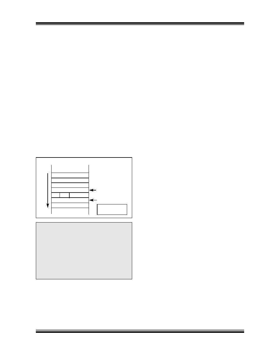
©
2006 Microchip Technology Inc.
Advance Information
DS70178A-page 53
dsPIC30F1010/202X
5.4
Interrupt Sequence
All interrupt event flags are sampled in the beginning of
each instruction cycle by the IFSx registers. A pending
interrupt request (IRQ) is indicated by the flag bit being
equal to a `
1
' in an IFSx register. The IRQ will cause an
interrupt to occur if the corresponding bit in the interrupt
enable (IECx) register is set. For the remainder of the
instruction cycle, the priorities of all pending interrupt
requests are evaluated.
If there is a pending IRQ with a priority level greater
than the current processor priority level in the IPL bits,
the processor will be interrupted.
The processor then stacks the current Program
Counter and the low byte of the processor STATUS
Register (SRL), as shown in Figure 5-2. The low byte
of the STATUS register contains the processor priority
level at the time, prior to the beginning of the interrupt
cycle. The processor then loads the priority level for
this interrupt into the STATUS register. This action will
disable all lower priority interrupts until the completion
of the Interrupt Service Routine (ISR).
FIGURE 5-2:
INTERRUPT STACK
FRAME
The
RETFIE
(Return from Interrupt) instruction will
unstack the Program Counter and status registers to
return the processor to its state prior to the interrupt
sequence.
5.5
Alternate Vector Table
In Program Memory, the IVT is followed by the AIVT, as
shown in Figure 5-1. Access to the Alternate Vector
Table is provided by the ALTIVT bit in the INTCON2
register. If the ALTIVT bit is set, all interrupt and excep-
tion processes will use the alternate vectors instead of
the default vectors. The alternate vectors are organized
in the same manner as the default vectors. The AIVT
supports emulation and debugging efforts by providing
a means to switch between an application and a sup-
port environment, without requiring the interrupt vec-
tors to be reprogrammed. This feature also enables
switching between applications for evaluation of
different software algorithms at run time.
If the AIVT is not required, the program memory allo-
cated to the AIVT may be used for other purposes.
AIVT is not a protected section and may be freely
programmed by the user.
5.6
Fast Context Saving
A context saving option is available using shadow reg-
isters. Shadow registers are provided for the DC, N,
OV, Z and C bits in SR, and the registers W0 through
W3. The shadows are only one level deep. The shadow
registers are accessible using the
PUSH.S
and
POP.S
instructions only.
When the processor vectors to an interrupt, the
PUSH.S
instruction can be used to store the current
value of the aforementioned registers into their
respective shadow registers.
If an ISR of a certain priority uses the
PUSH.S
and
POP.S
instructions for fast context saving, then a
higher priority ISR should not include the same instruc-
tions. Users must save the key registers in software
during a lower priority interrupt, if the higher priority ISR
uses fast context saving.
5.7
External Interrupt Requests
The interrupt controller supports five external interrupt
request signals, INT0-INT4. These inputs are edge
sensitive; they require a low-to-high or a high-to-low
transition to generate an interrupt request. The
INTCON2 register has five bits, INT0EP-INT4EP, that
select the polarity of the edge detection circuitry.
5.8
Wake-up from Sleep and Idle
The interrupt controller may be used to wake-up the
processor from either Sleep or Idle modes, if Sleep or
Idle mode is active when the interrupt is generated.
If an enabled interrupt request of sufficient priority is
received by the interrupt controller, then the standard
interrupt request is presented to the processor. At the
same time, the processor will wake-up from Sleep or
Idle and begin execution of the Interrupt Service
Routine needed to process the interrupt request.
Note 1: The user can always lower the priority
level by writing a new value into SR. The
Interrupt Service Routine must clear the
interrupt flag bits in the IFSx register
before lowering the processor interrupt
priority, in order to avoid recursive
interrupts.
2: The IPL3 bit (CORCON<3>) is always
clear when interrupts are being pro-
cessed. It is set only during execution of
traps.
<Free Word>
0
15
W15 (before
CALL
)
W15 (after
CALL
)
S
t
ack
G
r
ow
s
T
o
w
a
rd
s
H
i
g
her Addre
s
s
PUSH : [W15++]
POP : [--W15]
0x0000
PC<15:0>
SRL IPL3 PC<22:16>

dsPIC30F1010/202X
DS70178A-page 54
Advance Information
©
2006 Microchip Technology Inc.
REGISTER 5-1:
INTCON1: INTERRUPT CONTROL REGISTER 1
R/W-0
R/W-0
R/W-0
R/W-0
R/W-0
R/W-0
R/W-0
R/W-0
NSTDIS
OVAERR
OVBERR
COVAERR
COVBERR
OVATE
OVBTE
COVTE
bit 15
bit 8
R/W-0
R/W-0
U-0
R/W-0
R/W-0
R/W-0
R/W-0
U-0
SFTACERR
DIV0ERR
--
MATHERR
ADDRERR
STKERR
OSCFAIL
--
bit 7
bit 0
Legend:
R = Readable bit
W = Writable bit
U = Unimplemented bit, read as `0'
-n = Value at POR
`1' = Bit is set
`0' = Bit is cleared
x = Bit is unknown
bit 15
NSTDIS: Interrupt Nesting Disable bit
1
= Interrupt nesting is disabled
0
= Interrupt nesting is enabled
bit 14
OVAERR: Accumulator A Overflow Trap Flag bit
1
= Trap was caused by overflow of Accumulator A
0
= Trap was not caused by overflow of Accumulator A
bit 13
OVBERR: Accumulator B Overflow Trap Flag bit
1
= Trap was caused by overflow of Accumulator B
0
= Trap was not caused by overflow of Accumulator B
bit 12
COVAERR: Accumulator A Catastrophic Overflow Trap Enable bit
1
= Trap was caused by catastrophic overflow of Accumulator A
0
= Trap was not caused by catastrophic overflow of Accumulator A
bit 11
COVBERR: Accumulator B Catastrophic Overflow Trap Enable bit
1
= Trap was caused by catastrophic overflow of Accumulator B
0
= Trap was not caused by catastrophic overflow of Accumulator B
bit 10
OVATE: Accumulator A Overflow Trap Enable bit
1
= Trap overflow of Accumulator A
0
= Trap disabled
bit 9
OVBTE: Accumulator B Overflow Trap Enable bit
1
= Trap overflow of Accumulator B
0
= Trap disabled
bit 8
COVTE: Catastrophic Overflow Trap Enable bit
1
= Trap on catastrophic overflow of Accumulator A or B enabled
0
= Trap disabled
bit 7
SFTACERR: Shift Accumulator Error Status bit
1
= Math error trap was caused by an invalid accumulator shift
0
= Math error trap was not caused by an invalid accumulator shift
bit 6
DIV0ERR: Arithmetic Error Status bit
1
= Math error trap was caused by a divided by zero
0
= Math error trap was not caused by an invalid accumulator shift
bit 5
Unimplemented: Read as `
0
'
bit 4
MATHERR: Arithmetic Error Status bit
1
= Overflow trap has occurred
0
= Overflow trap has not occurred
bit 3
ADDRERR: Address Error Trap Status bit
1
= Address error trap has occurred
0
= Address error trap has not occurred

©
2006 Microchip Technology Inc.
Advance Information
DS70178A-page 55
dsPIC30F1010/202X
bit 2
STKERR: Stack Error Trap Status bit
1
= Stack error trap has occurred
0
= Stack error trap has not occurred
bit 1
OSCFAIL: Oscillator Failure Trap Status bit
1
= Oscillator failure trap has occurred
0
= Oscillator failure trap has not occurred
bit 0
Unimplemented: Read as `
0
'
REGISTER 5-1:
INTCON1: INTERRUPT CONTROL REGISTER 1 (CONTINUED)

dsPIC30F1010/202X
DS70178A-page 56
Advance Information
©
2006 Microchip Technology Inc.
REGISTER 5-2:
INTCON2: INTERRUPT CONTROL REGISTER 2
R/W-0
R-0
U-0
U-0
U-0
U-0
U-0
U-0
ALTIVT
DISI
--
--
--
--
--
--
bit 15
bit 8
U-0
U-0
U-0
U-0
U-0
R/W-0
R/W-0
R/W-0
--
--
--
--
--
INT2EP
INT1EP
INT0EP
bit 7
bit 0
Legend:
R = Readable bit
W = Writable bit
U = Unimplemented bit, read as `0'
-n = Value at POR
`1' = Bit is set
`0' = Bit is cleared
x = Bit is unknown
bit 15
ALTIVT: Enable Alternate Interrupt Vector Table bit
1
= Use alternate vector table
0
= Use standard (default) vector table
bit 14
DISI:
DISI
Instruction Status bit
1
=
DISI
instruction is active
0
=
DISI
instruction is not active
bit 13-3
Unimplemented: Read as `
0
'
bit 2
INT2EP: External Interrupt 2 Edge Detect Polarity Select bit
1
= Interrupt on negative edge
0
= Interrupt on positive edge
bit 1
INT1EP: External Interrupt 1 Edge Detect Polarity Select bit
1
= Interrupt on negative edge
0
= Interrupt on positive edge
bit 0
INT0EP: External Interrupt 0 Edge Detect Polarity Select bit
1
= Interrupt on negative edge
0
= Interrupt on positive edge

©
2006 Microchip Technology Inc.
Advance Information
DS70178A-page 57
dsPIC30F1010/202X
REGISTER 5-3:
IFS0: INTERRUPT FLAG STATUS REGISTER 0
U-0
R/W-0
R/W-0
R/W-0
R/W-0
R/W-0
R/W-0
R/W-0
--
MI2CIF
SI2CIF
NVMIF
ADIF
U1TXIF
U1RXIF
SPI1IF
bit 15
bit 8
R/W-0
R/W-0
R/W-0
U-0
R/W-0
R/W-0
R/W-0
R/W-0
T3IF
T2IF
OC2IF
--
T1IF
OC1IF
IC1IF
INT0IF
bit 7
bit 0
Legend:
R = Readable bit
W = Writable bit
U = Unimplemented bit, read as `0'
-n = Value at POR
`1' = Bit is set
`0' = Bit is cleared
x = Bit is unknown
bit 15
Unimplemented: Read as `
0
'
bit 14
MI2CIF: I
2
C Master Events Interrupt Flag Status bit
1
= Interrupt request has occurred
0
= Interrupt request has not occurred
bit 13
SI2CIF: I
2
C Slave Events Interrupt Flag Status bit
1
= Interrupt request has occurred
0
= Interrupt request has not occurred
bit 12
NVMIF: Nonvolatile Memory Interrupt Flag Status bit
1
= Interrupt request has occurred
0
= Interrupt request has not occurred
bit 11
ADIF: ADC Conversion Complete Interrupt Flag Status bit
1
= Interrupt request has occurred
0
= Interrupt request has not occurred
bit 10
U1TXIF: UART1 Transmitter Interrupt Flag Status bit
1
= Interrupt request has occurred
0
= Interrupt request has not occurred
bit 9
U1RXIF: UART1 Receiver Interrupt Flag Status bit
1
= Interrupt request has occurred
0
= Interrupt request has not occurred
bit 8
SPI1IF: SPI1 Event Interrupt Flag Status bit
1
= Interrupt request has occurred
0
= Interrupt request has not occurred
bit 7
T3IF: Timer3 Interrupt Flag Status bit
1
= Interrupt request has occurred
0
= Interrupt request has not occurred
bit 6
T2IF: Timer2 Interrupt Flag Status bit
1
= Interrupt request has occurred
0
= Interrupt request has not occurred
bit 5
OC2IF: Output Compare Channel 2 Interrupt Flag Status bit
1
= Interrupt request has occurred
0
= Interrupt request has not occurred
bit 4
Unimplemented: Read as `
0
'
bit 3
T1IF: Timer1 Interrupt Flag Status bit
1
= Interrupt request has occurred
0
= Interrupt request has not occurred

dsPIC30F1010/202X
DS70178A-page 58
Advance Information
©
2006 Microchip Technology Inc.
bit 2
OC1IF: Output Compare Channel 1 Interrupt Flag Status bit
1
= Interrupt request has occurred
0
= Interrupt request has not occurred
bit 1
IC1IF: Input Capture Channel 1 Interrupt Flag Status bit
1
= Interrupt request has occurred
0
= Interrupt request has not occurred
bit 0
INT0IF: External Interrupt 0 Flag Status bit
1
= Interrupt request has occurred
0
= Interrupt request has not occurred
REGISTER 5-3:
IFS0: INTERRUPT FLAG STATUS REGISTER 0 (CONTINUED)

©
2006 Microchip Technology Inc.
Advance Information
DS70178A-page 59
dsPIC30F1010/202X
REGISTER 5-4:
IFS1: INTERRUPT FLAG STATUS REGISTER 1
R/W-0
R/W-0
R/W-0
U-0
R/W-0
U-0
U-0
U-0
AC3IF
AC2IF
AC1IF
--
CNIF
--
--
--
bit 15
bit 8
U-0
R/W-0
R/W-0
R/W-0
R/W-0
R/W-0
R/W-0
R/W-0
--
PWM4IF
PWM3IF
PWM2IF
PWM1IF
PSEMIF
INT2IF
INT1IF
bit 7
bit 0
Legend:
R = Readable bit
W = Writable bit
U = Unimplemented bit, read as `0'
-n = Value at POR
`1' = Bit is set
`0' = Bit is cleared
x = Bit is unknown
bit 15
AC3IF: Analog Comparator #3 Interrupt Flag Status bit
1
= Interrupt request has occurred
0
= Interrupt request has not occurred
bit 14
AC2IF: Analog Comparator #2 Interrupt Flag Status bit
1
= Interrupt request has occurred
0
= Interrupt request has not occurred
bit 13
AC1IF: Analog Comparator #1 Interrupt Flag Status bit
1
= Interrupt request has occurred
0
= Interrupt request has not occurred
bit 12
Unimplemented: Read as `
0
'
bit 11
CNIF: Input Change Notification Interrupt Flag Status bit
1 = Interrupt request has occurred
0 = Interrupt request has not occurred
bit 10 -7
Unimplemented: Read as `
0
'
bit 6
PWM4IF: Pulse Width Modulation Generator #4 Interrupt Flag Status bit
1
= Interrupt request has occurred
0
= Interrupt request has not occurred
bit 5
PWM3IF: Pulse Width Modulation Generator #3 Interrupt Flag Status bit
1
= Interrupt request has occurred
0
= Interrupt request has not occurred
bit 4
PWM2IF: Pulse Width Modulation Generator #2 Interrupt Flag Status bit
1
= Interrupt request has occurred
0
= Interrupt request has not occurred
bit 3
PWM1IF: Pulse Width Modulation Generator #1 Interrupt Flag Status bit
1
= Interrupt request has occurred
0
= Interrupt request has not occurred
bit 2
PSEMIF: PWM Special Event Match Interrupt Flag Status bit
1
= Interrupt request has occurred
0
= Interrupt request has not occurred
bit 1
INT2IF: External Interrupt 2 Flag Status bit
1
= Interrupt request has occurred
0
= Interrupt request has not occurred
bit 0
INT1IF: External Interrupt 1 Flag Status bit
1
= Interrupt request has occurred
0
= Interrupt request has not occurred

dsPIC30F1010/202X
DS70178A-page 60
Advance Information
©
2006 Microchip Technology Inc.
REGISTER 5-5:
IFS2: INTERRUPT FLAG STATUS REGISTER 2
U-0
U-0
U-0
U-0
U-0
R/W-0
R/W-00
R/W-0
--
--
--
--
--
ADCP5IF
ADCP4IF
ADCP3IF
bit 15
bit 8
R/W-0
R/W-0
R/W-0
U-0
U-0
U-0
U-0
R/W-0
ADCP2IF
ADCP1IF
ADCP0IF
--
--
--
--
AC4IF
bit 7
bit 0
Legend:
R = Readable bit
W = Writable bit
U = Unimplemented bit, read as `0'
-n = Value at POR
`1' = Bit is set
`0' = Bit is cleared
x = Bit is unknown
bit 15-11
Unimplemented: Read as `
0
'
bit 10
ADCP5IF: ADC Pair 5 Conversion Done Interrupt Flag Status bit
1
= Interrupt request has occurred
0
= Interrupt request has not occurred
bit 9
ADCP4IF: ADC Pair 4 Conversion Done Interrupt Flag Status bit
1
= Interrupt request has occurred
0
= Interrupt request has not occurred
bit 8
ADCP3IF: ADC Pair 3 Conversion Done Interrupt Flag Status bit
1
= Interrupt request has occurred
0
= Interrupt request has not occurred
bit 7
ADCP2IF: ADC Pair 2 Conversion Done Interrupt Flag Status bit
1
= Interrupt request has occurred
0
= Interrupt request has not occurred
bit 6
ADCP1IF: ADC Pair 1 Conversion Done Interrupt Flag Status bit
1
= Interrupt request has occurred
0
= Interrupt request has not occurred
bit 5
ADCP0IF: ADC Pair 0 Conversion Done Interrupt Flag Status bit
1
= Interrupt request has occurred
0
= Interrupt request has not occurred
bit 4-1
Unimplemented: Read as `
0
'
bit 0
AC4IF: Analog Comparator #4 Interrupt Flag Status bit
1
= Interrupt request has occurred
0
= Interrupt request has not occurred

©
2006 Microchip Technology Inc.
Advance Information
DS70178A-page 61
dsPIC30F1010/202X
REGISTER 5-6:
IEC0: INTERRUPT ENABLE CONTROL REGISTER 0
U-0
R/W-0
R/W-0
R/W-0
R/W-0
R/W-0
R/W-0
R/W-0
--
MI2CIE
SI2CIE
NVMIE
ADIE
U1TXIE
U1RXIE
SPI1IE
bit 15
bit 8
R/W-0
R/W-0
R/W-0
U-0
R/W-0
R/W-0
R/W-0
R/W-0
T3IE
T2IE
OC2IE
--
T1IE
OC1IE
IC1IE
INT0IE
bit 7
bit 0
Legend:
R = Readable bit
W = Writable bit
U = Unimplemented bit, read as `0'
-n = Value at POR
`1' = Bit is set
`0' = Bit is cleared
x = Bit is unknown
bit 15
Unimplemented: Read as `
0
'
bit 14
MI2CIE: I
2
C Master Events Interrupt Enable bit
1
= Interrupt request enabled
0
= Interrupt request not enabled
bit 13
SI2CIE: I
2
C Slave Events Interrupt Enable bit
1
= Interrupt request enabled
0
= Interrupt request not enabled
bit 12
NVMIE: Nonvolatile Memory Interrupt Enable bit
1
= Interrupt request enabled
0
= Interrupt request not enabled
bit 11
ADIE: ADC Conversion Complete Interrupt Enable bit
1
= Interrupt request enabled
0
= Interrupt request not enabled
bit 10
U1TXIE: UART1 Transmitter Interrupt Enable bit
1
= Interrupt request enabled
0
= Interrupt request not enabled
bit 9
U1RXIE: UART1 Receiver Interrupt Enable bit
1
= Interrupt request enabled
0
= Interrupt request not enabled
bit 8
SPI1IE: SPI1 Event Interrupt Enable bit
1
= Interrupt request enabled
0
= Interrupt request not enabled
bit 7
T3IE: Timer3 Interrupt Enable bit
1
= Interrupt request enabled
0
= Interrupt request not enabled
bit 6
T2IE: Timer2 Interrupt Enable bit
1
= Interrupt request enabled
0
= Interrupt request not enabled
bit 5
OC2IE: Output Compare Channel 2 Interrupt Enable bit
1
= Interrupt request enabled
0
= Interrupt request not enabled
bit 4
Unimplemented: Read as `
0
'
bit 3
T1IE: Timer1 Interrupt Enable bit
1
= Interrupt request enabled
0
= Interrupt request not enabled

dsPIC30F1010/202X
DS70178A-page 62
Advance Information
©
2006 Microchip Technology Inc.
bit 2
OC1IE: Output Compare Channel 1 Interrupt Enable bit
1
= Interrupt request enabled
0
= Interrupt request not enabled
bit 1
IC1IE: Input Capture Channel 1 Interrupt Enable bit
1
= Interrupt request enabled
0
= Interrupt request not enabled
bit 0
INT0IE: External Interrupt 0 Enable bit
1
= Interrupt request enabled
0
= Interrupt request not enabled
REGISTER 5-6:
IEC0: INTERRUPT ENABLE CONTROL REGISTER 0 (CONTINUED)

©
2006 Microchip Technology Inc.
Advance Information
DS70178A-page 63
dsPIC30F1010/202X
REGISTER 5-7:
IEC1: INTERRUPT ENABLE CONTROL REGISTER 1
R/W-0
R/W-0
R/W-0
U-0
R/W-0
U-0
U-0
U-0
AC3IE
AC2IE
AC1IE
--
CNIE
--
--
--
bit 15
bit 8
U-0
R/W-0
R/W-0
R/W-0
R/W-0
R/W-0
R/W-0
R/W-0
--
PWM4IE
PWM3IE
PWM2IE
PWM1IE
PSEMIE
INT2IE
INT1IE
bit 7
bit 0
Legend:
R = Readable bit
W = Writable bit
U = Unimplemented bit, read as `0'
-n = Value at POR
`1' = Bit is set
`0' = Bit is cleared
x = Bit is unknown
bit 15
AC3IE: Analog Comparator #3 Interrupt Enable bit
1
= Interrupt request enabled
0
= Interrupt request not enabled
bit 14
AC2IE: Analog Comparator #2 Interrupt Enable bit
1
= Interrupt request enabled
0
= Interrupt request not enabled
bit 13
AC1IE: Analog Comparator #1 Interrupt Enable bit
1
= Interrupt request enabled
0
= Interrupt request not enabled
bit 12
Unimplemented: Read as `
0
'
bit 11
CNIE: Input Change Notification Interrupt Enable bit
1
= Interrupt request enabled
0
= Interrupt request not enabled
bit 10 -7
Unimplemented: Read as `
0
'
bit 6
PWM4IE: Pulse Width Modulation Generator #4 Interrupt Enable bit
1
= Interrupt request enabled
0
= Interrupt request not enabled
bit 5
PWM3IE: Pulse Width Modulation Generator #3 Interrupt Enable bit
1
= Interrupt request enabled
0
= Interrupt request not enabled
bit 4
PWM2IE: Pulse Width Modulation Generator #2 Interrupt Enable bit
1
= Interrupt request enabled
0
= Interrupt request not enabled
bit 3
PWM1IE: Pulse Width Modulation Generator #1 Interrupt Enable bit
1
= Interrupt request enabled
0
= Interrupt request not enabled
bit 2
PSEMIE: PWM Special Event Match Interrupt Enable bit
1
= Interrupt request enabled
0
= Interrupt request not enabled
bit 1
INT2IE: External Interrupt 2 Enable bit
1
= Interrupt request enabled
0
= Interrupt request not enabled
bit 0
INT1IE: External Interrupt 1 Enable bit
1
= Interrupt request enabled
0
= Interrupt request not enabled

dsPIC30F1010/202X
DS70178A-page 64
Advance Information
©
2006 Microchip Technology Inc.
REGISTER 5-8:
IEC2: INTERRUPT ENABLE CONTROL REGISTER 2
U-0
U-0
U-0
U-0
U-0
R/W-0
R/W-0
R/W-0
--
--
--
--
--
ADCP5IE
ADCP4IE
ADCP3IE
bit 15
bit 8
R/W-0
R/W-0
R/W-0
U-0
U-0
U-0
U-0
R/W-0
ADCP2IE
ADCP1IE
ADCP0IE
--
--
--
--
AC4IE
bit 7
bit 0
Legend:
R = Readable bit
W = Writable bit
U = Unimplemented bit, read as `0'
-n = Value at POR
`1' = Bit is set
`0' = Bit is cleared
x = Bit is unknown
bit 15 -11
Unimplemented: Read as `
0
'
bit 10
ADCP5IE: ADC Pair 5 Conversion done Interrupt Enable bit
1
= Interrupt request enabled
0
= Interrupt request not enabled
bit 9
ADCP5IE: ADC Pair 5 Conversion done Interrupt Enable bit
1
= Interrupt request enabled
0
= Interrupt request not enabled
bit 8
ADCP4IE: ADC Pair 4 Conversion done Interrupt Enable bit
1
= Interrupt request enabled
0
= Interrupt request not enabled
bit 7
ADCP3IE: ADC Pair 3 Conversion done Interrupt Enable bit
1
= Interrupt request enabled
0
= Interrupt request not enabled
bit 8
ADCP2IE: ADC Pair 2 Conversion done Interrupt Enable bit
1
= Interrupt request enabled
0
= Interrupt request not enabled
bit 7
ADCP1IE: ADC Pair 1 Conversion done Interrupt Enable bit
1
= Interrupt request enabled
0
= Interrupt request not enabled
bit 6
ADCP0IE: ADC Pair 0 Conversion done Interrupt Enable bit
1
= Interrupt request enabled
0
= Interrupt request not enabled
bit 4 -1
Unimplemented: Read as `
0
'
bit 0
AC4IE: Analog Comparator #4 Interrupt Enable bit
1
= Interrupt request enabled
0
= Interrupt request not enabled

©
2006 Microchip Technology Inc.
Advance Information
DS70178A-page 65
dsPIC30F1010/202X
REGISTER 5-9:
IPC0: INTERRUPT PRIORITY CONTROL REGISTER 0
U-0
R/W-1
R/W-0
R/W-0
U-0
R/W-1
R/W-0
R/W-0
--
T1IP<2:0>
--
OC1IP<2:0>
bit 15
bit 8
U-0
R/W-1
R/W-0
R/W-0
U-0
R/W-1
R/W-0
R/W-0
--
IC1IP<2:0>
--
INT0IP<2:0>
bit 7
bit 0
Legend:
R = Readable bit
W = Writable bit
U = Unimplemented bit, read as `0'
-n = Value at POR
`1' = Bit is set
`0' = Bit is cleared
x = Bit is unknown
bit 15
Unimplemented: Read as `
0
'
bit 14-12
T1IP<2:0>: Timer1 Interrupt Priority bits
111
= Interrupt is priority 7 (highest priority interrupt)
∑
∑
∑
001
= Interrupt is priority 1
000
= Interrupt source is disabled
bit 11
Unimplemented: Read as `
0
'
bit 10-8
OC1IP<2:0>: Output Compare Channel 1 Interrupt Priority bits
111
= Interrupt is priority 7 (highest priority interrupt)
∑
∑
∑
001
= Interrupt is priority 1
000
= Interrupt source is disabled
bit 7
Unimplemented: Read as `
0
'
bit 6-4
IC1IP<2:0>: Input Capture Channel 1 Interrupt Priority bits
111
= Interrupt is priority 7 (highest priority interrupt)
∑
∑
∑
001
= Interrupt is priority 1
000
= Interrupt source is disabled
bit 3
Unimplemented: Read as `
0
'
bit 2-0
INT0IP<2:0>: External Interrupt 0 Priority bits
111
= Interrupt is priority 7 (highest priority interrupt)
∑
∑
∑
001
= Interrupt is priority 1
000
= Interrupt source is disabled

dsPIC30F1010/202X
DS70178A-page 66
Advance Information
©
2006 Microchip Technology Inc.
REGISTER 5-10:
IPC1: INTERRUPT PRIORITY CONTROL REGISTER 1
U-0
R/W-1
R/W-0
R/W-0
U-0
R/W-1
R/W-0
R/W-0
--
T3IP<2:0>
--
T2IP<2:0>
bit 15
bit 8
U-0
R/W-1
R/W-0
R/W-0
U-0
U-0
U-0
U-0
--
OC2IP<2:0>
--
--
--
--
bit 7
bit 0
Legend:
R = Readable bit
W = Writable bit
U = Unimplemented bit, read as `0'
-n = Value at POR
`1' = Bit is set
`0' = Bit is cleared
x = Bit is unknown
bit 15
Unimplemented: Read as `
0
'
bit 14-12
T3IP<2:0>: Timer3 Interrupt Priority bits
111
= Interrupt is priority 7 (highest priority interrupt)
∑
∑
∑
001
= Interrupt is priority 1
000
= Interrupt source is disabled
bit 11
Unimplemented: Read as `
0
'
bit 10-8
T2IP<2:0>: Timer2 Interrupt Priority bits
111
= Interrupt is priority 7 (highest priority interrupt)
∑
∑
∑
001
= Interrupt is priority 1
000
= Interrupt source is disabled
bit 7
Unimplemented: Read as `
0
'
bit 6-4
OC2IP<2:0>: Output Compare Channel 2 Interrupt Priority bits
111
= Interrupt is priority 7 (highest priority interrupt)
∑
∑
∑
001
= Interrupt is priority 1
000
= Interrupt source is disabled
bit 3-0
Unimplemented: Read as `
0
'

©
2006 Microchip Technology Inc.
Advance Information
DS70178A-page 67
dsPIC30F1010/202X
REGISTER 5-11:
IPC2: INTERRUPT PRIORITY CONTROL REGISTER 2
U-0
R/W-1
R/W-0
R/W-0
U-0
R/W-1
R/W-0
R/W-0
--
ADIP<2:0>
--
U1TXIP<2:0>
bit 15
bit 8
U-0
R/W-1
R/W-0
R/W-0
U-0
R/W-1
R/W-0
R/W-0
--
U1RXIP<2:0>
--
SPI1IP<2:0>
bit 7
bit 0
Legend:
R = Readable bit
W = Writable bit
U = Unimplemented bit, read as `0'
-n = Value at POR
`1' = Bit is set
`0' = Bit is cleared
x = Bit is unknown
bit 15
Unimplemented: Read as `
0
'
bit 14-12
ADIP<2:0>: ADC Conversion Complete Interrupt Priority bits
111
= Interrupt is priority 7 (highest priority interrupt)
∑
∑
∑
001
= Interrupt is priority 1
000
= Interrupt source is disabled
bit 11
Unimplemented: Read as `
0
'
bit 10-8
U1TXIP<2:0>: UART1 Transmitter Interrupt Priority bits
111
= Interrupt is priority 7 (highest priority interrupt)
∑
∑
∑
001
= Interrupt is priority 1
000
= Interrupt source is disabled
bit 7
Unimplemented: Read as `
0
'
bit 6-4
U1RXIP<2:0>: UART1 Receiver Interrupt Priority bits
111
= Interrupt is priority 7 (highest priority interrupt)
∑
∑
∑
001
= Interrupt is priority 1
000
= Interrupt source is disabled
bit 3
Unimplemented: Read as `
0
'
bit 2-0
SPI1IP<2:0>: SPI1 Event Interrupt Priority bits
111
= Interrupt is priority 7 (highest priority interrupt)
∑
∑
∑
001
= Interrupt is priority 1
000
= Interrupt source is disabled

dsPIC30F1010/202X
DS70178A-page 68
Advance Information
©
2006 Microchip Technology Inc.
REGISTER 5-12:
IPC3: INTERRUPT CONTROL REGISTER 3
U-0
U-0
U-0
U-0
U-0
R/W-1
R/W-0
R/W-0
--
--
--
--
--
MI2CIP<2:0>
bit 15
bit 8
U-0
R/W-1
R/W-0
R/W-0
U-0
R/W-1
R/W-0
R/W-0
--
SI2CIP<2:0>
--
NVMIP<2:0>
bit 7
bit 0
Legend:
R = Readable bit
W = Writable bit
U = Unimplemented bit, read as `0'
-n = Value at POR
`1' = Bit is set
`0' = Bit is cleared
x = Bit is unknown
bit 15-11
Unimplemented: Read as `
0
'
bit 10-8
MI2CIP<2:0>: I
2
C Master Events Interrupt Priority bits
111
= Interrupt is priority 7 (highest priority interrupt)
∑
∑
∑
001
= Interrupt is priority 1
000
= Interrupt source is disabled
bit 7
Unimplemented: Read as `
0
'
bit 6-4
SI2CIP<2:0>: I
2
C Slave Events Interrupt Priority bits
111
= Interrupt is priority 7 (highest priority interrupt)
∑
∑
∑
001
= Interrupt is priority 1
000
= Interrupt source is disabled
bit 3
Unimplemented: Read as `
0
'
bit 2-0
NVMIP<2:0>: Nonvolatile Memory Interrupt Priority bits
111
= Interrupt is priority 7 (highest priority interrupt)
∑
∑
∑
001
= Interrupt is priority 1
000
= Interrupt source is disabled

©
2006 Microchip Technology Inc.
Advance Information
DS70178A-page 69
dsPIC30F1010/202X
REGISTER 5-13:
IPC4: INTERRUPT PRIORITY CONTROL REGISTER 4
U-0
R/W-1
R/W-0
R/W-0
U-0
R/W-1
R/W-0
R/W-0
--
PWM1IP<2:0>
--
PSEMIP<2:0>
bit 15
bit 8
U-0
R/W-1
R/W-0
R/W-0
U-0
R/W-1
R/W-0
R/W-0
--
INT2IP<2:0>
--
INT1IP<2:0>
bit 7
bit 0
Legend:
R = Readable bit
W = Writable bit
U = Unimplemented bit, read as `0'
-n = Value at POR
`1' = Bit is set
`0' = Bit is cleared
x = Bit is unknown
bit 15
Unimplemented: Read as `
0
'
bit 14-12
PWM1IP<2:0>: PWM Generator #1 Interrupt Priority bits
111
= Interrupt is priority 7 (highest priority interrupt)
∑
∑
∑
001
= Interrupt is priority 1
000
= Interrupt source is disabled
bit 11
Unimplemented: Read as `
0
'
bit 10-8
PSEMIP<2:0>: PWM Special Event Match Priority bits
111
= Interrupt is priority 7 (highest priority interrupt)
∑
∑
∑
001
= Interrupt is priority 1
000
= Interrupt source is disabled
bit 7
Unimplemented: Read as `
0
'
bit 6-4
INT2IP<2:0>: External Interrupt 2 Priority bits
111
= Interrupt is priority 7 (highest priority interrupt)
∑
∑
∑
001
= Interrupt is priority 1
000
= Interrupt source is disabled
bit 3
Unimplemented: Read as `
0
'
bit 2-0
INT1IP<2:0>: External Interrupt 1 Priority bits
111
= Interrupt is priority 7 (highest priority interrupt)
∑
∑
∑
001
= Interrupt is priority 1
000
= Interrupt source is disabled

dsPIC30F1010/202X
DS70178A-page 70
Advance Information
©
2006 Microchip Technology Inc.
REGISTER 5-14:
IPC5: INTERRUPT PRIORITY CONTROL REGISTER 5
U-0
U-0
U-0
U-0
U-0
R/W-1
R/W-0
R/W-0
--
--
--
--
--
PWM4IP<2:0>
bit 15
bit 8
U-0
R/W-1
R/W-0
R/W-0
U-0
R/W-1
R/W-0
R/W-0
--
PWM3IP<2:0>
--
PWM2IP<2:0>
bit 7
bit 0
Legend:
R = Readable bit
W = Writable bit
U = Unimplemented bit, read as `0'
-n = Value at POR
`1' = Bit is set
`0' = Bit is cleared
x = Bit is unknown
bit 15-11
Unimplemented: Read as `
0
'
bit 10-8
PWM4IP<2:0>: PWM Generator #4 Interrupt Priority bits
111
= Interrupt is priority 7 (highest priority interrupt)
∑
∑
∑
001
= Interrupt is priority 1
000
= Interrupt source is disabled
bit 7
Unimplemented: Read as `
0
'
bit 6-4
PWM3IP<2:0>: PWM Generator #3 Interrupt Priority bits
111
= Interrupt is priority 7 (highest priority interrupt)
∑
∑
∑
001
= Interrupt is priority 1
000
= Interrupt source is disabled
bit 3
Unimplemented: Read as `
0
'
bit 2-0
PWM2IP<2:0>: PWM Generator #2 Interrupt Priority bits
111
= Interrupt is priority 7 (highest priority interrupt)
∑
∑
∑
001
= Interrupt is priority 1
000
= Interrupt source is disabled

©
2006 Microchip Technology Inc.
Advance Information
DS70178A-page 71
dsPIC30F1010/202X
REGISTER 5-15:
IPC6: INTERRUPT PRIORITY CONTROL REGISTER 6
U-0
R/W-1
R/W-0
R/W-0
U-0
U-0
U-0
U-0
--
CNIP<2:0>
--
--
--
--
bit 15
bit 8
U-0
U-0
U-0
U-0
U-0
U-0
U-0
U-0
--
--
--
--
--
--
--
--
bit 7
bit 0
Legend:
R = Readable bit
W = Writable bit
U = Unimplemented bit, read as `0'
-n = Value at POR
`1' = Bit is set
`0' = Bit is cleared
x = Bit is unknown
bit 15
Unimplemented: Read as `
0
'
bit 14-12
CNIP<2:0>: Change Notification Interrupt Priority bits
111
= Interrupt is priority 7 (highest priority interrupt)
∑
∑
∑
001
= Interrupt is priority 1
000
= Interrupt source is disabled
bit 11-0
Unimplemented: Read as `
0
'

dsPIC30F1010/202X
DS70178A-page 72
Advance Information
©
2006 Microchip Technology Inc.
REGISTER 5-16:
IPC7: INTERRUPT PRIORITY CONTROL REGISTER 7
U-0
R/W-1
R/W-0
R/W-0
U-0
R/W-1
R/W-0
R/W-0
--
AC3IP<2:0>
--
AC2IP<2:0>
bit 15
bit 8
U-0
R/W-1
R/W-0
R/W-0
U-0
U-0
U-0
U-0
--
AC1IP<2:0>
--
--
--
--
bit 7
bit 0
Legend:
R = Readable bit
W = Writable bit
U = Unimplemented bit, read as `0'
-n = Value at POR
`1' = Bit is set
`0' = Bit is cleared
x = Bit is unknown
bit 15
Unimplemented: Read as `
0
'
bit 14-12
AC3IP<2:0>: Analog Comparator 3 Interrupt Priority bits
111
= Interrupt is priority 7 (highest priority interrupt)
∑
∑
∑
001
= Interrupt is priority 1
000
= Interrupt source is disabled
bit 11
Unimplemented: Read as `
0
'
bit 10-8
AC2IP<2:0>: Analog Comparator 2 Interrupt Priority bits
111
= Interrupt is priority 7 (highest priority interrupt)
∑
∑
∑
001
= Interrupt is priority 1
000
= Interrupt source is disabled
bit 7
Unimplemented: Read as `
0
'
bit 6-4
AC1IP<2:0>: Analog Comparator 1 Interrupt Priority bits
111
= Interrupt is priority 7 (highest priority interrupt)
∑
∑
∑
001
= Interrupt is priority 1
000
= Interrupt source is disabled
bit 3-0
Unimplemented: Read as `
0
'

©
2006 Microchip Technology Inc.
Advance Information
DS70178A-page 73
dsPIC30F1010/202X
REGISTER 5-17:
IPC8: INTERRUPT PRIORITY CONTROL REGISTER 8
U-0
U-0
U-0
U-0
U-0
U-0
U-0
U-0
--
--
--
--
--
--
--
--
bit 15
bit 8
U-0
U-0
U-0
U-0
U-0
R/W-1
R/W-0
R/W-0
--
--
--
--
--
AC4IP<2:0>
bit 7
bit 0
Legend:
R = Readable bit
W = Writable bit
U = Unimplemented bit, read as `0'
-n = Value at POR
`1' = Bit is set
`0' = Bit is cleared
x = Bit is unknown
bit 15-3
Unimplemented: Read as `
0
'
bit 2-0
AC4IP<2:0>: Analog Comparator 4 Interrupt Priority bits
111
= Interrupt is priority 7 (highest priority interrupt)
∑
∑
∑
001
= Interrupt is priority 1
000
= Interrupt source is disabled

dsPIC30F1010/202X
DS70178A-page 74
Advance Information
©
2006 Microchip Technology Inc.
REGISTER 5-18:
IPC9: INTERRUPT PRIORITY CONTROL REGISTER 9
U-0
R/W-1
R/W-0
R/W-0
U-0
R/W-1
R/W-0
R/W-0
--
ADCP2IP<2:0>
--
ADCP1IP<2:0>
bit 15
bit 8
U-0
R/W-1
R/W-0
R/W-0
U-0
U-0
U-0
U-0
--
ADCP0IP<2:0>
--
--
--
--
bit 7
bit 0
Legend:
R = Readable bit
W = Writable bit
U = Unimplemented bit, read as `0'
-n = Value at POR
`1' = Bit is set
`0' = Bit is cleared
x = Bit is unknown
bit 15
Unimplemented: Read as `
0
'
bit 14 - 12
ADCP2IP<2:0>: ADC Pair 2 Conversion Done Interrupt Priority bits
111
= Interrupt is priority 7 (highest priority interrupt)
∑
∑
∑
001
= Interrupt is priority 1
000
= Interrupt source is disabled
bit 11
Unimplemented: Read as `
0
'
bit 10 - 8
ADCP1IP<2:0>: ADC Pair 1 Conversion Done Interrupt Priority bits
111
= Interrupt is priority 7 (highest priority interrupt)
∑
∑
∑
001
= Interrupt is priority 1
000
= Interrupt source is disabled
bit 7
Unimplemented: Read as `
0
'
bit 6 - 4
ADCP0IP<2:0>: ADC Pair 0 Conversion Done Interrupt Priority bits
111
= Interrupt is priority 7 (highest priority interrupt)
∑
∑
∑
001
= Interrupt is priority 1
000
= Interrupt source is disabled
bit 3 - 0
Unimplemented: Read as `
0
'

©
2006 Microchip Technology Inc.
Advance Information
DS70178A-page 75
dsPIC30F1010/202X
REGISTER 5-19:
IPC10: INTERRUPT PRIORITY CONTROL REGISTER 10
U-0
U-0
U-0
U-0
U-0
R/W-1
R/W-0
R/W-0
--
--
--
--
--
ADCP5IP<2:0>
bit 15
bit 8
U-0
R/W-1
R/W-0
R/W-0
U-0
R/W-1
R/W-0
R/W-0
--
ADCP4IP<2:0>
--
ADCP3IP<2:0>
bit 7
bit 0
Legend:
R = Readable bit
W = Writable bit
U = Unimplemented bit, read as `0'
-n = Value at POR
`1' = Bit is set
`0' = Bit is cleared
x = Bit is unknown
bit 15 -10
Unimplemented: Read as `
0
'
bit 10 - 8
ADCP5IP<2:0>: ADC Pair 5 Conversion Done Interrupt Priority bits
111
= Interrupt is priority 7 (highest priority interrupt)
∑
∑
∑
001
= Interrupt is priority 1
000
= Interrupt source is disabled
bit 7
Unimplemented: Read as `
0
'
bit 10 - 8
ADCP4IP<2:0>: ADC Pair 4 Conversion Done Interrupt Priority bits
111
= Interrupt is priority 7 (highest priority interrupt)
∑
∑
∑
001
= Interrupt is priority 1
000
= Interrupt source is disabled
bit 3
Unimplemented: Read as `
0
'
bit 2 - 0
ADCP3IP<2:0>: ADC Pair 3 Conversion Done Interrupt Priority bits
111
= Interrupt is priority 7 (highest priority interrupt)
∑
∑
∑
001
= Interrupt is priority 1
000
= Interrupt source is disabled

©
2006 Microchip Technology Inc.
Advance Information
DS70178A-page 76
dsPIC30F1010/202X
T
ABLE
5-2:
INTE
RR
UP
T CONTROLLE
R
RE
GIS
T
E
R
MAP
SFR
Na
m
e
ADR
Bi
t 15
Bit
14
Bit 1
3
Bit
12
Bit 1
1
Bi
t 1
0
Bit
9
B
it 8
B
it 7
B
it
6
B
i
t
5
B
it
4
B
it
3
B
it
2
B
it 1
B
it
0
R
es
et
S
t
a
t
e
IN
T
C
O
N
1
008
0
NS
T
D
I
S
O
V
A
E
RR
O
V
BERR
C
O
V
A
E
RR
CO
VBE
RR
O
V
A
T
E
O
V
B
TE
CO
VTE
S
F
T
ACERR
D
I
V
0
E
RR
--M
A
T
H
E
R
R
A
DDRE
R
R
ST
KERR
O
SC
F
A
I
L
--
0000 0000 0000 0000
IN
T
C
O
N
2
008
2
AL
T
I
VT
DI
SI
--
--
--
--
--
--
--
--
--
--
--
I
N
T
2E
P
I
N
T
1E
P
I
N
T
0E
P
0000 0000 0000 0000
IF
S
0
008
4
--
M
I2CIF
S
I2CIF
N
V
M
I
F
A
D
IF
U
1
T
X
IF
U1RX
I
F
S
P
I1IF
T
3
IF
T
2
IF
OC2IF
--
T
1IF
O
C1IF
IC1
I
F
I
N
T
0IF
0000 0000 0000 0000
IF
S
1
008
6
AC3
I
F
A
C2
I
F
AC
1
I
F
--
CNIF
--
--
--
--
P
W
M
4IF
P
W
M
3IF
P
W
M
2IF
P
W
M
1IF
P
S
E
MIF
I
N
T
2IF
I
N
T
1IF
0000 0000 0000 0000
IF
S
2
008
8
--
--
--
--
--
A
D
C
P5
IF
ADCP4
I
F
A
DCP3
I
F
A
DCP2
I
F
A
DCP
4
1
F
A
DCP
0
I
F
--
--
--
--A
C
4
I
F
0000 0000 0000 0000
IE
C
0
009
4
--
M
I2
CIE
S
I2CIE
N
V
M
IE
A
D
IE
U1
T
X
IE
U1RX
IE
S
P
I1
IE
T
3
IE
T
2
IE
O
C
2IE
--
T
1IE
O
C1IE
IC1IE
I
NT
0
I
E
0000 0000 0000 0000
IE
C
1
009
6
A
C
3I
E
A
C
2
IE
A
C
1IE
--
CNIE
--
--
--
--
P
WM
4
I
E
P
WM
3
I
E
P
WM
2
I
E
P
WM
1
I
E
PSE
M
I
E
I
NT
2
I
E
I
NT
1
I
E
0000 0000 0000 0000
IE
C
2
009
8
--
--
--
--
--
A
DCP
5
I
E
A
D
C
P4
IE
ADCP
3
I
E
A
DCP
2
I
E
A
DCP1
I
E
A
DCP0
I
E
--
--
--
--A
C
4
I
E
0000 0000 0000 0000
IP
C
0
00
A
4
--
T
1
I
P
<
2:
0>
--
O
C1IP
<
2
:0>
--
I
C1IP
<
2
:0>
--
I
N
T
0IP
<
2:0>
0100 0100 0100 0100
IP
C
1
00
A
6
--
T
31
P
<
2:
0
>
--
T
2IP
<
2:0>
--
O
C2
IP
<
2
:0
>
--
--
--
--
0100 0100 0100 0000
IP
C
2
00
A
8
--
A
D
I
P
<
2:0>
--
U
1
T
X
I
P
<
2:0>
--
U
1
R
X
I
P
<
2:0>
--
S
P
I
1IP
<
2:0>
0100 0100 0100 0100
IP
C
3
00
A
A
--
--
--
--
--M
I
2
C
I
P
<
2
:
0
>
--
S
I2C
I
P
<
2:0>
--
N
V
M
IP
<
2
:0>
0000 0100 0100 0100
IP
C
4
00A
C
--
P
W
M
1IP
<
2
:
0>
--P
S
E
M
I
P
<
2
:
0
>
--
I
N
T
2IP
<
2
:
0>
--
I
N
T
1IP
<
2:0>
0100 0100 0100 0100
IP
C
5
00
A
E
--
--
--
--
--
P
W
M
4IP
<
2:0>
--
P
W
M
3IP
<
2:0>
--
P
W
M
2IP
<
2:0
>
0000 0100 0100 0100
IP
C
6
00
B
0
--
CNIP<
2
:
0
>
--
--
--
--
--
--
--
--
--
--
--
--
0100 0000 0000 0000
IP
C
7
00
B
2
--
A
C3IP
<
2
:0>
--A
C
2
I
P
<
2
:
0
>
--
A
C1IP
<
2
:0>
--
--
--
--
0100 0100 0100 0000
IP
C
8
00
B
4
--
--
--
--
--
--
--
--
--
--
--
--
--
A
C4IP
<
2
:0>
0000 0000 0000 0100
IP
C
9
00
B
6
--
A
D
C
P
2I
P
<
2
:
0>
--
A
D
C
P
1IP
<
2
:
0>
--
A
D
C
P
0I
P
<
2
:
0>
--
--
--
--
0100 0100 0100 0000
IP
C
1
0
00
B
8
--
--
--
--
--
A
D
C
P
5IP
<
2
:
0>
--
A
D
C
P
4I
P
<
2
:
0>
--
A
D
C
P
3IP
<
2:0>
0000 0100 0100 0100
No
t
e
:
R
e
fer
to th
e "
d
s
PI
C
3
0F
Fam
i
l
y
R
e
feren
c
e
M
anu
al
"
(D
S700
46)
for d
e
s
c
ri
pti
ons
of
regi
st
er b
i
t fi
el
ds.

©
2006 Microchip Technology Inc.
Advance Information
DS70178A-page 77
dsPIC30F1010/202X
6.0
I/O PORTS
All of the device pins (except V
DD
, V
SS
, MCLR and
OSC1/CLKI) are shared between the peripherals and
the parallel I/O ports.
All I/O input ports feature Schmitt Trigger inputs for
improved noise immunity.
6.1
Parallel I/O (PIO) Ports
When a peripheral is enabled and the peripheral is
actively driving an associated pin, the use of the pin as
a general purpose output pin is disabled. The I/O pin
may be read, but the output driver for the parallel port
bit will be disabled. If a peripheral is enabled, but the
peripheral is not actively driving a pin, that pin may be
driven by a port.
All port pins have three registers directly associated
with the operation of the port pin. The data direction
register (TRISx) determines whether the pin is an input
or an output. If the data direction bit is a `
1
', then the pin
is an input. All port pins are defined as inputs after a
Reset. Reads from the latch (LATx), read the latch.
Writes to the latch, write the latch (LATx). Reads from
the port (PORTx), read the port pins, and writes to the
port pins, write the latch (LATx).
Any bit and its associated data and control registers
that are not valid for a particular device will be
disabled. That means the corresponding LATx and
TRISx registers and the port pin will read as zeros.
When a pin is shared with another peripheral or func-
tion that is defined as an input only, it is nevertheless
regarded as a dedicated port because there is no
other competing source of outputs.
A Parallel I/O (PIO) port that shares a pin with a periph-
eral is, in general, subservient to the peripheral. The
peripheral's output buffer data and control signals are
provided to a pair of multiplexers. The multiplexers
select whether the peripheral or the associated port
has ownership of the output data and control signals of
the I/O pad cell. Figure 6-1 shows how ports are shared
with other peripherals, and the associated I/O cell (pad)
to which they are connected. Table 6-1 and Table 6-2
show the register formats for the shared ports, PORTA
through PORTF, for the dsPIC30F1010/2020 and the
dsPIC30F2023 device, respectively.
FIGURE 6-1:
BLOCK DIAGRAM OF A SHARED PORT STRUCTURE
Note: This data sheet summarizes features of this group
of dsPIC30F devices and is not intended to be a complete
reference source. For more information on the CPU,
peripherals, register descriptions and general device
functionality, refer to the "dsPIC30F Family Reference
Manual" (DS70046).
Q
D
CK
WR LAT +
TRIS Latch
I/O Pad
WR Port
Data Bus
Q
D
CK
Data Latch
Read LAT
Read Port
Read TRIS
1
0
1
0
WR TRIS
Peripheral Output Data
Output Enable
Peripheral Input Data
I/O Cell
Peripheral Module
Peripheral Output Enable
PIO Module
Output Multiplexers
Output Data
Input Data
Peripheral Module Enable

dsPIC30F1010/202X
DS70178A-page 78
Advance Information
©
2006 Microchip Technology Inc.
6.2
Configuring Analog Port Pins
The use of the ADPCFG and TRIS registers control the
operation of the A/D port pins. The port pins that are
desired as analog inputs must have their correspond-
ing TRIS bit set (input). If the TRIS bit is cleared
(output), the digital output level (V
OH
or V
OL
) will be
converted.
When reading the PORT register, all pins configured as
analog input channel will read as cleared (a low level).
Pins configured as digital inputs will not convert an ana-
log input. Analog levels on any pin that is defined as a
digital input (including the ANx pins), may cause the
input buffer to consume current that exceeds the
device specifications.
6.2.1
I/O PORT WRITE/READ TIMING
One instruction cycle is required between a port
direction change or port write operation and a read
operation of the same port. Typically this instruction
would be a
NOP
.
EXAMPLE 6-1:
PORT WRITE/READ
EXAMPLE
6.3
Input Change Notification
The input change notification function of the I/O ports
allows the dsPIC30F1010/202X devices to generate
interrupt requests to the processor in response to a
change-of-state on selected input pins. This feature is
capable of detecting input change-of-states even in
Sleep mode, when the clocks are disabled. There are
8 external signals (CN0 through CN7) that can be
selected (enabled) for generating an interrupt request
on a change-of-state.
There are two control registers associated with the CN
module. The CNEN1 register contain the CN interrupt
enable (CNxIE) control bits for each of the CN input
pins. Setting any of these bits enables a CN interrupt
for the corresponding pins.
Each CN pin also has a weak pull-up connected to it.
The pull-ups act as a current source that is connected
to the pin and eliminate the need for external resistors
when push button or keypad devices are connected.
The pull-ups are enabled separately using the CNPU1
register, which contain the weak pull-up enable (CNx-
PUE) bits for each of the CN pins. Setting any of the
control bits enables the weak pull-ups for the corre-
sponding pins.
MOV 0xFF00, W0; Configure PORTB<15:8>
; as inputs
MOV W0, TRISBB; and PORTB<7:0> as outputs
NOP
; Delay 1 cycle
BTSS PORTB, #13; Next Instruction
Note: Pull-ups on change notification pins should
always be disabled whenever the port pin is
configured as a digital output.

©
2006 Microchip Technology Inc.
Advance Information
DS70178A-page 79
dsPIC30F1010/202X
Note
:
Ref
e
r to
th
e "
ds
PIC
3
0F F
a
mi
ly
R
e
fe
ren
c
e
Ma
nua
l"
(D
S7
004
6) f
o
r de
sc
rip
t
io
ns
of re
gi
ste
r
bi
t fi
eld
s
.
T
A
BL
E 6
-
1
:
d
s
P
I
C30F
1
010
/202
0 P
O
R
T
REG
I
S
T
ER
MAP
SF
R Na
m
e
Ad
d
r
.
B
it
1
5
Bit
1
4
Bit
1
3
Bit
12
Bit
11
Bi
t 1
0
Bi
t 9
B
it
8
B
it 7
B
it
6
B
it
5
B
it 4
B
it
3
B
it
2
B
it 1
B
i
t
0
R
e
s
e
t
S
t
at
e
TR
I
S
A
02C
0
--
--
--
--
--
--T
R
I
S
9
--
--
--
--
--
--
--
--
--
0000
0010 0000 0000
P
O
R
T
A
02C
2
--
--
--
--
--
--R
A
9
--
--
--
--
--
--
--
--
--
0000
0000 0000 0000
LA
T
A
02C
4
--
--
--
--
--
--L
A
T
9
--
--
--
--
--
--
--
--
--
0000
0000 0000 0000
TR
I
S
B
02C
6
--
--
--
--
--
--
--
--
T
RI
S
B
7
T
RI
SB6
TRI
S
B
5
T
R
I
SB4
TRI
SB3
TRI
SB2
T
R
I
S
B1
TRI
SB0
0000
0000 0011 1111
P
O
R
T
B
02C
8
--
--
--
--
--
--
--
--
R
B7
RB
6
R
B5
RB4
R
B3
RB2
R
B1
RB0
0000
0000 0000 0000
LA
TB
0
2
C
A
--
--
--
--
--
--
--
--
L
A
T
B7
L
A
TB6
L
A
T
B
5
L
A
T
B
4
L
A
T
B3
L
A
TB2
L
A
T
B1
L
A
TB0
0000
0000 0000 0000
TR
I
S
D
02D
2
--
--
--
--
--
--
--
--
--
--
--
--
--
--
--T
R
I
S
D
0
0000
0000 0000 0101
P
O
R
T
D
02D
4
--
--
--
--
--
--
--
--
--
--
--
--
--
--
--
RD0
0000
0000 0000 0000
LA
TD
02D
6
--
--
--
--
--
--
--
--
--
--
--
--
--
--
--L
A
T
D
0
0000
0000 0000 0000
TR
I
S
E
02D
8
--
--
--
--
--
--
--
--
T
R
S
E7
TRSE6
TRI
S
E
5
T
R
I
SE4
TRI
SE3
TRI
SE2
T
R
I
S
E1
TRI
SE0
0000
0000 1111 1111
PO
R
T
E
0
2
D
A
--
--
--
--
--
--
--
--
R
E7
RE
6
R
E5
RE4
R
E3
RE2
R
E1
RE0
0000
0000 0000 0000
LA
TE
02D
C
--
--
--
--
--
--
--
--
L
A
T
E7
L
A
TE6
L
A
T
E
5
L
A
T
E
4
L
A
T
E3
L
A
TE2
L
A
T
E1
L
A
TE0
0000
0000 0000 0000
TR
I
S
F
0
2D
E
--
--
--
--
--
--
--
T
RI
SF
8
T
RI
SF7
T
R
I
SF
6
--
--
--
--
--
--
0000
0001 1100 0000
PO
R
T
F
0
2
E
0
--
--
--
--
--
--
--
R
F8
R
F
7
R
F6
--
--
--
--
--
--
0000
0000 0000 0000
LA
TF
0
2
E
2
--
--
--
--
--
--
--
L
A
T
F
8
LA
TF7
L
A
T
F
6
--
--
--
--
--
--
0000
0000 0000 0000

dsPIC30F1010/202X
DS70178A-page 80
Advance Information
©
2006 Microchip Technology Inc.
T
A
BLE
6
-
2
:
dsP
I
C30F2
023
P
O
RT RE
GIS
T
E
R
M
A
P
Note
:
Ref
e
r to
th
e "
ds
PIC
3
0F F
a
mi
ly
R
e
fe
ren
c
e
Ma
nua
l"
(D
S7
004
6) f
o
r de
sc
rip
t
io
ns
of re
gi
ste
r
bi
t fi
eld
s
.
T
A
BLE
6
-
3
:
dsP
I
C30F1
010
/202
X
I
N
P
U
T C
HANGE
N
O
TIFIC
A
T
I
O
N
RE
GIS
T
E
R
MAP
Note
:
Ref
e
r to
th
e "
ds
PIC
3
0F F
a
mi
ly
R
e
fe
ren
c
e
Ma
nua
l"
(D
S7
004
6) f
o
r de
sc
rip
t
io
ns
of re
gi
ste
r
bi
t fi
eld
s
.
S
F
R
Nam
e
Ad
d
r
.
B
it
15
B
i
t 1
4
Bi
t 1
3
Bit
12
Bit 1
1
B
i
t 1
0
Bit
9
B
it 8
B
it
7
B
i
t
6
B
it 5
B
it
4
B
it 3
B
it 2
B
it
1
B
it 0
R
ese
t S
t
at
e
TR
I
S
A
0
2C
0
--
--
--
--
T
R
I
S
A1
1
T
RI
SA1
0
TR
I
S
9
T
R
I
S
A
8
--
--
--
--
--
--
--T
R
I
S
A
0
0000 111
1
0000 0001
PO
R
T
A
0
2
C
2
--
--
--
--
R
A1
1
R
A1
0
R
A9
RA8
--
--
--
--
--
--
--R
A
0
0000 000
0
0000 0000
LA
T
A
0
2
C
4
--
--
--
--
L
A
T
A1
1
L
A
T
A1
0
L
A
T
A9
L
A
T
A
8
--
--
--
--
--
--
--L
A
T
A
0
0000 000
0
0000 0000
TR
I
S
B
0
2C
6
--
--
--
--
T
RI
SB1
1
T
R
I
SB1
0
T
RI
SB9
TR
I
S
B
8
TR
I
S
B7
TR
I
S
6
T
R
I
S
B5
TRI
SB4
T
R
I
SB3
T
R
I
S
B2
TRI
SB1
T
R
I
S
B0
0000 111
1
1111 1111
PO
R
T
B
0
2
C
8
--
--
--
--
R
B1
1
R
B1
0
R
B9
RB8
R
B7
RB6
RB5
R
B4
RB3
R
B2
RB
1
R
B0
0000 000
0
0000 0000
LA
TB
0
2
C
A
--
--
--
--
L
A
T
B1
1
L
A
T
B1
0
L
A
T
B9
L
A
T
B
8
L
A
T
B7
L
A
TB6
L
A
T
B
5
L
A
T
B4
L
A
T
B
3
L
A
T
B2
L
A
TB1
L
A
T
B0
0000 000
0
0000 0000
TR
I
S
D
0
2D
2
--
--
--
--
--
--
--
--
--
--
--
--
--
--
TR
I
S
D
1
--
0000 000
0
0000 0010
PO
R
T
D
0
2
D
4
--
--
--
--
--
--
--
--
--
--
--
--
--
--
RD1
--
0000 000
0
0000 0000
LA
TD
0
2
D
6
--
--
--
--
--
--
--
--
--
--
--
--
--
--
LA
TD
1
--
0000 000
0
0000 0000
TR
I
S
E
0
2D
8
--
--
--
--
--
--
--
--
T
RS
E7
T
R
SE6
T
R
I
S
E5
TRI
SE4
T
R
I
SE3
T
R
I
S
E2
TRI
SE1
T
R
I
S
E0
0000 000
0
1111 1111
PO
R
T
E
0
2
D
A
--
--
--
--
--
--
--
--R
E
7
R
E
6
RE5
R
E4
RE3
R
E2
RE
1
R
E0
0000 000
0
0000 0000
LA
TE
02
D
C
--
--
--
--
--
--
--
--L
A
T
E
7
L
A
T
E
6
L
A
T
E
5
L
A
T
E4
L
A
T
E
3
L
A
T
E2
L
A
TE1
L
A
T
E0
0000 000
0
0000 0000
TR
I
S
F
0
2D
E
TR
I
S
F
1
5
T
R
I
S
F
1
4
--
--
--
--
--
T
RISF
8
T
RISF
7
T
RISF
6
--
--
TR
I
S
F
3
TR
I
S
F2
--
--
1100 000
1
1100 1100
P
O
R
T
F
02E
0
RF
1
5
RF
1
4
--
--
--
--
--R
F
8
R
F
7
R
F
6
--
--
RF
3
R
F
2
--
--
0000 000
0
0000 0000
L
A
T
F
02E
2
LA
TF
15
L
A
T
F
1
4
--
--
--
--
--
L
A
TF8
L
A
T
F
7
L
A
T
F
6
--
--
LA
TF
3
L
A
T
F
2
--
--
0000 000
0
0000 0000
T
R
IS
G
02E
4
--
--
--
--
--
--
--
--
--
--
--
--
T
R
IS
G3
T
R
IS
G2
--
--
0000 000
0
0000 1100
P
O
R
T
G
02E
6
--
--
--
--
--
--
--
--
--
--
--
--
RG3
R
G2
--
--
0000 000
0
0000 0000
L
A
T
G
02E
8
--
--
--
--
--
--
--
--
--
--
--
--
LA
TG
3
L
A
T
G
2
--
--
0000 000
0
0000 0000
S
F
R
Nam
e
Ad
d
r
.
B
it
15
Bit
14
Bit 1
3
Bit
1
2
Bit
1
1
Bit
10
Bit 9
B
it
8
B
i
t
7
B
it
6
B
it
5
B
it
4
B
it 3
B
it
2
B
it
1
B
it
0
R
es
et
S
t
a
t
e
CN
E
N
1
0
0
6
0
--
--
--
--
--
--
--
--
CN7
IE
C
N
6
I
E
CN5
IE
CN4
IE
CN3
I
E
CN2
IE
CN1
IE
CN0
IE
0000 1111
0000 0001
CN
P
U
1
0
0
6
4
--
--
--
--
--
--
--
--
CN7
PUE
CN6
P
U
E
CN5
P
U
E
CN4
PUE
CN3
PUE
CN2
PUE
CN1
PUE
CN0
PUE
0000 0000
0000 0000

©
2006 Microchip Technology Inc.
Advance Information
DS70178A-page 81
dsPIC30F1010/202X
7.0
FLASH PROGRAM MEMORY
The dsPIC30F family of devices contains internal
program Flash memory for executing user code. There
are two methods by which the user can program this
memory:
1.
In-Circuit Serial ProgrammingTM (ICSPTM)
programming capability
2.
Run Time Self-Programming (RTSP)
7.1
In-Circuit Serial Programming
(ICSP)
dsPIC30F devices can be serially programmed while in
the end application circuit. This is simply done with two
lines for Programming Clock and Programming Data
(which are named PGC and PGD respectively), and
three other lines for Power (V
DD
), Ground (V
SS
) and
Master Clear (MCLR). This allows customers to manu-
facture boards with unprogrammed devices, and then
program the microcontroller just before shipping the
product. This also allows the most recent firmware or a
custom firmware to be programmed.
7.2
Run Time Self-Programming
(RTSP)
RTSP is accomplished using
TBLRD
(table read) and
TBLWT
(table write) instructions.
With RTSP, the user may erase program memory 32
instructions (96 bytes) at a time and can write program
memory data 32 instructions (96 bytes) at a time.
7.3
Table Instruction Operation Summary
The
TBLRDL
and the
TBLWTL
instructions are used to
read or write to bits <15:0> of program memory.
TBLRDL
and
TBLWTL
can access program memory in
Word or Byte mode.
The
TBLRDH
and
TBLWTH
instructions are used to read
or write to bits<23:16> of program memory.
TBLRDH
and
TBLWTH
can access program memory in Word or
Byte mode.
A 24-bit program memory address is formed using
bits<7:0> of the TBLPAG register and the Effective
Address (EA) from a W register specified in the table
instruction, as shown in Figure 7-1.
FIGURE 7-1:
ADDRESSING FOR TABLE AND NVM REGISTERS
Note: This data sheet summarizes features of this group
of dsPIC30F devices and is not intended to be a complete
reference source. For more information on the CPU,
peripherals, register descriptions and general device
functionality, refer to the "dsPIC30F Family Reference
Manual" (DS70046). For more information on the device
instruction set and programming, refer to the "dsPIC30F/
33F Programmer's Reference Manual" (DS70157).
0
Program Counter
24 bits
NVMADRU Reg
8 bits
16 bits
Program
Using
TBLPAG Reg
8 bits
Working Reg EA
16 bits
Using
Byte
24-bit EA
1/0
0
1/0
Select
Table
Instruction
NVMADR
Addressing
Counter
Using
NVMADR Reg EA
User/Configuration
Space Select

dsPIC30F1010/202X
DS70178A-page 82
Advance Information
©
2006 Microchip Technology Inc.
7.4
RTSP Operation
The dsPIC30F Flash program memory is organized
into rows and panels. Each row consists of 32 instruc-
tions, or 96 bytes. Each panel consists of 128 rows, or
4K x 24 instructions. RTSP allows the user to erase one
row (32 instructions) at a time and to program 32
instructions at one time. RTSP may be used to program
multiple program memory panels, but the table pointer
must be changed at each panel boundary.
Each panel of program memory contains write latches
that hold 32 instructions of programming data. Prior to
the actual programming operation, the write data must
be loaded into the panel write latches. The data to be
programmed into the panel is loaded in sequential
order into the write latches; instruction `
0
', instruction
`
1
', etc. The instruction words loaded must always be
from a group of 32 boundary.
The basic sequence for RTSP programming is to set up
a table pointer, then do a series of
TBLWT
instructions
to load the write latches. Programming is performed by
setting the special bits in the NVMCON register. 32
TBLWTL
and four
TBLWTH
instructions are required to
load the 32 instructions. If multiple panel programming
is required, the table pointer needs to be changed and
the next set of multiple write latches written.
All of the table write operations are single-word writes
(2 instruction cycles), because only the table latches
are written. A programming cycle is required for
programming each row.
The Flash Program Memory is readable, writable and
erasable during normal operation over the entire V
DD
range.
7.5
Control Registers
The four SFRs used to read and write the program
Flash memory are:
∑ NVMCON
∑ NVMADR
∑ NVMADRU
∑ NVMKEY
7.5.1
NVMCON REGISTER
The NVMCON register controls which blocks are to be
erased, which memory type is to be programmed and
the start of the programming cycle.
7.5.2
NVMADR REGISTER
The NVMADR register is used to hold the lower two
bytes of the effective address. The NVMADR register
captures the EA<15:0> of the last table instruction that
has been executed and selects the row to write.
7.5.3
NVMADRU REGISTER
The NVMADRU register is used to hold the upper byte
of the effective address. The NVMADRU register cap-
tures the EA<23:16> of the last table instruction that
has been executed.
7.5.4
NVMKEY REGISTER
NVMKEY is a write-only register that is used for write
protection. To start a programming or an erase
sequence, the user must consecutively write 0x55 and
0xAA to the NVMKEY register. Refer to Section 7.6
"Programming Operations" for further details.
Note:
The user can also directly write to the
NVMADR and NVMADRU registers to
specify a program memory address for
erasing or programming.

©
2006 Microchip Technology Inc.
Advance Information
DS70178A-page 83
dsPIC30F1010/202X
7.6
Programming Operations
A complete programming sequence is necessary for
programming or erasing the internal Flash in RTSP
mode. A programming operation is nominally 2 msec in
duration and the processor stalls (waits) until the oper-
ation is finished. Setting the WR bit (NVMCON<15>)
starts the operation, and the WR bit is automatically
cleared when the operation is finished.
7.6.1
PROGRAMMING ALGORITHM FOR
PROGRAM FLASH
The user can erase and program one row of program
Flash memory at a time. The general process is:
1.
Read one row of program Flash (32 instruction
words) and store into data RAM as a data
"image".
2.
Update the data image with the desired new
data.
3.
Erase program Flash row.
a)
Setup NVMCON register for multi-word,
program Flash, erase and set WREN bit.
b)
Write address of row to be erased into
NVMADRU/NVMDR.
c)
Write `55' to NVMKEY.
d)
Write `AA' to NVMKEY.
e)
Set the WR bit. This will begin erase cycle.
f)
CPU will stall for the duration of the erase
cycle.
g)
The WR bit is cleared when erase cycle
ends.
4.
Write 32 instruction words of data from data
RAM "image" into the program Flash write
latches.
5.
Program 32 instruction words into program
Flash.
a)
Setup NVMCON register for multi-word,
program Flash, program and set WREN bit.
b)
Write `55' to NVMKEY.
c)
Write `AA' to NVMKEY.
d)
Set the WR bit. This will begin program
cycle.
e)
CPU will stall for duration of the program
cycle.
f)
The WR bit is cleared by the hardware
when program cycle ends.
6.
Repeat steps 1 through 5 as needed to program
desired amount of program Flash memory.
7.6.2
ERASING A ROW OF PROGRAM
MEMORY
Example 7-1 shows a code sequence that can be used
to erase a row (32 instructions) of program memory.
EXAMPLE 7-1:
ERASING A ROW OF PROGRAM MEMORY
; Setup NVMCON for erase operation, multi word write
; program memory selected, and writes enabled
MOV
#0x4041,W0
;
MOV
W0
,
NVMCON
; Init NVMCON SFR
; Init pointer to row to be ERASED
MOV
#tblpage(PROG_ADDR),W0
;
MOV
W0
,
NVMADRU
; Initialize PM Page Boundary SFR
MOV
#tbloffset(PROG_ADDR),W0
; Intialize in-page EA<15:0> pointer
MOV
W0, NVMADR
; Intialize NVMADR SFR
DISI
#5
; Block all interrupts with priority <7
; for next 5 instructions
MOV
#0x55,W0
MOV
W0
,
NVMKEY
; Write the 0x55 key
MOV
#0xAA,W1
;
MOV
W1
,
NVMKEY
; Write the 0xAA key
BSET
NVMCON,#WR
; Start the erase sequence
NOP
; Insert two NOPs after the erase
NOP
; command is asserted

dsPIC30F1010/202X
DS70178A-page 84
Advance Information
©
2006 Microchip Technology Inc.
7.6.3
LOADING WRITE LATCHES
Example 7-2 shows a sequence of instructions that
can be used to load the 96 bytes of write latches. 32
TBLWTL
and 32
TBLWTH
instructions are needed to
load the write latches selected by the table pointer.
EXAMPLE 7-2:
LOADING WRITE LATCHES
7.6.4
INITIATING THE PROGRAMMING
SEQUENCE
For protection, the write initiate sequence for NVMKEY
must be used to allow any erase or program operation
to proceed. After the programming command has been
executed, the user must wait for the programming time
until programming is complete. The two instructions
following the start of the programming sequence
should be
NOP
s.
EXAMPLE 7-3:
INITIATING A PROGRAMMING SEQUENCE
; Set up a pointer to the first program memory location to be written
; program memory selected, and writes enabled
MOV
#0x0000,W0
;
MOV
W0
,
TBLPAG
; Initialize PM Page Boundary SFR
MOV
#0x6000,W0
; An example program memory address
; Perform the TBLWT instructions to write the latches
; 0th_program_word
MOV
#LOW_WORD_0,W2
;
MOV
#HIGH_BYTE_0,W3
;
TBLWTL
W2
,
[W0]
; Write PM low word into program latch
TBLWTH
W3
,
[W0++]
; Write PM high byte into program latch
; 1st_program_word
MOV
#LOW_WORD_1,W2
;
MOV
#HIGH_BYTE_1,W3 ;
TBLWTL
W2
,
[W0]
; Write PM low word into program latch
TBLWTH
W3
,
[W0++]
; Write PM high byte into program latch
; 2nd_program_word
MOV
#LOW_WORD_2,W2
;
MOV
#HIGH_BYTE_2,W3
;
TBLWTL
W2
,
[W0]
; Write PM low word into program latch
TBLWTH
W3
,
[W0++]
; Write PM high byte into program latch
∑
∑
∑
; 31st_program_word
MOV
#LOW_WORD_31,W2
;
MOV
#HIGH_BYTE_31,W3
;
TBLWTL
W2
,
[W0]
; Write PM low word into program latch
TBLWTH
W3
,
[W0++]
; Write PM high byte into program latch
Note: In Example 7-2, the contents of the upper byte of W3 have no effect.
DISI
#5
; Block all interrupts with priority <7
; for next 5 instructions
MOV
#0x55,W0
MOV
W0
,
NVMKEY
; Write the 0x55 key
MOV
#0xAA,W1
;
MOV
W1
,
NVMKEY
; Write the 0xAA key
BSET
NVMCON,#WR
; Start the erase sequence
NOP
; Insert two NOPs after the erase
NOP
; command is asserted

©
2006 Microchip Technology Inc.
Advance Information
DS70178A-page 85
dsPIC30F1010/202X
T
A
BLE
7
-
1
:
NV
M
RE
GIS
T
E
R
MAP
F
i
l
e
Na
m
e
Ad
d
r
.
B
it
1
5
Bit
1
4
Bit
1
3
Bit
1
2
Bi
t
1
1
Bit
10
B
i
t
9
B
i
t
8
B
i
t
7
B
i
t
6
B
i
t
5
B
i
t
4
B
i
t
3
B
i
t
2
B
i
t
1
B
i
t
0
A
l
l
RESETS
NVM
C
O
N
0
7
6
0
WR
WREN
WRERR
--
--
--
--T
W
R
I
--
P
ROGO
P
<
6:0
>
000
0
0000 0000 0000
NVM
A
DR
0
7
6
2
NVM
A
DR<1
5
:0
>
uuu
u
uuuu uuuu uuuu
NVM
A
DRU
0
7
6
4
--
--
--
--
--
--
--
--
N
V
M
ADR<2
3
:1
6
>
000
0
0000 uuuu uuuu
N
V
MK
E
Y
07
66
--
--
--
--
--
--
--
--
KEY
<7
:
0
>
000
0
0000 0000 0000
Le
ge
nd
:
u
= u
n
in
itia
li
z
e
d
b
i
t
No
t
e
:
Refe
r t
o
th
e "
dsP
I
C
3
0F
Fa
mi
l
y
R
e
fer
e
n
c
e M
a
n
ual
"
(D
S
7
004
6)
for
de
scri
p
ti
ons
of r
e
g
i
ster
bi
t
fi
el
ds.

dsPIC30F1010/202X
DS70178A-page 86
Advance Information
©
2006 Microchip Technology Inc.
NOTES:

©
2006 Microchip Technology Inc.
Advance Information
DS70178A-page 87
dsPIC30F1010/202X
8.0
TIMER1 MODULE
This section describes the 16-bit General Purpose
(GP) Timer1 module and associated operational
modes. Figure 8-1 depicts the simplified block diagram
of the 16-bit Timer1 Module.
The following sections provide a detailed description of
the operational modes of the timers, including setup
and control registers along with associated block
diagrams.
The Timer1 module is a 16-bit timer which can serve as
the time counter for the real-time clock, or operate as a
free running interval timer/counter. The 16-bit timer has
the following modes:
∑ 16-bit Timer
∑ 16-bit Synchronous Counter
∑ 16-bit Asynchronous Counter
Further, the following operational characteristics are
supported:
∑ Timer gate operation
∑ Selectable prescaler settings
∑ Timer operation during CPU Idle and Sleep
modes
∑ Interrupt on 16-bit period register match or falling
edge of external gate signal
These operating modes are determined by setting the
appropriate bit(s) in the 16-bit SFR, T1CON. Figure 8-1
presents a block diagram of the 16-bit timer module.
16-bit Timer Mode: In the 16-bit Timer mode, the timer
increments on every instruction cycle up to a match
value, preloaded into the period register PR1, then
resets to 0 and continues to count.
When the CPU goes into the Idle mode, the timer will
stop incrementing, unless the TSIDL (T1CON<13>)
bit =
0
. If TSIDL =
1
, the timer module logic will resume
the incrementing sequence upon termination of the
CPU Idle mode.
16-bit Synchronous Counter Mode: In the 16-bit
Synchronous Counter mode, the timer increments on
the rising edge of the applied external clock signal,
which is synchronized with the internal phase clocks.
The timer counts up to a match value preloaded in PR1,
then resets to 0 and continues.
When the CPU goes into the Idle mode, the timer will
stop incrementing, unless the respective TSIDL bit =
0
.
If TSIDL =
1
, the timer module logic will resume the
incrementing sequence upon termination of the CPU
Idle mode.
16-bit Asynchronous Counter Mode: In the 16-bit
Asynchronous Counter mode, the timer increments on
every rising edge of the applied external clock signal.
The timer counts up to a match value preloaded in PR1,
then resets to `
0
' and continues.
When the timer is configured for the Asynchronous mode
of operation and the CPU goes into the Idle mode, the
timer will stop incrementing if TSIDL =
1
.
Note: This data sheet summarizes features of this group
of dsPIC30F devices and is not intended to be a complete
reference source. For more information on the CPU,
peripherals, register descriptions and general device
functionality, refer to the "dsPIC30F Family Reference
Manual" (DS70046).
Note:
Timer1 is a `Type A' timer. Please refer to
the specifications for a Type A timer in
Section 21.0 "Electrical Characteris-
tics" of this document.

dsPIC30F1010/202X
DS70178A-page 88
Advance Information
©
2006 Microchip Technology Inc.
FIGURE 8-1:
16-BIT TIMER1 MODULE BLOCK DIAGRAM (TYPE A TIMER)
8.1
Timer Gate Operation
The 16-bit timer can be placed in the Gated Time Accu-
mulation mode. This mode allows the internal T
CY
to
increment the respective timer when the gate input sig-
nal (T1CK pin) is asserted high. Control bit TGATE
(T1CON<6>) must be set to enable this mode. The
timer must be enabled (TON =
1
) and the timer clock
source set to internal (TCS =
0
).
When the CPU goes into the Idle mode, the timer will
stop incrementing, unless TSIDL =
0
. If TSIDL =
1
, the
timer will resume the incrementing sequence upon
termination of the CPU Idle mode.
8.2
Timer Prescaler
The input clock (F
OSC
/2 or external clock) to the 16-bit
Timer, has a prescale option of 1:1, 1:8, 1:64, and
1:256 selected by control bits TCKPS<1:0>
(T1CON<5:4>). The prescaler counter is cleared when
any of the following occurs:
∑ a write to the TMR1 register
∑ clearing of the TON bit (T1CON<15>)
∑ device Reset such as POR
However, if the timer is disabled (TON =
0
), then the
timer prescaler cannot be reset since the prescaler
clock is halted.
TMR1 is not cleared when T1CON is written. It is
cleared by writing to the TMR1 register.
8.3
Timer Operation During Sleep
Mode
During CPU Sleep mode, the timer will operate if:
∑ The timer module is enabled (TON =
1
) and
∑ The timer clock source is selected as external
(TCS =
1
) and
∑ The TSYNC bit (T1CON<2>) is asserted to a logic
`
0
', which defines the external clock source as
asynchronous
When all three conditions are true, the timer will
continue to count up to the period register and be reset
to 0x0000.
When a match between the timer and the period regis-
ter occurs, an interrupt can be generated, if the
respective timer interrupt enable bit is asserted.
TON
Sync
PR1
T1IF
Equal
Comparator x 16
TMR1
Reset
Event Flag
1
0
TSYNC
Q
Q
D
CK
TGATE
TCKPS<1:0>
Prescaler
1, 8, 64, 256
2
TGATE
T
CY
1
0
T1CK
TCS
1 X
0 1
TG
A
T
E
0 0
(3)
Gate
Sync

©
2006 Microchip Technology Inc.
Advance Information
DS70178A-page 89
dsPIC30F1010/202X
8.4
Timer Interrupt
The 16-bit timer has the ability to generate an interrupt
on period match. When the timer count matches the
period register, the T1IF bit is asserted and an interrupt
will be generated, if enabled. The T1IF bit must be
cleared in software. The timer interrupt flag T1IF is
located in the IFS0 control register in the Interrupt
Controller.
When the Gated Time Accumulation mode is enabled,
an interrupt will also be generated on the falling edge of
the gate signal (at the end of the accumulation cycle).
Enabling an interrupt is accomplished via the respec-
tive timer interrupt enable bit, T1IE. The timer interrupt
enable bit is located in the IEC0 control register in the
Interrupt Controller.

dsPIC30F1010/202X
DS70178A-page 90
Advance Information
©
2006 Microchip Technology Inc.
T
A
BLE
8
-
1
:
T
I
M
E
R1
RE
G
I
S
T
E
R
MAP
S
F
R
Nam
e
Ad
d
r
.
B
it 1
5
Bit
14
Bi
t 1
3
Bit
12
Bit 1
1
Bit
10
Bit
9
B
it
8
B
it
7
B
it
6
B
it
5
B
it 4
B
it
3
B
it 2
B
it
1
B
it 0
R
ese
t S
t
at
e
TMR
1
01
00
T
i
m
e
r 1
R
e
gi
ste
r
uuuu u
u
uu uuuu uuuu
PR1
0
1
0
2
P
e
r
i
od
R
e
g
i
s
t
er
1
1111 1
1
11 1111 1111
T1
C
O
N
0
1
0
4
T
O
N
--T
S
I
D
L
--
--
--
--
--
--
T
G
A
TE
TCKP
S1
TCKPS0
--T
S
Y
N
C
T
C
S
--
0000 0
0
00 0000 0000
Le
ge
nd:
u
= u
n
i
n
itia
lize
d
b
i
t
No
t
e
:
R
e
fer
to
the
"
d
s
PIC3
0
F
F
a
m
ily Re
fe
r
e
n
c
e
M
a
n
u
a
l
"
(
D
S
7
00
4
6
)
f
o
r
de
s
c
r
i
p
t
i
on
s
of
re
g
i
s
t
e
r
bi
t
f
i
el
d
s
.

©
2006 Microchip Technology Inc.
Advance Information
DS70178A-page 91
dsPIC30F1010/202X
9.0
TIMER2/3 MODULE
This section describes the 32-bit General Purpose
(GP) Timer module (Timer2/3) and associated opera-
tional modes. Figure 9-1 depicts the simplified block
diagram of the 32-bit Timer2/3 module. Figure 9-2 and
Figure 9-3 show Timer2/3 configured as two
independent 16-bit timers: Timer2 and Timer3,
respectively.
The Timer2/3 module is a 32-bit timer, which can be
configured as two 16-bit timers, with selectable operat-
ing modes. These timers are utilized by other
peripheral modules such as:
∑ Input Capture
∑ Output Compare/Simple PWM
The following sections provide a detailed description,
including setup and control registers, along with asso-
ciated block diagrams for the operational modes of the
timers.
The 32-bit timer has the following modes:
∑ Two independent 16-bit timers (Timer2 and
Timer3) with all 16-bit operating modes (except
Asynchronous Counter mode)
∑ Single 32-bit Timer operation
∑ Single 32-bit Synchronous Counter
Further, the following operational characteristics are
supported:
∑ ADC Event Trigger
∑ Timer Gate Operation
∑ Selectable Prescaler Settings
∑ Timer Operation during Idle and Sleep modes
∑ Interrupt on a 32-bit Period Register Match
These operating modes are determined by setting the
appropriate bit(s) in the 16-bit T2CON and T3CON
SFRs.
For 32-bit timer/counter operation, Timer2 is the least
significant word and Timer3 is the most significant word
of the 32-bit timer.
16-bit Mode: In the 16-bit mode, Timer2 and Timer3
can be configured as two independent 16-bit timers.
Each timer can be set up in either 16-bit Timer mode or
16-bit Synchronous Counter mode. See Section 8.0
"Timer1 Module" for details on these two operating
modes.
The only functional difference between Timer2 and
Timer3 is that Timer2 provides synchronization of the
clock prescaler output. This is useful for high-frequency
external clock inputs.
32-bit Timer Mode: In the 32-bit Timer mode, the timer
increments on every instruction cycle up to a match
value, preloaded into the combined 32-bit period regis-
ter PR3/PR2, then resets to `
0
' and continues to count.
For synchronous 32-bit reads of the Timer2/Timer3
pair, reading the least significant word (TMR2 register)
will cause the most significant word to be read and
latched into a 16-bit holding register, termed
TMR3HLD.
For synchronous 32-bit writes, the holding register
(TMR3HLD) must first be written to. When followed by
a write to the TMR2 register, the contents of TMR3HLD
will be transferred and latched into the MSB of the
32-bit timer (TMR3).
32-bit Synchronous Counter Mode: In the 32-bit
Synchronous Counter mode, the timer increments on
the rising edge of the applied external clock signal,
which is synchronized with the internal phase clocks.
The timer counts up to a match value preloaded in the
combined 32-bit period register, PR3/PR2, then resets
to `
0
' and continues.
When the timer is configured for the Synchronous
Counter mode of operation and the CPU goes into the
Idle mode, the timer will stop incrementing, unless the
TSIDL (T2CON<13>) bit =
0
. If TSIDL =
1
, the timer
module logic will resume the incrementing sequence
upon termination of the CPU Idle mode.
Note: This data sheet summarizes features of this group
of dsPIC30F devices and is not intended to be a complete
reference source. For more information on the CPU,
peripherals, register descriptions and general device
functionality, refer to the "dsPIC30F Family Reference
Manual" (DS70046).
Note:
The dsPIC30F1010 device does not fea-
ture Timer3. Timer2 is a `Type B' timer and
Timer3 is a `Type C' timer. Please refer to
the appropriate timer type in Section 21.0
"Electrical Characteristics" of this
document.
Note:
For 32-bit timer operation, T3CON control
bits are ignored. Only T2CON control bits
are used for setup and control. Timer 2
clock and gate inputs are utilized for the
32-bit timer module, but an interrupt is
generated with the Timer3 interrupt flag
(T3IF) and the interrupt is enabled with the
Timer3 interrupt enable bit (T3IE).

dsPIC30F1010/202X
DS70178A-page 92
Advance Information
©
2006 Microchip Technology Inc.
FIGURE 9-1:
32-BIT TIMER2/3 BLOCK DIAGRAM
TMR3
TMR2
T3IF
Equal
Comparator x 32
PR3 PR2
Reset
LSB
MSB
Event Flag
Note:
Timer Configuration bit T32, (T2CON<3>) must be set to `1' for a 32-bit timer/counter operation. All control
bits are respective to the T2CON register.
Data Bus<15:0>
TMR3HLD
Read TMR2
Write TMR2
16
16
16
Q
Q
D
CK
TGATE(T2CON<6>)
(T2CON<6>)
TGATE
0
1
TON
TCKPS<1:0>
Prescaler
1, 8, 64, 256
2
T
CY
TCS
1 X
0 1
TGA
T
E
0 0
Gate
T2CK
Sync
ADC Event Trigger
Sync

©
2006 Microchip Technology Inc.
Advance Information
DS70178A-page 93
dsPIC30F1010/202X
FIGURE 9-2:
16-BIT TIMER2 BLOCK DIAGRAM
FIGURE 9-3:
16-BIT TIMER3 BLOCK DIAGRAM
TON
Sync
PR2
T2IF
Equal
Comparator x 16
TMR2
Reset
Event Flag
Q
Q
D
CK
TGATE
TCKPS<1:0>
Prescaler
1, 8, 64, 256
2
TGATE
T
CY
1
0
TC
S
1 X
0 1
TG
A
T
E
0 0
Gate
T2CK
Sync
TON
PR3
T3IF
Equal
Comparator x 16
TMR3
Reset
Event Flag
Q
Q
D
CK
TGATE
TCKPS<1:0>
Prescaler
1, 8, 64, 256
2
TGATE
T
CY
1
0
TCS
1 X
0 1
TGA
T
E
0 0
ADC Event Trigger
Sync
See
NOTE
Note:
The dsPIC30F202X does not have an external pin input to TIMER3. The following modes should not be used:
1. TCS =
1
2. TCS =
0
and TGATE =
1
(gated time accumulation)

dsPIC30F1010/202X
DS70178A-page 94
Advance Information
©
2006 Microchip Technology Inc.
9.1
Timer Gate Operation
The 32-bit timer can be placed in the Gated Time Accu-
mulation mode. This mode allows the internal T
CY
to
increment the respective timer when the gate input sig-
nal (T2CK pin) is asserted high. Control bit TGATE
(T2CON<6>) must be set to enable this mode. When in
this mode, Timer2 is the originating clock source. The
TGATE setting is ignored for Timer3. The timer must be
enabled (TON =
1
) and the timer clock source set to
internal (TCS =
0
).
The falling edge of the external signal terminates the
count operation, but does not reset the timer. The user
must reset the timer in order to start counting from zero.
9.2
ADC Event Trigger
When a match occurs between the 32-bit timer (TMR3/
TMR2) and the 32-bit combined period register (PR3/
PR2), a special ADC trigger event signal is generated
by Timer3.
9.3
Timer Prescaler
The input clock (F
OSC
/2 or external clock) to the timer
has a prescale option of 1:1, 1:8, 1:64, and 1:256
selected by control bits TCKPS<1:0> (T2CON<5:4>
and T3CON<5:4>). For the 32-bit timer operation, the
originating clock source is Timer2. The prescaler oper-
ation for Timer3 is not applicable in this mode. The
prescaler counter is cleared when any of the following
occurs:
∑ a write to the TMR2/TMR3 register
∑ clearing either of the TON (T2CON<15> or
T3CON<15>) bits to `
0
'
∑ device Reset such as POR
However, if the timer is disabled (TON =
0
), then the
Timer 2 prescaler cannot be reset, since the prescaler
clock is halted.
TMR2/TMR3 is not cleared when T2CON/T3CON is
written.
9.4
Timer Operation During Sleep
Mode
During CPU Sleep mode, the timer will not operate,
because the internal clocks are disabled.
9.5
Timer Interrupt
The 32-bit timer module can generate an interrupt on
period match, or on the falling edge of the external gate
signal. When the 32-bit timer count matches the
respective 32-bit period register, or the falling edge of
the external "gate" signal is detected, the T3IF bit
(IFS0<7>) is asserted and an interrupt will be gener-
ated if enabled. In this mode, the T3IF interrupt flag is
used as the source of the interrupt. The T3IF bit must
be cleared in software.
Enabling an interrupt is accomplished via the
respective timer interrupt enable bit, T3IE (IEC0<7>).

©
2006 Microchip Technology Inc.
Advance Information
DS70178A-page 95
dsPIC30F1010/202X
T
A
BLE
9
-
1
:
T
I
M
E
R2
/3 RE
GIS
T
E
R
M
A
P
S
F
R Nam
e
Ad
d
r
.
B
it
15
Bit
14
Bit
13
Bit
12
Bit
1
1
Bi
t 1
0
Bit
9
B
i
t
8
B
i
t
7
B
it
6
B
i
t
5
B
it
4
B
it
3
B
i
t
2
B
it
1
B
it
0
R
ese
t S
t
at
e
T
M
R
2
0
106
T
i
me
r2 R
egi
st
er
uuuu u
u
uu uuuu uuuu
T
M
R3
HL
D
0
1
0
8
T
i
m
e
r
3
Ho
ld
in
g
Re
g
i
ste
r
(
F
o
r
3
2
-
b
it
tim
e
r
o
p
e
r
a
t
io
n
s
o
n
ly)
uuuu u
u
uu uuuu uuuu
T
M
R
3
01
0A
T
i
me
r3 R
egi
st
er
uuuu u
u
uu uuuu uuuu
PR2
0
1
0
C
P
e
ri
od
R
e
g
i
ster
2
1111 1
1
11 1111 1111
PR3
0
1
0
E
P
e
ri
od
R
e
g
i
ster
3
1111 1
1
11 1111 1111
T2
C
O
N
0
1
1
0
T
O
N
--T
S
I
D
L
--
--
--
--
--
--
T
G
A
TE
TC
KPS
1
T
C
K
P
S
0
T
32
--T
C
S
--
0000 0
0
00 0000 0000
T3
C
O
N
0
1
1
2
T
O
N
--T
S
I
D
L
--
--
--
--
--
--
T
G
A
TE
TC
KPS
1
T
C
K
P
S
0
--
--T
C
S
--
0000 0
0
00 0000 0000
Le
ge
nd:
u
= u
n
i
n
itia
lize
d
b
i
t
No
t
e
:
R
e
fer
to
the
"
d
s
PIC3
0
F
F
a
m
ily Re
fe
r
e
n
c
e
M
a
n
u
a
l
"
(
D
S
7
00
4
6
)
f
o
r
de
s
c
r
i
p
t
i
on
s
of
re
g
i
s
t
e
r
bi
t
f
i
el
d
s
.

dsPIC30F1010/202X
DS70178A-page 96
Advance Information
©
2006 Microchip Technology Inc.
NOTES:

©
2006 Microchip Technology Inc.
Advance Information
DS70178A-page 97
dsPIC30F1010/202X
10.0
INPUT CAPTURE MODULE
This section describes the Input Capture module and
associated operational modes. The features provided
by this module are useful in applications requiring Fre-
quency (Period) and Pulse measurement. Figure 10-1
depicts a block diagram of the Input Capture module.
Input capture is useful for such modes as:
∑ Frequency/Period/Pulse Measurements
∑ Additional sources of External Interrupts
The key operational features of the Input Capture
module are:
∑ Simple Capture Event mode
∑ Timer2 and Timer3 mode selection
∑ Interrupt on input capture event
These operating modes are determined by setting the
appropriate bits in the ICxCON register (where x =
1,2,...,N). The dsPIC DSC devices contain up to 8
capture channels, (i.e., the maximum value of N is 8).
FIGURE 10-1:
INPUT CAPTURE MODE BLOCK DIAGRAM
Note: This data sheet summarizes features of this group
of dsPIC30F devices and is not intended to be a complete
reference source. For more information on the CPU,
peripherals, register descriptions and general device
functionality, refer to the "dsPIC30F Family Reference
Manual" (DS70046).
Note:
The dsPIC30F1010 devices does not fea-
ture a Input Capture module. The
dsPIC30F202X devices have one capture
input ≠ IC1. The naming of this capture
channel is intentional and preserves soft-
ware compatibility with other dsPIC DSC
devices.
ICxBUF
Prescaler
ICx
ICM<2:0>
Mode Select
3
Note:
Where `x' is shown, reference is made to the registers or bits associated to the respective input
capture channels 1 through N.
1
0
Set Flag
Pin
ICxIF
ICTMR
T2_CNT
T3_CNT
Edge
Detection
Logic
Clock
Synchronizer
1, 4, 16
From GP Timer Module
16
16
FIFO
R/W
Logic
ICI<1:0>
ICBNE, ICOV
ICxCON
Interrupt
Logic
Set Flag
ICxIF
Data Bus

dsPIC30F1010/202X
DS70178A-page 98
Advance Information
©
2006 Microchip Technology Inc.
10.1
Simple Capture Event Mode
The simple capture events in the dsPIC30F product
family are:
∑ Capture every falling edge
∑ Capture every rising edge
∑ Capture every 4th rising edge
∑ Capture every 16th rising edge
∑ Capture every rising and falling edge
These simple Input Capture modes are configured by
setting the appropriate bits ICM<2:0> (ICxCON<2:0>).
10.1.1
CAPTURE PRESCALER
There are four input capture prescaler settings, speci-
fied by bits ICM<2:0> (ICxCON<2:0>). Whenever the
capture channel is turned off, the prescaler counter will
be cleared. In addition, any Reset will clear the
prescaler counter.
10.1.2
CAPTURE BUFFER OPERATION
Each capture channel has an associated FIFO buffer,
which is four 16-bit words deep. There are two status
flags, which provide status on the FIFO buffer:
∑ ICBFNE ≠ Input Capture Buffer Not Empty
∑ ICOV ≠ Input Capture Overflow
The ICBFNE will be set on the first input capture event
and remain set until all capture events have been read
from the FIFO. As each word is read from the FIFO, the
remaining words are advanced by one position within
the buffer.
In the event that the FIFO is full with four capture
events and a fifth capture event occurs prior to a read
of the FIFO, an Overflow condition will occur and the
ICOV bit will be set to a logic `
1
'. The fifth capture event
is lost and is not stored in the FIFO. No additional
events will be captured until all four events have been
read from the buffer.
If a FIFO read is performed after the last read and no
new capture event has been received, the read will
yield indeterminate results.
10.1.3
TIMER2 AND TIMER3 SELECTION
MODE
The input capture module consists of up to 8 input cap-
ture channels. Each channel can select between one of
two timers for the time base, Timer2 or Timer3.
Selection of the timer resource is accomplished
through SFR bit ICTMR (ICxCON<7>). Timer3 is the
default timer resource available for the input capture
module.
10.1.4
HALL SENSOR MODE
When the input capture module is set for capture on
every edge, rising and falling, ICM<2:0> =
001
, the fol-
lowing operations are performed by the input capture
logic:
∑ The input capture interrupt flag is set on every
edge, rising and falling.
∑ The Interrupt on Capture mode setting bits,
ICI<1:0>, are ignored, since every capture
generates an interrupt.
∑ A Capture Overflow condition is not generated in
this mode.

©
2006 Microchip Technology Inc.
Advance Information
DS70178A-page 99
dsPIC30F1010/202X
10.2
Input Capture Operation During
Sleep and Idle Modes
An input capture event will generate a device wake-up
or interrupt, if enabled, if the device is in CPU Idle or
Sleep mode.
Independent of the timer being enabled, the input
capture module will wake-up from the CPU Sleep or
Idle mode when a capture event occurs, if ICM<2:0> =
111
and the interrupt enable bit is asserted. The same
wake-up can generate an interrupt, if the conditions for
processing the interrupt have been satisfied. The
wake-up feature is useful as a method of adding extra
external pin interrupts.
10.2.1
INPUT CAPTURE IN CPU SLEEP
MODE
CPU Sleep mode allows input capture module opera-
tion with reduced functionality. In the CPU Sleep
mode, the ICI<1:0> bits are not applicable, and the
input capture module can only function as an external
interrupt source.
The capture module must be configured for interrupt
only on the rising edge (ICM<2:0> =
111
), in order for
the input capture module to be used while the device
is in Sleep mode. The prescale settings of 4:1 or 16:1
are not applicable in this mode.
10.2.2
INPUT CAPTURE IN CPU IDLE
MODE
CPU Idle mode allows input capture module operation
with full functionality. In the CPU Idle mode, the Inter-
rupt mode selected by the ICI<1:0> bits are applicable,
as well as the 4:1 and 16:1 capture prescale settings,
which are defined by control bits ICM<2:0>. This mode
requires the selected timer to be enabled. Moreover, the
ICSIDL bit must be asserted to a logic `
0
'.
If the input capture module is defined as ICM<2:0> =
111
in CPU Idle mode, the input capture pin will serve
only as an external interrupt pin.
10.3
Input Capture Interrupts
The input capture channels have the ability to generate
an interrupt, based upon the selected number of cap-
ture events. The selection number is set by control bits
ICI<1:0> (ICxCON<6:5>).
Each channel provides an interrupt flag (ICxIF) bit. The
respective capture channel interrupt flag is located in
the corresponding IFSx STATUS register.
Enabling an interrupt is accomplished via the respec-
tive capture channel interrupt enable (ICxIE) bit. The
capture interrupt enable bit is located in the
corresponding IEC Control register.

dsPIC30F1010/202X
DS70178A-page 100
Advance Information
©
2006 Microchip Technology Inc.
T
A
BLE
1
0
-1:
I
NP
UT CAP
TURE
RE
GIS
T
E
R
M
A
P
S
F
R
Nam
e
Ad
d
r
.
B
it 1
5
Bit 1
4
Bit 1
3
Bit
12
B
i
t 1
1
Bit
10
Bi
t 9
B
it
8
B
it 7
B
it
6
B
it 5
B
i
t
4
B
it 3
B
it
2
B
it 1
B
it
0
R
ese
t S
t
at
e
IC
1B
U
F
01
40
In
pu
t 1 C
aptu
r
e
R
e
g
i
ster
uuuu uu
uu uuuu uuuu
IC
1C
O
N
01
42
--
--I
C
S
I
D
L
--
--
--
--
--
I
CT
M
R
ICI<1
:
0>
ICO
V
ICB
N
E
I
CM<2:
0
>
0000 00
00 0000 0000
Le
ge
nd
:
u
= u
n
in
itia
li
z
e
d
b
i
t
No
t
e
:
Refe
r t
o
th
e "
dsP
I
C
3
0F
Fa
mi
l
y
R
e
fer
e
n
c
e M
a
n
ual
"
(D
S
7
004
6)
for
de
scri
p
ti
ons
of r
e
g
i
ster
bi
t
fi
el
ds.

©
2006 Microchip Technology Inc.
Advance Information
DS70178A-page 101
dsPIC30F1010/202X
11.0
OUTPUT COMPARE MODULE
This section describes the Output Compare module
and associated operational modes. The features pro-
vided by this module are useful in applications requiring
operational modes such as:
∑ Generation of Variable Width Output Pulses
∑ Power Factor Correction
Figure 11-1 depicts a block diagram of the Output
Compare module.
The key operational features of the Output Compare
module include:
∑ Timer2 and Timer3 Selection mode
∑ Simple Output Compare Match mode
∑ Dual Output Compare Match mode
∑ Simple PWM mode
∑ Output Compare during Sleep and Idle modes
∑ Interrupt on Output Compare/PWM Event
These operating modes are determined by setting
the appropriate bits in the 16-bit OCxCON SFR (where
x = 1 and 2).
OCxRS and OCxR in the figure represent the Dual
Compare registers. In the Dual Compare mode, the
OCxR register is used for the first compare and OCxRS
is used for the second compare.
FIGURE 11-1:
OUTPUT COMPARE MODE BLOCK DIAGRAM
Note: This data sheet summarizes features of this group
of dsPIC30F devices and is not intended to be a complete
reference source. For more information on the CPU,
peripherals, register descriptions and general device
functionality, refer to the "dsPIC30F Family Reference
Manual" (DS70046).
OCxR
Comparator
Output
Logic
Q
S
R
OCM<2:0>
Output Enable
OCx
Set Flag bit
OCxIF
OCxRS
Mode Select
3
Note:
Where `x' is shown, reference is made to the registers associated with the respective output compare
channels 1 and 2.
OCTSEL
0
1
T2P2_MATCH
TMR2<15:0
TMR3<15:0>
T3P3_MATCH
From GP Timer Module
0
1
OCFLTA

dsPIC30F1010/202X
DS70178A-page 102
Advance Information
©
2006 Microchip Technology Inc.
11.1
Timer2 and Timer3 Selection Mode
Each output compare channel can select between one
of two 16-bit timers: Timer2 or Timer3.
The selection of the timers is controlled by the OCTSEL
bit (OCxCON<3>). Timer2 is the default timer resource
for the Output Compare module.
11.2
Simple Output Compare Match
Mode
When control bits OCM<2:0> (OCxCON<2:0>) =
001
,
010
or
011
, the selected output compare channel is
configured for one of three simple Output Compare
Match modes:
∑ Compare forces I/O pin low
∑ Compare forces I/O pin high
∑ Compare toggles I/O pin
The OCxR register is used in these modes. The OCxR
register is loaded with a value and is compared to the
selected incrementing timer count. When a compare
occurs, one of these Compare Match modes occurs. If
the counter resets to zero before reaching the value in
OCxR, the state of the OCx pin remains unchanged.
11.3
Dual Output Compare Match Mode
When control bits OCM<2:0> (OCxCON<2:0>) =
100
or
101
, the selected output compare channel is config-
ured for one of two Dual Output Compare modes,
which are:
∑ Single Output Pulse mode
∑ Continuous Output Pulse mode
11.3.1
SINGLE PULSE MODE
For the user to configure the module for the generation
of a single output pulse, the following steps are
required (assuming the timer is off):
∑ Determine instruction cycle time T
CY
.
∑ Calculate desired pulse width value based on T
CY
.
∑ Calculate time to start pulse from timer start value
of 0x0000.
∑ Write pulse width start and stop times into OCxR
and OCxRS compare registers (x denotes
channel 1, 2).
∑ Set timer period register to value equal to, or
greater than, value in OCxRS compare register.
∑ Set OCM<2:0> =
100
.
∑ Enable timer, TON (TxCON<15>) =
1
.
To initiate another single pulse, issue another write to
set OCM<2:0> =
100
.
11.3.2
CONTINUOUS PULSE MODE
For the user to configure the module for the generation
of a continuous stream of output pulses, the following
steps are required:
∑ Determine instruction cycle time T
CY
.
∑ Calculate desired pulse value based on T
CY
.
∑ Calculate timer to start pulse width from timer start
value of 0x0000.
∑ Write pulse width start and stop times into OCxR
and OCxRS (x denotes channel 1, 2) compare
registers, respectively.
∑ Set timer period register to value equal to, or
greater than, value in OCxRS compare register.
∑ Set OCM<2:0> =
101
.
∑ Enable timer, TON (TxCON<15>) =
1
.
11.4
Simple PWM Mode
When control bits OCM<2:0> (OCxCON<2:0>) =
110
or
111
, the selected output compare channel is config-
ured for the PWM mode of operation. When configured
for the PWM mode of operation, OCxR is the Main latch
(read-only) and OCxRS is the secondary latch. This
enables glitchless PWM transitions.
The user must perform the following steps in order to
configure the output compare module for PWM
operation:
1.
Set the PWM period by writing to the appropriate
period register.
2.
Set the PWM duty cycle by writing to the OCxRS
register.
3.
Configure the output compare module for PWM
operation.
4.
Set the TMRx prescale value and enable the
Timer, TON (TxCON<15>) =
1
.

©
2006 Microchip Technology Inc.
Advance Information
DS70178A-page 103
dsPIC30F1010/202X
11.4.1
PWM PERIOD
The PWM period is specified by writing to the PRx reg-
ister. The PWM period can be calculated using
Equation 11-1.
EQUATION 11-1:
PWM PERIOD
PWM frequency is defined as 1 / [PWM period].
When the selected TMRx is equal to its respective
period register, PRx, the following four events occur on
the next increment cycle:
∑ TMRx is cleared.
∑ The OCx pin is set.
- Exception 1: If PWM duty cycle is 0x0000,
the OCx pin will remain low.
- Exception 2: If duty cycle is greater than PRx,
the pin will remain high.
∑ The PWM duty cycle is latched from OCxRS into
OCxR.
∑ The corresponding timer interrupt flag is set.
See Figure 11-1 for key PWM period comparisons.
Timer3 is referred to in the figure for clarity.
11.4.2
PWM WITH FAULT PROTECTION
INPUT PIN
When control bits OCM<2:0> (OCxCON<2:0>) =
111
,
Fault protection is enabled via the OCFLTA pin. If the a
logic `
0
' is detected on the OCFLTA pin, the output pins
are placed in a high-impedance state. The state
remains until:
∑ the external Fault condition has been removed
and
∑ the PWM mode is reenabled by writing to the
appropriate control bits
As a result of the Fault condition, the OCxIF interrupt is
asserted, and an interrupt will be generated, if enabled.
Upon detection of the Fault condition, the OCFLTx bit
in the OCxCON register is asserted high. This bit is a
read-only bit and will be cleared once the external Fault
condition has been removed, and the PWM mode is
reenabled by writing the appropriate mode bits,
OCM<2:0> in the OCxCON register.
11.5
Output Compare Operation During
CPU Sleep Mode
When the CPU enters the Sleep mode, all internal
clocks are stopped. Therefore, when the CPU enters
the Sleep state, the output compare channel will drive
the pin to the active state that was observed prior to
entering the CPU Sleep state.
For example, if the pin was high when the CPU
entered the Sleep state, the pin will remain high. Like-
wise, if the pin was low when the CPU entered the
Sleep state, the pin will remain low. In either case, the
output compare module will resume operation when
the device wakes up.
11.6
Output Compare Operation During
CPU Idle Mode
When the CPU enters the Idle mode, the output
compare module can operate with full functionality.
The output compare channel will operate during the
CPU Idle mode if the OCSIDL bit (OCxCON<13>) is at
logic `
0
' and the selected time base (Timer2 or Timer3)
is enabled and the TSIDL bit of the selected timer is
set to logic `
0
'.
PWM period = [(PRx) + 1] ∑ 4 ∑ T
OSC
∑
(TMRx prescale value)
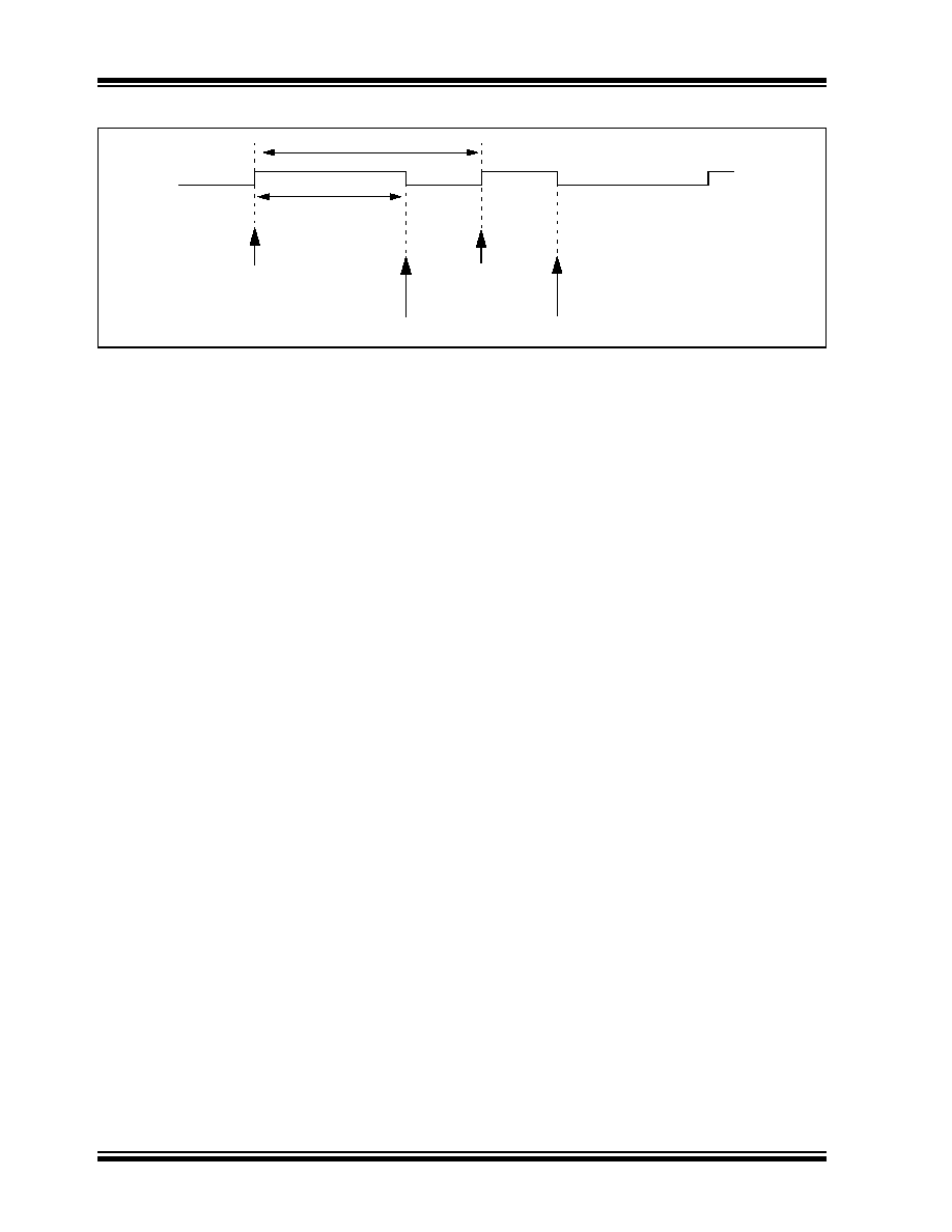
dsPIC30F1010/202X
DS70178A-page 104
Advance Information
©
2006 Microchip Technology Inc.
FIGURE 11-1:
PWM OUTPUT TIMING
11.7
Output Compare Interrupts
The output compare channels have the ability to gener-
ate an interrupt on a compare match, for whichever
Match mode has been selected.
For all modes except the PWM mode, when a compare
event occurs, the respective interrupt flag (OCxIF) is
asserted and an interrupt will be generated, if enabled.
The OCxIF bit is located in the corresponding IFS
STATUS register, and must be cleared in software. The
interrupt is enabled via the respective compare inter-
rupt enable (OCxIE) bit, located in the corresponding
IEC Control register.
For the PWM mode, when an event occurs, the respec-
tive timer interrupt flag (T2IF or T3IF) is asserted and
an interrupt will be generated, if enabled. The IF bit is
located in the IFS0 STATUS register, and must be
cleared in software. The interrupt is enabled via the
respective timer interrupt enable bit (T2IE or T3IE),
located in the IEC0 Control register. The output com-
pare interrupt flag is never set during the PWM mode of
operation.
Period
Duty Cycle
TMR3 = Duty Cycle (OCxR)
TMR3 = Duty Cycle (OCxR)
TMR3 = PR3
T3IF =
1
(Interrupt Flag)
OCxR = OCxRS
TMR3 = PR3
(Interrupt Flag)
OCxR = OCxRS
T3IF =
1

©
2006 Microchip Technology Inc.
Advance Information
DS70178A-page 105
dsPIC30F1010/202X
T
A
BLE
1
1
-1:
O
UTP
U
T COM
P
ARE
RE
G
I
S
T
E
R
MAP
S
F
R Na
m
e
Ad
d
r
.
B
it
15
Bit
14
Bit
13
Bit
12
Bi
t 1
1
Bit
10
Bit
9
B
it
8
B
it
7
B
it 6
B
i
t
5
B
it
4
B
it
3
B
i
t
2
B
it
1
B
it
0
R
e
s
e
t
S
t
at
e
OC
1
R
S
0
1
8
0
O
utp
u
t C
o
mpar
e 1
Ma
ster
R
e
g
i
ster
0000
0000 0000 0000
OC
1
R
01
82
O
u
tp
ut C
o
mpar
e 1
S
l
ave
R
e
g
i
s
t
er
0000
0000 0000 0000
OC1
C
ON
01
84
--
--O
C
S
I
D
L
--
--
--
--
--
--
--
--
O
CF
L
T
1
O
CT
SEL
1
O
CM
<2
:0
>
0000
0000 0000 0000
OC
2
R
S
0
1
8
6
O
utp
u
t C
o
mpar
e 2
Ma
ster
R
e
g
i
ster
0000
0000 0000 0000
OC
2
R
01
88
O
u
tp
ut C
o
mpar
e 2
S
l
ave
R
e
g
i
s
t
er
0000
0000 0000 0000
OC2
C
ON
018
A
--
--O
C
S
I
D
L
--
--
--
--
--
--
--
--
O
CF
L
T
2
O
CT
SEL
2
O
CM
<2
:0
>
0000
0000 0000 0000
Note
:
Ref
e
r to
th
e "
ds
PIC
3
0F F
a
mi
ly
R
e
fe
ren
c
e
Ma
nua
l"
(D
S7
004
6) f
o
r de
sc
rip
t
io
ns
of re
gi
ste
r
bi
t fi
eld
s
.

dsPIC30F1010/202X
DS70178A-page 106
Advance Information
©
2006 Microchip Technology Inc.
NOTES:

©
2006 Microchip Technology Inc.
Advance Information
DS70178A-page 107
dsPIC30F1010/202X
12.0
POWER SUPPLY PWM
The PWM module on the dsPIC30F1010/202X device
supports a wide variety of PWM modes and output for-
mats. This PWM module is ideal for power conversion
applications such as:
∑ DC/DC converters
∑ AC/DC power supplies
∑ Uninterruptable Power Supply (UPS)
12.1
Features Overview
The PS PWM module incorporates these features:
∑ Four PWM generators with eight I/O
∑ Four Independent time bases
∑ Duty cycle resolution of 1.1 nsec @ 30 MIPS
∑ Dead-time resolution of 4.2 nsec @ 30 MIPS
∑ Phase-shift resolution of 4.2 nsec @ 30 MIPS
∑ Frequency resolution of 8.4 nsec @ 30 MIPS
∑ Supported PWM modes:
- Standard Edge-Aligned PWM
- Complementary PWM
- Push-Pull PWM
- Multi-Phase PWM
- Variable Phase PWM
- Fixed Off-Time PWM
- Current Reset PWM
- Current-Limit PWM
- Independent Time Base PWM
∑ On-the-Fly changes to:
- PWM frequency
- PWM duty cycle
- PWM phase shift
∑ Output override control
∑ Independent current-limit and Fault inputs
∑ Special event comparator for scheduling other
peripheral events
∑ Each PWM generator has comparator for
triggering ADC conversions.
Figure 12-1 conceptualizes the PWM module in a sim-
plified block diagram. Figure 12-2 illustrates how the
module hardware is partitioned for each PWM output
pair for the Complementary PWM mode. Each func-
tional unit of the PWM module is discussed in
subsequent sections.
The PWM module contains four PWM generators. The
module has eight PWM output pins: PWM1H, PWM1L,
PWM2H, PWM2L, PWM3H, PWM3L, PWM4H and
PWM4L. For complementary outputs, these eight I/O
pins are grouped into H/L pairs.
12.2
Description
The PS PWM module is designed for applications that
require (a) high resolution at high PWM frequencies,
(b) the ability to drive standard push-pull or half bridge
converters or (c) the ability to create multi-phase PWM
outputs.
Two common, medium-power converter topologies are
Push-Pull and Half-Bridge. These designs require the
PWM output signal to be switched between alternate
pins, as provided by the Push-Pull PWM mode.
Phase-shifted PWM describes the situation where
each PWM generator provides outputs, but the phase
relationship between the generator outputs is
specifiable and changeable.
Multi-Phase PWM is often used to improve DC-DC
converter load transient response, and reduce the size
of output filter capacitors and inductors. Multiple DC/
DC converters are often operated in parallel but phase
shifted in time. A single PWM output operating at 250
KHz has a period of 4 µsec. But an array of four PWM
channels, staggered by 1 µsec each, yields an effective
switching frequency of 1 MHz. Multi-phase PWM appli-
cations typically use a fixed-phase relationship.
Variable Phase PWM is useful in Zero Voltage Transi-
tion (ZVT) power converters. Here the PWM duty cycle
is always 50%, and the power flow is controlled by
varying the relative phase shift between the two PWM
generators.
Note: The PLL must be enabled for the PS PWM
module to function. This is achieved by using the
FNOSC<1:0> bits in the FOSCSEL Configuration
register.

dsPIC30F1010/202X
DS70178A-page 108
Advance Information
©
2006 Microchip Technology Inc.
FIGURE 12-1:
SIMPLIFIED CONCEPTUAL BLOCK DIAGRAM OF POWER SUPPLY PWM
MUX
Latch
Comparator
Timer
PDC2
Phase
MUX
Latch
Comparator
Timer
PDC3
Phase
MUX
Latch
Comparator
Timer
PDC4
Phase
MUX
Latch
Comparator
Timer
PDC1
PWMCONx
LEBCONx
Channel 1
Dead-time Generator
PTCON
SEVTCMP
Comparator
Special event
IOCONx
PWM enable and mode control
Channel 3
Dead-time Generator
Channel 4
Dead-time Generator
ALTDTRx, DTRx
Dead-time Control
Special Event
Postscaler
SFLT
X
PWM3L
PWM3H
PWM2L
PWM2H
1
6
-
b
it Da
t
a
Bu
s
PWM1L
PWM1H
FLTCONx
Pin and mode control
MDC
ADC Trigger Control
Master Duty Cycle Reg
Fault mode and pin control
Pin override control
Special event
PTPER
Timer Period
PWM GEN #1
PWM GEN #2
PWM GEN #4
PTMR
Master Time Base
Phase
PWM GEN #3
Channel 2
Dead-time Generator
PWM4L
PWM4H
P
W
M
U
s
e
r
, C
u
rre
nt
Li
mi
t
and
F
aul
t
Over
ri
d
e
a
nd R
outi
n
g L
o
g
i
c
F
a
u
l
t
C
L
M
T
Over
ri
de
Lo
gi
c
trigger
comparison value
IFLT
X
Fault Control
Logic
TRGCONx
Control for blanking external input signals
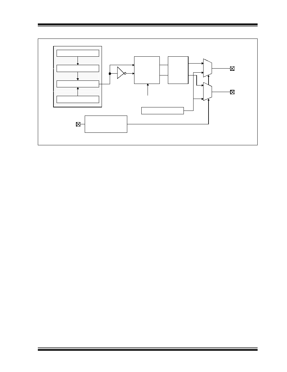
©
2006 Microchip Technology Inc.
Advance Information
DS70178A-page 109
dsPIC30F1010/202X
FIGURE 12-2:
PARTITIONED OUTPUT PAIR, COMPLEMENTARY PWM MODE
12.3
Control Registers
The following registers control the operation of the
Power Supply PWM Module.
∑ PTCON: PWM Time Base Control Register
∑ PTPER: Primary Time Base Register
∑ SEVTCMP: PWM Special Event Register
∑ MDC: PWM Master Duty Cycle Register(1)
∑ PWMCONx: PWM Control Register
∑ PDCx: PWM Generator Duty Cycle Register(1)
∑ PHASEx: PWM Phase-Shift Register
∑ DTRx: PWM Dead-Time Register
∑ ALTDTRx: PWM Alternate Dead-Time Register
∑ TRGCONx: PWM TRIGGER Control Register
∑ IOCONx: PWM I/O Control Register
∑ FCLCONx: PWM Fault Current-Limit Control
Register
∑ TRIGx: PWM Trigger Compare Value Register
∑ LEBCONx: Leading Edge Blanking Control Regis-
ter
PWM Duty Cycle Register
Duty Cycle Comparator
Fault Override Values
Channel override values
Fault Pin Assignment Logic
Fault Pin
PWM
X
H
PWM
X
L
TMR < PDC
PWM
Override
Logic
Dead
Time
Logic
Fault Active
Phase Offset
M
U
X
M
U
X
Timer/Counter

dsPIC30F1010/202X
DS70178A-page 110
Advance Information
©
2006 Microchip Technology Inc.
REGISTER 12-1:
PTCON: PWM TIME BASE CONTROL REGISTER
R/W-0
U-0
R/W-0
R/W-0
R/W-0
R/W-0
R/W-0
R/W-0
PTEN
--
PTSIDL
SESTAT
SEIEN
EIPU
SYNCPOL
SYNCOEN
bit 15
bit 8
R/W-0
R/W-0
R/W-0
R/W-0
R/W-0
R/W-0
R/W-0
R/W-0
SYNCEN
SYNCSRC<2:0>
SEVTPS<3:0>
bit 7
bit 0
Legend:
R = Readable bit
W = Writable bit
U = Unimplemented bit, read as `0'
-n = Value at POR
`1' = Bit is set
`0' = Bit is cleared
x = Bit is unknown
bit 15
PTEN: PWM Module Enable bit
1
= PWM module is enabled
0
= PWM module is disabled
bit 14
Unimplemented: Read as `
0
'
bit 13
PTSIDL: PWM Time Base Stop in Idle Mode bit
1
= PWM time base halts in CPU Idle mode
0
= PWM time base runs in CPU Idle mode
bit 12
SESTAT: Special Event Interrupt Status bit
1
= Special Event Interrupt is pending
0
= Special Event Interrupt is not pending
bit 11
SEIEN: Special Event Interrupt Enable bit
1
= Special Event Interrupt is enabled
0
= Special Event Interrupt is disabled
bit 10
EIPU: Enable Immediate Period Updates bit
1
= Active Period register is updated immediately
0
= Active Period register updates occur on PWM cycle boundaries
bit 9
SYNCPOL: Synchronize Input Polarity bit
1
= SYNCIN polarity is inverted (low active)
0
= SYNCIN is high active
bit 8
SYNCOEN: Primary Time Base Sync Enable bit
1
= SYNCO output is enabled
0
= SYNCO output is disabled
bit 7
SYNCEN: External Time Base Synchronization Enable bit
1
= External synchronization of primary time base is enabled
0
= External synchronization of primary time base is disabled
bit 6-4
SYNCSRC<2:0>: Sync Source Selection bits
000
= SYNCI
001
= Reserved
.
.
111
= Reserved
bit 3-0
SEVTPS<3:0>: PWM Special Event Trigger Output Postscale Select bits
0000
= 1:1 Postscale
0001
= 1:2 Postscale
| |
| |
1111
= 1:16 Postscale

©
2006 Microchip Technology Inc.
Advance Information
DS70178A-page 111
dsPIC30F1010/202X
REGISTER 12-2:
PTPER: PRIMARY TIME BASE REGISTER
R/W-0
R/W-0
R/W-0
R/W-0
R/W-0
R/W-0
R/W-0
R/W-0
PTPER <15:8>
bit 15
bit 8
R/W-0
R/W-0
R/W-0
R/W-0
R/W-0
U-0
U-0
U-0
PTPER <7:3>
--
--
--
bit 7
bit 0
Legend:
R = Readable bit
W = Writable bit
U = Unimplemented bit, read as `0'
-n = Value at POR
`1' = Bit is set
`0' = Bit is cleared
x = Bit is unknown
bit 15-3
Primary Time Base (PTMR) Period Value bits
bit 2-0
Unimplemented: Read as `
0
'

dsPIC30F1010/202X
DS70178A-page 112
Advance Information
©
2006 Microchip Technology Inc.
REGISTER 12-3:
SEVTCMP: PWM SPECIAL EVENT REGISTER
R/W-0
R/W-0
R/W-0
R/W-0
R/W-0
R/W-0
R/W-0
R/W-0
SEVTCMP <15:8>
bit 15
bit 8
R/W-0
R/W-0
R/W-0
R/W-0
R/W-0
U-0
U-0
U-0
SEVTCMP <7:3>
--
--
--
bit 7
bit 0
Legend:
R = Readable bit
W = Writable bit
U = Unimplemented bit, read as `0'
-n = Value at POR
`1' = Bit is set
`0' = Bit is cleared
x = Bit is unknown
bit 15-3
Special Event Compare Count Value bits
bit 2-0
Unimplemented: Read as `
0
'

©
2006 Microchip Technology Inc.
Advance Information
DS70178A-page 113
dsPIC30F1010/202X
REGISTER 12-4:
MDC: PWM MASTER DUTY CYCLE REGISTER
(1)
R/W-0
R/W-0
R/W-0
R/W-0
R/W-0
R/W-0
R/W-0
R/W-0
MDC<15:8>
bit 15
bit 8
R/W-0
R/W-0
R/W-0
R/W-0
R/W-0
R/W-0
R/W-0
R/W-0
MDC<7:0>
bit 7
bit 0
Legend:
R = Readable bit
W = Writable bit
U = Unimplemented bit, read as `0'
-n = Value at POR
`1' = Bit is set
`0' = Bit is cleared
x = Bit is unknown
bit 15-0
Master PWM Duty Cycle Value bits
Note 1: The minimum value for this register is 0x0008 and the maximum value is 0xFFEF.

dsPIC30F1010/202X
DS70178A-page 114
Advance Information
©
2006 Microchip Technology Inc.
REGISTER 12-5:
PWMCONx: PWM CONTROL REGISTER
HS/HC-0
HS/HC-0
HS/HC-0
R/W-0
R/W-0
R/W-0
R/W-0
R/W-0
FLTSTAT
CLSTAT
TRGSTAT
FLTIEN
CLIEN
TRGIEN
ITB
MDCS
bit 15
bit 8
R/W-0
R/W-0
U-0
U-0
U-0
U-0
R/W-0
R/W-0
DTC<1:0>
--
--
--
--
XPRES
IUE
bit 7
bit 0
Legend:
R = Readable bit
W = Writable bit
U = Unimplemented bit, read as `0'
-n = Value at POR
`1' = Bit is set
`0' = Bit is cleared
x = Bit is unknown
bit 15
FLTSTAT: Fault Interrupt Status
1
= Fault Interrupt is pending
0
= No Fault Interrupt is pending
This bit is cleared by setting FLTIEN =
0
.
Note:
Software must clear the interrupt status here, and the corresponding IFS bit in Interrupt
Controller.
bit 14
CLSTAT: Current-Limit Interrupt Status bit
1
= Current-limit interrupt is pending
0
= No current-limit interrupt is pending
This bit is cleared by setting CLIEN =
0
.
Note:
Software must clear the interrupt status here, and the corresponding IFS bit in Interrupt
Controller.
bit 13
TRIGIEN: Trigger Interrupt Status bit
1
= Trigger interrupt is pending
0
= No trigger interrupt is pending
This bit is cleared by setting TRGIEN =
0
.
bit 12
FLTIEN: Fault Interrupt Enable bit
1
= Fault interrupt enabled
0
= Fault interrupt disabled and FLTSTAT bit is cleared
bit 11
CLIEN: Current-Limit Interrupt Enable bit
1
= Current-limit interrupt enabled
0
= Current-limit interrupt disabled and CLSTAT bit is cleared
bit 10
TRIGIEN: Trigger Interrupt Enable bit
1
= A trigger event generates an interrupt request
0
= Trigger event interrupts are disabled and TRGSTAT bit is cleared
bit 9
ITB: Independent Time Base Mode bit
0
= Primary time base provides timing for this PWM generator
1
= Phasex register provides time base period for this PWM generator
bit 8
MDCS: Master Duty Cycle Register Select bit
0
= DCx register provides duty cycle information for this PWM generator
1
= MDC register provides duty cycle information for this PWM generator
bit 7-6
DTC<1:0>: Dead-time Control bits
00
= Positive dead time actively applied for all output modes
01
= Negative dead time actively applied for all output modes
10
= Dead-time function is disabled
11
= Reserved
bit 5-2
Unimplemented: Read as `
0
'

©
2006 Microchip Technology Inc.
Advance Information
DS70178A-page 115
dsPIC30F1010/202X
bit 1
XPRES: External PWM Reset Control bit
1
= Current-limit source resets time base for this PWM generator if it is in independent time base
mode
0
= External pins do not affect PWM time base
bit 0
IUE: Immediate Update Enable bit
1
= Updates to the active PDC registers are immediate
0
= Updates to the active PDC registers are synchronized to the PWM time base
REGISTER 12-6:
PDCx: PWM GENERATOR DUTY CYCLE REGISTER
(1)
R/W-0
R/W-0
R/W-0
R/W-0
R/W-0
R/W-0
R/W-0
R/W-0
PDCx<15:8>
bit 15
bit 8
R/W-0
R/W-0
R/W-0
R/W-0
R/W-0
R/W-0
R/W-0
R/W-0
PDCx<7:0>
bit 7
bit 0
Legend:
R = Readable bit
W = Writable bit
U = Unimplemented bit, read as `0'
-n = Value at POR
`1' = Bit is set
`0' = Bit is cleared
x = Bit is unknown
bit 15-0
PWM Generator #x Duty Cycle Value bits
Note 1: The minimum value for this register is 0x0008 and the maximum value is 0xFFEF.
REGISTER 12-5:
PWMCONx: PWM CONTROL REGISTER (CONTINUED)
dsPIC30F1010/202X
DS70178A-page 116
Advance Information
©
2006 Microchip Technology Inc.
REGISTER 12-7:
PHASEx: PWM PHASE-SHIFT REGISTER
R/W-0
R/W-0
R/W-0
R/W-0
R/W-0
R/W-0
R/W-0
R/W-0
PHASEx<15:8>
bit 15
bit 8
R/W-0
R/W-0
R/W-0
R/W-0
R/W-0
R/W-0
U-0
U-0
PHASEx<7:2>
--
--
bit 7
bit 0
Legend:
R = Readable bit
W = Writable bit
U = Unimplemented bit, read as `0'
-n = Value at POR
`1' = Bit is set
`0' = Bit is cleared
x = Bit is unknown
bit 15-2
PHASEx<15:2>: PWM Phase-Shift Value or Independent Time Base Period for this PWM Generator bits
Note:
If used as an independent time base, bits <3:2> are not used.
bit 1-0
Unimplemented: Read as `
0
'
REGISTER 12-8:
DTRx: PWM DEAD-TIME REGISTER
U-0
U-0
R/W-0
R/W-0
R/W-0
R/W-0
R/W-0
R/W-0
--
--
DTRx<13:8>
bit 15
bit 8
R/W-0
R/W-0
R/W-0
R/W-0
R/W-0
R/W-0
U-0
U-0
DTRx<7:2>
--
--
bit 7
bit 0
Legend:
R = Readable bit
W = Writable bit
U = Unimplemented bit, read as `0'
-n = Value at POR
`1' = Bit is set
`0' = Bit is cleared
x = Bit is unknown
bit 15-14
Unimplemented: Read as `
0
'
bit 13-2
DTRx<13:2>: Unsigned 11-bit Dead-Time Value bits for PWMx Dead-Time Unit
bit 1-0
Unimplemented: Read as `
0
'

©
2006 Microchip Technology Inc.
Advance Information
DS70178A-page 117
dsPIC30F1010/202X
REGISTER 12-9:
ALTDTRx: PWM ALTERNATE DEAD-TIME REGISTER
R/W-0
R/W-0
R/W-0
R/W-0
R/W-0
R/W-0
R/W-0
R/W-0
--
--
ALTDTRx<13:8>
bit 15
bit 8
R/W-0
R/W-0
R/W-0
R/W-0
R/W-0
R/W-0
U-0
U-0
ALTDTR <7:2>
--
--
bit 7
bit 0
Legend:
R = Readable bit
W = Writable bit
U = Unimplemented bit, read as `0'
-n = Value at POR
`1' = Bit is set
`0' = Bit is cleared
x = Bit is unknown
bit 15-14
Unimplemented: Read as `
0
'
bit 13-2
ALTDTRx<13:2>: Unsigned 11-bit Dead-Time Value bits for PWMx Dead-Time Unit
bit 1-0
Unimplemented: Read as `
0
'

dsPIC30F1010/202X
DS70178A-page 118
Advance Information
©
2006 Microchip Technology Inc.
REGISTER 12-10: TRGCONx: PWM TRIGGER CONTROL REGISTER
R/W-0
R/W-0
R/W-0
U-0
U-0
U-0
U-0
U-0
TRGDIV<2:0>
--
--
--
--
--
bit 15
bit 8
U-0
U-0
R/W-0
R/W-0
R/W-0
R/W-0
R/W-0
R/W-0
--
--
TRGSTRT<5:0>
bit 7
bit 0
Legend:
R = Readable bit
W = Writable bit
U = Unimplemented bit, read as `0'
-n = Value at POR
`1' = Bit is set
`0' = Bit is cleared
x = Bit is unknown
bit 15-13
TRGDIV<2:0>: Trigger Output Divider
000
= Trigger output for every trigger event
001
= Trigger output for every 2nd trigger event
010
= Trigger output for every 3rd trigger event
011
= Trigger output for every 4th trigger event
100
= Trigger output for every 5th trigger event
101
= Trigger output for every 6th trigger event
110
= Trigger output for every 7th trigger event
111
= Trigger output for every 8th trigger event
bit 12-6
Unimplemented: Read as `
0
'
bit 5-0
TRGSTRT<5:0>: Trigger Postscaler Start Enable Select bits
This value specifies the ROLL counter value needed for a match that will then enable the trigger
postscaler logic to begin counting trigger events.

©
2006 Microchip Technology Inc.
Advance Information
DS70178A-page 119
dsPIC30F1010/202X
REGISTER 12-11: IOCONx: PWM I/O CONTROL REGISTER
R/W-0
R/W-0
R/W-0
R/W-0
R/W-0
R/W-0
R/W-0
R/W-0
PENH
PENL
POLH
POLL
PMOD<1:0>
OVRENH
OVRENL
bit 15
bit 8
R/W-0
R/W-0
R/W-0
R/W-0
R/W-0
R/W-0
U-0
R/W-0
OVRDAT<1:0>
FLTDAT<1:0>
CLDAT<1:0>
--
OSYNC
bit 7
bit 0
Legend:
R = Readable bit
W = Writable bit
U = Unimplemented bit, read as `0'
-n = Value at POR
`1' = Bit is set
`0' = Bit is cleared
x = Bit is unknown
bit 15
PENH: PWMH Output Pin Ownership bit
1
= PWM module controls PWMxH pin
0
= GPIO module controls PWMxH pin
bit 14
PENL: PWML Output Pin Ownership bit
1
= PWM module controls PWMxL pin
0
= GPIO module controls PWMxL pin
bit 13
POLH: PWMH Output Pin Polarity bit
0
= PWMxH pin is high active
1
= PWMxH pin is low active
bit 12
POLL: PWML Output Pin Polarity bit
0
= PWMxL pin is high active
1
= PWMxL pin is low active
bit 11-10
PMOD<1:0>: PWM #x I/O Pin Mode bits
00
= PWM I/O pin pair is in the Complementary Output mode
01
= PWM I/O pin pair is in the Independent Output mode
10
= PWM I/O pin pair is in the Push-Pull Output mode
11
= Reserved
bit 9
OVRENH: Override Enable for PWMxH Pin bit
0
= PWM generator provides data for PWMxH pin
1
= OVRDAT[1] provides data for output on PWMxH pin
bit 8
OVRENL: Override Enable for PWMxL Pin bit
0
= PWM generator provides data for PWMxL pin
1
= OVRDAT[0] provides data for output on PWMxL pin
bit 7-6
OVRDAT<1:0>: Data for PWMxH,L Pins if Override is Enabled bits
If OVERENH =
1
then OVRDAT<1> provides data for PWMxH
If OVERENL =
1
then OVRDAT<0> provides data for PWMxL
bit 5-4
FLTDAT<1:0>: Data for PWMxH,L Pins if FLTMODE is Enabled bits
If Fault active, then FLTDAT<1> provides data for PWMxH
If Fault active, then FLTDAT<0> provides data for PWMxL
bit 3-2
CLDAT<1:0>: Data for PWMxH,L Pins if CLMODE is Enabled bits
If current limit active, then CLDAT<1> provides data for PWMxH
If current limit active, then CLDAT<0> provides data for PWMxL
bit 1
Unimplemented: Read as `
0
'
bit 0
OSYNC: Output Override Synchronization bit
1
= Output overrides via the OVRDAT<1:0> bits are synchronized to the PWM time base
0
= Output overrides via the OVDDAT<1:0> bits occur on next clock boundary

dsPIC30F1010/202X
DS70178A-page 120
Advance Information
©
2006 Microchip Technology Inc.
REGISTER 12-12: FCLCONx: PWM FAULT CURRENT-LIMIT CONTROL REGISTER
U-0
U-0
U-0
R/W-0
R/W-0
R/W-0
R/W-0
R/W-0
--
--
--
CLSRC<3:0>
CLPOL
bit 15
bit 8
R/W-0
R/W-0
R/W-0
R/W-0
R/W-0
R/W-0
R/W-0
R/W-0
CLMODE
FLTSRC<3:0>
FLTPOL
FLTMOD<1:0>
bit 7
bit 0
Legend:
R = Readable bit
W = Writable bit
U = Unimplemented bit, read as `0'
-n = Value at POR
`1' = Bit is set
`0' = Bit is cleared
x = Bit is unknown
bit 15-13
Unimplemented: Read as `
0
'
bit 12-9
CLSRC<3:0>: Current-Limit Control Signal Source Select for PWM #X Generator bits
0000
= Analog Comparator #1
0001
= Analog Comparator #2
0010
= Analog Comparator #3
0011
= Analog Comparator #4
0100
= Reserved
0101
= Reserved
0110
= Reserved
0111
= Reserved
1000
= Shared Fault #1 (SFLT1)
1001
= Shared Fault #2 (SFLT2)
1020
= Shared Fault #3 (SFLT3)
1011
= Shared Fault #4 (SFLT4)
1100
= Reserved
1101
= Independent Fault #2 (IFLT2)
1110
= Reserved
1111
= Independent Fault #4 (IFLT4)
bit 8
CLPOL: Current-Limit Polarity for PWM Generator #X bit
0
= The selected current-limit source is high active
1
= The selected current-limit source is low active
bit 7
CLMODE: Current-Limit Mode Enable for PWM Generator #X bit
1
= Current-limit function is enabled
0
= Current-limit function is disabled

©
2006 Microchip Technology Inc.
Advance Information
DS70178A-page 121
dsPIC30F1010/202X
bit 6-3
FLTSRC<3:0>: Fault Control Signal Source Select for PWM Generator #X bits
0000
= Analog Comparator #1
0001
= Analog Comparator #2
0010
= Analog Comparator #3
0011
= Analog Comparator #4
0100
= Reserved
0101
= Reserved
0110
= Reserved
0111
= Reserved
1000
= Shared Fault #1 (SFLT1)
1001
= Shared Fault #2 (SFLT2)
1020
= Shared Fault #3 (SFLT3)
1011
= Shared Fault #4 (SFLT4)
1100
= Reserved
1101
= Independent Fault #2 (IFLT2)
1110
= Reserved
1111
= Independent Fault #4 (IFLT4)
bit 2
FLTPOL: Fault Polarity for PWM Generator #X bit
0
= The selected Fault source is high active
1
= The selected Fault source is low active
bit 1-0
FLTMOD<1:0>: Fault Mode for PWM Generator #x bits
00
= Reserved
01
= The selected Fault source forces PWMxH, PWMxL pins to FLTDAT values (cycle)
10
= Reserved
11
= Fault input is disabled
REGISTER 12-12: FCLCONx: PWM FAULT CURRENT-LIMIT CONTROL REGISTER (CONTINUED)

dsPIC30F1010/202X
DS70178A-page 122
Advance Information
©
2006 Microchip Technology Inc.
REGISTER 12-13: TRIGx: PWM TRIGGER COMPARE VALUE REGISTER
R/W-0
R/W-0
R/W-0
R/W-0
R/W-0
R/W-0
R/W-0
R/W-0
TRGCMP<15:8>
bit 15
bit 8
R/W-0
R/W-0
R/W-0
R/W-0
R/W-0
U-0
U-0
U-0
TRGCMP<7:3>
--
--
--
bit 7
bit 0
Legend:
R = Readable bit
W = Writable bit
U = Unimplemented bit, read as `0'
-n = Value at POR
`1' = Bit is set
`0' = Bit is cleared
x = Bit is unknown
bit 15-3
TRGCMP<15:3>: Trigger Control Value bits
Register contains the compare value for PWMx time base for generating a trigger to the
ADC module for initiating a sample and conversion process, or generating a trigger interrupt.
bit 2-0
Unimplemented: Read as `
0
'

©
2006 Microchip Technology Inc.
Advance Information
DS70178A-page 123
dsPIC30F1010/202X
REGISTER 12-14: LEBCONx: LEADING EDGE BLANKING CONTROL REGISTER
R/W-0
R/W-0
R/W-0
R/W-0
R/W-0
R/W-0
R/W-0
R/W-0
PHR
PHF
PLR
PLF
FLTLEBEN
CLLEBEN
LEB<9:8>
bit 15
bit 8
R/W-0
R/W-0
R/W-0
R/W-0
R/W-0
U-0
U-0
U-0
LEB<7:3>
--
--
--
bit 7
bit 0
Legend:
R = Readable bit
W = Writable bit
U = Unimplemented bit, read as `0'
-n = Value at POR
`1' = Bit is set
`0' = Bit is cleared
x = Bit is unknown
bit 15
PHR: PWMH Rising Edge Trigger Enable bit
1
= Rising edge of PWMH will trigger LEB counter
0
= LEB ignores rising edge of PWMH
bit 14
PHL: PWMH Falling Edge Trigger Enable bit
1
= Falling edge of PWMH will trigger LEB counter
0
= LEB ignores falling edge of PWMH
bit 13
PLR: PWML Rising Edge Trigger Enable bit
1
= Rising edge of PWML will trigger LEB counter
0
= LEB ignores rising edge of PWML
bit 12
PLF: PWML Falling Edge Trigger Enable bit
1
= Falling edge of PWML will trigger LEB counter
0
= LEB ignores falling edge of PWML
bit 11
FLTLEBEN: Fault Input Leading Edge Blanking Enable bit
1
= Leading Edge Blanking is applied to selected Fault Input
0
= Leading Edge Blanking is not applied to selected Fault Input
bit 10
CLLEBEN: Current-Limit Leading Edge Blanking Enable bit
1
= Leading Edge Blanking is applied to selected Current-Limit Input
0
= Leading Edge Blanking is not applied to selected Current-Limit Input
bit 9-3
LEB: Leading Edge Blanking for Current-Limit and Fault Inputs bits
Value is 8 nsec increments
bit 2-0
Unimplemented: Read as `
0
'

dsPIC30F1010/202X
DS70178A-page 124
Advance Information
©
2006 Microchip Technology Inc.
12.4
Module Functionality
The PS PWM module is a very high-speed design that
provides capabilities not found in other PWM genera-
tors. The module supports these PWM modes:
∑ Standard Edge-Aligned PWM mode
∑ Complementary PWM mode
∑ Push-Pull PWM mode
∑ Multi-Phase PWM mode
∑ Variable Phase PWM mode
∑ Current-Limit PWM mode
∑ Constant Off-time PWM mode
∑ Current Reset PWM mode
∑ Independent Time Base PWM mode
12.4.1
STANDARD EDGE-ALIGNED PWM
MODE
Standard Edge-Aligned mode (Figure 12-3) is the basic
PWM mode used by many power converter topologies
such as "Buck", "Boost" and "Forward". To create the
edge-aligned PWM, a timer/counter circuit counts
upward from zero to a specified maximum value for the
Period. Another register contains the value for Duty
Cycle, which is constantly compared to the timer
(Period) value. While the timer/counter value is less
than or equal to the duty cycle value, the PWM output
signal is asserted. When the timer value exceeds the
duty cycle value, the PWM signal is deasserted. When
the timer is greater than the period value, the timer is
reset, and the process repeats.
FIGURE 12-3:
EDGE-ALIGNED PWM
12.4.2
COMPLEMENTARY PWM MODE
Complementary PWM is generated in a manner similar
to standard Edge-Aligned PWM. Complementary mode
provides a second PWM output signal on the PWML
pin that is the complement of the primary PWM signal
(PWMH). Complementary mode PWM is shown in
Figure 12-4.
FIGURE 12-4:
COMPLEMENTARY PWM
12.4.3
PUSH-PULL PWM MODE
The Push-Pull mode shown in Figure 12-5 is a version
of the standard Edge-Aligned PWM mode where the
active PWM signal is alternately outputted on one of
two PWM pins. There is no complementary PWM out-
put available. This mode is useful in transformer-based
power converters. Transformer-based circuits must
avoid any direct currents that will cause their cores to
saturate. The Push-Pull mode ensures that the duty
cycle of the two phases is identical, thus yielding a net
DC bias of zero.
FIGURE 12-5:
PUSH-PULL PWM
Period
Duty Cycle
0
Period
Timer
Value
Timer Resets
PWMH
Value
Duty Cycle Match
Period
Duty Cycle
0
Period
Timer
Value
Timer Resets
PWMH
Value
PWML
(Period)-(Duty Cycle)
Duty Cycle Match
Period
Duty Cycle
0
Period
Timer
Value
Timer Resets
PWMH
Value
PWML
Duty Cycle
Duty Cycle Match

©
2006 Microchip Technology Inc.
Advance Information
DS70178A-page 125
dsPIC30F1010/202X
12.4.4
MULTI-PHASE PWM MODE
Multi-Phase PWM, as shown in Figure 12-6, uses
phase-shift values in the Phase registers to shift the
PWM outputs relative to the primary time base.
Because the phase-shift values are added to the pri-
mary time base, the phase-shifted outputs occur earlier
than a PWM channel that specifies zero phase shift. In
Multi-Phase mode, the specified phase shift is fixed by
the application's design.
FIGURE 12-6:
MULTI-PHASE PWM
12.4.5
VARIABLE PHASE PWM MODE
Figure 12-7 shows the waveforms for Variable Phase-
Shift PWM. Power-converter circuits constantly change
the phase shift among PWM channels as a means to
control the flow of power, in contrast to most PWM cir-
cuits that vary the duty cycle of PWM signals to control
power flow. Often, in variable phase applications, the
PWM duty cycle is maintained at 50%. The phase-shift
value should be updated when the PWM signal is not
asserted. Complementary outputs are available in Vari-
able Phase-Shift mode.
FIGURE 12-7:
VARIABLE PHASE PWM
12.4.6
CURRENT-LIMIT PWM MODE
Figure 12-8 shows Cycle-by-Cycle Current-Limit
mode. This mode truncates the asserted PWM signal
when the selected external Fault signal is asserted.
The PWM output values are specified by the Fault
override bits (FLTDAT<1:0>) in the IOCONx register.
The override output remains in effect until the begin-
ning of the next PWM cycle. This mode is sometimes
used in Power Factor Correction (PFC) circuits where
the inductor current controls the PWM on time. This is
a constant frequency PWM mode.
FIGURE 12-8:
CYCLE-BY-CYCLE
CURRENT-LIMIT PWM
MODE
12.4.7
CONSTANT OFF-TIME PWM
Constant Off-Time mode is shown in Figure 12-9.
Constant Off-Time PWM is a variable-frequency mode
where the actual PWM period is less than or equal to
the specified period value. The PWM time base is
externally reset some time after the PWM signal duty
cycle value has been reached, and the PWM signal has
been deasserted. This mode is implemented by
enabling the On-Time PWM mode (Current Reset
mode) and using the complementary output.
Duty Cycle
PWM2H
Duty Cycle
PWM4H
Duty Cycle
PWM3H
Duty Cycle
PWM1H
Period
Phase4
Phase2
Phase3
PTMR=0
Duty Cycle
PWM1H
Period
Duty Cycle
Duty Cycle
Phase2 (old value)
Duty Cycle
PWM2H
Phase2 (new value)
Duty Cycle
0
Period
Timer
Value
PWMH
Value
FLTx Negates PWM
Duty Cycle
Programmed
Duty
Cycle
Programmed
Duty Cycle
PWMH
Duty Cycle
Actual
Actual
FLTx Negates PWM
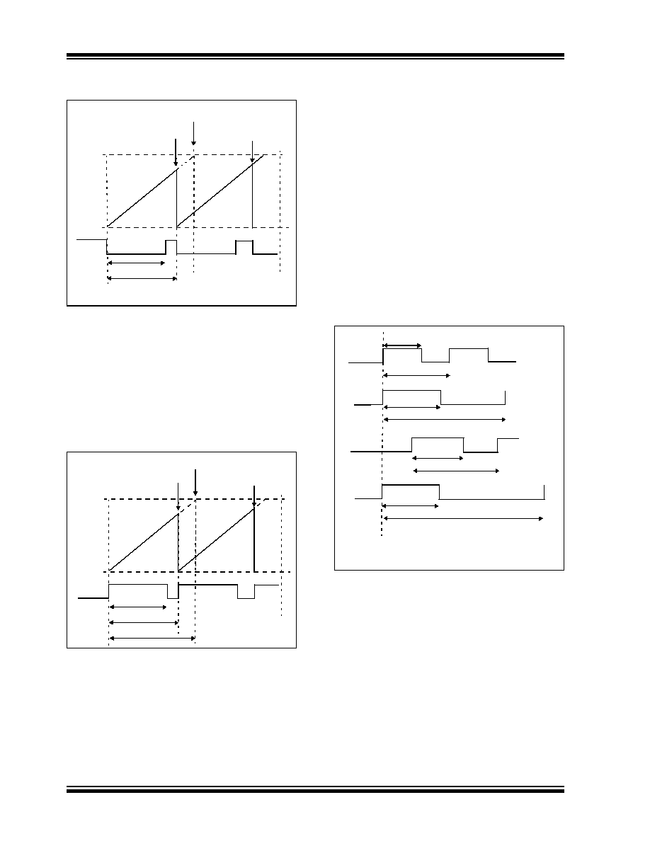
dsPIC30F1010/202X
DS70178A-page 126
Advance Information
©
2006 Microchip Technology Inc.
FIGURE 12-9:
CONSTANT OFF-TIME
PWM
12.4.8
CURRENT RESET PWM MODE
Current Reset PWM is shown in Figure 12-10. Current
Reset PWM uses a Variable-Frequency mode where
the actual PWM period is less than or equal to the spec-
ified period value. The PWM time base is externally
reset some time after the PWM signal duty cycle value
has been reached and the PWM signal has been deas-
serted. Current Reset PWM is a constant on-time PWM
mode.
FIGURE 12-10:
CURRENT RESET PWM
Typically, in the converter application, an energy stor-
age inductor is charged with current while the PWM
signal is asserted, and the inductor current is dis-
charged by the load when the PWM signal is deas-
serted. In this application of current reset PWM, an
external current measurement circuit determines when
the inductor is discharged, and then generates a signal
that the PWM module uses to reset the time base
counter. In Current Reset mode, complementary
outputs are available.
12.4.9
INDEPENDENT TIME BASE PWM
Independent Time Base PWM, as shown in
Figure 12-11, is often used when the dsPIC DSC is
controlling different power converter subcircuits such
as the Power Factor Correction circuit, which may use
100 kHz PWM, and the full-bridge forward converter
section may use 250 kHz PWM.
FIGURE 12-11:
INDEPENDENT TIME
BASE PWM
Duty Cycle
0
Period
Timer
Value
Programmed Period
PWML
Value
External Timer Reset
Duty Cycle
Actual Period
External Timer Reset
Note: Duty Cycle represents off time
Duty Cycle
0
Period
Timer
Value
Programmed Period
PWMH
Value
External Timer Reset
Duty Cycle
Actual Period
External Timer Reset
Programmed Period
Duty Cycle
PWM2H
Duty Cycle
PWM4H
Duty Cycle
PWM3H
Duty Cycle
PWM1H
Period 4
Period 2
Period 3
Period 1
Note:
With independent time bases,
PWM signals are no longer
phase related to each other.
©
2006 Microchip Technology Inc.
Advance Information
DS70178A-page 127
dsPIC30F1010/202X
12.5
Primary PWM Time Base
There is a Primary Time Base (PTMR) counter for the
entire PWM module, In addition, each PWM generator
has an individual time base counter.
The PTMR determines when the individual time base
counters are to update their duty cycle and phase-shift
registers. The master time base is also responsible for
generating the Special Event Triggers and timer-based
interrupts. Figure 12-12 shows a block diagram of the
primary time base logic.
FIGURE 12-12:
PTMR BLOCK DIAGRAM
The primary time base may be reset by an external
signal specified via the SYNCSRC<2:0> bits in the
PTCON register. The external reset feature is enabled
via the SYNCEN bit in the PTCON register. The pri-
mary time base reset feature supports synchronization
of the primary time base with another SMPS dsPIC
DSC device or other circuitry in the user's application.
The primary time base logic also provides an output
signal when a period match occurs that can be used to
synchronize an external device such as another
SMPS dsPIC DSC.
12.5.1
PTMR SYNCHRONIZATION
Because absolute synchronization is not possible, the
user should program the time base period of the sec-
ondary (slave) device to be slightly larger than the pri-
mary device time base to ensure that the two time
bases will reset at the same time.
12.6
Primary PWM Time Base Roll
Counter
The primary time base has an additional 6-bit counter
that counts the period matches of the primary time
base. This ROLL counter enables the PWM genera-
tors to stagger their trigger events in time to the ADC
module. This counter is not accessible for reading.
Each PWM generator has six bits (TRGSTRT<5:0>) in
the TRGCONx registers. These bits are used to spec-
ify the start enable for each TRIGx postscaler con-
trolled by the TRGDIV<2:0> bits in the TRGCONx
registers.
The TDIV bits specify how frequently a trigger pulse is
generated, and the ROLL bits specify when the
sequence begins. Once the TRIG postscaler is
enabled, the ROLL bits and the TRGSTRT bits have
no further effect until the PWM module is disabled and
then reenabled.
The purpose of the ROLL counter and the TRGSTRT
bits is to allow the user to spread the system work load
over a series of PWM cycles.
An additional use of the ROLL counter is to allow the
internal FRC oscillator to be varied on a PWM cycle
basis to reduce peak EMI emissions generated by
switching transistors in the power conversion
application.
The ROLL counter is cleared when the PWM module
is disabled (PTEN =
0
), and the TRIGx postscalers are
disabled, requiring a new ROLL versus TRGSTRT
match to begin counting again.
12.7
Individual PWM Time Base(s)
Each PWM generator also has its own PWM time
base. Figure 12-13 shows a block diagram for the indi-
vidual time base circuits. With a time base per PWM
generator, the PWM module can generate PWM out-
puts that are phase shifted relative to each other, or
totally independent of each other. The individual PWM
timers (TMRx) provide the time base values that are
compared to the duty cycle registers to create the
PWM signals. The user may initialize these individual
time base counters before or during operation via the
phase-shift registers. The primary (PTMR) and the
individual timers (TMRx) are not user readable.
PTMR
PERIOD
Equality Comparator
Clk
>
Reset
12
12
PR_MATCH

dsPIC30F1010/202X
DS70178A-page 128
Advance Information
©
2006 Microchip Technology Inc.
FIGURE 12-13:
TMRX BLOCK DIAGRAM
Normally, the Primary Time Base (PTMR) provides
synchronization control to the individual timer/counters
so they count in lock-step unison.
If the PWM phase-shift feature is used, then the PTMR
provides the synchronization signal to each individual
timer/counter that causes them to reinitialize with their
individual phase-shift values.
If a PWM generator is operating in Independent Time
Base mode, the individual timer/counters count
upward until their count values match the value stored
in their phase registers, then they reset and the cycle
repeats.
The primary time base and the individual time bases
are implemented as 13-bit counters. The timers/
counters are clocked at 120 MHz @ 30 MIPS, which
provides a frequency resolution of 8.4 nsec.
All of the timer/counters are enabled/disabled by set-
ting/clearing the PTEN bit in the PTCON SFR. The
timers are cleared when the PTEN bit is cleared in
software.
The PTPER register sets the counting period for
PTMR. The user must write a 13-bit value to
PTPER<15:3>. When the value in PTMR<15:3>
matches the value in PTPER<15:3>, the primary time
base is reset to `
0
', and the individual time base
counters are reinitialized to their phase values (except
if in Independent Time Base mode).
12.8
PWM Period
PTPER holds the 13-bit value that specifies the count-
ing period for the primary PWM time base. The timer
period can be updated at any time by the user. The
PWM period can be determined from the following
formula:
Period Duration = (PTPER + 1) / 120 MHz @ 30 MIPS
12.9
PWM Frequency and Duty Cycle
Resolution
The PWM Duty cycle resolution is 1.05 nsec per LSB
@ 30 MIPS. The PWM period resolution is 8.4 nsec @
30 MIPS. Table 12-1 shows the duty cycle resolution
versus PWM frequencies for 30 MIPS execution speed.
TABLE 12-1:
AVAILABLE PWM
FREQUENCIES AND
RESOLUTIONS @ 30 MIPS
TABLE 12-2:
AVAILABLE PWM
FREQUENCIES AND
RESOLUTIONS @ 20 MIPS
Notice the reduction in available resolution for a given
PWM frequency is due to the reduced clock rate and
the fact that the LSB of duty cycle resolution is derived
from a fixed-delay element. At operating frequencies
below 30 MIPS, the contribution of the fixed-delay ele-
ment to the output resolution becomes less than 1 LSB.
For frequency resonant mode power conversion appli-
cations, it is desirable to know the available PWM fre-
quency resolution. The available frequency resolution
varies with the PWM frequency. The PWM time base
clocks at 120 MHz @ 30 MIPS. The following equation
provides the frequency resolution versus PWM period:
Frequency Resolution = 120 MHz / (Period)
where Period = PTPER<15:3>
TMRx
PTPER
Comparator
Clk
>
Reset
12
12
MUX
PHASEx
ITBx
0
1
15
4
15
4
15
4
MIPS
PWM Duty
Cycle
Resolution
PWM Frequency
30
16 bits
14.6 KHz
30
15 bits
29.3 KHz
30
14 bits
58.6 KHz
30 13
bits
117.2
KHz
30 12
bits
234.4
KHz
30
11 bits
468.9 KHz
30 10
bits
937.9
KHz
30
9 bits
1.87 MHz
30
8 bits
3.75 MHz
MIPS
PWM Duty
Cycle
Resolution
PWM Frequency
20
14 bits
39 KHz
20
12 bits
156 KHz
20
10 bits
624 KHz
20
8 bits
2.5 MHz

©
2006 Microchip Technology Inc.
Advance Information
DS70178A-page 129
dsPIC30F1010/202X
12.10 PWM Duty Cycle Comparison
Units
The PWM module has two to four PWM duty cycle
generators. Three to five 16-bit special function regis-
ters are used to specify duty cycle values for the PWM
module:
∑ MDC (Master Duty Cycle)
∑ PDC1, ..., PDC4 (Duty Cycle)
Each PWM generator has its own duty cycle register
(DCx), and there is a Master Duty Cycle (MDC) regis-
ter. The MDC register can be used instead of individ-
ual duty cycle registers. The MDC register enables
multiple PWM generators to share a common duty
cycle register to reduce the CPU overhead required in
updating multiple duty cycle registers. Multi-phase
power converters are an application where the use of
the MDC feature saves valuable processor time.
The value in each duty cycle register determines the
amount of time that the PWM output is in the active
state. The PWM time base counters are 13 bits wide
and increment twice per instruction cycle. The PWM
output is asserted when the timer/counter is less than
or equal to the Most Significant 13 bits of the duty
cycle register value. Each of the duty cycle registers
allows a 16-bit duty cycle to be specified. The Least
Significant 3 bits of the duty cycle registers are sent to
additional logic for further adjustment of the PWM
signal edge.
Figure 12-14 is a block diagram of a duty cycle
comparison unit.
FIGURE 12-14:
DUTY CYCLE
COMPARISON
The duty cycle values can be updated at any time. The
updated duty cycle values optionally can be held until
the next rollover of the primary time base before
becoming active.
12.11 Complementary PWM Outputs
Complementary PWM Output mode provides true and
inverted PWM outputs on the pair of PWM output pins.
The complement PWM signal is generated by inverting
the active PWM signal. Complementary outputs are
normally available with all of the different PWM modes
except Push-Pull PWM and Independent PWM Output
modes.
12.12 Independent PWM Outputs
Independent PWM Output mode simply replicates the
active PWM output signal on both output pins
associated with a PWM generator.
12.13 Duty Cycle Limits
The duty cycle generators are limited to the range of
allowable values. A value of 0x0008 is the minimum
duty cycle value that will produce an output pulse. This
value represents 8.4 nsec at 30 MIPs. This minimum
range limitation is not a problem in a real world appli-
cation because of the slew-rate limitation of the PWM
output buffers, external FET drivers, and the power
transistors. The application control loop requires larger
duty cycle values to achieve minimum transistor on
times.
The maximum duty cycle value is also limited to
0xFFEF.
The user is responsible for limiting the duty cycle
values to the allowable range of 0x0008 to 0xFFEF.
PDCx Register
TMRx
Compare Logic
PWMx signal
4
15
15
MUX
MDC Register
MDCx select
0
1
Clk
15
4
4
<=
Note:
A duty cycle of 0x0000 will produce a zero
PWM output, and a 0xFFFF duty cycle
value will produce a high on the PWM
output.
dsPIC30F1010/202X
DS70178A-page 130
Advance Information
©
2006 Microchip Technology Inc.
12.14 Dead-Time Generation
Dead time refers to a programmable period of time,
specified by the Dead-Time Register (DTR) or the ALT-
DTR register, which prevent a PWM output from being
asserted until its complementary PWM signal has been
deasserted for the specified time. Figure 12-15 shows
the insertion of dead time in a complementary pair of
PWM outputs. Figure 12-16 shows the four dead-time
units that each have their own dead-time value.
Dead-time generation can be provided when any of the
PWM I/O pin pairs are operating in any output mode.
Many power-converter circuits require dead time
because the power transistors cannot switch instanta-
neously. To prevent current "shoot-through" some
amount of time must be provided between the turn-off
event of one PWM output in a complementary pair and
the turn-on event of the other transistor.
The PWM module can also provide negative dead time.
Negative dead time is the forced overlap of the PWMH
and PWML signals. There are certain converter tech-
niques that require a limited amount of
current "shoot-through".
The dead-time feature can be disabled for each PWM
generator. The dead-time functionality is controlled by
the DTCx<1:0> bits in the PWMCON register.
FIGURE 12-15:
DEAD-TIME INSERTION
FOR COMPLEMENTARY
PWM
FIGURE 12-16:
DEAD-TIME CONTROL
UNITS BLOCK DIAGRAM
12.14.1
DEAD-TIME GENERATORS
Each complementary output pair for the PWM module
has 12-bit down counters to produce the dead-time
insertion. Each dead-time unit has a rising and falling
edge detector connected to the duty cycle comparison
output.
Depending on whether the edge is rising or falling, one
of the transitions on the complementary outputs is
delayed until the associated timer counts down to
zero. A timing diagram indicating the dead-time inser-
tion for one pair of PWM outputs is shown in
Figure 12-15.
12.14.2
ALTERNATE DEAD-TIME SOURCE
The alternate dead time refers to the dead time speci-
fied by the ALTDTR register that is applied to the com-
plementary PWM output. Figure 12-17 shows a dual
dead-time insertion using the ALTDTR register.
PWM1H
PWM1L
t
da
t
da
PWM
Generator #1
Output
DTR1
Dead-time Unit
#1
PWM1 in
PWM1H
PWM1L
ALTDR1
DTR2
Dead-time Unit
#2
PWM2 in
PWM2H
PWM2L
ALTDTR2
DTR3
Dead-time Unit
#3
PWM3 in
PWM3H
PWM3L
ALTDTR3
DTR4
Dead-time Unit
#4
PWM4 in
PWM4H
PWM4L
ALTDTR4
©
2006 Microchip Technology Inc.
Advance Information
DS70178A-page 131
dsPIC30F1010/202X
FIGURE 12-17:
DUAL DEAD-TIME
WAVEFORMS
12.14.3
DEAD-TIME RANGES
The amount of dead time provided by each dead-time
unit is selected by specifying a 12-bit unsigned value in
the DTRx registers. The 12-bit dead-time counters
clock at four times the instruction execution rate. The
Least Significant one bit of the dead-time value are
processed by the Fine Adjust PWM module.
Table 12-3 shows example dead-time ranges as a
function of the device operating frequency.
TABLE 12-3:
EXAMPLE DEAD-TIME
RANGES
12.14.4
DEAD-TIME INSERTION TIMING
Figure 12-18 shows how the dead-time insertion for
complementary signals is accomplished.
12.14.5
DEAD-TIME DISTORTION
For small PWM duty cycles, the ratio of dead time to the
active PWM time may become large. In this case, the
inserted dead time introduces distortion into wave-
forms produced by the PWM module. The user can
ensure that dead-time distortion is minimized by keep-
ing the PWM duty cycle at least three times larger than
the dead time.
A similar effect occurs for duty cycles at or near 100%.
The maximum duty cycle used in the application should
be chosen such that the minimum inactive time of the
signal is at least three times larger than the dead time.
FIGURE 12-18:
DEAD-TIME INSERTION (PWM OUTPUT SIGNAL TIMING MAY BE DELAYED)
PWMH
PWML
PWML
PWML
PWMH
PWMH
No dead time
Positive dead time
Negative dead time
DTRx
ALTDTRx
MIPS
Resolution
Dead-Time Range
30
4.16 ns
0-16.3 usec
20
6.25 ns
0-24.5 usec
9
0
1
2
3
4
5
6
7
8
CLOCK
PTMR
DUTY CYCLE REG
4
RAW PWMH
RAW PWML
PWMH OUTPUT
PWML OUTPUT
DEAD-TIME VALUE
1
<10:4>
<15:4>

dsPIC30F1010/202X
DS70178A-page 132
Advance Information
©
2006 Microchip Technology Inc.
12.15 Speed Limits of PWM Output
Circuitry
The PWM output I/O buffers, and any attached circuits
such as FET drivers and power FETs, have limited
slew-rate capability. For very small PWM duty cycles,
the PWM output signal is low-pass filtered; no pulse
makes it through all of the circuitry.
A similar effect happens for duty cycle values near
100%. Before 100% duty cycle is reached, the output
PWM signal appears to saturate at 100%.
Users need to take such behavior into account in their
applications. In normal power conversion applications,
duty cycle values near 0% or 100% are avoided
because to reach these values is to operate in a Dis-
continuous mode or a Saturated mode where the
control loop may be non functional.
12.16 PWM Special Event Trigger
The PWM module has a Special Event Trigger that
allows A/D conversions to be synchronized to the PWM
time base. The A/D sampling and conversion time can
be programmed to occur at any point within the PWM
period. The Special Event Trigger allows the user to
minimize the delay between the time when A/D conver-
sion results are acquired and the time when the duty
cycle value is updated.
The Special Event Trigger is based on the primary
PWM time base.
The PWM Special Event Trigger has one register
(SEVTCMP) and four additional control bits
(SEVOPS<3:0> in PTCON) to control its operation.
The PTMR value that causes a Special Event Trigger is
loaded into the SEVTCMP register.
12.16.1
SPECIAL EVENT TRIGGER ENABLE
The PWM module always produces Special Event Trig-
ger pulses. This signal can optionally be used by the
A/D module.
12.16.2
SPECIAL EVENT TRIGGER
POSTSCALER
The PWM Special Event Trigger has a postscaler that
allows a 1:1 to 1:16 postscale ratio. The postscaler is
configured by writing the SEVOPS3:SEVOPS0 control
bits in the PTCON register.
The special event output postscaler is cleared on the
following events:
∑ Any write to the SEVTCMP register.
∑ Any device reset.
12.17 Individual PWM Triggers
The PWM module also features an additional ADC trig-
ger output for each PWM generator. This feature is very
useful when the PWM generators are operating in
Independent Time Base mode.
A block diagram of a trigger circuit is shown in
Figure 12-19. The user specifies a match value in the
TRIGx register. When the local time base counter value
matches the TRIGx value, an ADC trigger signal is
generated.
Trigger signals are always generated regardless of the
TRIGx value as long as the TRIGx value is less than or
equal to the PWM period value for the local time base.
If the TRGIEN bit is set in the PWMCONx register, then
an interrupt request is generated.
The individual trigger outputs can be divided per the
TRGDIV<2:0> bits in the TRGCONx registers, which
allows the trigger signals to the ADC to be generated
once for every 1, 2, 3 ..., 7 trigger events.
The trigger divider allows the user to tailor the ADC
sample rates to the requirements of the control loop.
12.18 Time Base Capture with External
Trigger
An external current-limit trigger signal will capture the
PWM time base value and store it in the TRGCONx
register. This feature can be used to monitor the time
when an inductor current has reached a specified
value.
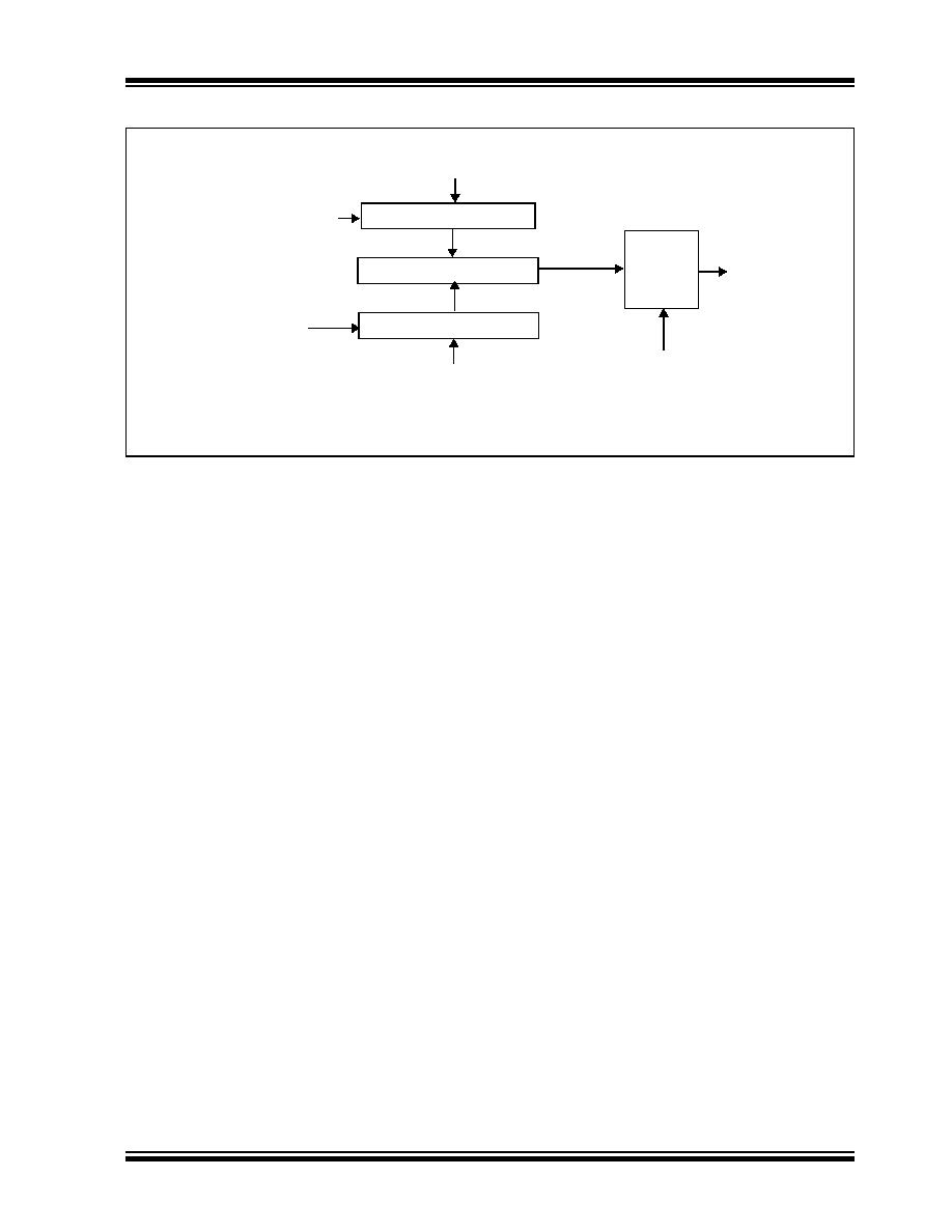
©
2006 Microchip Technology Inc.
Advance Information
DS70178A-page 133
dsPIC30F1010/202X
FIGURE 12-19:
PWM TRIGGER BLOCK DIAGRAM
12.19 PWM Interrupts
The PWM module can generate interrupts based on
internal timing or based on external signals via the cur-
rent-limit and Fault inputs. The primary time base mod-
ule can generate an interrupt request when a special
event occurs. Each PWM generator module has its
own interrupt request signal to the interrupt controller.
The interrupt for each PWM generator is an OR of the
trigger event interrupt request, the current-limit input
event, or the Fault input event for that module.
There are four interrupt request signals to the interrupt
control plus another interrupt request from the primary
time base on special events.
12.20 PWM Time Base Interrupts
The PWM module can generate interrupts based on
the primary time base and/or the individual time bases
in each PWM generator. The interrupt timing is speci-
fied by the Special Event Comparison Register
(SEVTCMP) for the primary time base, and by the
TRIGx registers for the individual time bases in the
PWM generator modules.
The primary time base special event interrupt is
enabled via the SEIEN bit in the PTCON register. The
individual time base interrupts generated by the trigger
logic in each PWM generator are controlled by the
TRGIEN bit in the PWMCONx registers.
12.21 PWM Fault and Current-Limit Pins
The PWM module supports multiple Fault pins for each
PWM generator. These pins are labeled SFLTx
(Shared Fault) or IFLTx (Individual Fault). The Shared
Fault pins can be seen and used by any of the PWM
generators. The Individual Fault pins are usable by
specific PWM generators.
Each PWM generator can have one pin for use as a
cycle-by-cycle current limit, and another pin for use as
either a cycle-by-cycle current limit or a latching current
Fault disable function.
12.22 Leading Edge Blanking
Each PWM generator supports "Leading Edge Blank-
ing" of the current-limit and Fault inputs via the
LEB<9:3> bits and the PHR, PHF, PLR, PLF, FLTLE-
BEN and CLLEBEN bits in the LEBCONx registers.
The purpose of leading edge blanking is to mask the
transients that occur on the application printed circuit
board when the power transistors are turned on and off.
The LEB bits support the blanking (ignoring) of the cur-
rent-limit and Fault inputs for a period of 0 to 1024 nsec
in 8.4 nsec increments following any specified rising or
falling edge of the coarse PWMH and PWML signals.
The coarse PWM signal (signal prior to the PWM fine
tuning) has resolution of 8.4 nsec (at 30 MIPS), which
is the same time resolution as the LEB counters.
The PHR, PHF, PLR and PLF bits select which edge of
the PWMH and PLWL signals will start the blanking
timer. If a new selected edge triggers the LEB timer
while the timer is still active from a previously selected
PWM edge, the timer reinitializes and continues
counting.
PTMRx
Compare Logic
4
15
Clk
=
TRIGx Register
TRGDIV<2:0>
Pulse
Divider
PWMx Trigger
15
4
PDI
PDI
TRIGx Write

dsPIC30F1010/202X
DS70178A-page 134
Advance Information
©
2006 Microchip Technology Inc.
The FLTLEBEN and CLLEBEN bits enable the applica-
tion of the blanking period to the selected Fault and
current-limit inputs.
The LEB duration @ 30 MIPS =
(LEB<9:3> + 1) / 120 MHz .
There is a blanking period offset of 8.4 nsec. Therefore
a LEB<9:3> value of zero yields an effective blanking
period of 8.4 ns.
If a current-limit or Fault inputs are active at the end of
the previous PWM cycle, and they are still active at the
start of the new PWM cycle and the dead time is non-
zero, the Fault or current limit will be detected
regardless of the LEB counter configuration.
12.23 PWM Fault Pins
Each PWM generator can select its own Fault input
source from a selection of up to 12 Fault/current-limit
pins. In the FCLCONx registers, each PWM generator
has control bits that specify the source for its Fault input
signal. These are the FLTSRC<3:0> bits. Additionally,
each PWM generator has a FLTIEN bit in the PWM-
CONx register that enables the generation of Fault
interrupt requests. Each PWM generator has an asso-
ciated Fault Polarity bit (FLTPOL) in the FCLCONx reg-
ister that selects the active level of the selected Fault
input.
The Fault pins actually serve two different purposes.
First is generation of Fault overrides for the PWM out-
puts. The action of overriding the PWM outputs and
generating an interrupt is performed asynchronously in
hardware so that Fault events can be managed quickly.
Second, the Fault pin inputs can be used to implement
either Current-Limit PWM mode or Current Force
mode.
PWM Fault condition states are available on the FLT-
STAT bit in the PWMCONx registers. The FLTSTAT bits
displays the Fault IRQ latch if the FIE bit is set. If Fault
interrupts are not enabled, then the FSTATx bits display
the status of the selected FLTx input in positive logic
format. When the Fault input pins are not used in asso-
ciation with a PWM generator, these pins become
general purpose I/O or interrupt input pins.
The FLTx pins are normally active high. The FLTPOL
bit in FCLCONx registers, if set to one, invert the
selected Fault input signal so that it is an active low.
The Fault pins are also readable through the PORT I/O
logic when the PWM module is enabled. This allows
the user to poll the state of the Fault pins in software.
12.23.1
FAULT INTERRUPTS
The FLTIENx bits in the PWMCONx registers deter-
mine if an interrupt will be generated when the FLTx
input is asserted high. The FLTMOD bits in the
FCLCONx register determines how the PWM genera-
tor and its outputs respond to the selected Fault input
pin. The FLTDAT<1:0> bits in the IOCONx registers
supply the data values to be assigned to the PWMxH,L
pins in the advent of a Fault.
The Fault pin logic can operate separately from the
PWM logic as an external interrupt pin. If the faults are
disabled from affecting the PWM generators in the
FCLCONx register, then the Fault pin can be used as a
general purpose interrupt pin.
12.23.2
FAULT STATES
The IOCONx register has two bits that determine the
state of each PWMx I/O pin when they are overridden
by a Fault input. When these bits are cleared, the
PWM I/O pin is driven to the inactive state. If the bit is
set, the PWM I/O pin is driven to the active state. The
active and inactive states are referenced to the polarity
defined for each PWM I/O pin (HPOL and LPOL
polarity control bits).
12.23.3
FAULT INPUT MODES
The Fault input pin has two modes of operation:
∑ Latched Mode: When the Fault pin is asserted,
the PWM outputs go to the states defined in the
FLTDAT bits in the IOCONx registers. The PWM
outputs remain in this state until the Fault pin is
deasserted AND the corresponding interrupt flag
has been cleared in software. When both of these
actions have occurred, the PWM outputs return to
normal operation at the beginning of the next
PWM cycle boundary. If the FLTSTAT bit is
cleared before the Fault condition ends, the PWM
module waits until the Fault pin is no longer
asserted to restore the outputs. Software can
clear the FLTSTAT bit by writing a zero to the
FLTIEN bit.
∑ Cycle-by-Cycle Mode: When the Fault input pin
is asserted, the PWM outputs remain in the deas-
serted PWM state for as long as the Fault pin is
asserted. For Complementary Output modes,
PWMH is low (deasserted) and PWML is high
(asserted). After the Fault pin is driven high, the
PWM outputs return to normal operation at the
beginning of the following PWM cycle.
The operating mode for each Fault input pin is selected
using the FLTMOD<1:0> control bits in the FCLCONx
register.
12.23.4
FAULT ENTRY
The response of the PWM pins to the Fault input pins
is always asynchronous with respect to the device
clock signals. That is, the PWM outputs should imme-
diately go to the states defined in the FLTDAT register
bits without any interaction from the dsPIC DSC device
or software.

©
2006 Microchip Technology Inc.
Advance Information
DS70178A-page 135
dsPIC30F1010/202X
Refer to Section 12.28 "Fault and Current-Limit
Override Issues with Dead-time Logic" for informa-
tion regarding data sensitivity and behavior in response
to current-limit or Fault events.
12.23.5
FAULT EXIT
The restoration of the PWM signals after a Fault condi-
tion has ended must occur at a PWM cycle boundary to
ensure proper synchronization of PWM signal edges
and manual signal overrides. The next PWM cycle
begins when the PTMRx value is zero.
12.23.6
FAULT EXIT WITH PTMR DISABLED
There is a special case for exiting a Fault condition
when the PWM time base is disabled (PTEN = 0).
When a Fault input is programmed for Cycle-by-Cycle
mode, the PWM outputs are immediately restored to
normal operation when the Fault input pin is deas-
serted. The PWM outputs should return to their default
programmed values. (The time base is disabled, so
there is no reason to wait for the beginning of the next
PWM cycle.)
When a Fault input is programmed for Latched mode,
the PWM outputs are restored immediately when the
Fault input pin is deasserted AND the FSTAT bit has
been cleared in software.
12.23.7
FAULT PIN SOFTWARE CONTROL
The Fault pin can be controlled manually in software.
Since the Fault input is shared with a PORT I/O pin, the
PORT pin can be configured as an output by clearing
the corresponding TRIS bit. When the PORT bit for the
pin is cleared, the Fault input will be activated.
12.24 PWM Current-Limit Pins
Each PWM generator can select its own current-limit
input source from up to12 current-limit/Fault pins. In the
FCLCONx registers, each PWM generator has control
bits (CLSRC<3:0>) that specify the source for its cur-
rent-limit input signal. Additionally, each PWM genera-
tor has a CLIEN bit in the PWMCONx register that
enables the generation of current-limit interrupt
requests. Each PWM generator has an associated
Fault polarity bit CLPOL in the FCLCONx register.
The current-limit pins actually serve two different pur-
poses. They can be used to implement either Current-
Limit PWM mode or Current Reset PWM mode.
1.
When the CLIEN bit is set in the PWMCONx
registers, the PWMxH,L outputs are forced to
the values specified by the CLDAT<1:0> bits in
the IOCONx register, if the selected current-limit
input signal is asserted.
2.
When the CLMOD bit is zero AND the XPRES
bit in the PWMCONx register is `
01
' AND the
PWM generator is in Independent Time Base
mode (
ITB = 1
), then a current-limit signal
resets the time base for the affected PWM gen-
erator. This behavior is called Current Reset
mode, which is used in some Power Factor
Correction (PFC) applications.
12.24.1
CURRENT-LIMIT INTERRUPTS
The state of the PWM current-limit conditions is avail-
able on the CLSTAT bits in the PWMCONx registers.
The CLSTAT bits display the current-limit IRQ flag if
the CLIEN bit is set. If current-limit interrupts are not
enabled, then the CLSTAT bits display the status of the
selected current-limit inputs in positive logic format.
When the current-limit input pin associated with a
PWM generator is not used, these pins become
general purpose I/O or interrupt input pins.
The current-limit pins are normally active high. If set to
`
1
', the CLPOL bit in FCLCONx registers inverts the
selected current-limit input signal to active high.
The interrupts generated by the selected current-limit
signals are combined to create a single interrupt
request signal to the interrupt controller, which has its
own interrupt vector, interrupt flag bit, interrupt enable
bit and interrupt priority bits associated with it.
The Fault pins are also readable through the PORT I/O
logic when the PWM module is enabled. This allows
the user to poll the state of the Fault pins in software.
12.25 Simultaneous PWM Faults and
Current Limits
The current-limit override function, if enabled and
active, forces the PWMxH,L pins to the values speci-
fied by the CLDAT<1:0> bits in the IOCONx registers
UNLESS the Fault function is enabled and active. If the
selected Fault input is active, the PWMxH,L outputs
assume the values specified by the FLTDAT<1:0> bits
in the IOCONx registers.
12.26 PWM Fault and Current-Limit TRG
Outputs To ADC
The Fault and current-limit source selection fields in the
FCLCONx registers (FLTSRC<3:0> and CLSRC<3:0>)
control multiplexers in each PWM generator module.
The control multiplexers select the desired Fault and
current-limit signals for their respective modules. The
selected Fault and current-limit signals are also avail-
able to the ADC module as trigger signals that initiate
ADC sampling and conversion operations.
Note:
The user should use caution when control-
ling the Fault inputs in software. If the
TRIS bit for the Fault pin is cleared and the
PORT bit is set high, then the Fault input
cannot be driven externally.

dsPIC30F1010/202X
DS70178A-page 136
Advance Information
©
2006 Microchip Technology Inc.
12.27 PWM Output Override Priority
If the PWM module is enabled, the priority of PWMx pin
ownership is:
1.
PWM Generator (lowest priority)
2.
Output Override
3.
Current-Limit Override
4.
Fault Override
5.
PENx (GPIO/PWM) ownership (highest priority)
If the PWM module is disabled, the GPIO module
controls the PWMx pins.
12.28 Fault and Current-Limit Override
Issues with Dead-time Logic
The PWMxH and PWMxL outputs are immediately
driven low (deasserted) as specified by the
CLDAT<1:0> and the FLTDAT<1:0> bits when a
current-limit or a Fault event occurs.
The override data is gated with the PWM signals going
into the dead-time logic block, and at the output of the
PWM module, just ahead of the PWM pin output
buffers.
Many applications require fast response to current
shutdown for accurate current control and/or to limit
circuitry damage to Fault currents.
Some applications will set the complementary
PWM outputs high in synchronous rectifier
designs when a Fault or current-limit event
occurs. If the CLDAT or FLTDAT bits are set to `
1
',
and their associated event occurs, then these
asserted outputs will be delayed by clocked logic
in the
dead-time circuitry.
12.29 Asserting Outputs via Current
Limit
It is possible to use the CLDAT bits to assert the
PWMxH,L outputs in response to a current-limit event.
Such behavior could be used as a current "force" fea-
ture in response to an external current or voltage mea-
surement that indicates a sudden sharp increase in the
load on the power-converter output. Forcing the PWM
"ON" could be viewed as a "Feed-Forward" term that
allows quick system response to unexpected load
increases without waiting for the digital control loop to
respond.
12.30 PWM Immediate Update
For high-performance PWM control-loop applications,
the user may want to force the duty cycle updates to
occur immediately. Setting the IUE bit in the
PWMCONx register enables this feature.
In a closed-loop control application, any delay between
the sensing of a system's state and the subsequent
outputting of PWM control signals that drive the appli-
cation reduces the loop stability. Setting the IUE bit
minimizes the delay between writing the duty cycle reg-
isters and the response of the PWM generators to that
change.
12.31 PWM Output Override
All control bits associated with the PWM output
override function are contained in the IOCONx register.
If the PENH, PENL bits are reset (default state), then
the PWM module controls the PWMx output pins.
The PWM output override bits allow the user to manu-
ally drive the PWM I/O pins to specified logic states
independent of the duty cycle comparison units.
The OVRDAT<1:0> bits in the IOCONx register deter-
mine the state of the PWM I/O pins when a particular
output is overridden via the OVRENH,L bits.
The OVRENH, OVRENL bits are active high control
bits. When the OVREN bits are set, the corresponding
OVRDAT bit overrides the PWM output from the PWM
generator.
12.31.1
COMPLEMENTARY OUTPUT MODE
When the PWM is in Complementary Output mode, the
dead-time generator is still active with overrides. The
output overrides and Fault overrides generate control
signals used by the dead-time unit to set the outputs as
requested, including dead time.
Dead-time insertion can be performed when PWM
channels are overridden manually.
12.31.2
OVERRIDE SYNCHRONIZATION
If the OSYNC bit in the IOCONx register is set, the out-
put overrides performed via the OVRENH,L and the
OVDDAT<1:0> bits are synchronized to the PWM time
base. Synchronous output overrides occur when the
time base is zero.
If PTEN =
0
, meaning the timer is not running, writes to
IOCON take effect on the next T
CY
boundary.
12.32 Functional Exceptions
12.32.1
POWER RESET CONDITIONS
All registers associated with the PWM module are reset
to the states given in Table 12-4 upon a Power-on
Reset. On a device reset, the PWM output pins are
tri-stated.
12.32.2
SLEEP MODE
The selected Fault input pin has the ability to wake the
CPU from Sleep mode. The PWM module should gen-
erate an asynchronous interrupt if any of the selected
Fault pins is driven low while in Sleep.
It is recommended that the user disable the PWM out-
puts prior to entering Sleep mode. If the PWM module
is controlling a power conversion application, the action

©
2006 Microchip Technology Inc.
Advance Information
DS70178A-page 137
dsPIC30F1010/202X
of putting the device into Sleep will cause any control
loops to be disabled, and most applications will likely
experience issues unless they are explicitly designed
to operate in an Open-Loop mode.
12.32.3
CPU IDLE MODE
The dsPIC30F1010/202X module has a PTSIDL con-
trol bit in the PTCON register. This bit determines if the
PWM module continues to operate or stops when the
device enters Idle mode. Stopped Idle mode functions
like Sleep mode, and Fault pins are asynchronously
active.
∑
PTSIDL = 1
(Stop module when in Idle mode)
∑
PTSIDL = 0
(Don't stop module when in Idle
mode)
It is recommended that the user disable the PWM out-
puts prior to entering Idle mode. If the PWM module is
controlling a power-conversion application, the action
of putting the device into Idle will cause any control
loops to be disabled, and most applications will likely
experience issues unless they are explicitly designed
to operate in an Open-Loop mode.
12.33 Register Bit Alignment
Table 12-4 on page 143 shows the registers for the
SMPS PWM module. All time-based data for the mod-
ule is always bit-aligned with respect to time. For exam-
ple: bit 3 in the period register, the duty cycle registers,
the dead-time registers, the trigger registers and the
phase registers always represents a value of 18.4
nsec, assuming 30 MIPS operation. Unused portions of
registers always read as zeros.
The use of data alignment makes it easier to write soft-
ware because it eliminates the need to shift time values
to fit into registers. It also eases the computation and
understanding of time allotment within a PWM cycle.
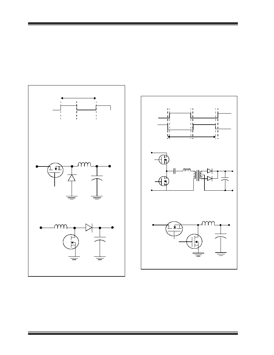
dsPIC30F1010/202X
DS70178A-page 138
Advance Information
©
2006 Microchip Technology Inc.
12.34 APPLICATION EXAMPLES:
12.34.1 STANDARD PWM MODE
In standard PWM mode, the PWM output is typically
connected to a single transistor, which charges an
inductor, as shown in Figure 12-20. Buck and Boost
converters typically use standard PWM mode.
FIGURE 12-20:
APPLICATIONS OF
STANDARD PWM MODE
12.34.2 APPLICATION OF COMPLEMENTARY
PWM MODE
Complementary mode PWM is often used in circuits
that use two transistors in a bridge configuration where
transformers are not used, as shown in Figure 12-21.
If transformers are used, then some means must be
provided to ensure that no net DC currents flow
through the transformer to prevent core saturation.
FIGURE 12-21:
APPLICATIONS OF
COMPLEMENTARY PWM
MODE
Buck Converter
+V
IN
L1
PWM1H
+
V
OUT
Boost Converter
+V
IN
PWM1H
L1
V
OUT
+
Period
PWM1H
T
ON
T
OFF
Inductor charges during T
ON
T
ON
versus Period controls power flow
V
OUT
L1
+V
IN
PWM1H
PWM1L
Synchronous Buck Converter
+
+
+V
IN
PWM1H
PWM1L
C
R
T1
Series Resonant Half Bridge Converter
L
R
V
OUT
PWM1L
PWM1H
Dead Time
Dead Time
Dead Time
Period

©
2006 Microchip Technology Inc.
Advance Information
DS70178A-page 139
dsPIC30F1010/202X
12.34.3 APPLICATION OF PUSH-PULL PWM
MODE
Push-Pull PWM mode is typically used in transformer
coupled circuits to ensure that no net DC currents flow
through the transformer. Push-Pull mode ensures that
the same duty cycle PWM pulse is applied to the
transformer windings in alternate directions, as shown
in Figure 12-22.
FIGURE 12-22:
APPLICATIONS OF PUSH-
PULL PWM MODE
12.34.4 APPLICATION OF MULTI-PHASE PWM
MODE
Multi-Phase PWM mode is often used in DC/DC con-
verters that must handle very fast load current tran-
sients and fit into tight spaces. A multi-phase converter
is essentially a parallel array of buck converters that
are operated slightly out of phase of each other, as
shown in Figure 12-23. The multiple phases create an
effective switching speed equal to the sum of the indi-
vidual converters. If a single phase is operating with a
333 KHz PWM frequency, then the effective switching
frequency for the circuit is 1 MHz. This high switching
frequency greatly reduces output capacitor size
requirements and improves load transient response.
FIGURE 12-23:
APPLICATIONS OF MULTI-
PHASE PWM MODE
+
T1
V
OUT
Half Bridge Converter
+V
IN
PWM1H
PWM1L
+
+
L1
PWM1H
PWM1L
T
ON
T
OFF
T
ON
T
OFF
Period
Period
Dead Time
Dead Time
Dead Time
T1
+
+V
IN
PWM1H
PWM1L
Push-Pull Buck Converter
L1
V
OUT
PWH1H
PWH1L
PWH1L
PWH1H
+V
IN
T1
L1
V
OUT
Full Bridge Converter
+
+
+
V
IN
PWM1H
PWM2H
PWM3H
L1
L2
L3
PWM1L
PWM1L
PWM1L
V
OUT
Converter
Multiphase DC/DC
PWM1H
PWM1L
PWM2H
PWM2L
PWM3H
PWM3L
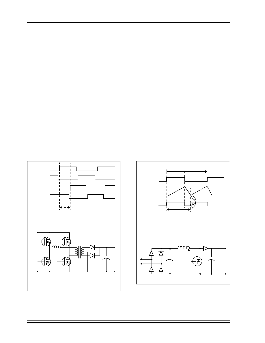
dsPIC30F1010/202X
DS70178A-page 140
Advance Information
©
2006 Microchip Technology Inc.
12.34.5 APPLICATION OF VARIABLE PHASE PWM
MODE
Variable phase PWM is used in newer power conver-
sion topologies that are designed to reduce switching
losses. In standard PWM methods, any time a transis-
tor switches between the conducting state and the
nonconducting state (and vice versa), the transistor is
exposed to the full current and voltage condition for
the period of time it takes the transistor to turn on or
off. The power loss (V * I * Tsw * FPWM) becomes
appreciable at high frequencies. The Zero Voltage
Switching (ZVS) and Zero Current Switching (ZVC) cir-
cuit topologies attempt to use quasi-resonant tech-
niques to shift either the voltage or current waveforms
relative to each other. This action either makes the
voltage or the current zero at the time the transistor
turns on or off. If either the current or the voltage is
zero, then there is no switching loss generated.
In variable phase PWM modes, the duty cycle is fixed
at 50%, and the power flow is controlled by varying the
phase relationship between the PWM channels, as
shown in Figure 12-24.
FIGURE 12-24:
APPLICATION OF
VARIABLE PHASE PWM
MODE
12.34.6 APPLICATION OF CURRENT RESET PWM
MODE
In Current Reset PWM mode, the PWM frequency var-
ies with the load current. This mode is different than
most PWM modes because the user sets the maxi-
mum PWM period, but an external circuit measures
the inductor current. When the inductor current falls
below a specified value, the external current compara-
tor circuit generates a signal that resets the PWM time
base counter. The user specifies a PWM "on" time,
and then some time after the PWM signal becomes
inactive, the inductor current falls below a specified
value and the PWM counter is reset earlier than the
programmed PWM period. This mode is sometimes
called Constant On-Time.
This mode should not be confused with cycle-by-cycle
current-limiting PWM, where the PWM is asserted, an
external circuit generates a current Fault and the PWM
signal is turned off before its programmed duty cycle
would normally turn it off. In this mode, shown in
Figure 12-25, the PWM frequency is fixed per the time
base period.
FIGURE 12-25:
APPLICATION OF
CURRENT RESET PWM
MODE
PWM1H
PWM1L
PWM2H
PWM2L
Variable Phase Shift
+
Full Bridge ZVT Converter
T1
V
OUT
+V
IN
PWM1H
PWM1H
PWM1H
PWM1H
+
+
AC
IN
C
IN
L
I
L
PWM1H
D
V
OUT
C
OUT
External current comparator resets PWM counter
PWM cycle restarts early
This is a variable frequency PWM mode
PWM1H
PWM1H
I
L
T
ON
T
OFF
Actual Period
Programmed Period

©
2006 Microchip Technology Inc.
Advance Information
DS70178A-page 141
dsPIC30F1010/202X
12.35 METHODS TO REDUCE EMI
The goal is to move the PWM edges around in time to
spread the EMI energy over a range of frequencies to
reduce the peak energy at any given frequency during
the EMI measurement process, which measures long
term averages.
The EMI measurement process integrates the EMI
energy into 9 kHz wide frequency bins. Assuming that
the carrier (PWM) frequency is 150 kHz, a 6% dither
will yield a 9 kHz wide dither.
12.35.1 METHOD #1: PROGRAMMABLE FRC
DITHER
This method dithers all of the PWM outputs and the
system clock. The advantage of this method is that no
CPU resources are required. It is automatic once it is
setup. The user can periodically update these values
to simulate a more random frequency pattern.
12.35.2 METHOD #2: SOFTWARE CONTROLLED
DITHER
This method uses software to dither individual PWM
channels by scaling the duty cycle and period. This
method consumes CPU resources:
Assume:
4 PWM channels updated @ 150 kHz rate:
600 kHz x (5 clocks (2 mul, 1 tblrdl, 1 mov))
= 3 MIPS additional work load
12.35.3 METHOD #3: SOFTWARE SCALING OF
TIME BASE PERIOD
This method used software to scale just the time base
period. Assuming that the dither rate is relatively slow
(about 250 Hz), the application control loop should be
able to compensate for the changes in PWM period
and adjust the duty cycle accordingly.
12.35.4 METHOD #4: FREQUENCY MODULATION
This method varies the frequency at which the PWM
cycle is varied (dithered). The frequency modulation
process is similar (mathematically speaking) to Phase
Modulation when analyzed over a small time window.
The PWM module has the capability to phase modu-
late the PWM signals via the phase offset registers.
Phase modulation has the advantage that the software
is simpler and faster because multiple multiply opera-
tions (used for dithering frequency by scaling period
and duty cycles) are replaced with fewer additions or
simple updates of phase offset
values into the phase registers.
This method also has these advantages:
1.
Multi-phase and variable phase PWM modes
could still be created.
2.
The PWM generators can still use the common
time base, which simplifies determining when a
"quiet time" is available for measuring current.
This method has one disadvantage: the phase modu-
lation has to be at a relatively high update rate to
achieve usable frequency spreading.
12.35.5 INDEPENDENT PWM CHANNEL
DITHERING ISSUES:
Issues for multi-phase or variable phase designs using
independent output dithering must consider these
issues:
1.
The phases are no longer phase aligned.
2.
Control of current sharing among phases is
more difficult.

dsPIC30F1010/202X
DS70178A-page 142
Advance Information
©
2006 Microchip Technology Inc.
12.36 EXTERNAL SYNCHRONIZATION
FEATURES
In large power conversion systems, it is often desir-
able to be able to synchronize multiple power control-
lers to ensure that "beat frequencies" are not
generated within the system, or as a means to ensure
"quiet" periods during which current and voltage mea-
surements can be made.
dsPIC30F202X devices (excluding 28-pin packages)
have input and/or output pins that provide the capabil-
ity to either synchronize the SMPS dsPIC DSC device
with an external device or have external devices syn-
chronized to the SMPS dsPIC DSC. These synchro-
nizing features are enabled via the SYNCIEN and
SYNCOEN bits in the PTCON control register in the
PWM module.
The SYNCPOL bit in the PTCON register selects
whether the rising edge or the falling edge of the
SYNCI signal is the active edge. The SYNCPOL bit in
the PTCON register also selects whether the SYNCO
output pulse is low active or high active.
The SYNCSRC<2:0> bits in the PTCON register
specify the source for the SYNCI signal.
If the SYNCI feature is enabled, the primary time base
counter is reset when an active SYNCI edge is
detected. If the SYNCO feature is enabled, an output
pulse is generated when the primary time base
counter rolls over at the end of a PWM cycle.
The recommended SYNCI pulse width should be more
than 100 nsec. The expected SYNCO output pulse
width will be approximately 100 nsec.
When using the SYNCI feature, it is recommended
that the user program the period register with a period
value that is slightly longer than the expected period of
the external synchronization input signal. This pro-
vides protection in case the SYNCI signal is not
received due to noise or external component failure.
With a reasonable period value programmed into the
PERIOD register, the local power conversion process
should remain operational even if the global
synchronization signal is not received.
12.37 TIMING EXTERNAL PWM
TRIGGER EVENTS
The TRGCONx control registers provide the capability
to capture the time base value of an individual PWM
generator at the moment a selected external trigger
signal is detected. This timing information is useful in
many applications where external circuitry is monitor-
ing current or voltage. The software may want to deter-
mine if the external trigger event occurred either too
early or too late.
12.38 CPU LOAD STAGGERING
The SMPS dsPIC DSC has the ability to stagger the
individual trigger comparison operations. This feature
helps to level the processor's workload to minimize
situations where the processor is overloaded.
Assume a situation where there are four PWM chan-
nels controlling four independent voltage outputs.
Assume further that each PWM generator is operating
at 1000 kHz (1 µsec period) and each control loop is
operating at 125 kHz (8 µsec).
The TDIV<2:0> bits in each PWMCONx register will
be set to `
111
', which selects that every 8th trigger
comparison match will generate a trigger signal to the
ADC to capture data and begin a conversion process.
If the stagger-in-time feature did not exist, all of the
requests from all of the PWM trigger registers might
occur at the same time. If this "pile-up" were to hap-
pen, some data sample might become stale (outdated)
by the time the data for all four channels can be
processed.
With the stagger-in-time feature, the trigger signals are
spaced out over time (during succeeding PWM peri-
ods) so that all of the data is processed in an orderly
manner.
The ROLL counter is a counter connected to the pri-
mary time base counter. The ROLL counter is incre-
mented each time the primary time base counter
reaches terminal count (period rollover).
The stagger-in-time feature is controlled by the
TRGSTRT<5:0> bits in the TRGCONx registers. The
TRGSTRT<5:0> bits specify the count value of the
ROLL counter that must be matched before an individ-
ual trigger comparison module in each of the PWM
generators can begin to count the trigger comparison
events as specified by the TRGDIV<2:0> bits in the
PWMCONx registers.
So, in our example with the four PWM generators, the
first PWM's TRGSTRT<5:0> bits would be `
000
', the
second PWM's TRGSTRT bits would be set to `
010
',
the third PWM's TRGSTRT bits would be set to `
100
'
and the fourth PWM's TRGSTRT bits would be set to
`
110
'. Therefore, over a total of eight PWM cycles, the
four separate control loops could be run each with
their own 2-µsec time period.
12.39 EXTERNAL TRIGGER BLANKING
Using the LEB<9:3> bits in the LEBCONx registers,
the PWM module has the capability to blank (ignore)
the external current and Fault inputs for a period of 0
to 1024 nsec. This feature is useful if power transistor
turn-on induced transients make current sensing
difficult at the start of a PWM cycle.

©
2006 Microchip Technology Inc.
Advance Information
DS70178A-page 143
dsPIC30F1010/202X
T
A
B
L
E
12
-4
:
S
MP
S PW
M R
E
GI
STE
R
M
A
P
F
ile
Na
m
e
ADR
B
it
1
5
Bit
1
4
Bit
1
3
Bit
1
2
B
i
t
1
1
Bit
1
0
Bit
9
B
i
t
8
B
it 7
B
it
6
B
it 5
B
it 4
B
it 3
B
it
2
B
it 1
B
it
0
A
ll
Re
se
t
s
PTC
O
N
0
4
0
0
P
TE
N
--
P
T
S
I
D
L
S
E
S
T
A
T
SEI
EN
EI
PU
SYNCPO
L
SYNCO
EN
SY
N
C
E
N
SYNCSRC<2
:
0
>
SEVT
PS<3
:
0
>
0
0
0
0
P
T
PER
0
4
0
2
P
T
PER<1
5
:
3
>
--
--
--
FFF
0
MD
C
0
4
0
4
M
DC<
1
5
:0
>
0
000
SE
VTCM
P
0
4
0
6
SEV
TCM
P
<1
5
:
3
>
--
--
--
0
000
PWM
C
ON
1
0
4
0
8
F
L
T
S
T
A
T
CL
S
T
A
T
T
R
G
S
T
A
T
F
L
T
IEN
C
L
I
EN
T
R
G
I
EN
IT
B
M
DCS
DT
C<1
:
0
>
--
--
--
--
X
PRES
I
U
E
0
0
0
0
IOCO
N
1
0
4
0
A
P
E
N
H
P
E
N
L
P
OLH
P
OL
L
P
M
O
D<1:
0>
OV
RE
NH
O
V
RE
NL
OV
RDA
T
<
1:0>
F
L
T
D
A
T
<1:0
>
C
L
D
A
T
<1:0
>
--
O
SYNC
0
0
0
0
FC
L
C
ON
1
0
40C
--
--
--
C
LS
R
C
<
3:
0>
C
L
P
O
L
C
LM
OD
FL
T
S
R
C
<
3:
0>
FL
T
P
OL
FL
T
M
OD
<
1
:0
>
0
000
P
D
C
1
04
0E
PDC1
<1
5
:
0
>
0
000
PHAS
E1
0
4
1
0
P
H
ASE1
<1
5
:
2
>
--
--
0
000
DT
R1
0
4
1
2
--
--D
T
R
1
<
1
3
:
2
>
--
--
0
000
AL
T
D
TR1
0
4
1
4
--
--
A
L
T
DT
R1
<1
3
:
2
>
--
--
0
000
T
R
I
G
1
0
4
1
6
T
RIG<1
5
:3
>
--
--
--
0
000
T
R
G
C
ON1
0
4
1
8
T
RGDI
V
<
2
:
0
>
---
---
---
---
---
---
---
TR
G
S
TR
T
<
5:0
>
0
000
L
EBCO
N
1
0
4
1
A
P
H
R
PHF
P
L
R
PL
F
F
L
T
L
EBEN
CL
L
EBE
N
L
EB
<9
:
3
>
--
--
--
0
000
PWM
C
ON
2
0
4
1
C
F
L
T
S
T
A
T
C
L
S
T
A
T
T
RG
S
T
A
T
F
L
T
I
EN
CL
IEN
T
RG
IEN
I
T
B
M
DCS
DT
C<1
:
0
>
--
--
--
--
X
PRES
I
U
E
0
0
0
0
IOCO
N
2
0
4
1
E
P
E
N
H
P
E
N
L
P
OLH
P
OL
L
P
M
O
D<1:
0>
OV
RE
NH
O
V
RE
NL
OV
RDA
T
<
1:0>
F
L
T
D
A
T
<1:0
>
C
L
D
A
T
<1:0
>
--
O
SYNC
0
0
0
0
F
C
LC
O
N
2
0
42
0
--
--
--
C
LS
R
C
<
3:
0>
C
L
P
O
L
C
LM
OD
FL
T
S
R
C
<
3:
0>
FL
T
P
OL
FL
T
M
OD
<
1
:0
>
0
000
P
D
C
2
04
22
PDC2
<1
5
:
0
>
0
000
PHAS
E2
0
4
2
4
P
H
ASE2
<1
5
:
2
>
--
--
0
000
DT
R2
0
4
2
6
--
--D
T
R
2
<
1
3
:
2
>
--
--
0
000
AL
T
D
TR2
0
4
2
8
--
--
A
L
T
DT
R2
<1
3
:
2
>
--
--
0
000
T
R
I
G
2
0
4
2
A
T
RIG<1
5
:3
>
--
--
--
0
000
T
R
G
C
ON2
0
42C
T
R
GDI
V
<2
:0>
---
---
---
---
---
---
---
TR
G
S
TR
T
<
5:0
>
0
000
L
EBCO
N
2
0
4
2
E
P
H
R
PHF
P
L
R
PL
F
F
L
T
L
EBEN
CL
L
EBE
N
L
EB
<9
:
3
>
--
--
--
0
000
PWM
C
ON
3
0
4
3
0
F
L
T
S
T
A
T
CL
S
T
A
T
T
R
G
S
T
A
T
F
L
T
IEN
C
L
I
EN
T
R
G
I
EN
IT
B
M
DCS
DT
C<1
:
0
>
--
--
--
--
X
PRES
I
U
E
0
0
0
0
IOCO
N
3
0
4
3
2
P
E
N
H
P
E
N
L
P
OLH
P
OL
L
P
M
O
D<1:
0>
OV
RE
NH
O
V
RE
NL
OV
RDA
T
<
1:0>
F
L
T
D
A
T
<1:0
>
C
L
D
A
T
<1:0
>
--
O
SYNC
0
0
0
0
F
C
LC
O
N
3
0
43
4
--
--
--
C
LS
R
C
<
3:
0>
C
L
P
O
L
C
LM
OD
FL
T
S
R
C
<
3:
0>
FL
T
P
OL
FL
T
M
OD
<
1
:0
>
0
000
P
D
C
3
04
36
PDC3
<1
5
:
0
>
0
000
PHAS
E3
0
4
3
8
P
H
ASE3
<1
5
:
2
>
--
--
0
000
DT
R3
0
4
3
A
--
--D
T
R
3
<
1
3
:
2
>
--
--
0
000
A
L
TD
T
R
3
0
43C
--
--
A
L
T
DT
R3
<1
3
:
2
>
--
--
0
000
T
R
I
G
3
0
4
3
E
T
RIG<1
5
:3
>
--
--
--
0
000
T
R
G
C
ON3
0
4
4
0
T
RGDI
V
<
2
:
0
>
---
---
---
---
---
---
---
TR
G
S
TR
T
<
5:0
>
0
000
L
EBCO
N
3
0
4
4
2
P
H
R
PHF
P
L
R
PL
F
F
L
T
L
EBEN
CL
L
EBE
N
L
EB
<9
:
3
>
--
--
--
0
000
P
W
MCON
4
0
4
4
4
F
L
T
S
T
A
T
CL
S
T
A
T
T
R
G
S
T
A
T
F
L
T
IE
N
C
L
I
E
N
T
R
G
I
E
N
IT
B
M
DCS
DT
C<1
:
0>
T
R
G
D
IV
<2:0
>
T
RGM
O
D
X
P
R
E
S
IUE
0
000
IOCO
N
4
0
4
4
6
P
E
N
H
P
E
N
L
P
OLH
P
OL
L
P
M
O
D<1:
0>
OV
RE
NH
O
V
RE
NL
OV
RDA
T
<
1:0>
F
L
T
D
A
T
<1:0
>
C
L
D
A
T
<1:0
>
--
O
SYNC
0
0
0
0
dsPIC30F1010/202X
DS70178A-page 144
Advance Information
©
2006 Microchip Technology Inc.
F
C
LC
O
N
4
0
44
8
--
--
--
C
LS
R
C
<
3:
0>
C
L
P
O
L
C
LM
OD
E
F
L
T
S
R
C
<
3:
0>
FL
T
P
OL
FL
T
M
OD
<
1
:0
>
0
000
P
D
C
4
04
4A
PDC4
<
1
5
:
0
>
0
000
PHAS
E4
0
4
4
C
P
H
ASE4
<1
5
:
2
>
--
--
0
000
DT
R4
0
4
4
E
--
--
DT
R4
<1
3
:
2
>
--
--
0
000
AL
T
D
TR4
0
4
5
0
--
--
A
L
T
DT
R4
<1
3
:
2
>
--
--
0
000
T
R
I
G
4
0
4
5
2
T
RIG<1
5
:3
>
--
--
--
0
000
T
R
G
C
ON4
0
4
5
4
T
RGDI
V
<
2
:
0
>
---
---
---
---
---
---
---
TR
G
S
TR
T
<
5:0
>
0
000
L
EBCO
N
4
0
4
5
6
P
H
R
PHF
P
L
R
PL
F
F
L
T
L
EBEN
CL
L
EBE
N
L
EB
<9
:
3
>
--
--
--
0
000
R
e
s
e
r
v
ed
04
5
8
-
47F
--
--
--
--
--
--
--
--
--
--
--
--
--
--
--
--
0
000
T
A
BLE
1
2
-4:
S
M
P
S
P
W
M
RE
GIS
T
E
R
MAP
(CONTINUE
D)

©
2006 Microchip Technology Inc.
Advance Information
DS70178A-page 145
dsPIC30F1010/202X
13.0
SPI MODULE
The Serial Peripheral Interface (SPI) module is a syn-
chronous serial interface. It is useful for communicating
with other peripheral devices such as EEPROMs, shift
registers, display drivers and A/D converters, or other
microcontrollers. It is compatible with Motorola's SPI
and SIOP interfaces.
13.1
Operating Function Description
Each SPI module consists of a 16-bit shift register,
SPIxSR (where x = 1 or 2), used for shifting data in
and out, and a buffer register, SPIxBUF. A control reg-
ister, SPIxCON, configures the module. Additionally, a
Status register, SPIxSTAT, indicates various status
conditions.
The serial interface consists of 4 pins: SDIx (serial
data input), SDOx (serial data output), SCKx (shift
clock input or output), and SSx (active low slave
select).
In Master mode operation, SCK is a clock output, but
in Slave mode, it is a clock input.
A series of eight (8) or sixteen (16) clock pulses shifts
out bits from the SPIxSR to SDOx pin and simulta-
neously shifts in data from SDIx pin. An interrupt is
generated when the transfer is complete and the cor-
responding interrupt flag bit (SPI1IF or SPI2IF) is set.
This interrupt can be disabled through an interrupt
enable bit (SPI1IE or SPI2IE).
The receive operation is double-buffered. When a
complete byte is received, it is transferred from
SPIxSR to SPIxBUF.
If the receive buffer is full when new data is being
transferred from SPIxSR to SPIxBUF, the module will
set the SPIROV bit, indicating an Overflow condition.
The transfer of the data from SPIxSR to SPIxBUF will
not be completed and the new data will be lost. The
module will not respond to SCL transitions while
SPIROV is
1
, effectively disabling the module until
SPIxBUF is read by user software.
Transmit writes are also double-buffered. The user
writes to SPIxBUF. When the master or slave transfer
is completed, the contents of the shift register
(SPIxSR) is moved to the receive buffer. If any trans-
mit data has been written to the buffer register, the
contents of the transmit buffer are moved to SPIxSR.
The received data is thus placed in SPIxBUF and the
transmit data in SPIxSR is ready for the next transfer.
In Master mode, the clock is generated by prescaling
the system clock. Data is transmitted as soon as a
value is written to SPIxBUF. The interrupt is generated
at the middle of the transfer of the last bit.
In Slave mode, data is transmitted and received as
external clock pulses appear on SCK. Again, the inter-
rupt is generated when the last bit is latched. If SSx
control is enabled, then transmission and reception
are enabled only when SSx = low. The SDOx output
will be disabled in SSx mode with SSx high.
The clock provided to the module is (F
OSC
/ 2). This
clock is then prescaled by the primary (PPRE<1:0>)
and the secondary (SPRE<2:0>) prescale factors. The
CKE bit determines whether transmit occurs on transi-
tion from active clock state to Idle clock state, or vice
versa. The CKP bit selects the Idle state (high or low)
for the clock.
13.1.1
WORD AND BYTE
COMMUNICATION
A control bit, MODE16 (SPIxCON<10>), allows the
module to communicate in either 16-bit or 8-bit mode.
16-bit operation is identical to 8-bit operation, except
that the number of bits transmitted is 16 instead of 8.
The user software must disable the module prior to
changing the MODE16 bit. The SPI module is reset
when the MODE16 bit is changed by the user.
A basic difference between 8-bit and 16-bit operation is
that the data is transmitted out of bit 7 of the SPIxSR for
8-bit operation, and data is transmitted out of bit 15 of
the SPIxSR for 16-bit operation. In both modes, data is
shifted into bit 0 of the SPIxSR.
13.1.2
SDOx DISABLE
A control bit, DISSDO, is provided to the SPIxCON reg-
ister to allow the SDOx output to be disabled. This will
allow the SPI module to be connected in an input only
configuration. SDO can also be used for general
purpose I/O.
Note: This data sheet summarizes features of this group
of dsPIC30F devices and is not intended to be a complete
reference source. For more information on the CPU,
peripherals, register descriptions and general device
functionality, refer to the "dsPIC30F Family Reference
Manual" (DS70046).
Note:
The dsPIC30F1010/202X family has only
one SPI module. All references to x = 2 are
intended for software compatibility with
other dsPIC DSC devices.
Note:
If the module is used in a transmit only
configuration, the user application must
perform a read of the SPxBUF to avoid a
receive Overflow condition (
SPIROV = 1
).
Note:
Both the transmit buffer (SPIxTXB) and
the receive buffer (SPIxRXB) are mapped
to the same register address, SPIxBUF.
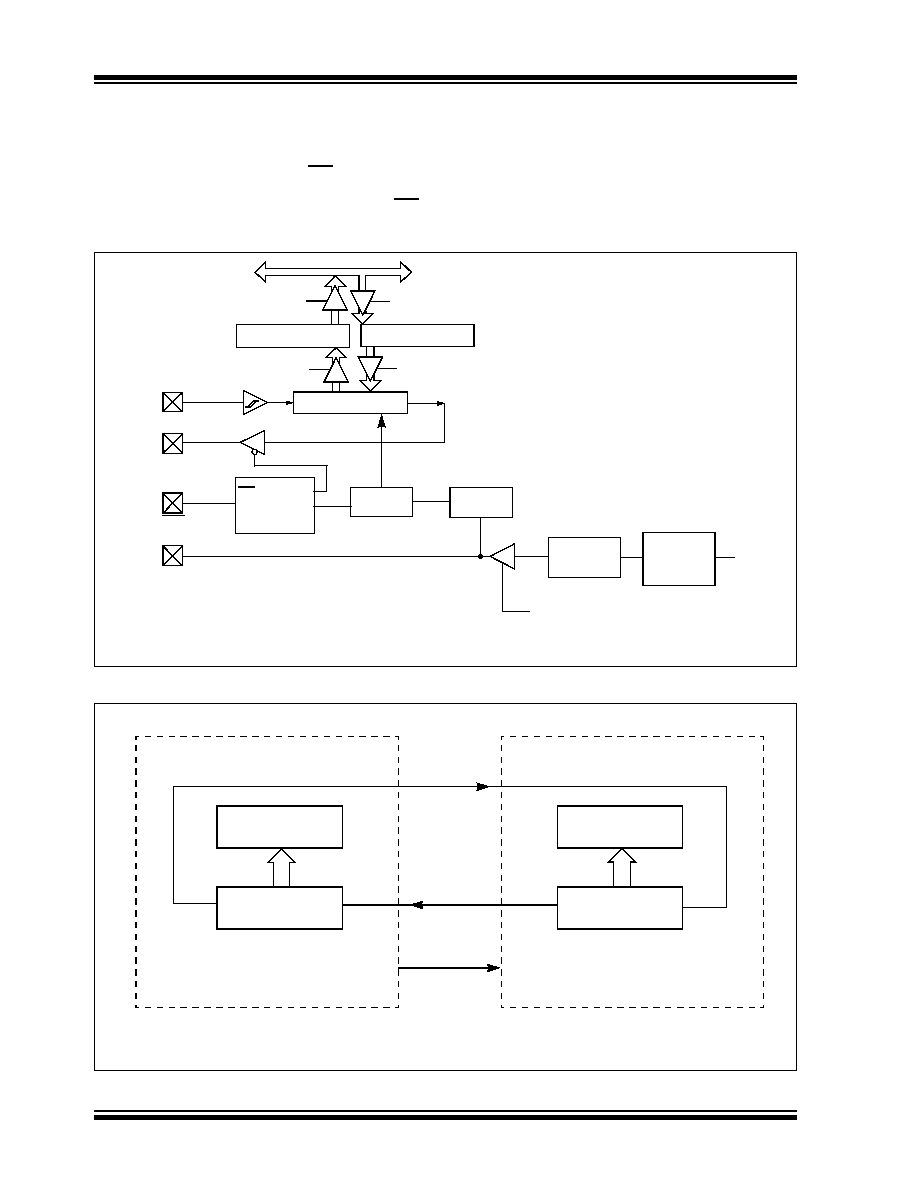
dsPIC30F1010/202X
DS70178A-page 146
Advance Information
©
2006 Microchip Technology Inc.
13.2
Framed SPI Support
The module supports a basic framed SPI protocol in
Master or Slave mode. The control bit FRMEN enables
framed SPI support and causes the SSx pin to perform
the frame synchronization pulse (FSYNC) function.
The control bit SPIFSD determines whether the SSx
pin is an input or an output (i.e., whether the module
receives or generates the frame synchronization
pulse). The frame pulse is an active high pulse for a sin-
gle SPI clock cycle. When frame synchronization is
enabled, the data transmission starts only on the
subsequent transmit edge of the SPI clock.
FIGURE 13-1:
SPI BLOCK DIAGRAM
FIGURE 13-2:
SPI MASTER/SLAVE CONNECTION
Note: x = 1 or 2.
Read
Write
Internal
Data Bus
SDIx
SDOx
SSx
SCKx
SPIxSR
SPIxBUF
bit0
Shift
clock
Edge
Select
F
CY
Primary
1:1, 1:4,
Enable Master Clock
Prescaler
Secondary
Prescaler
1:1-1:8
SS & FSYNC
Control
Clock
Control
Transmit
SPIxBUF
Receive
1:16, 1:64
Serial Input Buffer
(SPIxBUF)
Shift Register
(SPIxSR)
MSb
LSb
SDOx
SDIx
PROCESSOR 1
SCKx
SPI Master
Serial Input Buffer
(SPIyBUF)
Shift Register
(SPIySR)
LSb
MSb
SDIy
SDOy
PROCESSOR 2
SCKy
SPI Slave
Serial Clock
Note: x = 1 or 2, y = 1 or 2.

©
2006 Microchip Technology Inc.
Advance Information
DS70178A-page 147
dsPIC30F1010/202X
13.3
Slave Select Synchronization
The SSx pin allows a Synchronous Slave mode. The
SPI must be configured in SPI Slave mode, with SSx
pin control enabled (SSEN =
1
). When the SSx pin is
low, transmission and reception are enabled, and the
SDOx pin is driven. When SSx pin goes high, the SDOx
pin is no longer driven. Also, the SPI module is re-
synchronized, and all counters/control circuitry are
reset. Therefore, when the SSx pin is asserted low
again, transmission/reception will begin at the Most
Significant bit, even if SSx had been deasserted in the
middle of a transmit/receive.
13.4
SPI Operation During CPU Sleep
Mode
During Sleep mode, the SPI module is shut-down. If
the CPU enters Sleep mode while an SPI transaction
is in progress, then the transmission and reception is
aborted.
The transmitter and receiver will stop in Sleep mode.
However, register contents are not affected by
entering or exiting Sleep mode.
13.5
SPI Operation During CPU Idle
Mode
When the device enters Idle mode, all clock sources
remain functional. The SPISIDL bit (SPIxSTAT<13>)
selects if the SPI module will stop or continue on Idle.
If SPISIDL =
0
, the module will continue to operate
when the CPU enters Idle mode. If SPISIDL =
1
, the
module will stop when the CPU enters Idle mode.

dsPIC30F1010/202X
DS70178A-page 148
Advance Information
©
2006 Microchip Technology Inc.
T
A
BLE
1
3
-1:
S
P
I
1
RE
GIS
T
E
R
M
A
P
Note
:
Ref
e
r to
th
e "
ds
PIC
3
0F F
a
mi
ly
R
e
fe
ren
c
e
Ma
nua
l"
(D
S7
004
6) f
o
r de
sc
rip
t
io
ns
of re
gi
ste
r
bi
t fi
eld
s
.
SF
R
Na
m
e
Ad
d
r
.
B
it
15
Bit
14
Bit 1
3
Bit
12
Bit 1
1
Bit
10
Bit
9
B
it
8
B
it
7
B
it
6
B
i
t
5
B
i
t
4
B
it
3
B
it 2
B
it
1
B
i
t
0
R
es
et
S
t
a
t
e
SPI
1
S
T
A
T
0
2
4
0
SPI
EN
--
SPI
SI
DL
--
--
--
--
--
--
SPI
RO
V
--
--
--
--
SPI
TB
F
SPI
RBF
0000 0000 000
0
0000
S
P
I
1
C
ON
02
42
--
F
R
M
EN
SP
I
F
SD
--
D
I
SSDO
M
O
D
E1
6
S
M
P
CKE
S
SEN
CKP
M
ST
EN
SPRE2
SP
R
E
1
SPRE0
P
P
RE1
PPRE
0
0000 0000 000
0
0000
S
P
I
1
B
U
F
02
44
T
r
ans
mi
t a
nd
R
e
ce
i
v
e B
u
ffer
0000 0000 000
0
0000
Le
ge
n
d
:
u
= u
n
i
n
itia
lize
d
b
i
t

©
2006 Microchip Technology Inc.
Advance Information
DS70178A-page 149
dsPIC30F1010/202X
14.0
I
2
CTM MODULE
The Inter-Integrated Circuit (I
2
C) module provides
complete hardware support for both Slave and Multi-
Master modes of the I
2
C serial communication
standard, with a 16-bit interface.
This module offers the following key features:
∑ I
2
C interface supporting both Master and Slave
operation.
∑ I
2
C Slave mode supports 7 and 10-bit address
∑ I
2
C Master mode supports 7 and 10-bit address
∑ I
2
C port allows bidirectional transfers between
master and slaves.
∑ Serial clock synchronization for I
2
C port can be
used as a handshake mechanism to suspend and
resume serial transfer (SCLREL control).
∑ I
2
C supports Multi-Master operation; detects bus
collision and will arbitrate accordingly.
14.1
Operating Function Description
The hardware fully implements all the master and slave
functions of the I
2
C Standard and Fast mode
specifications, as well as 7 and 10-bit addressing.
Thus, the I
2
C module can operate either as a slave or
a master on an I
2
C bus.
14.1.1
VARIOUS I
2
C MODES
The following types of I
2
C operation are supported:
∑ I
2
C Slave operation with 7 or 10-bit address
∑ I
2
C Master operation with 7 or 10-bit address
See the I
2
C programmer's model in Figure 14-1.
14.1.2
PIN CONFIGURATION IN I
2
C MODE
I
2
C has a 2-pin interface; pin SCL is clock and pin SDA
is data.
FIGURE 14-1:
PROGRAMMER'S MODEL
14.1.3
I
2
C REGISTERS
I2CCON and I2CSTAT are Control and Status regis-
ters, respectively. The I2CCON register is readable and
writable. The lower 6 bits of I2CSTAT are read-only.
The remaining bits of the I2CSTAT are read/write.
I2CRSR is the shift register used for shifting data,
whereas I2CRCV is the buffer register to which data
bytes are written, or from which data bytes are read.
I2CRCV is the receive buffer, as shown in Figure 16-1.
I2CTRN is the transmit register to which bytes are writ-
ten during a transmit operation, as shown in Figure 16-2.
The I2CADD register holds the slave address. A status
bit, ADD10, indicates 10-bit Address mode. The
I2CBRG acts as the Baud Rate Generator (BRG)
reload value.
In receive operations, I2CRSR and I2CRCV together
form a double-buffered receiver. When I2CRSR
receives a complete byte, it is transferred to I2CRCV
and an interrupt pulse is generated. During
transmission, the I2CTRN is not double-buffered.
Note: This data sheet summarizes features of this group
of dsPIC30F devices and is not intended to be a complete
reference source. For more information on the CPU,
peripherals, register descriptions and general device
functionality, refer to the "dsPIC30F Family Reference
Manual" (DS70046).
bit 7
bit 0
I2CRCV (8 bits)
bit 7
bit 0
I2CTRN (8 bits)
bit 8
bit 0
I2CBRG (9 bits)
bit 15
bit 0
I2CCON (16 bits)
bit 15
bit 0
I2CSTAT (16 bits)
bit 9
bit 0
I2CADD (10 bits)
Note:
Following a Restart condition in 10-bit
mode, the user only needs to match the
first 7-bit address.
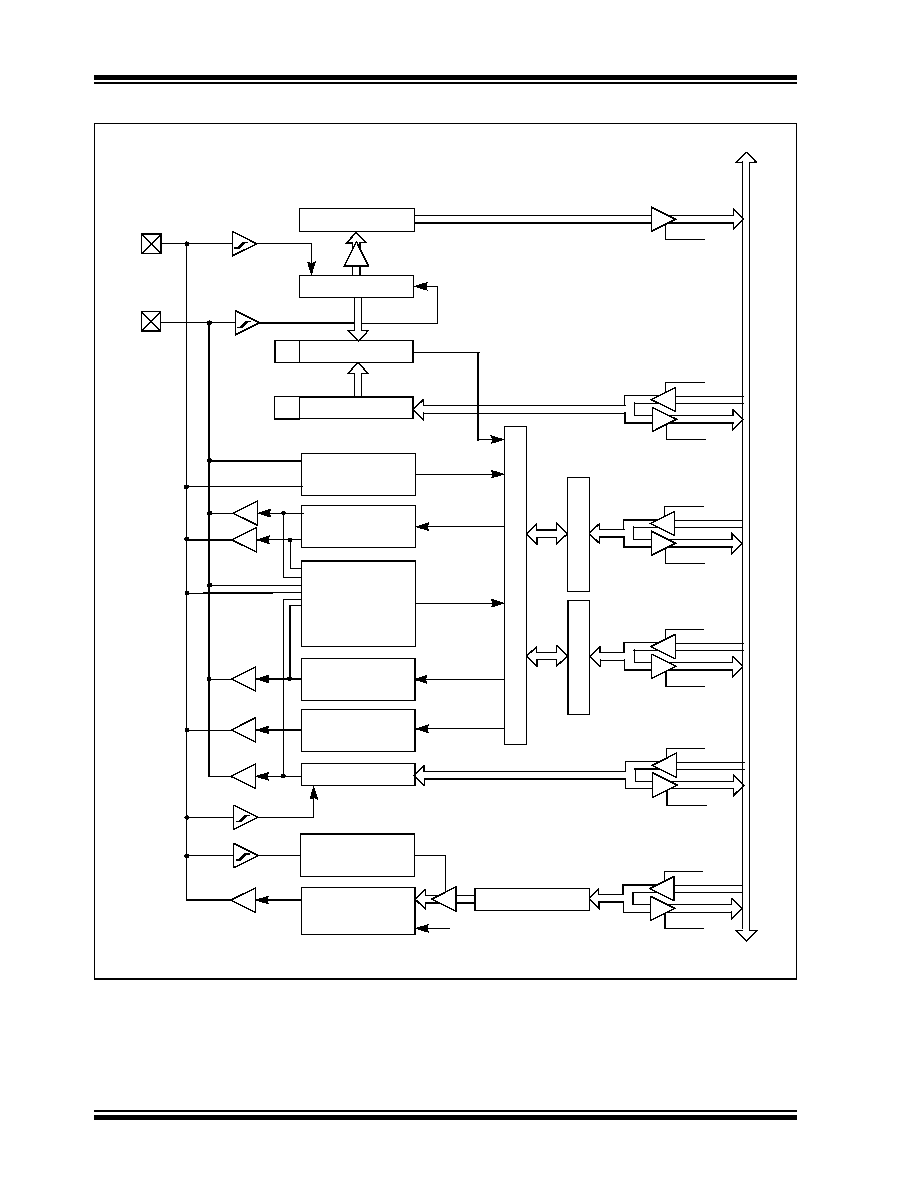
dsPIC30F1010/202X
DS70178A-page 150
Advance Information
©
2006 Microchip Technology Inc.
FIGURE 14-2:
I
2
CTM BLOCK DIAGRAM
I2CRSR
I2CRCV
Internal
Data Bus
SCL
SDA
Shift
Match Detect
I2CADD
Start and
Stop bit Detect
Clock
Addr_Match
Clock
Stretching
I2CTRN
LSB
Shift
Clock
Write
Read
BRG Down
I2CBRG
Reload
Control
F
CY
Start, Restart,
Stop bit Generate
Write
Read
Acknowledge
Generation
Collision
Detect
Write
Read
Write
Read
I2CCON
Write
Read
I2
C
S
T
A
T
Cont
r
o
l Logic
Read
LSB
Counter

©
2006 Microchip Technology Inc.
Advance Information
DS70178A-page 151
dsPIC30F1010/202X
14.2
I
2
C Module Addresses
The I2CADD register contains the Slave mode
addresses. The register is a 10-bit register.
If the A10M bit (I2CCON<10>) is `
0
', the address is
interpreted by the module as a 7-bit address. When an
address is received, it is compared to the 7 Least
Significant bits of the I2CADD register.
If the A10M bit is `
1
', the address is assumed to be a
10-bit address. When an address is received, it will be
compared with the binary value `
1
1
1
1
0
A9
A8
'
(where
A9,
A8
are two Most Significant bits of
I2CADD). If that value matches, the next address will
be compared with the Least Significant 8 bits of
I2CADD, as specified in the 10-bit addressing protocol.
14.3
I
2
C 7-bit Slave Mode Operation
Once enabled (I2CEN =
1
), the slave module will wait
for a Start bit to occur (i.e., the I
2
C module is `Idle'). Fol-
lowing the detection of a Start bit, 8 bits are shifted into
I2CRSR and the address is compared against
I2CADD. In 7-bit mode (A10M =
0
), bits I2CADD<6:0>
are compared against I2CRSR<7:1> and I2CRSR<0>
is the R_W bit. All incoming bits are sampled on the
rising edge of SCL.
If an address match occurs, an acknowledgement will
be sent, and the slave event interrupt flag (SI2CIF) is
set on the falling edge of the ninth (ACK) bit. The
address match does not affect the contents of the
I2CRCV buffer or the RBF bit.
14.3.1
SLAVE TRANSMISSION
If the R_W bit received is a `
1
', then the serial port will
go into Transmit mode. It will send ACK on the ninth bit
and then hold SCL to `
0
' until the CPU responds by writ-
ing to I2CTRN. SCL is released by setting the SCLREL
bit, and 8 bits of data are shifted out. Data bits are
shifted out on the falling edge of SCL, such that SDA is
valid during SCL high (see timing diagram). The inter-
rupt pulse is sent on the falling edge of the ninth clock
pulse, regardless of the status of the ACK received
from the master.
14.3.2
SLAVE RECEPTION
If the R_W bit received is a `
0
' during an address
match, then Receive mode is initiated. Incoming bits
are sampled on the rising edge of SCL. After 8 bits are
received, if I2CRCV is not full or I2COV is not set,
I2CRSR is transferred to I2CRCV. ACK is sent on the
ninth clock.
If the RBF flag is set, indicating that I2CRCV is still
holding data from a previous operation (RBF =
1
), then
ACK is not sent; however, the interrupt pulse is gener-
ated. In the case of an overflow, the contents of the
I2CRSR are not loaded into the I2CRCV.
14.4
I
2
C 10-bit Slave Mode Operation
In 10-bit mode, the basic receive and transmit opera-
tions are the same as in the 7-bit mode. However, the
criteria for address match is more complex.
The I
2
C specification dictates that a slave must be
addressed for a write operation, with two address bytes
following a Start bit.
The A10M bit is a control bit that signifies that the
address in I2CADD is a 10-bit address rather than a
7-bit address. The address detection protocol for the
first byte of a message address is identical for 7-bit
and 10-bit messages, but the bits being compared are
different.
I2CADD holds the entire 10-bit address. Upon receiv-
ing an address following a Start bit, I2CRSR <7:3> is
compared against a literal `
11110
' (the default 10-bit
address) and I2CRSR<2:1> are compared against
I2CADD<9:8>. If a match occurs and if R_W =
0
, the
interrupt pulse is sent. The ADD10 bit will be cleared to
indicate a partial address match. If a match fails or
R_W =
1
, the ADD10 bit is cleared and the module
returns to the Idle state.
The low byte of the address is then received and com-
pared with I2CADD<7:0>. If an address match occurs,
the interrupt pulse is generated and the ADD10 bit is
set, indicating a complete 10-bit address match. If an
address match did not occur, the ADD10 bit is cleared
and the module returns to the Idle state.
14.4.1
10-BIT MODE SLAVE
TRANSMISSION
Once a slave is addressed in this fashion, with the full
10-bit address (we will refer to this state as
"PRIOR_ADDR_MATCH"), the master can begin send-
ing data bytes for a slave reception operation.
14.4.2
10-BIT MODE
SLAVE RECEPTION
Once addressed, the master can generate a Repeated
Start, reset the high byte of the address and set the
R_W bit without generating a Stop bit, thus initiating a
slave transmit operation.
Note:
The I2CRCV will be loaded if the I2COV
bit =
1
and the RBF flag =
0
. In this case,
a read of the I2CRCV was performed, but
the user did not clear the state of the
I2COV bit before the next receive
occurred. The acknowledgement is not
sent (ACK =
1
) and the I2CRCV is
updated.

dsPIC30F1010/202X
DS70178A-page 152
Advance Information
©
2006 Microchip Technology Inc.
14.5
Automatic Clock Stretch
In the Slave modes, the module can synchronize buffer
reads and write to the master device by clock
stretching.
14.5.1
TRANSMIT CLOCK STRETCHING
Both 10-bit and 7-bit Transmit modes implement clock
stretching by asserting the SCLREL bit after the falling
edge of the ninth clock if the TBF bit is cleared,
indicating the buffer is empty.
In Slave Transmit modes, clock stretching is always
performed, irrespective of the STREN bit.
Clock synchronization takes place following the ninth
clock of the transmit sequence. If the device samples
an ACK on the falling edge of the ninth clock, and if the
TBF bit is still clear, then the SCLREL bit is automati-
cally cleared. The SCLREL being cleared to `
0
' will
assert the SCL line low. The user's ISR must set the
SCLREL bit before transmission is allowed to con-
tinue. By holding the SCL line low, the user has time to
service the ISR and load the contents of the I2CTRN
before the master device can initiate another transmit
sequence.
14.5.2
RECEIVE CLOCK STRETCHING
The STREN bit in the I2CCON register can be used to
enable clock stretching in Slave Receive mode. When
the STREN bit is set, the SCL pin will be held low at
the end of each data receive sequence.
14.5.3
CLOCK STRETCHING DURING
7-BIT ADDRESSING (STREN =
1
)
When the STREN bit is set in Slave Receive mode,
the SCL line is held low when the buffer register is full.
The method for stretching the SCL output is the same
for both 7 and 10-bit Addressing modes.
Clock stretching takes place following the ninth clock of
the receive sequence. On the falling edge of the ninth
clock at the end of the ACK sequence, if the RBF bit is
set, the SCLREL bit is automatically cleared, forcing the
SCL output to be held low. The user's ISR must set the
SCLREL bit before reception is allowed to continue. By
holding the SCL line low, the user has time to service
the ISR and read the contents of the I2CRCV before the
master device can initiate another receive sequence.
This will prevent buffer overruns from occurring.
14.5.4
CLOCK STRETCHING DURING
10-BIT ADDRESSING (STREN =
1
)
Clock stretching takes place automatically during the
addressing sequence. Because this module has a
register for the entire address, it is not necessary for
the protocol to wait for the address to be updated.
After the address phase is complete, clock stretching
will occur on each data receive or transmit sequence
as was described earlier.
14.6
Software Controlled Clock
Stretching (STREN =
1
)
When the STREN bit is `
1
', the SCLREL bit may be
cleared by software to allow software to control the
clock stretching. The logic will synchronize writes to
the SCLREL bit with the SCL clock. Clearing the
SCLREL bit will not assert the SCL output until the
module detects a falling edge on the SCL output and
SCL is sampled low. If the SCLREL bit is cleared by
the user while the SCL line has been sampled low, the
SCL output will be asserted (held low). The SCL out-
put will remain low until the SCLREL bit is set, and all
other devices on the I
2
C bus have deasserted SCL.
This ensures that a write to the SCLREL bit will not
violate the minimum high time requirement for SCL.
If the STREN bit is `
0
', a software write to the SCLREL
bit will be disregarded and have no effect on the
SCLREL bit.
14.7
Interrupts
The I
2
C module generates two interrupt flags, MI2CIF
(I
2
C Master Interrupt Flag) and SI2CIF (I
2
C Slave Inter-
rupt Flag). The MI2CIF interrupt flag is activated on
completion of a master message event. The SI2CIF
interrupt flag is activated on detection of a message
directed to the slave.
Note 1: If the user loads the contents of I2CTRN,
setting the TBF bit before the falling edge
of the ninth clock, the SCLREL bit will not
be cleared and clock stretching will not
occur.
2: The SCLREL bit can be set in software,
regardless of the state of the TBF bit.
Note 1: If the user reads the contents of the
I2CRCV, clearing the RBF bit before the
falling edge of the ninth clock, the
SCLREL bit will not be cleared and clock
stretching will not occur.
2: The SCLREL bit can be set in software,
regardless of the state of the RBF bit. The
user should be careful to clear the RBF bit
in the ISR before the next receive
sequence in order to prevent an Overflow
condition.

©
2006 Microchip Technology Inc.
Advance Information
DS70178A-page 153
dsPIC30F1010/202X
14.8
Slope Control
The I
2
C standard requires slope control on the SDA
and SCL signals for Fast mode (400 kHz). The control
bit, DISSLW, enables the user to disable slew rate con-
trol, if desired. It is necessary to disable the slew rate
control for 1 MHz mode.
14.9
IPMI Support
The control bit IPMIEN enables the module to support
Intelligent Peripheral Management Interface (IPMI).
When this bit is set, the module accepts and acts upon
all addresses.
14.10 General Call Address Support
The general call address can address all devices.
When this address is used, all devices should,
in theory, respond with an acknowledgement.
The general call address is one of eight addresses
reserved for specific purposes by the I
2
C protocol. It
consists of all `
0
's with R_W =
0
.
The general call address is recognized when the Gen-
eral Call Enable (GCEN) bit is set (I2CCON<15> =
1
).
Following a Start bit detection, 8 bits are shifted into
I2CRSR and the address is compared with I2CADD,
and is also compared with the general call address
which is fixed in hardware.
If a general call address match occurs, the I2CRSR is
transferred to the I2CRCV after the eighth clock, the
RBF flag is set, and, on the falling edge of the ninth bit
(ACK bit), the master event interrupt flag (MI2CIF) is
set.
When the interrupt is serviced, the source for the inter-
rupt can be checked by reading the contents of the
I2CRCV to determine if the address was device
specific, or a general call address.
14.11 I
2
C Master Support
As a Master device, six operations are supported.
∑ Assert a Start condition on SDA and SCL.
∑ Assert a Restart condition on SDA and SCL.
∑ Write to the I2CTRN register initiating
transmission of data/address.
∑ Generate a Stop condition on SDA and SCL.
∑ Configure the I
2
C port to receive data.
∑ Generate an ACK condition at the end of a
received byte of data.
14.12 I
2
C Master Operation
The master device generates all of the serial clock
pulses and the Start and Stop conditions. A transfer is
ended with a Stop condition or with a Repeated Start
condition. Since the Repeated Start condition is also
the beginning of the next serial transfer, the I
2
C bus will
not be released.
In Master Transmitter mode, serial data is output
through SDA, while SCL outputs the serial clock. The
first byte transmitted contains the slave address of the
receiving device (7 bits) and the data direction bit. In
this case, the data direction bit (R_W) is logic `
0
'. Serial
data is transmitted 8 bits at a time. After each byte is
transmitted, an ACK bit is received. Start and Stop con-
ditions are output to indicate the beginning and the end
of a serial transfer.
In Master Receive mode, the first byte transmitted con-
tains the slave address of the transmitting device (7
bits) and the data direction bit. In this case, the data
direction bit (R_W) is logic
1
. Thus, the first byte trans-
mitted is a 7-bit slave address, followed by a `
1
' to indi-
cate receive bit. Serial data is received via SDA, while
SCL outputs the serial clock. Serial data is received 8
bits at a time. After each byte is received, an ACK bit is
transmitted. Start and Stop conditions indicate the
beginning and end of transmission.
14.12.1
I
2
C MASTER TRANSMISSION
Transmission of a data byte, a 7-bit address, or the sec-
ond half of a 10-bit address is accomplished by simply
writing a value to I2CTRN register. The user should
only write to I2CTRN when the module is in a WAIT
state. This action will set the Buffer Full Flag (TBF) and
allow the Baud Rate Generator to begin counting and
start the next transmission. Each bit of address/data
will be shifted out onto the SDA pin after the falling
edge of SCL is asserted. The Transmit Status Flag,
TRSTAT (I2CSTAT<14>), indicates that a master
transmit is in progress.
14.12.2
I
2
C MASTER RECEPTION
Master mode reception is enabled by programming the
receive enable (RCEN) bit (I2CCON<11>). The I
2
C
module must be Idle before the RCEN bit is set, other-
wise the RCEN bit will be disregarded. The Baud Rate
Generator begins counting, and, on each rollover, the
state of the SCL pin toggles, and data is shifted in to the
I2CRSR on the rising edge of each clock.

dsPIC30F1010/202X
DS70178A-page 154
Advance Information
©
2006 Microchip Technology Inc.
14.12.3
BAUD RATE GENERATOR
In I
2
C Master mode, the reload value for the BRG is
located in the I2CBRG register. When the BRG is
loaded with this value, the BRG counts down to `
0
' and
stops until another reload has taken place. If clock
arbitration is taking place, for instance, the BRG is
reloaded when the SCL pin is sampled high.
As per the I
2
C standard, FSCK may be 100 kHz or
400 kHz. However, the user can specify any baud rate
up to 1 MHz. I2CBRG values of `
0
' or `
1
' are illegal.
EQUATION 14-1:
I2CBRG VALUE
14.12.4
CLOCK ARBITRATION
Clock arbitration occurs when the master deasserts the
SCL pin (SCL allowed to float high) during any receive,
transmit or Restart/Stop condition. When the SCL pin is
allowed to float high, the Baud Rate Generator is
suspended from counting until the SCL pin is actually
sampled high. When the SCL pin is sampled high, the
Baud Rate Generator is reloaded with the contents of
I2CBRG and begins counting. This ensures that the
SCL high time will always be at least one BRG rollover
count in the event that the clock is held low by an
external device.
14.12.5
MULTI-MASTER COMMUNICATION,
BUS COLLISION AND BUS
ARBITRATION
Multi-Master operation support is achieved by bus
arbitration. When the master outputs address/data bits
onto the SDA pin, arbitration takes place when the
master outputs a `
1
' on SDA, by letting SDA float high
while another master asserts a `
0
'. When the SCL pin
floats high, data should be stable. If the expected data
on SDA is a `
1
' and the data sampled on the SDA
pin =
0
, then a bus collision has taken place. The
master will set the MI2CIF pulse and reset the master
portion of the I
2
C port to its Idle state.
If a transmit was in progress when the bus collision
occurred, the transmission is halted, the TBF flag is
cleared, the SDA and SCL lines are deasserted, and a
value can now be written to I2CTRN. When the user
services the I
2
C master event Interrupt Service
Routine, if the I
2
C bus is free (i.e., the P bit is set) the
user can resume communication by asserting a Start
condition.
If a Start, Restart, Stop or Acknowledge condition was
in progress when the bus collision occurred, the condi-
tion is aborted, the SDA and SCL lines are deasserted,
and the respective control bits in the I2CCON register
are cleared to `
0
'. When the user services the bus col-
lision Interrupt Service Routine, and if the I
2
C bus is
free, the user can resume communication by asserting
a Start condition.
The Master will continue to monitor the SDA and SCL
pins and, if a Stop condition occurs, the MI2CIF bit will
be set.
A write to the I2CTRN will start the transmission of data
at the first data bit, regardless of where the transmitter
left off when bus collision occurred.
In a Multi-Master environment, the interrupt generation
on the detection of Start and Stop conditions allows the
determination of when the bus is free. Control of the I
2
C
bus can be taken when the P bit is set in the I2CSTAT
register, or the bus is Idle and the S and P bits are
cleared.
14.13 I
2
C Module Operation During CPU
Sleep and Idle Modes
14.13.1
I
2
C OPERATION DURING CPU
SLEEP MODE
When the device enters Sleep mode, all clock sources
to the module are shutdown and stay at logic `
0
'. If
Sleep occurs in the middle of a transmission, and the
state machine is partially into a transmission as the
clocks stop, then the transmission is aborted. Similarly,
if Sleep occurs in the middle of a reception, then the
reception is aborted.
14.13.2
I
2
C OPERATION DURING CPU IDLE
MODE
For the I
2
C, the I2CSIDL bit selects if the module will
stop on Idle or continue on Idle. If I2CSIDL =
0
, the
module will continue operation on assertion of the Idle
mode. If I2CSIDL =
1
, the module will stop on Idle.
I2CBRG
Fcy
Fscl
-----------
Fcy
1 111 111
,
,
---------------------------
≠
1
≠
=
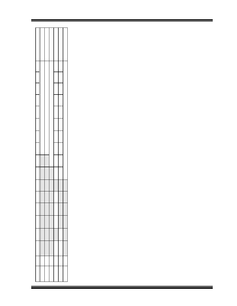
©
2006 Microchip Technology Inc.
Advance Information
DS70178A-page 155
dsPIC30F1010/202X
TA
B
L
E
1
4
-
1
:
I
2
CTM
RE
GIS
T
E
R
MAP
Note
:
Ref
e
r to
th
e "
ds
PIC
3
0F F
a
mi
ly
R
e
fe
ren
c
e
Ma
nua
l"
(D
S7
004
6) f
o
r de
sc
rip
t
io
ns
of re
gi
ste
r
bi
t fi
eld
s
.
S
F
R
Nam
e
Ad
d
r
.
B
it
15
Bit
14
Bit
13
Bit
12
Bit
1
1
Bit
10
B
i
t 9
B
it
8
B
it
7
B
it
6
B
i
t
5
B
it
4
B
it
3
B
it
2
B
it
1
B
i
t
0
R
e
s
e
t
S
t
at
e
I
2
CRCV
0
2
0
0
--
--
--
--
--
--
--
--
Re
ce
ive
Re
g
i
s
t
e
r
0000
0000 0000 0000
I
2
CT
RN
0
2
0
2
--
--
--
--
--
--
--
--
T
r
a
n
sm
it
Re
g
i
s
t
e
r
0000
0000 1111 1111
I
2
CBRG
0
2
0
4
--
--
--
--
--
--
--
B
a
u
d
Ra
te G
ene
ra
tor
0000
0000 0000 0000
I
2
C
C
O
N
020
6
I
2C
E
N
--
I2
CSIDL
S
CL
REL
I
P
M
IEN
--
DI
SSL
W
S
M
E
N
G
CEN
S
TREN
ACKDT
A
CKE
N
RCEN
PEN
R
S
EN
S
E
N
0001
0000 0000 0000
I
2
CST
A
T
0
2
0
8
A
CKST
A
T
TRST
A
T
--
--
--
--
GCS
T
A
T
A
DD1
0
I
W
C
OL
I2C
O
V
D
_A
P
S
R_
W
R
B
F
T
B
F
0000
0000 0000 0000
I
2
CADD
0
2
0
A
--
--
--
--
--
--
A
ddr
ess R
egi
st
er
0000
0000 0000 0000

dsPIC30F1010/202X
DS70178A-page 156
Advance Information
©
2006 Microchip Technology Inc.
NOTES:

©
2006 Microchip Technology Inc.
Advance Information
DS70178A-page 157
dsPIC30F1010/202X
15.0
UNIVERSAL ASYNCHRONOUS
RECEIVER TRANSMITTER
(UART) MODULE
The Universal Asynchronous Receiver Transmitter
(UART) module is one of the serial I/O modules
available in the dsPIC30F1010/202X device family.
The UART is a full-duplex asynchronous system that
can communicate with peripheral devices, such as
personal computers, LIN, RS-232 and RS-485 inter-
faces. The module also includes an IrDA encoder and
decoder
.
The primary features of the UART module are:
∑ Full-Duplex 8 or 9-bit Data Transmission through
the U1TX and U1RX pins
∑ Even, Odd or No Parity Options (for 8-bit data)
∑ One or Two Stop bits
∑ Fully Integrated Baud Rate Generator with 16-bit
Prescaler
∑ Baud Rates Ranging from 1 Mbps to 15 bps at
16 MIPS
∑ 4-Deep First-In-First-Out (FIFO) Transmit Data
Buffer
∑ 4-Deep FIFO Receive Data Buffer
∑ Parity, Framing and Buffer Overrun Error Detection
∑ Support for 9-bit mode with Address Detect
(9th bit =
1
)
∑ Transmit and Receive Interrupts
∑ Loopback mode for Diagnostic Support
∑ Support for Sync and Break Characters
∑ Supports Automatic Baud Rate Detection
∑ IrDA Encoder and Decoder Logic
∑ 16x Baud Clock Output for IrDA Support
A simplified block diagram of the UART is shown in
Figure 15-1. The UART module consists of these key
important hardware elements:
∑ Baud Rate Generator
∑ Asynchronous Transmitter
∑ Asynchronous Receiver
FIGURE 15-1:
UART SIMPLIFIED BLOCK DIAGRAM
Note: This data sheet summarizes features of this group
of dsPIC30F devices and is not intended to be a complete
reference source. For more information on the CPU,
peripherals, register descriptions and general device
functionality, refer to the "dsPIC30F Family Reference
Manual" (DS70046).
U1RX
IrDA
Æ
UART1 Receiver
UART1 Transmitter
U1TX
Baud Rate Generator

dsPIC30F1010/202X
DS70178A-page 158
Advance Information
©
2006 Microchip Technology Inc.
15.1
UART Baud Rate Generator (BRG)
The UART module includes a dedicated 16-bit Baud
Rate Generator. The U1BRG register controls the
period of a free-running 16-bit timer. Equation 15-1
shows the formula for computation of the baud rate
with BRGH =
0
.
EQUATION 15-1:
UART BAUD RATE WITH
BRGH =
0
(1,2)
Example 15-1 shows the calculation of the baud rate
error for the following conditions:
∑ F
CY
= 4 MHz
∑ Desired Baud Rate = 9600
The maximum baud rate (BRGH =
0
) possible is
F
CY
/16 (for U1BRG =
0
), and the minimum baud rate
possible is F
CY
/(16 * 65536).
Equation 15-2 shows the formula for computation of
the baud rate with BRGH =
1
.
EQUATION 15-2:
UART BAUD RATE WITH
BRGH =
1
(1,2)
The maximum baud rate (BRGH =
1
) possible is F
CY
/4
(for U1BRG =
0
) and the minimum baud rate possible
is F
CY
/(4 * 65536).
Writing a new value to the U1BRG register causes the
BRG timer to be reset (cleared). This ensures the BRG
does not wait for a timer overflow before generating the
new baud rate.
EXAMPLE 15-1:
BAUD RATE ERROR CALCULATION (BRGH =
0
)
(1)
Note 1: F
CY
denotes the instruction cycle clock
frequency (F
OSC
/2
).
2: Based on T
CY
= 2/F
OSC
, PLL are
disabled.
Baud Rate =
F
CY
16 ∑ (U1BRG + 1)
F
CY
16 ∑ Baud Rate
U1BRG =
≠ 1
Baud Rate =
F
CY
4 ∑ (U1BRG + 1)
F
CY
4 ∑ Baud Rate
U1BRG =
≠ 1
Note 1: F
CY
denotes the instruction cycle clock
frequency
.
2: Based on T
CY
= 2/F
OSC
, PLL are
disabled.
Desired Baud Rate
= F
CY
/(16 (U1BRG + 1))
Solving for U1BRG value:
U1BRG
=
((F
CY
/Desired Baud Rate)/16) ≠ 1
U1BRG
=
((4000000/9600)/16) ≠ 1
U1BRG
=
25
Calculated Baud Rate
=
4000000/(16 (25 + 1))
=
9615
Error
=
(Calculated Baud Rate ≠ Desired Baud Rate)
Desired Baud Rate
=
(9615 ≠ 9600)/9600
=
0.16%
Note 1: Based on T
CY
= 2/F
OSC
, PLL are disabled.

©
2006 Microchip Technology Inc.
Advance Information
DS70178A-page 159
dsPIC30F1010/202X
15.2
Transmitting in 8-bit Data Mode
1.
Set up the UART:
a)
Write appropriate values for data, parity and
Stop bits.
b)
Write appropriate baud rate value to the
U1BRG register.
c)
Set up transmit and receive interrupt enable
and priority bits.
2.
Enable the UART.
3.
Set the UTXEN bit (causes a transmit interrupt).
4.
Write data byte to lower byte of TXxREG word.
The value will be immediately transferred to the
Transmit Shift Register (TSR), and the serial bit
stream will start shifting out with next rising edge
of the baud clock.
5.
Alternately, the data byte may be transferred
while UTXEN =
0
, and then the user may set
UTXEN. This will cause the serial bit stream to
begin immediately because the baud clock will
start from a cleared state.
6.
A transmit interrupt will be generated as per
interrupt control bit, UTXISELx.
15.3
Transmitting in 9-bit Data Mode
1.
Set up the UART (as described in Section 15.2
"Transmitting in 8-bit Data Mode").
2.
Enable the UART.
3.
Set the UTXEN bit (causes a transmit interrupt).
4.
Write TXxREG as a 16-bit value only.
5.
A word write to TXxREG triggers the transfer of
the 9-bit data to the TSR. Serial bit stream will
start shifting out with the first rising edge of the
baud clock.
6.
A transmit interrupt will be generated as per the
setting of control bit, UTXISELx.
15.4
Break and Sync Transmit
Sequence
The following sequence will send a message frame
header made up of a Break, followed by an auto-baud
Sync byte.
1.
Configure the UART for the desired mode.
2.
Set UTXEN and UTXBRK ≠ sets up the Break
character,
3.
Load the TXxREG with a dummy character to
initiate transmission (value is ignored).
4.
Write `55h' to TXxREG ≠ loads Sync character
into the transmit FIFO.
5.
After the Break has been sent, the UTXBRK bit
is reset by hardware. The Sync character now
transmits.
15.5
Receiving in 8-bit or 9-bit Data
Mode
1.
Set up the UART (as described in Section 15.2
"Transmitting in 8-bit Data Mode").
2.
Enable the UART.
3.
A receive interrupt will be generated when one
or more data characters have been received as
per interrupt control bit, URXISELx.
4.
Read the OERR bit to determine if an overrun
error has occurred. The OERR bit must be reset
in software.
5.
Read RXxREG.
The act of reading the RXxREG character will move the
next character to the top of the receive FIFO, including
a new set of PERR and FERR values.
15.6
Built-in IrDA Encoder and Decoder
The UART has full implementation of the IrDA encoder
and decoder as part of the UART module. The built-in
IrDA encoder and decoder functionality is enabled
using the IREN bit U1MODE<12>. When enabled
(IREN =
1
), the receive pin (U1RX) acts as the input
from the infrared receiver. The transmit pin (U1TX) acts
as the output to the infrared transmitter.
15.7
Alternate UART I/O Pins
An alternate set of I/O pins, U1ATX and U1ARX can be
used for communications. The alternate UART pins are
useful when the primary UART pins are shared by other
peripherals. The alternate I/O pins are enabled by set-
ting the ALTIO bit in the UxMODE register. If ALTIO =
1
, the U1ATX and U1ARX pins are used by the UART
module, instead of the U1TX and U1RX pins. If ALTIO
=
0
, the U1TX and U1RX pins are used by the UART
module.

dsPIC30F1010/202X
DS70178A-page 160
Advance Information
©
2006 Microchip Technology Inc.
REGISTER 15-1:
U1MODE: UART1 MODE REGISTER
R/W-0
U-0
R/W-0
R/W-0
U-0
R/W-0
U-0
U-0
UARTEN
≠
USIDL
IREN
≠
ALTIO
≠
≠
bit 15
bit 8
R/W-0 HC
R/W-0
R/W-0 HC
R/W-0
R/W-0
R/W-0
R/W-0
R/W-0
WAKE
LPBACK
ABAUD
RXINV
BRGH
PDSEL1
PDSEL0
STSEL
bit 7
bit 0
Legend:
U = Unimplemented bit, read as `0'
R = Readable bit
W = Writable bit
HC = Hardware Cleared
HS = Hardware Select
-n = Value at POR
`1' = Bit is set
`0' = Bit is cleared
x = Bit is unknown
bit 15
UARTEN: UART1 Enable bit
1
= UART1 is enabled; all UART1 pins are controlled by UART1 as defined by UEN<1:0>
0
= UART1 is disabled; all UART1 pins are controlled by PORT latches; UART1 power consumption
minimal
bit 14
Unimplemented: Read as `
0
'
bit 13
USIDL: Stop in Idle Mode bit
1
= Discontinue module operation when device enters Idle mode
0
= Continue module operation in Idle mode
bit 12
IREN: IrDA Encoder and Decoder Enable bit
1
= IrDA encoder and decoder enabled
0
= IrDA encoder and decoder disabled
Note:
This feature is only available for the 16x BRG mode (BRGH =
0
).
bit 11
Unimplemented: Read as `
0
'
bit 10
ALTIO: UART Alternate I/O Selection bit
1
= UART communicates using U1ATX and U1ARX I/O pins
0
= UART communicates using U1TX and U1RX I/O pins.
bit 9-8
Unimplemented: Read as `
0
'
bit 7
WAKE: Wake-up on Start bit Detect During Sleep Mode Enable bit
1
= UART1 will continue to sample the U1RX pin; interrupt generated on falling edge, bit cleared in
hardware on following rising edge
0
= No wake-up enabled
bit 6
LPBACK: UART1 Loopback Mode Select bit
1
= Enable Loopback mode
0
= Loopback mode is disabled
bit 5
ABAUD: Auto-Baud Enable bit
1
= Enable baud rate measurement on the next character ≠ requires reception of a Sync field (55h);
cleared in hardware upon completion
0
= Baud rate measurement disabled or completed
bit 4
RXINV: Receive Polarity Inversion bit
1
=
U1RX Idle state is `
0
'
0
= U1RX Idle state is `
1
'
bit 3
BRGH: High Baud Rate Enable bit
1
= BRG generates 4 clocks per bit period (4x Baud Clock, High-Speed mode)
0
= BRG generates 16 clocks per bit period (16x Baud Clock, Standard mode)

©
2006 Microchip Technology Inc.
Advance Information
DS70178A-page 161
dsPIC30F1010/202X
bit 2-1
PDSEL1:PDSEL0: Parity and Data Selection bits
11
= 9-bit data, no parity
10
= 8-bit data, odd parity
01
= 8-bit data, even parity
00
= 8-bit data, no parity
bit 0
STSEL: Stop Bit Selection bit
1
= Two Stop bits
0
= One Stop bit
REGISTER 15-1:
U1MODE: UART1 MODE REGISTER

dsPIC30F1010/202X
DS70178A-page 162
Advance Information
©
2006 Microchip Technology Inc.
REGISTER 15-2:
U1STA: UART1 STATUS AND CONTROL REGISTER
R/W-0
R/W-0
R/W-0
U-0
R/W-0
R/W-0
R/W-0
R/W-0
UTXISEL1
UTXINV
(1)
UTXISEL0
--
UTXBRK
UTXEN
UTXBF
TRMT
bit 15
bit 8
R/W-0
R/W-0
R/W-0
R/W-0
R/W-0
R/W-0
R/W-0
R/W-0
URXISEL1
URXISEL0
ADDEN
RIDLE
PERR
FERR
OERR
URXDA
bit 7
bit 0
Legend:
U = Unimplemented bit, read as `0'
R = Readable bit
W = Writable bit
HS =Hardware Set
HC = Hardware Cleared
-n = Value at POR
`1' = Bit is set
`0' = Bit is cleared
x = Bit is unknown
bit 15, 13
UTXISEL1:UTXISEL0: Transmission Interrupt Mode Selection bits
11
= Reserved; do not use
10
= Interrupt when a character is transferred to the Transmit Shift Register and as a result, the
transmit buffer becomes empty
01
= Interrupt when the last character is shifted out of the Transmit Shift Register; all transmit
operations are completed
00
=Interrupt when a character is transferred to the Transmit Shift Register (this implies there is at
least one character open in the transmit buffer)
bit 14
UTXINV: IrDA Encoder Transmit Polarity Inversion bit
(1)
1
= IrDA encoded U1TX idle state is `
1
'
0
= IrDA encoded U1TX idle state is `
0
'
Note 1: Value of bit only affects the transmit properties of the module when the IrDA encoder is
enabled (IREN =
1
).
bit 12
Unimplemented: Read as `
0
'
bit 11
UTXBRK: Transmit Break bit
1
= Send Sync Break on next transmission ≠ Start bit, followed by twelve `
0
' bits, followed by Stop bit;
cleared by hardware upon completion
0
= Sync Break transmission disabled or completed
bit 10
UTXEN: Transmit Enable bit
1
= Transmit enabled, U1TX pin controlled by UART1
0
= Transmit disabled, any pending transmission is aborted and buffer is reset. U1TX pin controlled by
PORT.
bit 9
UTXBF: Transmit Buffer Full Status bit (Read-Only)
1
= Transmit buffer is full
0
= Transmit buffer is not full, at least one more character can be written
bit 8
TRMT: Transmit Shift Register Empty bit (Read-Only)
1
= Transmit Shift Register is empty and transmit buffer is empty (the last transmission has
completed)
0
= Transmit Shift Register is not empty, a transmission is in progress or queued
bit 7-6
URXISEL1:URXISEL0: Receive Interrupt Mode Selection bits
11
= Interrupt is set on RSR transfer, making the receive buffer full (i.e., has 4 data characters)
10
= Interrupt is set on RSR transfer, making the receive buffer 3/4 full (i.e., has 3 data characters)
0x
=Interrupt is set when any character is received and transferred from the RSR to the receive buffer.
Receive buffer has one or more characters.
bit 5
ADDEN: Address Character Detect bit (bit 8 of received data =
1
)
1
= Address Detect mode enabled. If 9-bit mode is not selected, this does not take effect.
0 = Address Detect mode disabled

©
2006 Microchip Technology Inc.
Advance Information
DS70178A-page 163
dsPIC30F1010/202X
bit 4
RIDLE: Receiver Idle bit (Read-Only)
1
= Receiver is Idle
0
= Receiver is active
bit 3
PERR: Parity Error Status bit (Read-Only)
1
= Parity error has been detected for the current character (character at the top of the receive FIFO)
0
= Parity error has not been detected
bit 2
FERR: Framing Error Status bit (Read-Only)
1
= Framing error has been detected for the current character (character at the top of the receive
FIFO)
0
= Framing error has not been detected
bit 1
OERR: Receive Buffer Overrun Error Status bit (Read/Clear-Only)
1
= Receive buffer has overflowed
0
= Receive buffer has not overflowed (clearing a previously set OERR bit (
1
0
transition) will reset
the receiver buffer and the RSR to the empty state)
bit 0
URXDA: Receive Buffer Data Available bit (Read-Only)
1
= Receive buffer has data, at least one more character can be read
0
= Receive buffer is empty
REGISTER 15-2:
U1STA: UART1 STATUS AND CONTROL REGISTER

dsPIC30F1010/202X
DS70178A-page 164
Advance Information
©
2006 Microchip Technology Inc.
T
A
BLE
1
5
-1:
UART1
RE
GIS
T
E
R
M
A
P
SF
R Na
m
e
SF
R
Ad
d
r
Bi
t 1
5
Bi
t 1
4
Bit
13
Bi
t 1
2
Bi
t 1
1
Bit
10
Bit 9
B
it 8
B
it 7
B
i
t
6
B
it
5
B
i
t
4
B
it
3
B
it
2
B
it
1
B
it
0
All
R
ese
t
s
U1
M
O
DE
02
20
UA
R
T
EN
--U
S
I
D
L
I
R
E
N
--A
L
T
I
O
--
--
W
A
K
E
L
PBAC
K
A
B
A
UD
R
X
I
N
V
B
RG
H
P
D
SEL
<1
:
0
>
S
T
SEL
0000
U1
ST
A
0
2
2
2
U
T
X
I
SEL
1
U
T
X
I
N
V
U
TXISEL
0
--
U
T
X
BRK
U
T
XEN
UT
XB
F
T
RM
T
URXISEL<1
:
0
>
A
DDEN
R
IDL
E
P
E
RR
F
E
RR
O
E
RR
URXDA
0110
U1
T
X
REG
0
2
2
4
--
--
--
--
--
--
--
U
A
R
T
T
r
an
s
m
i
t
R
e
gi
s
t
er
xxxx
U1
RXREG
0
2
2
6
--
--
--
--
--
--
--
U
A
R
T R
e
c
e
i
v
e
R
e
gi
s
t
er
0000
U1BRG
0
2
2
8
B
a
u
d
R
a
te
G
e
n
e
ra
to
r P
r
e
s
ca
le
r
0000
Le
ge
nd:
x
=
un
know
n
va
l
u
e o
n
R
e
set
,
-- =
uni
m
p
l
e
m
e
n
t
ed
, re
ad
as `
0
'.
Re
se
t va
lu
e
s
a
r
e
sh
o
w
n
in
h
e
xa
d
e
cim
a
l.

©
2006 Microchip Technology Inc.
Advance Information
DS70178A-page 165
dsPIC30F1010/202X
16.0
10-BIT 2 MSPS ANALOG-TO-
DIGITAL CONVERTER (ADC)
MODULE
The dsPIC30F1010/202X devices provide high-speed
successive approximation analog to digital conver-
sions to support applications such as AC/DC and
DC/DC power converters.
16.1
Features
∑ 10-bit resolution
∑ Uni-polar Inputs
∑ Up to 12 input channels
∑ ±1 LSB accuracy
∑ Single supply operation
∑ 2000 ksps conversion rate at 5V
∑ 1000 ksps conversion rate at 3.0V
∑ Low power CMOS technology
16.2
Description
This ADC module is designed for applications that
require low latency between the request for conversion
and the resultant output data. Typical applications
include:
∑ AC/DC power supplies
∑ DC/DC converters
∑ Power factor Correction
This ADC works with the Power Supply PWM module
in power control applications that require high-fre-
quency control loops. This module can sample and
convert two analog inputs in one microsecond. The one
microsecond conversion delay reduces the "phase lag"
between measurement and control system response.
Up to 4 inputs may be sampled at a time, and up to 12
inputs may request conversion at a time. If multiple
inputs request conversion, the ADC will convert them in
a sequential manner starting with the lowest order
input.
This ADC design provides each pair of analog inputs
(AN1,AN0), (AN3,AN2), ... , the ability to specify its own
trigger source out of a maximum of sixteen different
trigger sources. This capability allows this ADC to sam-
ple and convert analog inputs that are associated with
PWM generators operating on independent time
bases.
There is no operation during Sleep mode. The user
applications typically require synchronization between
analog data sampling and PWM output to the applica-
tion circuit. The very high speed operation of this ADC
module allows "data on demand".
In addition, several hardware features have been
added to the peripheral interface to improve real-time
performance in a typical DSP based application.
1.
Result alignment options
2.
Automated sampling
3.
External conversion start control
A block diagram of the ADC module is shown in
Figure 16-1.
16.3
Module Functionality
The 10-bit 2 Msps ADC is designed to support power
conversion applications when used with the Power
Supply PWM module. The 10-bit 2 Msps ADC samples
up to N (N
12) inputs at a time and then converts two
sampled inputs at a time. The quantity of sample and
hold circuits is determined by a device's requirements.
The10-Bit 2 Msps ADC produces two 10-bit conversion
results in 1 microsecond.
The ADC module supports up to 12 analog inputs. The
sampled inputs are connected, via multiplexers, to the
converter.
The analog reference voltage is defined as the device
supply voltage (AV
DD
/ AV
SS
).
The A/D module uses these Control and Status regis-
ters:
∑ A/D Control Register (ADCON)
∑ A/D Status Register (ADSTAT)
∑ A/D Base Register (ADBASE)(1)
∑ A/D Port Configuration Register (ADPCFG)
∑ A/D Convert Pair Control Register #0 (ADCPC0)
∑ A/D Convert Pair Control Register #1 (ADCPC1)
∑ A/D Convert Pair Control Register #2 (ADCPC2)
The ADCON register controls the operation of the ADC
module. The ADSTAT register displays the status of the
conversion processes. The ADPCFG registers config-
ure the port pins as analog inputs or as digital I/O. The
CPC registers control the triggering of the ADC conver-
sions. (See Register 16-1 through Register 16-7 for
detailed bit configurations.)
Note: A unique feature of the ADC module is its abil-
ity to sample inputs in an asynchronous manner. Indi-
vidual sample and hold circuits can be triggered
independently of each other.
Note: The PLL must be enabled for the ADC module
to function. This is achieved by using the
FNOSC<1:0> bits in the FOSCSEL Configuration
register.

dsPIC30F1010/202X
DS70178A-page 166
Advance Information
©
2006 Microchip Technology Inc.
FIGURE 16-1:
ADC BLOCK DIAGRAM
AV
SS
AV
DD
Da
t
a
B
u
s In
ter
f
ace
MUX / Sample / Sequence
Control
Fo
rm
at
DAC
12-word, 16-bit
Registers
Comparator
10-Bit SAR
Conversion Logic
AN0
AN2
AN6
AN1
AN11
AN3
AN8
AN10
Even numbered inputs
without dedicated S&H
Dedicated S&Hs
AN4

©
2006 Microchip Technology Inc.
Advance Information
DS70178A-page 167
dsPIC30F1010/202X
REGISTER 16-1:
A/D CONTROL REGISTER (ADCON)
R/W-0
U-0
R/W-0
U-0
U-0
R/W-0
U-0
R/W-0
ADON
--
ADSIDL
--
--
GSWTRG
--
FORM
bit 15
bit 8
R/W-0
R/W-0
R/W-0
U-0
U-0
R/W-0
R/W-1
R/W-1
EIE
ORDER
SEQSAMP
--
--
ADCS<2:0>
bit 7
bit 0
Legend:
R = Readable bit
W = Writable bit
U = Unimplemented bit, read as `0'
-n = Value at POR
`1' = Bit is set
`0' = Bit is cleared
x = Bit is unknown
bit 15
ADON: A/D Operating Mode bit
1
= A/D converter module is operating
0
= A/D converter is off
bit 14
Unimplemented: Read as `
0
'
bit 13
ADSIDL: Stop in Idle Mode bit
1
= Discontinue module operation when device enters Idle mode
0
= Continue module operation in Idle mode
bit 12-11
Unimplemented: Read as `
0
'
bit 10
GSWTRG: Global Software Trigger bit
When this bit is set by the user, it will trigger conversions if selected by the TRGSRC<4:0> bits in the
CPCx registers. This bit must be cleared by the user prior to initiating another global trigger (i.e., this
bit is not auto-clearing).
bit 9
Unimplemented: Read as `
0
'
bit 8
FORM: Data Output Format bit
1
= Fractional (D
OUT
=
dddd dddd dd00 0000
)
0
= Integer (D
OUT
=
0000 00dd dddd dddd
)
bit 7
EIE: Early Interrupt Enable bit
1
= Interrupt is generated after first conversion is completed
0
= Interrupt is generated after second conversion is completed
Note:
This control bit can only be changed while ADC is disabled (ADON =
0
).
bit 6
ORDER: Conversion Order bit
1
= Odd numbered analog input is converted first, followed by conversion of even numbered input
0
= Even numbered analog input is converted first, followed by conversion of odd numbered input
Note:
This control bit can only be changed while ADC is disabled (ADON =
0
).
bit 5
SEQSAMP: Sequential Sample Enable.
1
= Shared S&H is sampled at the start of the second conversion if ORDER =
0
. If ORDER =
1
, then
the shared S&H is sampled at the start of the first conversion.
0
= Shared S&H is sampled at the same time the dedicated S&H is sampled if the shared S&H is not
currently busy with an existing conversion process. If the shared S&H is busy at the time the
dedicated S&H is sampled, then the shared S&H will sample at the start of the new conversion
cycle
bit 4-3
Unimplemented: Read as `
0
'
bit 2-0
ADCS<2:0>: A/D Conversion Clock Select bits
111
= T
Q
∑
(ADCS<2:0> +1) = 8
∑
T
Q
∑∑∑∑∑
001
= T
Q
∑
(ADCS<2:0> +1) = 2
∑
T
Q
000
= T
Q
∑
(ADCS<2:0> +1) = 1
∑
T
Q
Note:
T
Q
= Period of System Clock @ 30 MIPS = 16.6 nsec (60 MHz)

dsPIC30F1010/202X
DS70178A-page 168
Advance Information
©
2006 Microchip Technology Inc.
REGISTER 16-2:
A/D STATUS REGISTER (ADSTAT)
U-0
U-0
U-0
U-0
U-0
U-0
U-0
U-0
--
--
--
--
--
--
--
--
bit 15
bit 8
U-0
U-0
R/C-0
H-S
R/C-0
H-S
R/C-0
H-S
R/C-0
H-S
R/C-0
H-S
R/C-0
H-S
--
--
P5RDY
P4RDY
P3RDY
P2RDY
P1RDY
P0RDY
bit 7
bit 0
Legend:
R = Readable bit
W = Writable bit
U = Unimplemented bit, read as `0'
-n = Value at POR
C = Clear in software
`1' = Bit is set
H-S = Set by hardware
`0' = Bit is cleared
x = Bit is unknown
bit 15-6
Unimplemented: Read as `
0
'
bit 5
P5RDY: Conversion Data for Pair #5 Ready bit
Bit set when data is ready in buffer, cleared when a `
0
' is written to this bit.
bit 4
P4RDY: Conversion Data for Pair #4 Ready bit
Bit set when data is ready in buffer, cleared when a `
0
' is written to this bit.
bit 3
P3RDY: Conversion Data for Pair #3 Ready bit
Bit set when data is ready in buffer, cleared when a `
0
' is written to this bit.
bit 2
P2RDY: Conversion Data for Pair #2 Ready bit
Bit set when data is ready in buffer, cleared when a `
0
' is written to this bit.
bit 1
P1RDY: Conversion Data for Pair #1 Ready bit
Bit set when data is ready in buffer, cleared when a `
0
' is written to this bit.
bit 0
P0RDY: Conversion Data for Pair #0 Ready bit
Bit set when data is ready in buffer, cleared when a `
0
' is written to this bit.

©
2006 Microchip Technology Inc.
Advance Information
DS70178A-page 169
dsPIC30F1010/202X
REGISTER 16-3:
A/D BASE REGISTER (ADBASE)
(1)
R/W-0
R/W-0
R/W-0
R/W-0
R/W-0
R/W-0
R/W-0
R/W-0
ADBASE<15:8>
bit 15
bit 8
R/W-0
R/W-0
R/W-0
R/W-0
R/W-0
R/W-0
R/W-0
U-0
ADBASE<7:1>
--
bit 7
bit 0
Legend:
R = Readable bit
W = Writable bit
U = Unimplemented bit, read as `0'
-n = Value at POR
`1' = Bit is set
`0' = Bit is cleared
x = Bit is unknown
bit 15-1
ADC Base Register: This register contains the base address of the user's ADC Interrupt Service Rou-
tine jump table. This register, when read, contains the sum of the ADBASE register contents and the
encoded value of the PxRDY Status bits.
The encoder logic provides the bit number of the highest priority PxRDY bits where P0RDY is the
highest priority, and P5RDY is lowest priority.
Note:
The encoding results are shifted left two bits so bits 1-0 of the result are always zero.
bit 0
Unimplemented: Read as `
0
'
Note 1: As an alternative to using the ADBASE register, the ADCP0-5 ADC pair conversion complete interrupts
(Interrupts 37-42) can be used to invoke A to D conversion completion routines for individual ADC input
pairs. Refer to Section 16.9 "Individual Pair Interrupts".
REGISTER 16-4:
A/D PORT CONFIGURATION REGISTER (ADPCFG)
U-0
U-0
U-0
U-0
R/W-0
R/W-0
R/W-0
R/W-0
--
--
--
--
PCFG11
PCFG10
PCFG9
PCFG8
bit 15
bit 8
R/W-0
R/W-0
R/W-0
R/W-0
R/W-0
R/W-0
R/W-0
R/W-0
PCFG7
PCFG6
PCFG5
PCFG4
PCFG3
PCFG2
PCFG1
PCFG0
bit 7
bit 0
Legend:
R = Readable bit
W = Writable bit
U = Unimplemented bit, read as `0'
-n = Value at POR
`1' = Bit is set
`0' = Bit is cleared
x = Bit is unknown
bit 15-12
Unimplemented: Read as `
0
'
bit 11-0
PCFG<11:0>: A/D Port Configuration Control bits
1
= Port pin in Digital mode, port read input enabled, A/D input multiplexor connected to AV
SS
0
= Port pin in Analog mode, port read input disabled, A/D samples pin voltage

dsPIC30F1010/202X
DS70178A-page 170
Advance Information
©
2006 Microchip Technology Inc.
REGISTER 16-5:
A/D CONVERT PAIR CONTROL REGISTER #0 (ADCPC0)
R/W-0
R/W-0
R/W-0
R/W-0
R/W-0
R/W-0
R/W-0
R/W-0
IRQEN1
PEND1
SWTRG1
TRGSRC1<5:0>
bit 15
bit 8
R/W-0
R/W-0
R/W-0
R/W-0
R/W-0
R/W-0
R/W-0
R/W-0
IRQEN0
PEND0
SWTRG0
TRGSRC0<5:0>
bit 7
bit 0
Legend:
R = Readable bit
W = Writable bit
U = Unimplemented bit, read as `0'
-n = Value at POR
`1' = Bit is set
`0' = Bit is cleared
x = Bit is unknown
bit 15
IRQEN1: Interrupt Request Enable 1 bit
1
= Enable IRQ generation when requested conversion of channels AN3 and AN2 is completed
0
= IRQ is not generated
bit 14
PEND1: Pending Conversion Status 1 bit
1
= Conversion of channels AN3 and AN2 is pending. Set when selected trigger is asserted
0
= Conversion is complete
bit 13
SWTRG1: Software Trigger 1 bit
1
= Start conversion of AN3 and AN2 (if selected in TRGSRC bits). If other conversions are in
progress, then conversion will be performed when the conversion resources are available. This bit will
be reset when the PEND bit is set.
bit 12-8
TRGSRC1<5:0>: Trigger 1 Source Selection bits
Selects trigger source for conversion of analog channels AN3 and AN2.
00000
= No conversion enabled
00001
= Individual software trigger selected
00010
= Global software trigger selected
00011
= PWM Special Event Trigger selected
00100
= PWM generator #1 trigger selected
00101
= PWM generator #2 trigger selected
00110
= PWM generator #3 trigger selected
00111
= PWM generator #4 trigger selected
01100
= Timer #1 period match
01101
= Timer #2 period match
01110
= PWM GEN #1 current-limit ADC trigger
01111
= PWM GEN #2 current-limit ADC trigger
10000
= PWM GEN #3 current-limit ADC trigger
10001
= PWM GEN #4 current-limit ADC trigger
10110
= PWM GEN #1 fault ADC trigger
10111
= PWM GEN #2 fault ADC trigger
11000
= PWM GEN #3 fault ADC trigger
11001
= PWM GEN #4 fault ADC trigger
bit 7
IRQEN0: Interrupt Request Enable 0 bit
1
= Enable IRQ generation when requested conversion of channels AN1 and AN0 is completed
0
= IRQ is not generated
bit 6
PEND0: Pending Conversion Status 0 bit
1
= Conversion of channels AN1 and AN0 is pending. Set when selected trigger is asserted.
0
= Conversion is complete
bit 5
SWTRG0: Software Trigger 0 bit
1
= Start conversion of AN1 and AN0 (if selected by TRGSRC bits). If other conversions are in
progress, then conversion will be performed when the conversion resources are available. This bit will
be reset when the PEND bit is set

©
2006 Microchip Technology Inc.
Advance Information
DS70178A-page 171
dsPIC30F1010/202X
bit 4-0
TRGSRC0<5:0>: Trigger 0 Source Selection bits
Selects trigger source for conversion of analog channels AN1 and AN0.
00000
= No conversion enabled
00001
= Individual software trigger selected
00010
= Global software trigger selected
00011
= PWM Special Event Trigger selected
00100
= PWM generator #1 trigger selected
00101
= PWM generator #2 trigger selected
00110
= PWM generator #3 trigger selected
00111
= PWM generator #4 trigger selected
01100
= Timer #1 period match
01101
= Timer #2 period match
01110
= PWM GEN #1 current-limit ADC trigger
01111
= PWM GEN #2 current-limit ADC trigger
10000
= PWM GEN #3 current-limit ADC trigger
10001
= PWM GEN #4 current-limit ADC trigger
10110
= PWM GEN #1 fault ADC trigger
10111
= PWM GEN #2 fault ADC trigger
11000
= PWM GEN #3 fault ADC trigger
11001
= PWM GEN #4 fault ADC trigger
REGISTER 16-5:
A/D CONVERT PAIR CONTROL REGISTER #0 (ADCPC0) (CONTINUED)

dsPIC30F1010/202X
DS70178A-page 172
Advance Information
©
2006 Microchip Technology Inc.
REGISTER 16-6:
A/D CONVERT PAIR CONTROL REGISTER #1 (ADCPC1)
R/W-0
R/W-0
R/W-0
R/W-0
R/W-0
R/W-0
R/W-0
R/W-0
IRQEN3
PEND3
SWTRG3
TRGSRC3<5:0>
bit 15
bit 8
R/W-0
R/W-0
R/W-0
R/W-0
R/W-0
R/W-0
R/W-0
R/W-0
IRQEN2
PEND2
SWTRG2
TRGSRC2<5:0>
bit 7
bit 0
Legend:
R = Readable bit
W = Writable bit
U = Unimplemented bit, read as `0'
-n = Value at POR
`1' = Bit is set
`0' = Bit is cleared
x = Bit is unknown
bit 15
IRQEN3: Interrupt Request Enable 3 bit
1
= Enable IRQ generation when requested conversion of channels AN7 and AN6 is completed.
0
= IRQ is not generated
bit 14
PEND3: Pending Conversion Status 3 bit
1
= Conversion of channels AN7 and AN6 is pending. Set when selected trigger is asserted.
0
= Conversion is complete
bit 13
SWTRG3: Software Trigger 3 bit
1
= Start conversion of AN7 and AN6 (if selected by TRGSRC bits). If other conversions are in
progress, then conversion will be performed when the conversion resources are available. This bit will
be reset when the PEND bit is set.
bit 12-8
TRGSRC3<5:0>: Trigger 3 Source Selection bits
Selects trigger source for conversion of analog channels A7 and A6.
00000
= No conversion enabled
00001
= Individual software trigger selected
00010
= Global software trigger selected
00011
= PWM Special Event Trigger selected
00100
= PWM generator #1 trigger selected
00101
= PWM generator #2 trigger selected
00110
= PWM generator #3 trigger selected
00111
= PWM generator #4 trigger selected
01100
= Timer #1 period match
01101
= Timer #2 period match
01110
= PWM GEN #1 current-limit ADC trigger
01111
= PWM GEN #2 current-limit ADC trigger
10000
= PWM GEN #3 current-limit ADC trigger
10001
= PWM GEN #4 current-limit ADC trigger
10110
= PWM GEN #1 fault ADC trigger
10111
= PWM GEN #2 fault ADC trigger
11000
= PWM GEN #3 fault ADC trigger
11001
= PWM GEN #4 fault ADC trigger
bit 7
IRQEN2: Interrupt Request Enable 2 bit
1
= Enable IRQ generation when requested conversion of channels AN5 and AN4 is completed
0
= IRQ is not generated
bit 6
PEND2: Pending Conversion Status 2 bit
1
= Conversion of channels AN5 and AN4 is pending. Set when selected trigger is asserted
0
= Conversion is complete
bit 5
SWTRG2: Software Trigger 2 bit
1
= Start conversion of AN5 and AN4 (if selected by TRGSRC bits). If other conversions are in
progress, then conversion will be performed when the conversion resources are available. This bit will
be reset when the PEND bit is set

©
2006 Microchip Technology Inc.
Advance Information
DS70178A-page 173
dsPIC30F1010/202X
bit 3-0
TRGSRC2<5:0>: Trigger 2 Source Selection bits
Selects trigger source for conversion of analog channels: AN5 and AN4
00000
= No conversion enabled
00001
= Individual software trigger selected
00010
= Global software trigger selected
00011
= PWM Special Event Trigger selected
00100
= PWM generator #1 trigger selected
00101
= PWM generator #2 trigger selected
00110
= PWM generator #3 trigger selected
00111
= PWM generator #4 trigger selected
01100
= Timer #1 period match
01101
= Timer #2 period match
01110
= PWM GEN #1 current-limit ADC trigger
01111
= PWM GEN #2 current-limit ADC trigger
10000
= PWM GEN #3 current-limit ADC trigger
10001
= PWM GEN #4 current-limit ADC trigger
10110
= PWM GEN #1 fault ADC trigger
10111
= PWM GEN #2 fault ADC trigger
11000
= PWM GEN #3 fault ADC trigger
11001
= PWM GEN #4 fault ADC trigger
REGISTER 16-6:
A/D CONVERT PAIR CONTROL REGISTER #1 (ADCPC1) (CONTINUED)

dsPIC30F1010/202X
DS70178A-page 174
Advance Information
©
2006 Microchip Technology Inc.
REGISTER 16-7:
A/D CONVERT PAIR CONTROL REGISTER #2 (ADCPC2)
R/W-0
R/W-0
R/W-0
R/W-0
R/W-0
R/W-0
R/W-0
R/W-0
IRQEN5
PEND5
SWTRG5
TRGSRC5<5:0>
bit 15
bit 8
R/W-0
R/W-0
R/W-0
R/W-0
R/W-0
R/W-0
R/W-0
R/W-0
IRQEN4
PEND4
SWTRG4
TRGSRC4<5:0>
bit 7
bit 0
Legend:
R = Readable bit
W = Writable bit
U = Unimplemented bit, read as `0'
-n = Value at POR
`1' = Bit is set
`0' = Bit is cleared
x = Bit is unknown
.
bit 15
IRQEN5: Interrupt Request Enable 5 bit
1
= Enable IRQ generation when requested conversion of channels AN11 and AN10 is completed
0 = IRQ is not generated
bit 14
PEND5: Pending Conversion Status 5 bit
1
= Conversion of channels AN11 and AN10 is pending. Set when selected trigger is asserted
0
= Conversion is complete
bit 13
SWTRG5: Software Trigger 5 bit
1
= Start conversion of AN11 and AN10 (if selected by TRGSRC bits). If other conversions are in
progress, then conversion will be performed when the conversion resources are available. This bit will
be reset when the PEND bit is set.
bit 11-8
TRGSRC5<5:0>: Trigger Source Selection 5 bits
Selects trigger source for conversion of analog channels A11 and A10.
00000
= No conversion enabled
00001
= Individual software trigger selected
00010
= Global software trigger selected
00011
= PWM Special Event Trigger selected
00100
= PWM generator #1 trigger selected
00101
= PWM generator #2 trigger selected
00110
= PWM generator #3 trigger selected
00111
= PWM generator #4 trigger selected
01100
= Timer #1 period match
01101
= Timer #2 period match
01110
= PWM GEN #1 current-limit ADC trigger
01111
= PWM GEN #2 current-limit ADC trigger
10000
= PWM GEN #3 current-limit ADC trigger
10001
= PWM GEN #4 current-limit ADC trigger
10110
= PWM GEN #1 fault ADC trigger
10111
= PWM GEN #2 fault ADC trigger
11000
= PWM GEN #3 fault ADC trigger
11001
= PWM GEN #4 fault ADC trigger
bit 7
IRQEN4: Interrupt Request Enable 4 bit
1
= Enable IRQ generation when requested conversion of channels AN9 and AN8 is completed
0
= IRQ is not generated
bit 6
PEND4: Pending Conversion Status 4 bit
1
= Conversion of channels AN9 and AN8 is pending. Set when selected trigger is asserted.
0
= Conversion is complete
bit 5
SWTRG4: Software Trigger 4 bit
1
= Start conversion of AN9 and AN8 (if selected by TRGSRC bits). If other conversions are in
progress, then conversion will be performed when the conversion resources are available. This bit will
be reset when the PEND bit is set.

©
2006 Microchip Technology Inc.
Advance Information
DS70178A-page 175
dsPIC30F1010/202X
bit 4-0
TRGSRC4<5:0>: Trigger Source Selection 4 bits
Selects trigger source for conversion of analog channels: AN9 and AN8
00000
= No conversion enabled
00001
= Individual software trigger selected
00010
= Global software trigger selected
00011
= PWM Special Event Trigger selected
00100
= PWM generator #1 trigger selected
00101
= PWM generator #2 trigger selected
00110
= PWM generator #3 trigger selected
00111
= PWM generator #4 trigger selected
01100
= Timer #1 period match
01101
= Timer #2 period match
01110
= PWM GEN #1 current-limit ADC trigger
01111
= PWM GEN #2 current-limit ADC trigger
10000
= PWM GEN #3 current-limit ADC trigger
10001
= PWM GEN #4 current-limit ADC trigger
10110
= PWM GEN #1 fault ADC trigger
10111
= PWM GEN #2 fault ADC trigger
11000
= PWM GEN #3 fault ADC trigger
11001
= PWM GEN #4 fault ADC trigger
REGISTER 16-7:
A/D CONVERT PAIR CONTROL REGISTER #2 (ADCPC2) (CONTINUED)
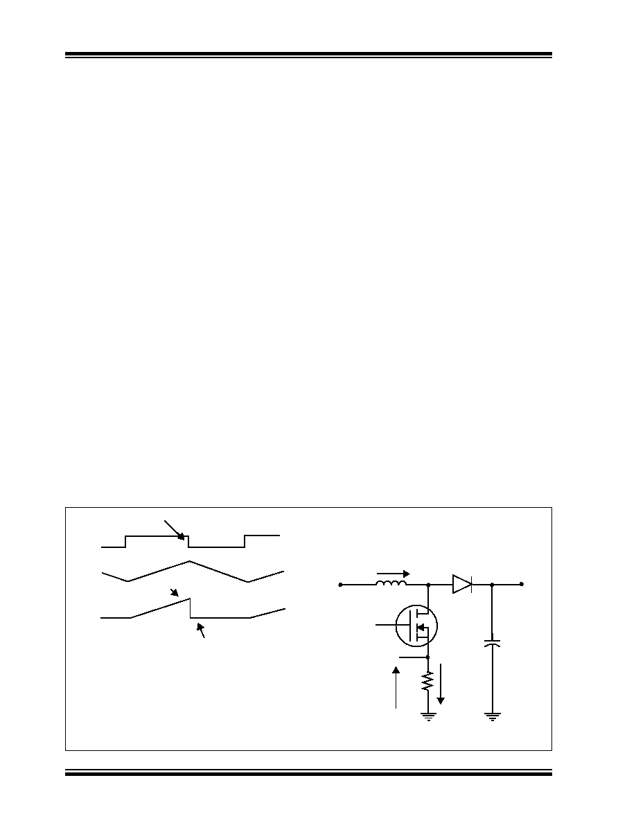
dsPIC30F1010/202X
DS70178A-page 176
Advance Information
©
2006 Microchip Technology Inc.
16.4
ADC Result Buffer
The ADC module contains up to 12 data output regis-
ters to store the A/D results called ADBUF<11:0>. The
registers are 10 bits wide, but are read into different
format, 16-bit words. The buffers are read-only.
Each analog input has a corresponding data
output register.
This module DOES NOT include a circular data
buffer or FIFO. Because the conversion results may
be produced in any order, such schemes will not work
since there would be no means to determine which
data is in a specific location.
The SAR write to the buffers is synchronous to the
ADC clock. Reads from the buffers will always have
valid data assuming that the data-ready interrupt has
been processed.
If a buffer location has not been read by the software
and the SAR needs to overwrite that location, the
previous data is lost.
Reads from the result buffer pass through the data for-
matter. The 10 bits of the result data are formatted into
a 16-bit word.
16.5
Application Information
The ADC module implements a concept based on
"Conversion Pairs". In power conversion applications,
there is a need to measure voltages and currents for
each PWM control loop. The ADC module enables the
sample and conversion process of each conversion
pair to be precisely timed relative to the PWM signals.
In a user's application circuit, the PWM signal enables
a transistor, which allows an inductor to charge up with
current to a desired value. The longer a PWM signal is
on, the longer the inductor is charging, and therefore
the inductor current is at its maximum at the end of the
PWM signal. Often, this is the point where the user
wants to take the current and voltage measurements.
Figure 16-2 shows a typical power conversion applica-
tion (a boost converter) where the current sensing of
the inductor is done by monitoring the voltage across a
resistor in series with the power transistor that
"charges" the inductor. The significant feature of this
figure is that if the sampling of the resistor voltage
occurs slightly later than the desired sample point, the
data read will be zero. This is not acceptable in most
applications. The ADC module always samples the
analog voltages at the appointed time regardless of
whether the ADC converter is busy or not.
The Power Supply PWM module supports 2-4 indepen-
dent PWM channels as well as 2-4 trigger signals (one
per PWM generator). The user can configure these
channels to initiate an ADC conversion of a selected
input pair at the proper time in the PWM cycle. The
Power Supply PWM module also provides an addi-
tional trigger signal (Special Event Trigger), which can
be programmed to occur at a specified time during the
primary time base count cycle.
FIGURE 16-2:
APPLICATION EXAMPLE: IMPORTANCE OF PRECISE SAMPLING
X
PWM
I
L
I
R
X
X
Late sample yields
zero data
Desired sample point
Critical Edge
+V
IN
I
L
L
PWM
V
ISENSE
V
OUT
C
OUT
+
I
R
R
Measuring peak inductor current is very important
Example Boost Converter

©
2006 Microchip Technology Inc.
Advance Information
DS70178A-page 177
dsPIC30F1010/202X
16.6
Reverse Conversion Order
The ORDER control bit in the ADCON register, when
set, reverses the order of the input pair conversion pro-
cess. Normally (ORDER
= 0
), the even numbered
input of an input pair is converted first, and then the odd
numbered input is converted. If ORDER
= 1
, the odd
numbered input pin of an input pair is converted first,
followed by the even numbered pin.
This feature is useful when using voltage control
modes and using the early interrupt capability
(EIE
= 1
). These features enable the user to minimize
the time period from actual acquisition of the feedback
(ADC) data to the update of the control output (PWM).
This time from input to output of the control system
determines the overall stability of the control system.
16.7
Simultaneous & Sequential
Sampling in a pair
The inputs that have dedicated Sample and Hold
(S&H) circuits are sampled when their specified trigger
events occur. The inputs that share the common sam-
ple and hold circuit are sampled in the following
manner:
1.
If the SEQSAMP bit =
0
, and the common
(shared) sample and hold circuit is NOT busy,
then the shared S&H will sample their specified
input at the same time as the dedicated S&H.
This action provides "Simultaneous" sample and
hold functionality.
2.
If the SEQSAMP bit =
0
, and the shared S&H is
currently busy with a conversion in progress,
then the shared S&H will sample as soon as
possible (at the start of the new conversion
process for the pair).
3.
If the SEQSAMP bit =
1
, then the shared S&H
will sample at the start of the conversion process
for that input. For example: If the ORDER bit =
0
the shared S&H will sample at the start of the
conversion of the second input. If ORDER =
1
,
then the shared S&H will sample at the start of
the conversion for the first input.
The SEQSAMP bit is useful for some applica-
tions that want to minimize the time from a
sample event to the conversion of the sample.
When SEQSAMP =
0
, the logic attempts to take
the samples for both inputs of a pair at the same
time if the resources are available. The user can
often ensure that the ADC will not be busy with
a prior conversion by controlling the timing of the
trigger signals that initiate the conversion
processes.
16.8
Group Interrupt Generation
The ADC module provides a common or "Group" inter-
rupt request that is the OR of all of the enabled interrupt
sources within the module. Each CPC register has two
IRQENx bits, one for each analog input pair. If the
IRQEN bit is set, an interrupt request is made to the
interrupt controller when the requested conversion is
completed. When an interrupt is generated, an asso-
ciated PxRDY bit in the ADSTAT register is set. The
PxRDY bit is cleared by the user. The user's software
can examine the ADSTAT register's PxRDY bits to
determine if additional requested conversions have
been completed.
The group interrupt is useful for applications that use a
common software routine to process ADC interrupts for
multiple analog input pairs. This method is more
traditional in concept.
Note:
The user must clear the IFS bit associated
with the ADC in the interrupt controller
before the PxRDY bit is cleared. Failure to
do so may cause interrupts to be lost. The
reason is that the ADC will possibly have
another interrupt pending. If the user
clears the PxRDY bit first, the ADC may
generate another interrupt request, but if
the user then clears the IFS bit, the
interrupt request will be erased.

dsPIC30F1010/202X
DS70178A-page 178
Advance Information
©
2006 Microchip Technology Inc.
16.9
Individual Pair Interrupts
The ADC module also provides individual interrupts
outputs for each analog input pair. These interrupts are
always enabled within the module. The pair interrupts
can be individually enabled or disabled via the
associated Interrupt Enable bits in the IEC registers.
Using the group interrupts may require the interrupt
service routine to determine which interrupt source
generated the interrupt. For applications that use sep-
arate software tasks to process ADC data, a common
interrupt vector can cause performance bottlenecks.
The use of the individual pair interrupts can save many
clock cycles as compared to using the group interrupt
to process multiple interrupt sources. The individual
pair interrupts support the construction of application
software that is responsive and organized on a task
basis.
Regardless of whether an individual pair interrupt or the
global interrupt are used to respond to an interrupt
request from an ADC conversion, the PxRDY bits in the
ADSTAT register function in the same manner.
The use of the individual pair interrupts also enables
the user to change the interrupt priority of individual
ADC channels (pairs) as compared to the fixed priority
structure of the group interrupt.
NOTE: The use of individual interrupts DOES NOT
affect the priority structure of the ADC with respect
to the order of input pair conversion.
The use of individual interrupts can reduce the problem
of accidently "losing" a pending interrupt while process-
ing and clearing a current interrupt
16.10 Early Interrupt Generation
The EIE control bit in the ADCON register enables the
generation of the interrupts after completion of the first
conversion instead of waiting for the completion of both
inputs of an input pair. Even though the second input
will still be in the conversion process, the software can
be written to perform some of the computations using
the first data value while the second conversion is
completed.
The user software can be written to account for the 500
nsec conversion period of the second input before
using the second data, or the user can poll the PEND
bit in the CPCx register.
The PEND bit remains set until both conversions of a
pair have been completed. The PXRDY bit for the
associated interrupt is set in the ADSTAT register at the
completion of the first conversion, and remains set until
it is cleared by the user.
16.11 Conflict Resolution
If more than one conversion pair request is active at the
same time, the ADC control logic processes the
requests in a top-down manner, starting at analog pair
#0 (AN1/AN0) and ending at analog pair #5 (AN11/
AN10). This is not a "round-robin" process.
16.12 Deliberate Conflicts
If the user specifies the same conversion trigger source
for multiple "conversion pairs", then the ADC module
functions like other dsPIC30F ADC modules; i.e., it pro-
cesses the requested conversions
sequentially (in pairs) until the sequence has
been completed.
16.13 ADC Clock Selection
The ADCS<2:0> bits in the ADCON register specify the
clock divisor value for the ADC clock generation logic.
The input to the ADC clock divisor is the system clock
(240 MHz @ 30 MIPS) when the PLL is operating. This
high-frequency clock provides the needed timing reso-
lution to generate a 24 MHz ADC clock signal required
to process two ADC conversions in 1 microsecond.
Note:
The ADC module will NOT repeatedly loop
once triggered. Each sequence of
conversions requires a trigger or multiple
triggers.

©
2006 Microchip Technology Inc.
Advance Information
DS70178A-page 179
dsPIC30F1010/202X
16.14 ADC Base Register
It is expected that the user application may have the
ADC module generate 500,000 interrupts per second.
To speed the evaluation of the PxRDY bits in the
ADSTAT register, the ADC module features the read/
write register: ADBASE. When read, the ADBASE reg-
ister will provide a sum of the contents of the ADBASE
register plus an encoding of the PxRDY bits set in the
ADSTAT register.
The Least Significant bit of the ADBASE register is
forced to zero. This ensures that all (ADBASE +
PxRDY) results will be on instruction boundaries.
The PxRDY bits are binary priority encoded with
P0RDY being the highest priority, and P5RDY being
the lowest priority. The encoded priority result is then
shifted left two bit positions and added to the contents
of the ADBASE register. This means the priority
encoding yields addresses that are on two instruction
word boundaries.
The user will typically load the ADBASE register with
the base address of a "Jump" table that contains either
the addresses of the appropriate ISRs or branches to
the appropriate ISR. The encoded PxRDY values are
set up to reserve two instruction words per entry in the
Jump table. It is expected that the user software will
use one instruction word to load an identifier into a W
register, and the other instruction will be a branch to
the appropriate ISR.
16.15 Changing A/D Clock
In general, the A/D cannot accept changes to the ADC
clock divisor while ADON
= 1
. If the user makes A/D
clock changes while
ADON
= 1
, the results will be
indeterminate.
16.16 Sample and Conversion
The ADC module always assigns two ADC clock peri-
ods for the sampling process. When operating at the
maximum conversion rate of 2 Msps per channel, the
sampling period is:
2 x 41.6 nsec = 83.3 nsec.
Each ADC pair specified in the CPCx registers initiates
a sample operation when the selected trigger event
occurs. The conversion of the sampled analog data
occurs as resources become available.
If a new trigger event occurs for a specific channel
before a previous sample and convert request for that
channel has been processed, the newer request is
ignored. It is the user's responsibility not to exceed the
conversion rate capability for the module.
The actual conversion process requires 10 additional
ADC clocks. The conversion is processed serially, bit 9
first, then bit 8, down to bit 0. The result is stored when
the conversion is completed.
16.17 A/D Sample and Convert Timing
The sample and hold circuits assigned to the input
pins have their own timing logic that is triggered when
an external sample and convert request (from PWM or
TMR) is made. The sample and hold circuits have a
fixed two clock data sample period. When the sample
has been acquired, then the ADC control logic is
notified of a pending request, then the conversion is
performed as the conversion resources become
available.
The ADC module always converts pairs of analog
input channels, so a typical conversion process
requires 24 clock cycles.
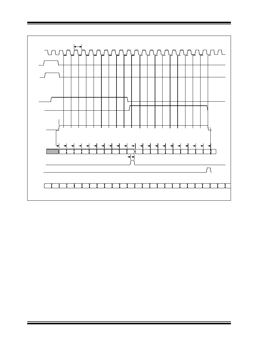
dsPIC30F1010/202X
DS70178A-page 180
Advance Information
©
2006 Microchip Technology Inc.
FIGURE 16-3:
DETAILED CONVERSION SEQUENCE TIMINGS, SEQSAMP =
0
, NOT BUSY
10th
9th
8th
7th
6th
5th
4th
3rd
2nd 1st
T
AD
adc_clk
sample_even
convert_en
capture_first_data
10th
9th
8th
7th
6th
5th
4th
3rd
2nd 1st
4
5
6
7
8
9
10
11
12
13
14
15
16
17
18
19
20
21
0
1
2
0
1
2
3
connect_second
connect_first
state counter
capture_second_data
sample_odd
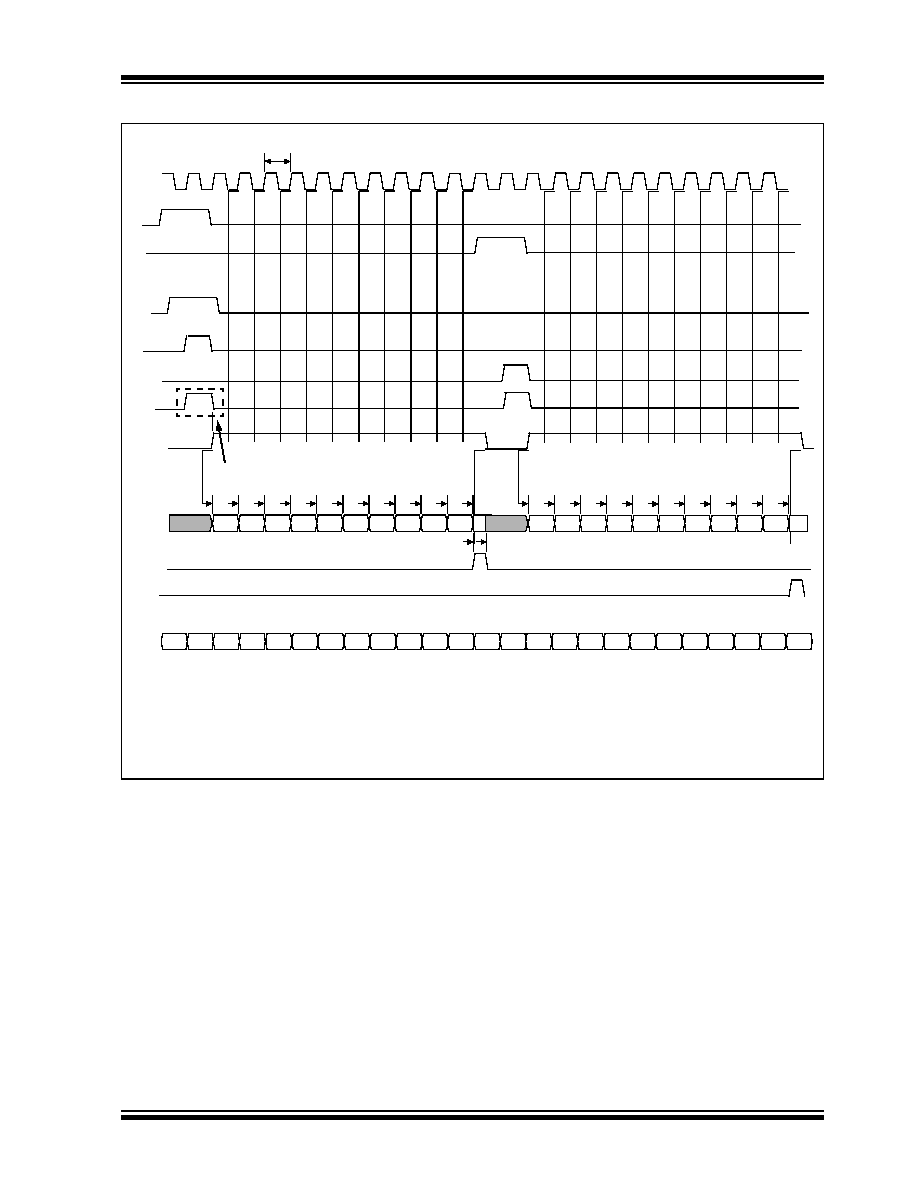
©
2006 Microchip Technology Inc.
Advance Information
DS70178A-page 181
dsPIC30F1010/202X
FIGURE 16-4:
DETAILED CONVERSION SEQUENCE TIMINGS, SEQSAMP =
1
10th
9th
8th
7th
6th
5th
4th
3rd
2nd 1st
T
AD
adc_clk
sample_even
convert_en
capture_first_data
10th
9th
8th
7th
6th
5th
4th
3rd
2nd 1st
4
5
6
7
8
9
10
11
12
13
14
15
16
17
18
19
20
21
22
23
0
0
1
2
3
sample_odd
(1)
connect_second
connectx_en
state counter
capture_second_data
connect_common
sample_odd
(2)
Dependent on S&H availability
Note 1:
For all analog input pairs that do not have dedicated sample and hold circuits, the common sample and hold circuit
samples the input at the start of the first and second conversions. Therefore, the samples are sequential, not
simultaneous.
2:
For all analog input pairs that have dedicated sample and hold circuits, the common sample and hold circuit samples
the input at the start of the first conversion so that both samples (odd and even) are near simultaneous.
dsPIC30F1010/202X
DS70178A-page 182
Advance Information
©
2006 Microchip Technology Inc.
16.18 Module Power-Down Modes
The module has two internal power modes.
When the ADON bit is `
1
', the module is in Active mode
and is fully powered and functional.
When ADON is `
0
', the module is in Off mode. The state
machine for the module is reset, as are all of the
pending conversion requests.
To return to the Active mode from Off mode, the user
must wait for the bias generators to stabilize. The
stabilization time is specified in the electrical specs.
16.19 Effects of a Reset
A device reset forces all registers to their reset state.
This forces the A/D module to be turned off, and any
conversion and sampling sequence is aborted. The
value that is in the ADBUFx register is not modified.
The ADBUFx registers contain unknown data after a
Power-on Reset.
16.20 Configuring Analog Port Pins
The use of the ADPCFG and TRIS registers control the
operation of the A/D port pins.
The port pins that are desired as analog inputs should
have their corresponding TRIS bit set (input). If the
TRIS bit is cleared (output), the digital output level (V
OH
or V
OL
) will be converted.
Port pins that are desired as analog inputs must have
the corresponding ADPCFG bit clear. This will config-
ure the port to disable the digital input buffer. Analog
levels on pins where ADPCFG<n>
= 1
, may cause the
digital input buffer to consume excessive current.
If a pin is not configured as an analog input
ADPCFG<n>
= 1
, the analog input is forced to AVss
and conversions of that input do not yield meaningful
results.
When reading the PORT register, all pins configured as
analog input ADPCFG<n>
= 0
, will read `
0
'.
The A/D operation is independent of the state of the
input selection bits and the TRIS bits.
Some devices may have analog inputs multiplexed with
A/D voltage reference inputs V
REF
- and V
REF
+. This
does not affect the functionality of these pins. The user
may still specify those pins as analog inputs and
convert them, the results will either be 0x000 or 0xFFF.
16.21 Output Formats
The A/D converts 10 bits. The data buffer RAM is 16
bits wide. The ADC data can be read in one of two dif-
ferent formats, as shown in Figure 16-5. The FORM bit
selects the format. Each of the output formats
translates to a 16-bit result on the data bus.
FIGURE 16-5:
A/D OUTPUT DATA FORMAT
RAM contents:
d09 d08 d07 d06 d05 d04 d03 d02 d01
d00
Read to Bus:
Fractional
d09
d08 d07
d06
d05 d04 d03 d02 d01 d00 0
0
0
0
0
0
Integer
0
0
0
0
0
0
d09 d08 d07 d06 d05 d04 d03 d02 d01
d00

©
2006 Microchip Technology Inc.
Advance Information
DS70178A-page 183
dsPIC30F1010/202X
T
A
BLE
1
6
-8:
ADC RE
GIS
T
E
R
M
A
P
F
ile
Na
m
e
ADR
Bit
1
5
Bit
1
4
Bit
1
3
Bi
t
1
2
Bit
1
1
Bit
1
0
Bit
9
B
it
8
B
it
7
B
i
t
6
B
it 5
B
it
4
B
it
3
B
it
2
B
it 1
B
i
t
0
A
l
l
Res
e
t
s
A
DCO
N
030
0
A
D
O
N
--A
D
S
I
D
L
--
--G
S
W
T
R
G
--
F
ORM
E
IE
O
RDE
R
S
E
Q
S
A
M
P
--
--
A
DCS<2
:
0
>
0009
AD
P
C
F
G
1
030
2
--
--
--
--
P
C
F
G
1
1
P
CF
G
1
0
P
CF
G9
PCF
G
8
P
CF
G
7
PCF
G
6
P
CF
G5
PCF
G
4
P
CF
G
3
PCF
G
2
P
C
F
G1
PCF
G
0
0000
Re
se
r
v
e
d
030
4
--
--
--
--
--
--
--
--
--
--
--
--
--
--
--
--
0000
AD
S
T
A
T
030
6
--
--
--
--
--
--
--
--
--
--
P
5
R
DY
P4
R
D
Y
P
3
RDY
P2
RDY
P
1
RDY
P0
RDY
0000
A
D
BASE
030
8
ADBASE<1
5
:
1
>
--
0000
A
DCPC0
0
3
0
A
I
RQEN1
PEND1
SWT
R
G
1
T
R
GSRC1
<5
:0
>
I
RQEN
0
PEND0
SWT
R
G
0
T
R
GSRC0
<5
:0
>
0000
A
DCPC1
0
3
0
C
IRQEN3
PEND3
SWT
R
G
3
T
R
GSRC3
<5
:0
>
I
RQEN
2
PEND2
SWT
R
G
2
T
R
GSRC2
<5
:0
>
0000
A
DCPC2
0
3
0
E
I
RQEN5
PEND5
SWT
R
G
5
T
R
GSRC5
<5
:0
>
I
RQEN
4
PEND4
SWT
R
G
4
T
R
GSRC4
<5
:0
>
0000
Re
se
r
v
e
d
03
10 ≠
03
1E
---
--
--
--
--
--
--
--
--
--
--
--
--
--
--
--
0000
A
DCBUF
0
0
320
--
--
--
--
--
--
A
DC Da
ta
Bu
f
f
e
r
0
xxxx
A
DCBUF
1
0
322
--
--
--
--
--
--
A
DC Da
ta
Bu
f
f
e
r
1
xxxx
A
DCBUF
2
0
324
--
--
--
--
--
--
A
DC Da
ta
Bu
f
f
e
r
2
xxxx
A
DCBUF
3
0
326
--
--
--
--
--
--
A
DC Da
ta
Bu
f
f
e
r
3
xxxx
A
DCBUF
4
0
328
--
--
--
--
--
--
A
DC Da
ta
Bu
f
f
e
r
4
xxxx
A
DCBUF
5
032
A
--
--
--
--
--
--
A
DC Da
ta
Bu
f
f
e
r
5
xxxx
A
DCBUF
6
03
2C
--
--
--
--
--
--
A
DC Da
ta
Bu
f
f
e
r
6
xxxx
A
DCBUF
7
032
E
--
--
--
--
--
--
A
DC Da
ta
Bu
f
f
e
r
7
xxxx
A
DCBUF
8
0
330
--
--
--
--
--
--
A
DC Da
ta
Bu
f
f
e
r
8
xxxx
A
DCBUF
9
0
332
--
--
--
--
--
--
A
DC Da
ta
Bu
f
f
e
r
9
xxxx
A
DCBUF
1
0
0
334
--
--
--
--
--
--
A
D
C
Data B
u
ffer
10
xxxx
A
DCBUF
1
1
0
336
--
--
--
--
--
--
A
DC Da
ta
Bu
f
f
e
r
1
1
xxxx
Re
se
r
v
e
d
03
38 ≠
037
E
--
--
--
--
--
--
--
--
--
--
--
--
--
--
--
--
0000

dsPIC30F1010/202X
DS70178A-page 184
Advance Information
©
2006 Microchip Technology Inc.
NOTES:
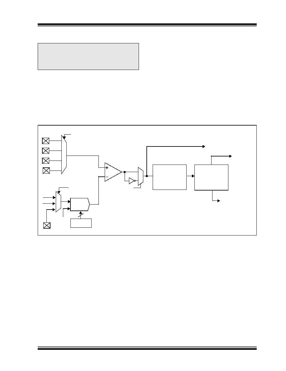
©
2006 Microchip Technology Inc.
Advance Information
DS70178A-page 185
dsPIC30F1010/202X
17.0
SMPS COMPARATOR MODULE
The dsPIC30F SMPS Comparator module monitors
current and/or voltage transients that may be too fast
for the CPU and ADC to capture.
17.1
Features Overview
∑ 16 comparator inputs
∑ 10-bit DAC provides reference
∑ Programmable output polarity
∑ Interrupt generation capability
∑ Selectable Input sources
∑ DAC has three ranges of operation
- AV
DD
/ 2
- Internal Reference 1.2V 1%
- External Reference < (AV
DD
≠ 1.6V)
∑ ADC sample and convert trigger capability
∑ Can be disabled to reduce power consumption
∑ Functional support for PWM Module:
- PWM Duty Cycle Control
- PWM Period Control
- PWM Fault Detect
FIGURE 17-1:
COMPARATOR MODULE BLOCK DIAGRAM
17.2
Module Applications
This module provides a means for the SMPS dsPIC
DSC devices to monitor voltage and currents in a
power conversion application. The ability to detect
transient conditions and stimulate the dsPIC DSC pro-
cessor and/or peripherals without requiring the proces-
sor and ADC to constantly monitor voltages or currents
frees the dsPIC DSC to perform other tasks.
The Comparator module has a high-speed comparator
and an associated 10-bit DAC that provides a pro-
grammable reference voltage to one input of the com-
parator. The polarity of the comparator output is user
programmable. The output of the module can be used
in the following modes:
∑ Generate an interrupt
∑ Trigger an ADC sample and convert process
∑ Truncate the PWM signal (current limit)
∑ Truncate the PWM period (current minimum)
∑ Disable the PWM outputs (Fault-latch)
The output of the Comparator module may be used in
multiple modes at the same time, such as: (1) gener-
ate an interrupt, (2) have the ADC take a sample and
convert it and (3) truncate the PWM output in
response to a voltage being detected beyond its
expected value.
The Comparator module can also be used to wake-up
the system from Sleep or Idle mode when the analog
input voltage exceeds the programmed threshold
voltage.
Note: This data sheet summarizes features of this group
of dsPIC30F devices and is not intended to be a complete
reference source. For more information on the CPU,
peripherals, register descriptions and general device
functionality, refer to the "dsPIC30F Family Reference
Manual" (DS70046).
CMP
x
A*
CMP
x
C*
DAC
CMPPOL
0
1
AV
DD
/2
V
REF
A
VSS
M
U
X
CMREF
CMP
x
*
RANGE
INSEL<1:0>
10
Trigger to PWM
Interrupt Request
CMP
x
B*
CMP
x
D*
Glitch Filter
Pulse Generator
Status
EXTREF
M
U
X
* x=1, 2, 3 & 4

dsPIC30F1010/202X
DS70178A-page 186
Advance Information
©
2006 Microchip Technology Inc.
17.3
Module Description
The Comparator module uses a 20 nsec comparator.
The comparator offset is ±5 mV typical. The negative
input of the comparator is always connected to the
DAC circuit. The positive input of the comparator is
connected to an analog multiplexer that selects the
desired source pin.
17.4
DAC
The range of the DAC is controlled via an analog mul-
tiplexer that selects either AV
DD
/ 2, internal 1.2V 1%
reference, or an external reference source EXTREF.
The full range of the DAC (AV
DD
/ 2) will typically be
used when the chosen input source pin is shared with
the ADC. The reduced range option (V
REF
) will likely
be used when monitoring current levels via a CLx pin
using a current sense resistor. Usually, the measured
voltages in such applications are small (<1.25V),
therefore the option of using a reduced reference
range for the comparator extends the available DAC
resolution in these applications. The use of an external
reference enables the user to connect to a reference
that better suits their application.
17.5
Interaction with I/O Buffers
If the comparator module is enabled and a pin has
been selected as the source for the comparator, then
the chosen I/O pad must disable the digital input buffer
associated with the pad to prevent excessive currents
in the digital buffer due to analog input voltages.
17.6
Digital Logic
The CMPCONx register (see Register 17-1) provides
the control logic that configures the Comparator mod-
ule. The digital logic provides a glitch filter for the com-
parator output to mask transient signals less than two
T
CY
(66 nsec) in duration. In Sleep or Idle mode, the
glitch filter is bypassed to enable an asynchronous
path from the comparator to the interrupt controller.
This asynchronous path can be used to wake-up the
processor from Sleep or Idle mode.
The comparator can be disabled while in Idle mode if
the CMPSIDL bit is set. If a device has multiple com-
parators, if any CMPSIDL bit is set, then the entire
group of comparators will be disabled while in Idle
mode. This behavior reduces complexity in the design
of the clock control logic for this module.
The digital logic also provides a one T
CY
width pulse
generator for triggering the ADC and generating
interrupt requests.
The CMPDACx (see Register 17-2) register provides
the digital input value to the reference DAC.
If the module is disabled, the DAC and comparator are
disabled to reduce power consumption.
17.7
Comparator Input Range
The comparator has a limitation for the input Common
Mode Range (CMR) of about 3.5 volts (AV
DD
≠ 1.5
volts). This means that both inputs should not exceed
this value or the comparator's output will become inde-
terminent. As long as one of the inputs is within the
Common Mode Range, the comparator output will be
correct. An input excursion into the CMR region will
not corrupt the comparator output, but the comparator
input is saturated.
17.8
DAC Output Range
The DAC has a limitation for the maximum reference
voltage input of (AV
DD
≠ 1.6) volts. An external refer-
ence voltage input should not exceed this value or the
reference DAC output will become indeterminate.
17.9
Comparator Registers
The Comparator module is controlled by the following
registers:
∑ Comparator Control Registerx (CMPCONx)
∑ Comparator DAC Control Registerx (CMPDACx)

©
2006 Microchip Technology Inc.
Advance Information
DS70178A-page 187
dsPIC30F1010/202X
REGISTER 17-1:
COMPARATOR CONTROL REGISTER
X
(CMPCONx)
R/W-0
U-0
R/W-0
U-0
U-0
U-0
U-0
U-0
CMPON
--
CMPSIDL
--
--
--
--
--
bit 15
bit 8
R/W-0
R/W-0
R/W-0
U-0
R/W-0
U-0
R/W-0
R/W-0
INSEL<1:0>
EXTREF
--
CMPSTAT
--
CMPPOL
RANGE
bit 7
bit 0
Legend:
R = Readable bit
W = Writable bit
U = Unimplemented bit, read as `0'
-n = Value at POR
`1' = Bit is set
`0' = Bit is cleared
x = Bit is unknown
bit 15
CMPON: A/D Operating Mode bit
1
= Comparator module is enabled
0
= Comparator module is disabled (reduces power consumption)
bit 14
Unimplemented: Read as `
0
'
bit 13
CMPSIDL: Stop in Idle Mode bit
1
= Discontinue module operation when device enters Idle mode.
0
= Continue module operation in Idle mode.
If a device has multiple comparators, any CMPSIDL bit set to `
1
' disables ALL comparators while in
Idle mode.
bit 12-8
Reserved: Read as `
0
'
bit 7-6
INSEL<1:0>: Input Source Select for Comparator bits
00
= Select CMPxA input pin
01
= Select CMPxB input pin
10
= Select CMPxC input pin
11
= Select CMPxD input pin
bit 5
EXTREF: Enable External Reference bit
1
= External source provides reference to DAC
0
= Internal reference sources provide source to DAC
bit 4
Reserved: Read as `
0
'
bit 3
CMPSTAT: Current State of Comparator Output Including CMPPOL Selection bit
bit 2
Reserved: Read as `
0
'
bit 1
CMPPOL: Comparator Output Polarity Control bit
1
= Output is inverted
0
= Output is non inverted
bit 0
RANGE: Selects DAC Output Voltage Range bit
1
= High Range: Max DAC value = AV
DD
/ 2, 2.5V @ 5 volt V
DD
0
= Low Range: Max DAC value = Internal Reference, 1.2V +-1%

dsPIC30F1010/202X
DS70178A-page 188
Advance Information
©
2006 Microchip Technology Inc.
REGISTER 17-2:
COMPARATOR DAC CONTROL REGISTER
X
(CMPDACx)
U-0
U-0
U-0
U-0
U-0
U-0
R/W-0
R/W-0
--
--
--
--
--
--
CMREF<9:8>
bit 15
bit 8
R/W-0
R/W-0
R/W-0
R/W-0
R/W-0
R/W-0
R/W-0
R/W-0
CMREF<7:0>
bit 7
bit 0
Legend:
R = Readable bit
W = Writable bit
U = Unimplemented bit, read as `0'
-n = Value at POR
`1' = Bit is set
`0' = Bit is cleared
x = Bit is unknown
bit 15-10
Reserved: Read as `
0
'
These bits are reserved for possible future expansion of the DAC from 10 bits to more bits.
bit 9-0
CMREF<9:0>: Comparator Reference Voltage Select bits
1111111111
= (CMREF * V
REF
/ 1024) or (CMREF * AV
DD
/ 1024) volts depending on Range bit
∑∑∑∑∑
0000000000
= 0.0 volts

©
2006 Microchip Technology Inc.
Advance Information
DS70178A-page 189
dsPIC30F1010/202X
T
A
BLE
1
7
-3:
ANALOG COMP
A
RATO
R
CONTROL RE
GIS
T
E
R
MAP
F
i
l
e
Na
m
e
AD
R
B
it
1
5
Bit
1
4
Bit
1
3
Bit
1
2
Bi
t
1
1
Bit
1
0
Bit
9
B
it
8
B
it 7
B
it 6
B
it
5
B
it 4
B
it
3
B
it
2
B
it
1
B
it
0
A
ll
R
ese
t
s
CM
PCON1
0
4
C
0
CM
PON
--
CM
PSIDL
--
--
--
--
--
I
N
SEL
<1
:
0
>
EXTRE
F
--
C
M
PST
A
T
--
CM
PPO
L
R
ANG
E
00
00
CM
PDAC1
0
4
C
2
--
--
--
--
--
--
CM
RE
F
<
9
:
0
>
00
00
CM
PCON
2
0
4
C
4
CM
PON
--
CM
PSIDL
--
--
--
--
--
I
N
SEL
<1
:
0
>
EXTRE
F
--
C
M
PST
A
T
--
CM
PPO
L
R
ANG
E
00
00
CM
PDAC2
0
4
C
6
--
--
--
--
--
--
CM
RE
F
<
9
:
0
>
00
00
CM
PCON
3
0
4
C
8
CM
PON
--
CM
PSIDL
--
--
--
--
--
I
N
SEL
<1
:
0
>
EXTRE
F
--
C
M
PST
A
T
--
CM
PPO
L
R
ANG
E
00
00
CM
PDAC3
0
4
C
A
--
--
--
--
--
--
CM
RE
F
<
9
:
0
>
00
00
CM
PCON
4
0
4
C
C
CM
PON
--
CM
PSIDL
--
--
--
--
--
I
N
SEL
<1
:
0
>
EXTRE
F
--
C
M
PST
A
T
--
CM
PPO
L
R
ANG
E
00
00
CM
PDAC4
0
4
C
E
--
--
--
--
--
--
CM
RE
F
<
9
:
0
>
00
00

dsPIC30F1010/202X
DS70178A-page 190
Advance Information
©
2006 Microchip Technology Inc.
NOTES:

©
2006 Microchip Technology Inc.
Advance Information
DS70178A-page 191
dsPIC30F1010/202X
18.0
SYSTEM INTEGRATION
There are several features intended to maximize sys-
tem reliability, minimize cost through elimination of
external components, provide power-saving operating
modes and offer code protection:
∑ Oscillator Selection
∑ Reset:
- Power-on Reset (POR)
- Power-up Timer (PWRT)
- Oscillator Start-up Timer (OST)
∑ Watchdog Timer (WDT)
∑ Power-Saving modes (Sleep and Idle)
∑ Code Protection
∑ Unit ID Locations
∑ In-Circuit Serial Programming (ICSP)
programming capability
dsPIC30F devices have a Watchdog Timer, which can
be permanently enabled via the Configuration bits or
can be software controlled. It runs off its own RC oscil-
lator for added reliability. There are two timers that offer
necessary delays on power-up. One is the Oscillator
Start-up Timer (OST), intended to keep the chip in
Reset until the crystal oscillator is stable. The other is
the Power-up Timer (PWRT), which provides a delay
on power-up only, designed to keep the part in Reset
mode while the power supply stabilizes. With these two
timers on-chip, most applications need no external
Reset circuitry.
Sleep mode is designed to offer a very low-current
Power-Down mode. The user can wake-up from Sleep
mode through external Reset, Watchdog Timer Wake-
up or through an interrupt. Several oscillator options
are also made available to allow the part to fit a wide
variety of applications. In the Idle mode, the clock
sources are still active, but the CPU is shut off. The RC
oscillator option saves system cost, while the LP crystal
option saves power.
18.1
Oscillator System Overview
The dsPIC30F oscillator system has the following
modules and features:
∑ Various external and internal oscillator options as
clock sources
∑ An on-chip PLL to boost internal operating
frequency
∑ A clock switching mechanism between various
clock sources
∑ Programmable clock postscaler for system power
savings
∑ A Fail-Safe Clock Monitor (FSCM) that detects
clock failure and takes fail-safe measures
∑ Clock Control register OSCCON
∑ Configuration bits for main oscillator selection
Configuration bits determine the clock source upon
Power-on Reset (POR). Thereafter, the clock source
can be changed between permissible clock sources.
The OSCCON register controls the clock switching and
reflects system clock related status bits.
Table 18-1 provides a summary of the dsPIC30F oscil-
lator operating modes. A simplified diagram of the
oscillator system is shown in Figure 18-1.
18.2
Oscillator Control REGISTERS
The oscillators are controlled with OSCCON, OSC-
TUN, OSCTUN2, FOSC and the FOSCSEL registers.
Note: This data sheet summarizes features of this group
of dsPIC30F devices and is not intended to be a complete
reference source. For more information on the CPU,
peripherals, register descriptions and general device
functionality, refer to the "dsPIC30F Family Reference
Manual" (DS70046).
For more information on the device instruction set and pro-
gramming, refer to the "dsPIC30F/33F Programmer's
Reference Manual" (DS70157).
Note: 32 kHz crystal operation is not enabled on
dsPIC30F1010/202X devices.
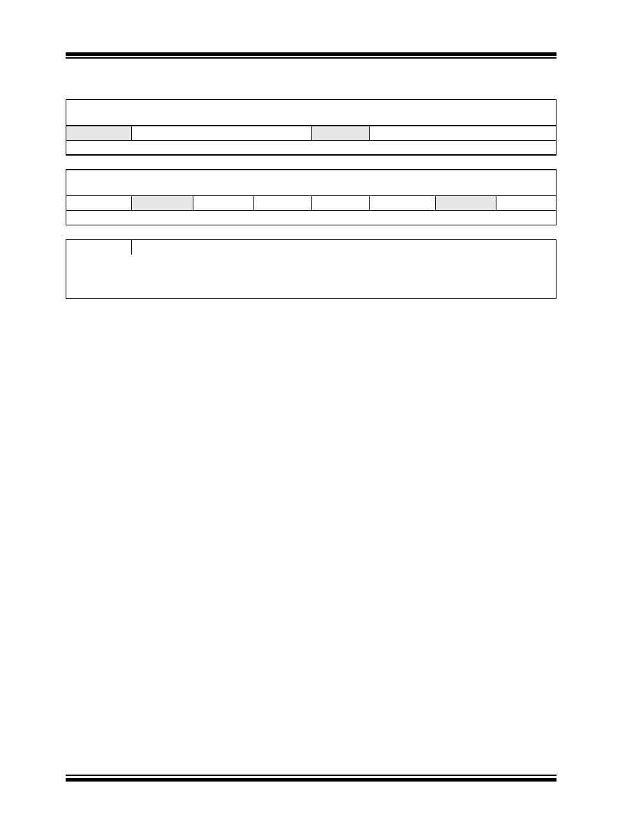
dsPIC30F1010/202X
DS70178A-page 192
Advance Information
©
2006 Microchip Technology Inc.
REGISTER 18-1:
OSCCON: OSCILLATOR CONTROL REGISTER
U-0
R-y
HS,HC
R-y
HS,HC
R-y
HS,HC
U-0
R/W-y
R/W-y
R/W-y
--
COSC<2:0>
--
NOSC<2:0>
bit 15
bit 8
R/W-0
U-0
R-0
HS,HC
R/W-0
R/C-0
HS,HC
R/W-0
U-0
R/W-0
HC
CLKLOCK
--
LOCK
PRCDEN
CF
TSEQEN
--
OSWEN
bit 7
bit 0
Legend:
x = Bit is unknown
R = Readable bit
W = Writable bit
U = Unimplemented bit, read as `0'
-n = Value at POR
HC = Cleared by hardware
`1' = Bit is set
HS = Set by hardware
`0' = Bit is cleared
-y = Value set from Configuration bits on POR
bit 15
Unimplemented: Read as `
0
'
bit 14-12
COSC<2:0>: Current Oscillator Group Selection bits (read-only)
000
= Fast RC Oscillator (FRC)
001
= Fast RC Oscillator (FRC) with PLL Module
010
= Primary Oscillator (HS, EC)
011
= Primary Oscillator (HS, EC) with PLL Module
100
= Reserved
101
= Reserved
110
= Reserved
111
= Reserved
This bit is Reset upon:
Set to FRC value (`
000
') on POR
Loaded with NOSC<2:0> at the completion of a successful clock switch
Set to FRC value (`
000
') when FSCM detects a failure and switches clock to FRC
bit 11
Unimplemented: Read as `
0
'
bit 10-8
NOSC<2:0>: New Oscillator Group Selection bits
000
= Fast RC Oscillator (FRC)
001
= Fast RC Oscillator (FRC) with PLL Module
010
= Primary Oscillator (HS, EC)
011
= Primary Oscillator (HS, EC) with PLL Module
100
= Reserved
101
= Reserved
110
= Reserved
111
= Reserved
bit 7
CLKLOCK: Clock Lock Enabled bit
1
= If (FCKSM1 =
1
), then clock and PLL configurations are locked
If (FCKSM1 =
0
), then clock and PLL configurations may be modified
0
= Clock and PLL selection are not locked, configurations may be modified
Note:
Once set, this bit can only be cleared via a Reset.
bit 6
Unimplemented: Read as `
0
'

©
2006 Microchip Technology Inc.
Advance Information
DS70178A-page 193
dsPIC30F1010/202X
bit 5
LOCK: PLL Lock Status bit (read-only)
1
= Indicates that PLL is in lock
0
= Indicates that PLL is out of lock (or disabled)
This bit is Reset upon:
Reset on POR
Reset when a valid clock switching sequence is initiated by the clock switch state machine
Set when PLL lock is achieved after a PLL start
Reset when lock is lost
Read zero when PLL is not selected as a Group 1 system clock
bit 4
PRCDEN: Pseudo Random Clock Dither Enable bit
1
= Pseudo random clock dither is enabled
0
= Pseudo random clock dither is disabled.
bit 3
CF: Clock Fail Detect bit (read/clearable by application)
1
= FSCM has detected clock failure
0
= FSCM has NOT detected clock failure
This bit is Reset upon:
Reset on POR
Reset when a valid clock switching sequence is initiated by the clock switch state machine
Set when clock fail detected
bit 2
TSEQEN: FRC Tune Sequencer Enable bit
1
= The TUN<3:0>, TSEQ1<3:0>,
...
, TSEQ7<3:0> bits in the OSCTUN and the OSCTUN2 regis-
ters sequentially tune the FRC oscillator. Each field being sequentially selected via the
ROLL<2:0> signals from the PWM module.
0
= The TUN<3:0> bits in OSCTUN register tunes the FRC oscillator.
bit 1
Unimplemented: Read as `
0
'
bit 0
OSWEN: Oscillator Switch Enable bit
1
= Request oscillator switch to selection specified by NOSC<1:0> bits
0
= Oscillator switch is complete
This bit is Reset upon:
Reset on POR
Reset after a successful clock switch
Reset after a redundant clock switch
Reset after FSCM switches the oscillator to (Group 3) FRC
REGISTER 18-1:
OSCCON: OSCILLATOR CONTROL REGISTER (CONTINUED)

dsPIC30F1010/202X
DS70178A-page 194
Advance Information
©
2006 Microchip Technology Inc.
REGISTER 18-2:
OSCTUN: OSCILLATOR TUNING REGISTER
R/W-0
R/W-0
R/W-0
R/W-0
R/W-0
R/W-0
R/W-0
R/W-0
TSEQ3<3:0>
TSEQ2<3:0>
bit 15
bit 8
R/W-0
R/W-0
R/W-0
R/W-0
R/W-0
R/W-0
R/W-0
R/W-0
TSEQ1<3:0>
TUN<3:0>
bit 7
bit 0
Legend:
R = Readable bit
W = Writable bit
U = Unimplemented bit, read as `0'
-n = Value at POR
`1' = Bit is set
`0' = Bit is cleared
x = Bit is unknown
bit 15-12
TSEQ3<3:0>: Tune Sequence Value #3 bits
When PWM ROLL<2:0> =
011
, this field is used to tune the FRC instead of TUN<3:0>
bit 11-8
TSEQ2<3:0>: Tune Sequence Value #2 bits
When PWM ROLL<2:0> =
010
, this field is used to tune the FRC instead of TUN<3:0>
bit 7-4
TSEQ1<3:0>: Tune Sequence Value #1 bits
When PWM ROLL<2:0> =
001
, this field is used to tune the FRC instead of TUN<3:0>
bit 3-0
TUN<3:0>: Specifies the user tuning capability for the internal fast RC oscillator (nominal 15.0 MHz).
If the TSEQEN bit in the OSCCON register is set, this field, along with bits TSEQ1-TSEQ7, will
sequentially tune the FRC oscillator.
0111
= Maximum frequency
0110
=
0101
=
0100
=
0011
=
0010
=
0001
=
0000
= Center frequency, oscillator is running at calibrated frequency
1111
=
1110
=
1101
=
1100
=
1011
=
1010
=
1001
=
1000
= Minimum frequency
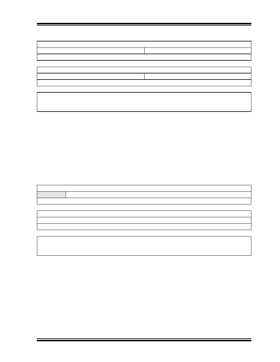
©
2006 Microchip Technology Inc.
Advance Information
DS70178A-page 195
dsPIC30F1010/202X
REGISTER 18-4:
LFSR: LINEAR FEEDBACK SHIFT REGISTER
REGISTER 18-3:
OSCTUN2: OSCILLATOR TUNING REGISTER
R/W-0
R/W-0
R/W-0
R/W-0
R/W-0
R/W-0
R/W-0
R/W-0
TSEQ7<3:0>
TSEQ6<3:0>
bit 15
bit 8
R/W-0
R/W-0
R/W-0
R/W-0
R/W-0
R/W-0
R/W-0
R/W-0
TSEQ5<3:0>
TSEQ4<3:0>
bit 7
bit 0
Legend:
R = Readable bit
W = Writable bit
U = Unimplemented bit, read as `0'
-n = Value at POR
`1' = Bit is set
`0' = Bit is cleared
x = Bit is unknown
bit 15-12
TSEQ7<3:0>: Tune Sequence value #7 bits
When PWM ROLL<2:0> =
111
, this field is used to tune the FRC instead of TUN<3:0>
bit 11-8
TSEQ6<3:0>: Tune Sequence value #6 bits
When PWM ROLL<2:0> =
110
, this field is used to tune the FRC instead of TUN<3:0>
bit 7-4
TSEQ5<3:0>: Tune Sequence value #5 bits
When PWM ROLL<2:0> =
101
, this field is used to tune the FRC instead of TUN<3:0>
bit 3-0
TSEQ4<3:0>: Tune Sequence value #4 bits
When PWM ROLL<2:0> =
100
, this field is used to tune the FRC instead of TUN<3:0>
U-0
R/W-0
R/W-0
R/W-0
R/W-0
R/W-0
R/W-0
R/W-0
--
LFSR<14:8>
bit 15
bit 8
R/W-0
R/W-0
R/W-0
R/W-0
R/W-0
R/W-0
R/W-0
R/W-0
LFSR<7:0>
bit 7
bit 0
Legend:
R = Readable bit
W = Writable bit
U = Unimplemented bit, read as `0'
-n = Value at POR
`1' = Bit is set
`0' = Bit is cleared
x = Bit is unknown
bit 15
Unimplemented: Read as `
0
'
When PS PWM ROLL<2:0> =
111
, this field is used to tune the FRC instead of TUN<3:0>
bit 14-8
LFSR <14:8>: Most Significant 7 bits of the pseudo random FRC trim value bits
bit 7-0
LFSR <7:0>: Least Significant 8 bits of the pseudo random FRC trim value bits

dsPIC30F1010/202X
DS70178A-page 196
Advance Information
©
2006 Microchip Technology Inc.
18.2.1
PROTECTION AGAINST
ACCIDENTAL WRITES TO OSCCON
REGISTER
Because the OSCCON register allows clock switching
and clock scaling, a write to OSCCON is intentionally
made difficult.
To write to OSCCON low byte, this exact sequence
must be executed without any other instructions in
between:
∑ Byte Write "46h" to OSCCON low
∑ Byte Write "57h" to OSCCON low
∑ Byte Write is allowed for one instruction cycle.
mov.b W0,OSCCON
To write to OSCCON high byte, this exact sequence
must be executed without any other instructions in
between:
∑ Byte Write "78h" to OSCCON high
∑ Byte Write "9Ah" to OSCCON high
∑ Byte Write is allowed for one instruction cycle.
mov.b W0,OSCCON + 1

©
2006 Microchip Technology Inc.
Advance Information
DS70178A-page 197
dsPIC30F1010/202X
REGISTER 18-5:
FOSCSEL: OSCILLATOR SELECTION CONFIGURATION BITS
U
U
U
U
U
U
U
U
--
--
--
--
--
--
--
--
bit 23
bit 16
U
U
U
U
U
U
U
U
--
--
--
--
--
--
--
--
bit 15
bit 8
U
U
U
U
U
U
R/P
R/P
--
--
--
--
--
--
FNOSC1
FNOSC0
bit 7
bit 0
Legend:
R = Readable bit
W = Writable bit
U = Unimplemented bit, read as `0'
-n = Value at POR
`1' = Bit is set
`0' = Bit is cleared
x = Bit is unknown
bit 23-2
Unimplemented: Read as `
0
'
bit 1-0
FNOSC<1:0>: Initial Oscillator Group Selection on POR bits
00
= Fast RC Oscillator (FRC)
01
= Fast RC Oscillator (FRC) divided by N, with PLL module.
10
= Primary Oscillator (HS,EC).
11
= Primary Oscillator (HS,EC) with PLL module.
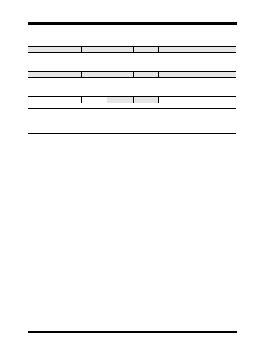
dsPIC30F1010/202X
DS70178A-page 198
Advance Information
©
2006 Microchip Technology Inc.
scillator Operating Modes
REGISTER 18-6:
FOSC: OSCILLATOR SELECTION CONFIGURATION BITS
U
U
U
U
U
U
U
U
--
--
--
--
--
--
--
--
bit 23
bit 16
U
U
U
U
U
U
U
U
--
--
--
--
--
--
--
--
bit 15
bit 8
R/P
R/P
R/P
U
U
R/P
R/P
R/P
FCKSM<1:0>
FRANGE
--
--
OSCIOFNC
POSCMD<1:0>
bit 7
bit 0
Legend:
R = Readable bit
W = Writable bit
U = Unimplemented bit, read as `0'
-n = Value at POR
`1' = Bit is set
`0' = Bit is cleared
x = Bit is unknown
bit 23-8
Unimplemented: Read as `
0
'
bit 7-6
FCKSM<1:0>: Clock Switching and Monitor Selection Configuration bits
1x
= Clock switching is disabled, fail-safe clock monitor is disabled.
01
= Clock switching is enabled, fail-safe clock monitor is disabled.
00
= Clock switching is enabled, fail-safe clock monitor is enabled
bit 5
FRANGE: Frequency Range Select for FRC and PLL bit
Acts like a "Gear Shift" feature that enables the dsPIC DSC device to operate at reduced MIPS at a
reduced supply voltage (3.3V)
0
= "Low Range" (FRC operates at a nominal 9.7 MHz, PLL VCO at a nominal 301 MHz (320 max))
1
= "High Range" (FRC operates at a nominal 14.55 MHz, PLL VCO at a nominal 451 MHz. (480 max))
bit 4-3
Unimplemented: Read as `
0
'
bit 3
OSCIOFNC: OSC2 PIn I/O Enable bit
1
= CLKO output signal active on the OSCO pin.
0
= CLKO output disabled
bit 1-0
POSCMD<1:0>: Primary Oscillator Mode
11
= Primary Oscillator Disabled
10
= HS oscillator mode selected.
01
= Reserved
00
= External clock mode selected.

©
2006 Microchip Technology Inc.
Advance Information
DS70178A-page 199
dsPIC30F1010/202X
FIGURE 18-1:
OSCILLATOR SYSTEM BLOCK DIAGRAM
Primary
OSC1
OSC2
Oscillator
Clock
and Control
Block
Switching
x32
PLL
Primary
Oscillator
Stability Detector
Programmable
Clock Divider
Oscillator
Start-up
Timer
Fail-Safe Clock
Monitor (FSCM)
Internal Fast RC
Oscillator (FRC)
Internal
Low-Power RC
Oscillator (LPRC)
PWRSAV
Instruction
Wake-up Request
Oscillator Configuration Bits
System
Clock
Oscillator Trap
POR Done
Primary Osc
F
PLL
POST<1:0>
2
FCKSM<1:0>
2
PLL
Lock
COSC<1:0>
NOSC<1:0>
OSWEN
CF
TUN<3:0>
4
FPWM
Clock Dither
Circuit
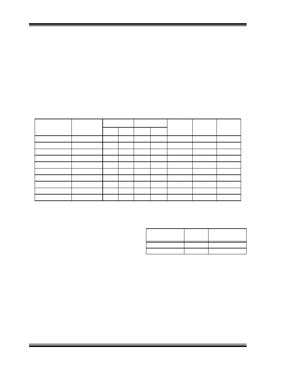
dsPIC30F1010/202X
DS70178A-page 200
Advance Information
©
2006 Microchip Technology Inc.
18.3
Oscillator Configurations
18.3.1
INITIAL CLOCK SOURCE
SELECTION
While coming out of a Power-on Reset, the device
selects its clock source based on:
a)
FNOSC<1:0> Configuration bits that select one
of three oscillator groups (HS, EC or FRC)
b)
POSCMD1<1:0> Configuration bits that select
the Primary Oscillator Mode
c)
OSCIOFNC selects if the OSC2 pin is an I/O or
clock output
The selection is as shown in Table 18-1.
TABLE 18-1:
CONFIGURATION BIT VALUES FOR CLOCK SELECTION
18.3.2
OSCILLATOR START-UP TIMER
(OST)
In order to ensure that a crystal oscillator (or ceramic
resonator) has started and stabilized, an Oscillator
Start-up Timer is included. It is a simple 10-bit counter
that counts 1024 T
OSC
cycles before releasing the
oscillator clock to the rest of the system. The time-out
period is designated as T
OST
. The T
OST
time is involved
every time the oscillator has to restart (i.e., on POR and
wake-up from Sleep). The Oscillator Start-up Timer is
applied to the HS Oscillator mode (upon wake-up from
Sleep and POR) for the primary oscillator.
18.3.3
PHASE LOCKED LOOP (PLL)
The PLL multiplies the clock, which is generated by the
primary oscillator. The PLL is selectable to have a gain
of x32 only. Input and output frequency ranges are
summarized in Table 18-2.
TABLE 18-2:
PLL FREQUENCY RANGE
The PLL features a lock output, which is asserted when
the PLL enters a phase locked state. Should the loop
fall out of lock (e.g., due to noise), the lock signal will be
rescinded. The state of this signal is reflected in the
read-only LOCK bit in the OSCCON register.
Oscillator
Mode
Oscillator
Source
FNOSC<1:0>
POSCMD<1:0>
OSCIOFNC
OSC2
Function
OSC1
Function
Bit 1
Bit 0
Bit 1
Bit 0
HS w/PLL 32x
PLL
1
1
1
0
N/A
CLKOUT
(1)
CLKI
FRC w/PLL 32x
PLL
0
1
1
1
1
CLKOUT
I/O
FRC w/PLL 32x
PLL
0
1
1
1
0
I/O
I/O
EC w/PLL 32x
PLL
1
1
0
0
1
CLKOUT
CLKI
EC w/PLL 32x
PLL
1
1
0
0
0
I/O
CLKI
EC
(2)
External
1
0
0
0
1
CLKOUT
CLKI
EC
(2)
External
1
0
0
0
0
I/O
CLKI
HS
(2)
External
1
0
1
0
N/A
CLKOUT
(1)
CLKI
FRC
(2)
Internal RC
0
0
1
1
0
I/O
I/O
FRC
(2)
Internal RC
0
0
1
1
1
CLKOUT
I/O
Note 1:
CLKOUT is not recommended to drive external circuits.
2:
This mode is not recommended for some applications; disabling 32x PLL will not allow operation of
high-speed ADC and PWM.
F
IN
PLL
Multiplier
F
OUT
9.7 MHz
x32
310 MHz
14.55 MHz
x32
466 MHz

©
2006 Microchip Technology Inc.
Advance Information
DS70178A-page 201
dsPIC30F1010/202X
18.4
PRIMARY OSCILLATOR ON OSC1/
OSC2 PINS:
The primary oscillator uses is shown in Figure 18-2.
FIGURE 18-2:
PRIMARY OSCILLATOR
18.5
EXTERNAL CLOCK INPUT
Two of the primary Oscillator modes use an external
clock. These modes are EC and EC with IO.
In the EC mode (Figure 18-3), the OSC1 pin can be
driven by CMOS drivers. In this mode, the OSC1 pin is
high-impedance and the OSC2 pin is the clock output
(F
OSC
/2). This output clock is useful for testing or
synchronization purposes.
In the EC with IO mode (Figure 18-4), the OSC1 pin
can be driven by CMOS drivers. In this mode, the
OSC1 pin is high-impedance and the OSC2 pin
becomes a general purpose I/O pin. The feedback
device between OSC1 and OSC2 is turned off to save
current.
FIGURE 18-3:
EXTERNAL CLOCK INPUT OPERATION (EC OSCILLATOR CONFIGURATION)
FIGURE 18-4:
EXTERNAL CLOCK INPUT OPERATION (ECIO OSCILLATOR CONFIGURATION)
C1
C2
XTAL
OSC2/CLKO
Rs
(1)
OSC1/CLKI
R
F
(2)
Note 1: A series resistor, Rs, may be required for AT strip cut crystals.
2: The feedback resistor, R
F
, is typically in the range of 2 to 10 M
.
To CLKGEN
CLKO/RC15
OSC1
OSC2
F
OSC
/2
dsPIC30F
Clock from Ext System
OSC1
I/O (OSC2)
I/O
dsPIC30F
Clock from Ext System

dsPIC30F1010/202X
DS70178A-page 202
Advance Information
©
2006 Microchip Technology Inc.
18.6
INTERNAL FAST RC OSCILLATOR
(FRC)
FRC is a fast, precise frequency internal RC oscillator.
The FRC oscillator is designed to run at a frequency of
9.7/14.55 MHz (±1% accuracy). The FRC oscillator
option is intended to be accurate enough to provide
the clock frequency necessary to maintain baud rate
tolerance for serial data transmissions. The user has
the ability to tune the FRC frequency by +-3%.
The FRC oscillator is powered:
a)
Any time the EC or HS Oscillator modes are
NOT selected.
b)
When the fail-safe clock monitor is enabled and
a clock fail is detected, forcing a switch to FRC.
18.6.1
FREQUENCY RANGE SELECTION
The FRC module has a "Gear Shift" control signal that
selects "Low Range" (9.7 MHz) or "High Range"
(14.55 MHz) frequency of operation. This feature
enables a dsPIC DSC device to operate at 3.3V/5.0V
at 20/30 MIPS and remain with system specifications.
18.6.2
NOMINAL FREQUENCY VALUES
The FRC module is calibrated to a nominal 9.7 MHz in
"Low Range" and 14.55 MHz in "High Range" This fea-
ture enables a user to "TUNE" the dsPIC DSC device
frequency of operation by +-3% and still remain within
system specifications.
18.6.3
FRC FREQUENCY USER TUNING
The FRC is calibrated at the factory to give a nominal
9.7/14.55 MHz. The TUN<3:0> field in the OSCTUN
register is available to the user for trimming the FRC
oscillator frequency in applications.
The 4-bit tuning control signals are supplied by the
OSCTUN or the OSCTUN2 registers depending on
the TSEQEN bit in the OSCCON register.
The tuning range of the 15 MHz oscillator is
±0.45 MHz (±3%) nominal.
The base frequency can be tuned in the user's appli-
cation. This frequency tuning capability allows the user
to deviate from the factory calibrated frequency. The
user can tune the frequency by writing to the OSCTUN
register TUN<3:0> bits.
18.6.4
CLOCK DITHERING LOGIC
In power conversion applications, the primary electri-
cal noise emission that the designers want to reduce is
caused by the power transistors switching at the PWM
frequency. By changing the system clock frequency of
the SMPS dsPIC DSC, the resultant PWM frequency
will change and the peak EMI will be reduced at the
noise is spread over a wider frequency range.
Typically, the range of frequency variation is few
percent. The dsPIC30F1010/202X can provide two
ways to vary system clock frequency on a PWM cycle
basis. These are Frequency Sequencing mode and
Pseudo Random Clock Dithering mode. Table 18-5
shows the implementation details of both these
methods.
18.6.5
FREQUENCY SEQUENCING MODE
The Frequency Sequencing mode enables the PWM
module to select a sequence of eight different FRC
TUN values to vary the system frequency with each
rollover of the primary PWM time base. The OSCTUN
and the OSCTUN2 registers allow the user to specify
eight sequential tune values if the TSEQEN bit is set in
the OSCCON register. If the TSEQEN bit is zero, then
only the TUN bits affect the FRC frequency.
A 4-bit wide multiplexer with eight sets of inputs
selects the tuning value from the TUN and the TSEQx
bit fields. The multiplexer is controlled by the
ROLL<5:3> counter in the PWM module. The
ROLL<5:3> counter increments every time the primary
time base rolls over after reaching the period value.
18.6.6
PSEUDO RANDOM CLOCK
DITHERING MODE
The Pseudo Random Clock Dither (PRCD) logic is
implemented with a 15-bit LFSR (Linear Feedback
Shift Register), which is a shift register with a few
exclusive OR gates. The lower four bits of the LFSR
provides the FRC TUNE bits. The PRCD feature is
enabled by setting the PRCDEN bit in the OSCCON
register. The LSFR is "clocked" (enabled to clock)
once every time the ROLL<3> bit changes state,
which occurs once every 8 PWM cycles.
18.6.7
FAIL-SAFE CLOCK MONITOR
The Fail-Safe Clock Monitor (FSCM) allows the device
to continue to operate even in the event of an oscillator
failure. The FSCM function is enabled by appropriately
programming the FCKSM Configuration bits (Clock
Switch and Monitor Selection bits) in the FOSC
Configuration register.
In the event of an oscillator failure, the FSCM will
generate a clock failure trap event and will switch the
system clock over to the FRC oscillator. The user will
then have the option to either attempt to restart the
oscillator or execute a controlled shutdown. The user
may decide to treat the trap as a warm Reset by sim-
ply loading the Reset address into the oscillator fail
trap vector. In this event, the CF (Clock Fail) status bit
(OSCCON<3>) is also set whenever a clock failure is
recognized.
In the event of a clock failure, the WDT is unaffected
and continues to run on the LPRC clock.
If the oscillator has a very slow start-up time coming
out of POR or Sleep, it is possible that the PWRT timer
will expire before the oscillator has started. In such
cases, the FSCM will be activated and the FSCM will

©
2006 Microchip Technology Inc.
Advance Information
DS70178A-page 203
dsPIC30F1010/202X
initiate a clock failure trap, and the COSC<2:0> bits
are loaded with FRC oscillator selection. This will
effectively shut off the original oscillator that was trying
to start.
The user may detect this situation and restart the
oscillator in the clock fail trap, ISR.
Upon a clock failure detection, the FSCM module will
initiate a clock switch to the FRC oscillator as follows:
1.
The COSC bits (OSCCON<14:12>) are loaded
with the FRC oscillator selection value
2.
CF bit is set (OSCCON<3>)
3.
OSWEN control bit (OSCCON<0>) is cleared
For the purpose of clock switching, the clock sources
are sectioned into two groups:
1.
Primary
2.
Internal FRC
The user can switch between these functional groups,
but cannot switch between options within a group. If the
primary group is selected, then the choice within the
group is always determined by the FNOSC<1:0>
Configuration bits.
The OSCCON register holds the control and status bits
related to clock switching. If Configuration bits
FCKSM<1:0> =
1x
, then the clock switching and Fail-
Safe Clock Monitor functions are disabled. This is the
default Configuration bit setting.
If clock switching is disabled, then the FNOSC<1:0>
and POSCMD<1:0> bits directly control the oscillator
selection and the COSC<2:0> bits do not control the
clock selection. However, these bits will reflect the
clock source selection.
18.7
Reset
The dsPIC30F1010/202X differentiates between
various kinds of Reset:
a)
Power-on Reset (POR)
b)
MCLR Reset during normal operation
c)
MCLR Reset during Sleep
d)
Watchdog Timer (WDT) Reset (during normal
operation)
e)
RESET
Instruction
f)
Reset cause by trap lock-up (TRAPR)
g)
Reset caused by illegal opcode, or by using an
uninitialized W register as an Address Pointer
(IOPUWR)
Different registers are affected in different ways by var-
ious Reset conditions. Most registers are not affected
by a WDT wake-up, since this is viewed as the resump-
tion of normal operation. Status bits from the RCON
register are set or cleared differently in different Reset
situations, as indicated in Table 18-3. These bits are
used in software to determine the nature of the Reset.
A block diagram of the on-chip Reset circuit is shown in
Figure 18-6.
A MCLR noise filter is provided in the MCLR Reset
path. The filter detects and ignores small pulses.
Internally generated Resets do not drive MCLR pin low.
Note:
The application should not attempt to
switch to a clock frequency lower than 100
KHz when the Fail-Safe Clock Monitor is
enabled. If clock switching is performed,
the device may generate an oscillator fail
trap and switch to the Fast RC oscillator.
dsPIC30F1010/202X
DS70178A-page 204
Advance Information
©
2006 Microchip Technology Inc.
FIGURE 18-5:
FRC TUNE DITHER LOGIC BLOCK DIAGRAM
FIGURE 18-6:
RESET SYSTEM BLOCK DIAGRAM
D Q
CLK
3
TUNE BIts to FRC
All Zero Detect
TSEQEN in OSCCON
15
ROLL<3>
0
1
TSEQ7
4
D
Q0
CLK Q
D
Q1
CLK Q
D
Q2
CLK Q
D
Q3
CLK Q
D
Q4
CLK Q
D
Q5
CLK Q
D
Q6
CLK Q
D
Q7
CLK Q
D
Q8
CLK Q
D
Q9
CLK Q
D Q10
CLK Q
D Q11
CLK Q
D Q12
CLK Q
D Q13
CLK Q
D Q14
CLK Q
LFSR
PWM PS
TSEQ6 TSEQ5 TSEQ4
0
15
OSCTUN2
TSEQ3 TSEQ2 TSEQ1 TUN
0
15
OSCTUN
3
4
3
12
12 11
7
11
0
1
2
3
4
5
6
8
4
MU
X
ROLL Counter
ROLL<5:3> ROLL<2:0>
MU
X
4
Shift Enable for LFSR
4
PRCDEN in OSCCON
S
R
Q
MCLR
V
DD
V
DD
Rise
Detect
POR
SYSRST
Sleep or Idle
WDT
Module
Digital
Glitch Filter
Trap Conflict
Illegal Opcode/
Uninitialized W Register
RESET
Instruction

©
2006 Microchip Technology Inc.
Advance Information
DS70178A-page 205
dsPIC30F1010/202X
18.7.1
POR: POWER-ON RESET
A power-on event will generate an internal POR pulse
when a V
DD
rise is detected. The Reset pulse will occur
at the POR circuit threshold voltage (V
POR
), which is
nominally 1.85V. The device supply voltage character-
istics must meet specified starting voltage and rise rate
requirements. The POR pulse will reset a POR timer
and place the device in the Reset state. The POR also
selects the device clock source identified by the
oscillator configuration fuses.
The POR circuit inserts a small delay, T
POR
, which is
nominally 10
s and ensures that the device bias
circuits are stable. Furthermore, a user selected power-
up time-out (T
PWRT
) is applied. The T
PWRT
parameter
is based on Configuration bits and can be 0 ms (no
delay), 4 ms, 16 ms or 64 ms. The total delay is at
device power-up T
POR
+ T
PWRT
. When these delays
have expired, SYSRST will be negated on the next
leading edge of the Q1 clock, and the PC will jump to
the Reset vector.
The timing for the SYSRST signal is shown in
Figure 18-7 through Figure 18-9.
FIGURE 18-7:
TIME-OUT SEQUENCE ON POWER-UP (MCLR TIED TO V
DD
)
FIGURE 18-8:
TIME-OUT SEQUENCE ON POWER-UP (MCLR NOT TIED TO V
DD
): CASE 1
T
PWRT
T
OST
V
DD
Internal POR
PWRT Time-out
OST Time-out
Internal Reset
MCLR
T
PWRT
T
OST
V
DD
Internal POR
PWRT Time-out
OST Time-out
Internal Reset
MCLR

dsPIC30F1010/202X
DS70178A-page 206
Advance Information
©
2006 Microchip Technology Inc.
FIGURE 18-9:
TIME-OUT SEQUENCE ON POWER-UP (MCLR NOT TIED TO V
DD
): CASE 2
18.7.1.1
POR with Long Crystal Start-up Time
(with FSCM Enabled)
The oscillator start-up circuitry is not linked to the POR
circuitry. Some crystal circuits (especially low
frequency crystals) will have a relatively long start-up
time. Therefore, one or more of the following conditions
is possible after the POR timer and the PWRT have
expired:
∑ The oscillator circuit has not begun to oscillate.
∑ The Oscillator Start-up Timer has NOT expired (if
a crystal oscillator is used).
∑ The PLL has not achieved a LOCK (if PLL is
used).
If the FSCM is enabled and one of the above conditions
is true, then a clock failure trap will occur. The device
will automatically switch to the FRC oscillator and the
user can switch to the desired crystal oscillator in the
trap, ISR.
18.7.1.2
Operating without FSCM and PWRT
If the FSCM is disabled and the Power-up Timer
(PWRT) is also disabled, then the device will exit rap-
idly from Reset on power-up. If the clock source is FRC
or EC, it will be active immediately.
If the FSCM is disabled and the system clock has not
started, the device will be in a frozen state at the Reset
vector until the system clock starts. From the user's
perspective, the device will appear to be in Reset until
a system clock is available.
FIGURE 18-10:
EXTERNAL POWER-ON
RESET CIRCUIT (FOR
SLOW V
DD
POWER-UP)
V
DD
MCLR
Internal POR
PWRT Time-out
OST Time-out
Internal Reset
T
PWRT
T
OST
Note:
Dedicated supervisory devices, such as
the MCP1XX and MCP8XX, may also be
used as an external Power-on Reset
circuit.
Note 1: External Power-on Reset circuit is
required only if the V
DD
power-up slope
is too slow. The diode D helps discharge
the capacitor quickly when V
DD
powers
down.
2: R should be suitably chosen so as to
make sure that the voltage drop across
R does not violate the device's electrical
specification.
3: R1 should be suitably chosen so as to
limit any current flowing into MCLR from
external capacitor C, in the event of
MCLR/V
PP
pin breakdown due to Elec-
trostatic Discharge (ESD) or Electrical
Overstress (EOS).
C
R1
R
D
V
DD
dsPIC30F
MCLR
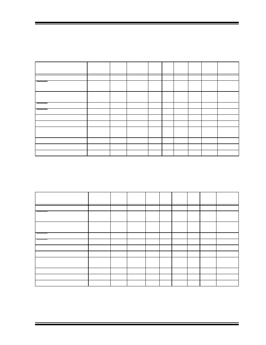
©
2006 Microchip Technology Inc.
Advance Information
DS70178A-page 207
dsPIC30F1010/202X
Table 18-3 shows the Reset conditions for the RCON
register. Since the control bits within the RCON register
are R/W, the information in the table implies that all the
bits are negated prior to the action specified in the
condition column.
TABLE 18-3:
INITIALIZATION CONDITION FOR RCON REGISTER CASE 1
Table 18-4 shows a second example of the bit
conditions for the RCON register. In this case, it is not
assumed the user has set/cleared specific bits prior to
action specified in the condition column.
TABLE 18-4:
INITIALIZATION CONDITION FOR RCON REGISTER CASE 2
Condition
Program
Counter
TRAPR
IOPUWR
EXTR SWR WDTO IDLE
SLEEP
POR
Power-on Reset
0x000000
0
0
0
0
0
0
0
1
MCLR Reset during normal
operation
0x000000
0
0
1
0
0
0
0
0
Software Reset during
normal operation
0x000000
0
0
0
1
0
0
0
0
MCLR Reset during Sleep
0x000000
0
0
1
0
0
0
1
0
MCLR Reset during Idle
0x000000
0
0
1
0
0
1
0
0
WDT Time-out Reset
0x000000
0
0
0
0
1
0
0
0
WDT Wake-up
PC + 2
0
0
0
0
1
0
1
0
Interrupt Wake-up from
Sleep
PC + 2
(1)
0
0
0
0
0
0
1
0
Clock Failure Trap
0x000004
0
0
0
0
0
0
0
0
Trap Reset
0x000000
1
0
0
0
0
0
0
0
Illegal Operation Trap
0x000000
0
1
0
0
0
0
0
0
Note 1:
When the wake-up is due to an enabled interrupt, the PC is loaded with the corresponding interrupt vector.
Condition
Program
Counter
TRAPR IOPUWR EXTR SWR WDTO
IDLE
SLEEP
POR
Power-on Reset
0x000000
0
0
0
0
0
0
0
1
MCLR Reset during normal
operation
0x000000
u
u
1
0
0
0
0
u
Software Reset during
normal operation
0x000000
u
u
0
1
0
0
0
u
MCLR Reset during Sleep
0x000000
u
u
1
u
0
0
1
u
MCLR Reset during Idle
0x000000
u
u
1
u
0
1
0
u
WDT Time-out Reset
0x000000
u
u
0
0
1
0
0
u
WDT Wake-up
PC + 2
u
u
u
u
1
u
1
u
Interrupt Wake-up from
Sleep
PC + 2
(1)
u
u
u
u
u
u
1
u
Clock Failure Trap
0x000004
u
u
u
u
u
u
u
u
Trap Reset
0x000000
1
u
u
u
u
u
u
u
Illegal Operation Reset
0x000000
u
1
u
u
u
u
u
u
Legend:
u
= unchanged
Note 1:
When the wake-up is due to an enabled interrupt, the PC is loaded with the corresponding interrupt vector.

dsPIC30F1010/202X
DS70178A-page 208
Advance Information
©
2006 Microchip Technology Inc.
18.8
Watchdog Timer (WDT)
18.8.1
WATCHDOG TIMER OPERATION
The primary function of the Watchdog Timer (WDT) is
to reset the processor in the event of a software
malfunction. The WDT is a free-running timer, which
runs off an on-chip RC oscillator, requiring no external
component. Therefore, the WDT timer will continue to
operate even if the main processor clock (e.g., the
crystal oscillator) fails.
18.8.2
ENABLING AND DISABLING THE
WDT
The Watchdog Timer can be "enabled" or "disabled"
only through a Configuration bit (FWDTEN) in the
Configuration register FWDT.
Setting FWDTEN =
1
enables the Watchdog Timer.
The enabling is done when programming the device.
By default, after chip-erase, FWDTEN bit =
1
. Any
device programmer capable of programming
dsPIC30F devices allows programming of this and
other Configuration bits.
If enabled, the WDT will increment until it overflows or
"times out". A WDT time-out will force a device Reset
(except during Sleep). To prevent a WDT time-out, the
user must clear the Watchdog Timer using a
CLRWDT
instruction.
If a WDT times out during Sleep, the device will wake-
up. The WDTO bit in the RCON register will be cleared
to indicate a wake-up resulting from a WDT time-out.
Setting FWDTEN =
0
allows user software to enable/
disable the Watchdog Timer via the SWDTEN
(RCON<5>) control bit.
18.9
Power-Saving Modes
There are two power-saving states that can be entered
through the execution of a special instruction,
PWRSAV
.
These are: Sleep and Idle.
The format of the
PWRSAV
instruction is as follows:
PWRSAV <parameter>
, where `
parameter
' defines
Idle or Sleep mode.
18.9.1
SLEEP MODE
In Sleep mode, the clock to the CPU and peripherals is
shutdown. If an on-chip oscillator is being used, it is
shutdown.
The Fail-Safe Clock Monitor is not functional during
Sleep, since there is no clock to monitor. However,
LPRC clock remains active if WDT is operational during
Sleep.
The processor wakes up from Sleep if at least one of
the following conditions has occurred:
∑ any interrupt that is individually enabled and
meets the required priority level
∑ any Reset (POR and MCLR)
∑ WDT time-out
On waking up from Sleep mode, the processor will
restart the same clock that was active prior to entry
into Sleep mode. When clock switching is enabled,
bits COSC<2:0> will determine the oscillator source
that will be used on wake-up. If clock switch is
disabled, then there is only one system clock.
If the clock source is an oscillator, the clock to the
device is held off until OST times out (indicating a sta-
ble oscillator). If PLL is used, the system clock is held
off until LOCK =
1
(indicating that the PLL is stable).
Either way, T
POR
, T
LOCK
and T
PWRT
delays are applied.
If EC, FRC, oscillators are used, then a delay of T
POR
(~10
s) is applied. This is the smallest delay possible
on wake-up from Sleep.
Moreover, if LP oscillator was active during Sleep, and
LP is the oscillator used on wake-up, then the start-up
delay will be equal to T
POR
.
PWRT delay and OST
timer delay are not applied. In order to have the small-
est possible start-up delay when waking up from Sleep,
one of these faster wake-up options should be selected
before entering Sleep.
Any interrupt that is individually enabled (using the
corresponding IE bit) and meets the prevailing priority
level will be able to wake-up the processor. The proces-
sor will process the interrupt and branch to the ISR. The
Sleep status bit in the RCON register is set upon
wake-up.
All Resets will wake-up the processor from Sleep
mode. Any Reset, other than POR, will set the Sleep
status bit. In a POR, the Sleep bit is cleared.
If Watchdog Timer is enabled, then the processor will
wake-up from Sleep mode upon WDT time-out. The
Sleep and WDTO status bits are both set.
Note:
If a POR occurred, the selection of the
oscillator is based on the FGS<2:0> and
FPG<1:0> Configuration bits.
Note:
In spite of various delays applied (T
POR
,
T
LOCK
and T
PWRT
), the crystal oscillator
(and PLL) may not be active at the end of
the time-out (e.g., for low frequency crys-
tals). In such cases, if FSCM is enabled, the
device will detect this as a clock failure and
process the clock failure trap, the FRC
oscillator will be enabled, and the user will
have to re-enable the crystal oscillator. If
FSCM is not enabled, then the device will
simply suspend execution of code until the
clock is stable, and will remain in Sleep until
the oscillator clock has started.

©
2006 Microchip Technology Inc.
Advance Information
DS70178A-page 209
dsPIC30F1010/202X
18.9.2
IDLE MODE
In Idle mode, the clock to the CPU is shutdown while
peripherals keep running. Unlike Sleep mode, the clock
source remains active.
Several peripherals have a control bit in each module
that allows them to operate during Idle.
LPRC fail-safe clock remains active if clock failure
detect is enabled.
The processor wakes up from Idle if at least one of the
following conditions is true:
∑ on any interrupt that is individually enabled (IE bit
is `
1
') and meets the required priority level
∑ on any Reset (POR, MCLR)
∑ on WDT time-out
Upon wake-up from Idle mode, the clock is re-applied
to the CPU and instruction execution begins immedi-
ately, starting with the instruction following the
PWRSAV
instruction.
Any interrupt that is individually enabled (using IE bit)
and meets the prevailing priority level will be able to
wake-up the processor. The processor will process the
interrupt and branch to the ISR. The Idle status bit in
RCON register is set upon wake-up.
Any Reset, other than POR, will set the Idle status bit.
On a POR, the Idle bit is cleared.
If Watchdog Timer is enabled, then the processor will
wake-up from Idle mode upon WDT time-out. The Idle
and WDTO status bits are both set.
Unlike wake-up from Sleep, there are no time delays
involved in wake-up from Idle.
18.10 Device Configuration Registers
The Configuration bits in each device Configuration
register specify some of the device modes and are
programmed by a device programmer, or by using the
In-Circuit Serial Programming (ICSP) feature of the
device. Each device Configuration register is a 24-bit
register, but only the lower 16 bits of each register are
used to hold configuration data. There are four
Configuration registers available to the user:
1.
FOSC (0xF80000): Oscillator Configuration
Register
2.
FWDT (0xF80002): Watchdog Timer
Configuration Register
3.
FGS (0xF8000A): General Code Segment
Configuration Register
The placement of the Configuration bits is automati-
cally handled when you select the device in your device
programmer. The desired state of the Configuration bits
may be specified in the source code (dependent on the
language tool used), or through the programming
interface. After the device has been programmed, the
application software may read the Configuration bit
values through the table read instructions. For addi-
tional information, please refer to the programming
specifications of the device.
Note:
If the code protection configuration fuse
bits (FGS<GCP> and FGS<GWRP>)
have been programmed, an erase of the
entire code-protected device is only
possible at voltages V
DD
4.5V.

dsPIC30F1010/202X
DS70178A-page 210
Advance Information
©
2006 Microchip Technology Inc.
18.11 In-Circuit Debugger
When MPLAB
Æ
ICD 2 is selected as a debugger, the
in-circuit debugging functionality is enabled. This func-
tion allows simple debugging functions when used with
MPLAB IDE. When the device has this feature enabled,
some of the resources are not available for general
use. These resources include the first 80 bytes of data
RAM and two I/O pins.
One of four pairs of Debug I/O pins may be selected by
the user using configuration options in MPLAB IDE.
These pin pairs are named EMUD/EMUC, EMUD1/
EMUC1, EMUD2/EMUC2 and EMUD3/EMUC3.
In each case, the selected EMUD pin is the Emulation/
Debug Data line, and the EMUC pin is the Emulation/
Debug Clock line. These pins will interface to the
MPLAB ICD 2 module available from Microchip. The
selected pair of Debug I/O pins is used by
MPLAB ICD 2 to send commands and receive
responses, as well as to send and receive data. To use
the in-circuit debugging function of the device, the
design must implement ICSP connections to MCLR,
V
DD
, V
SS
, PGC, PGD and the selected
EMUDx/EMUCx pin pair.
This gives rise to two possibilities:
1.
If EMUD/EMUC is selected as the debug I/O pin
pair, then only a 5-pin interface is required, as
the EMUD and EMUC pin functions are multi-
plexed with the PGD and PGC pin functions in
all dsPIC30F devices.
2.
If EMUD1/EMUC1, EMUD2/EMUC2 or EMUD3/
EMUC3 is selected as the debug I/O pin pair,
then a 7-pin interface is required, as the
EMUDx/EMUCx pin functions (x = 1, 2 or 3) are
not multiplexed with the PGD and PGC pin
functions.

©
2006 Microchip Technology Inc.
Advance Information
DS70178A-page 211
dsPIC30F1010/202X
T
A
BLE
1
8
-5:
S
Y
S
TE
M I
N
TE
GRATION R
E
GIS
T
E
R
M
A
P
F
O
R
d
s
P
I
C
30F20
2X
T
A
BLE
1
8
-6:
D
E
V
ICE
CONFIGURATION
RE
GIS
T
E
R
M
A
P
SF
R
Na
m
e
Ad
d
r
.
B
it 1
5
Bit 1
4
Bit
13
Bit
12
Bi
t 1
1
Bit 1
0
Bit
9
B
it 8
B
it
7
B
it 6
B
it
5
B
it 4
B
i
t
3
B
it
2
B
it 1
B
i
t
0
R
e
s
e
t
S
t
at
e
RC
O
N
0
7
4
0
TRAPR
I
O
PUWR
--
--
--
--
--
--
EXTR
S
WR
SWDTE
N
WDT
O
SL
EEP
I
D
L
E
--
P
OR
D
epe
nd
s on
type
of
R
e
se
t.
O
S
CCON
0
7
4
2
--C
O
S
C
<
2
:
0
>
--
N
OS
C
<
2:
0>
CL
KL
O
C
K
--
L
O
C
K
P
R
CDE
N
C
F
TS
E
Q
E
N
--O
S
W
E
N
D
e
pen
ds
on C
o
nf
i
g
urat
i
o
n
bi
t
s
.
O
S
CT
UN
07
48
T
S
E
Q
3<
3
:
0>
T
S
E
Q
2<
3:
0>
T
S
E
Q
1<
3
:
0>
T
U
N
<
3:0
>
0000
0000 0000 0000
O
S
C
T
U
N
2
074
A
T
S
E
Q
7<
3
:
0>
T
S
E
Q
6<
3:
0>
T
S
E
Q
5<
3
:
0>
TSEQ
4
<
3:0
>
0000
0000 0000 0000
L
F
S
R
07
4C
--
LF
S
R
<
14:0
>
0000
0000 0000 0000
P
M
D
1
07
70
--
--
T
3MD
T
2M
D
T
1
M
D
--P
W
M
M
D
--I
2
C
M
D
--U
1
M
D
--
SPI
1
M
D
--
--
A
DCM
D
0000
0000 0000 0000
P
M
D
2
07
72
--
--
--
--
--
--
--I
C
1
M
D
--
--
--
--
--
--O
C
2
M
D
O
C
1
M
D
0000
0000 0000 0000
PM
D3
07
74
--
--
--
--
CM
P
_
PSM
D
--
--
--
--
--
--
--
--
--
--
--
0000
0000 0000 0000
Note:
R
e
fe
r
t
o
t
h
e
"
dsPI
C30F
F
a
m
i
ly
Ref
e
rence
M
anual"
(D
S70046)
f
o
r
des
cript
i
ons
of
re
gi
s
t
er
bit
f
i
elds.
F
i
l
e
Na
m
e
A
d
d
r
.
B
it
s 2
3
-
1
6
B
it
15
Bit
14
Bit
13
Bit
12
Bit
1
1
Bit
10
Bit
9
B
it
8
B
i
t
7
B
it
6
B
it
5
B
it
4
B
i
t
3
B
it 2
B
it
1
B
it
0
FO
S
C
F
8
0
008
--
--
--
--
--
--
--
--
--
F
CKSM
<1
:
0
>
F
RA
N
G
E
--
--
OS
C
I
OF
NC
PO
SCM
D
<1
:
0
>
FW
D
T
F
800
0A
--
--
--
--
--
--
--
--
--
F
WDT
E
N
WWDT
E
N
--
F
W
P
S
A
0
W
D
T
P
S
<
3:
0>
FP
O
R
F
8
0
00C
--
--
--
--
--
--
--
--
--
--
--
--
--
--F
P
W
R
T
<
2
:
0
>
FG
S
F
80
004
--
--
--
--
--
--
--
--
--
--
--
--
--
--
--
G
SS0
G
W
RP
FO
S
C
S
E
L
F
80
006
--
--
--
--
--
--
--
--
--
--
--
--
--
--
--F
N
O
S
C
<
1
:
0
>
Note:
R
e
fe
r
t
o
t
h
e
"
dsPI
C30F
F
a
m
i
ly
Ref
e
rence
M
anual"
(D
S70046)
f
o
r
des
cript
i
ons
of
re
gi
s
t
er
bit
f
i
elds.

dsPIC30F1010/202X
DS70178A-page 212
Advance Information
©
2006 Microchip Technology Inc.
NOTES:

©
2006 Microchip Technology Inc.
Advance Information
DS70178A-page 213
dsPIC30F1010/202X
19.0
INSTRUCTION SET SUMMARY
The dsPIC30F instruction set adds many
enhancements to the previous PICmicro
Æ
MCU
instruction sets, while maintaining an easy migration
from PICmicro MCU instruction sets.
Most instructions are a single program memory word
(24 bits). Only three instructions require two program
memory locations.
Each single-word instruction is a 24-bit word divided
into an 8-bit opcode which specifies the instruction
type, and one or more operands which further specify
the operation of the instruction.
The instruction set is highly orthogonal and is grouped
into five basic categories:
∑ Word or byte-oriented operations
∑ Bit-oriented operations
∑ Literal operations
∑ DSP operations
∑ Control operations
Table 19-1 shows the general symbols used in
describing the instructions.
The dsPIC30F instruction set summary in Table 19-2
lists all the instructions along with the status flags
affected by each instruction.
Most word or byte-oriented W register instructions
(including barrel shift instructions) have three
operands:
∑ The first source operand, which is typically a
register `Wb' without any address modifier
∑ The second source operand, which is typically a
register `Ws' with or without an address modifier
∑ The destination of the result, which is typically a
register `Wd' with or without an address modifier
However, word or byte-oriented file register instructions
have two operands:
∑ The file register specified by the value `f'
∑ The destination, which could either be the file
register `f' or the W0 register, which is denoted as
`WREG'
Most bit-oriented instructions (including simple rotate/
shift instructions) have two operands:
∑ The W register (with or without an address modi-
fier) or file register (specified by the value of `Ws'
or `f')
∑ The bit in the W register or file register
(specified by a literal value, or indirectly by the
contents of register `Wb')
The literal instructions that involve data movement may
use some of the following operands:
∑ A literal value to be loaded into a W register or file
register (specified by the value of `k')
∑ The W register or file register where the literal
value is to be loaded (specified by `Wb' or `f')
However, literal instructions that involve arithmetic or
logical operations use some of the following operands:
∑ The first source operand, which is a register `Wb'
without any address modifier
∑ The second source operand, which is a literal
value
∑ The destination of the result (only if not the same
as the first source operand), which is typically a
register `Wd' with or without an address modifier
The
MAC
class of DSP instructions may use some of the
following operands:
∑ The accumulator (A or B) to be used (required
operand)
∑ The W registers to be used as the two operands
∑ The X and Y address space prefetch operations
∑ The X and Y address space prefetch destinations
∑ The accumulator write back destination
The other DSP instructions do not involve any
multiplication, and may include:
∑ The accumulator to be used (required)
∑ The source or destination operand (designated as
Wso or Wdo, respectively) with or without an
address modifier
∑ The amount of shift, specified by a W register
`Wn' or a literal value
The control instructions may use some of the following
operands:
∑ A program memory address
∑ The mode of the Table Read and Table Write
instructions
All instructions are a single word, except for certain
double word instructions, which were made double
word instructions so that all the required information is
available in these 48 bits. In the second word, the
8 MSbs are `
0
's. If this second word is executed as an
instruction (by itself), it will execute as a
NOP
.
Note: This data sheet summarizes features of this group
of dsPIC30F devices and is not intended to be a complete
reference source. For more information on the CPU,
peripherals, register descriptions and general device
functionality, refer to the "dsPIC30F Family Reference
Manual" (DS70046). For more information on the device
instruction set and programming, refer to the "dsPIC30F/
33F Programmer's Reference Manual" (DS70157).

dsPIC30F1010/202X
DS70178A-page 214
Advance Information
©
2006 Microchip Technology Inc.
Most single-word instructions are executed in a single
instruction cycle, unless a conditional test is true or the
Program Counter is changed as a result of the instruc-
tion. In these cases, the execution takes two instruction
cycles with the additional instruction cycle(s) executed
as a
NOP
. Notable exceptions are the
BRA
(uncondi-
tional/computed branch), indirect
CALL/GOTO
, all
Table Reads and Writes and
RETURN/RETFIE
instruc-
tions, which are single-word instructions, but take two
or three cycles. Certain instructions that involve
skipping over the subsequent instruction, require either
two or three cycles if the skip is performed, depending
on whether the instruction being skipped is a single-
word or two-word instruction. Moreover, double word
moves require two cycles. The double word
instructions execute in two instruction cycles.
Note:
For more details on the instruction set,
refer to the "dsPIC30F/33F Programmer's
Reference Manual" (DS70157).
TABLE 19-1:
SYMBOLS USED IN OPCODE DESCRIPTIONS
Field
Description
#text
Means literal defined by "
text
"
(text)
Means "content of
text
"
[text]
Means "the location addressed by
text
"
{ }
Optional field or operation
<n:m>
Register bit field
.b
Byte mode selection
.d
Double Word mode selection
.S
Shadow register select
.w
Word mode selection (default)
Acc
One of two accumulators {A, B}
AWB
Accumulator write back destination address register
{W13, [W13] + = 2}
bit4
4-bit bit selection field (used in word addressed instructions)
{0...15}
C, DC, N, OV, Z
MCU Status bits: Carry, Digit Carry, Negative, Overflow, Zero
Expr
Absolute address, label or expression (resolved by the linker)
f
File register address
{0x0000...0x1FFF}
lit1
1-bit unsigned literal
{0,1}
lit4
4-bit unsigned literal
{0...15}
lit5
5-bit unsigned literal
{0...31}
lit8
8-bit unsigned literal
{0...255}
lit10
10-bit unsigned literal
{0...255} for Byte mode, {0:1023} for Word mode
lit14
14-bit unsigned literal
{0...16384}
lit16
16-bit unsigned literal
{0...65535}
lit23
23-bit unsigned literal
{0...8388608}; LSB must be `
0
'
None
Field does not require an entry, may be blank
OA, OB, SA, SB
DSP Status bits: AccA Overflow, AccB Overflow, AccA Saturate, AccB Saturate
PC
Program Counter
Slit10
10-bit signed literal
{-512...511}
Slit16
16-bit signed literal
{-32768...32767}
Slit6
6-bit signed literal
{-16...16}

©
2006 Microchip Technology Inc.
Advance Information
DS70178A-page 215
dsPIC30F1010/202X
Wb
Base W register
{W0..W15}
Wd
Destination W register
{ Wd, [Wd], [Wd++], [Wd--], [++Wd], [--Wd] }
Wdo
Destination W register
{ Wnd, [Wnd], [Wnd++], [Wnd--], [++Wnd], [--Wnd], [Wnd+Wb] }
Wm,Wn
Dividend, Divisor working register pair (direct addressing)
Wm*Wm
Multiplicand and Multiplier working register pair for Square instructions
{W4 * W4,W5 * W5,W6 * W6,W7 * W7}
Wm*Wn
Multiplicand and Multiplier working register pair for DSP instructions
{W4 * W5,W4 * W6,W4 * W7,W5 * W6,W5 * W7,W6 * W7}
Wn
One of 16 working registers
{W0..W15}
Wnd
One of 16 destination working registers
{W0..W15}
Wns
One of 16 source working registers
{W0..W15}
WREG
W0 (working register used in file register instructions)
Ws
Source W register
{ Ws, [Ws], [Ws++], [Ws--], [++Ws], [--Ws] }
Wso
Source W register
{ Wns, [Wns], [Wns++], [Wns--], [++Wns], [--Wns], [Wns+Wb] }
Wx
X data space prefetch address register for DSP instructions
{[W8] + = 6, [W8] + = 4, [W8] + = 2, [W8], [W8] ≠ = 6, [W8] ≠ = 4, [W8] ≠ = 2,
[W9] + = 6, [W9] + = 4, [W9] + = 2, [W9], [W9] ≠ = 6, [W9] ≠ = 4, [W9] ≠ = 2,
[W9 + W12],none}
Wxd
X data space prefetch destination register for DSP instructions
{W4..W7}
Wy
Y data space prefetch address register for DSP instructions
{[W10] + = 6, [W10] + = 4, [W10] + = 2, [W10], [W10] - = 6, [W10] - = 4, [W10] - = 2,
[W11] + = 6, [W11] + = 4, [W11] + = 2, [W11], [W11] ≠ = 6, [W11] ≠ = 4, [W11] ≠ = 2,
[W11 + W12], none}
Wyd
Y data space prefetch destination register for DSP instructions
{W4..W7}
TABLE 19-1:
SYMBOLS USED IN OPCODE DESCRIPTIONS (CONTINUED)
Field
Description

dsPIC30F1010/202X
DS70178A-page 216
Advance Information
©
2006 Microchip Technology Inc.
TABLE 19-2:
INSTRUCTION SET OVERVIEW
Base
Instr
#
Assembly
Mnemonic
Assembly Syntax
Description
# of
word
s
# of
cycles
Status Flags
Affected
1
ADD
ADD
Acc
Add Accumulators
1
1
OA,OB,SA,SB
ADD
f
f = f + WREG
1
1
C,DC,N,OV,Z
ADD
f,WREG
WREG = f + WREG
1
1
C,DC,N,OV,Z
ADD
#lit10,Wn
Wd = lit10 + Wd
1
1
C,DC,N,OV,Z
ADD
Wb,Ws,Wd
Wd = Wb + Ws
1
1
C,DC,N,OV,Z
ADD
Wb,#lit5,Wd
Wd = Wb + lit5
1
1
C,DC,N,OV,Z
ADD
Wso,#Slit4,Acc
16-bit Signed Add to Accumulator
1
1
OA,OB,SA,SB
2
ADDC
ADDC
f
f = f + WREG + (C)
1
1
C,DC,N,OV,Z
ADDC
f,WREG
WREG = f + WREG + (C)
1
1
C,DC,N,OV,Z
ADDC
#lit10,Wn
Wd = lit10 + Wd + (C)
1
1
C,DC,N,OV,Z
ADDC
Wb,Ws,Wd
Wd = Wb + Ws + (C)
1
1
C,DC,N,OV,Z
ADDC
Wb,#lit5,Wd
Wd = Wb + lit5 + (C)
1
1
C,DC,N,OV,Z
3
AND
AND
f
f = f .AND. WREG
1
1
N,Z
AND
f,WREG
WREG = f .AND. WREG
1
1
N,Z
AND
#lit10,Wn
Wd = lit10 .AND. Wd
1
1
N,Z
AND
Wb,Ws,Wd
Wd = Wb .AND. Ws
1
1
N,Z
AND
Wb,#lit5,Wd
Wd = Wb .AND. lit5
1
1
N,Z
4
ASR
ASR
f
f = Arithmetic Right Shift f
1
1
C,N,OV,Z
ASR
f,WREG
WREG = Arithmetic Right Shift f
1
1
C,N,OV,Z
ASR
Ws,Wd
Wd = Arithmetic Right Shift Ws
1
1
C,N,OV,Z
ASR
Wb,Wns,Wnd
Wnd = Arithmetic Right Shift Wb by Wns
1
1
N,Z
ASR
Wb,#lit5,Wnd
Wnd = Arithmetic Right Shift Wb by lit5
1
1
N,Z
5
BCLR
BCLR
f,#bit4
Bit Clear f
1
1
None
BCLR
Ws,#bit4
Bit Clear Ws
1
1
None
6
BRA
BRA
C,Expr
Branch if Carry
1
1 (2)
None
BRA
GE,Expr
Branch if greater than or equal
1
1 (2)
None
BRA
GEU,Expr
Branch if unsigned greater than or equal
1
1 (2)
None
BRA
GT,Expr
Branch if greater than
1
1 (2)
None
BRA
GTU,Expr
Branch if unsigned greater than
1
1 (2)
None
BRA
LE,Expr
Branch if less than or equal
1
1 (2)
None
BRA
LEU,Expr
Branch if unsigned less than or equal
1
1 (2)
None
BRA
LT,Expr
Branch if less than
1
1 (2)
None
BRA
LTU,Expr
Branch if unsigned less than
1
1 (2)
None
BRA
N,Expr
Branch if Negative
1
1 (2)
None
BRA
NC,Expr
Branch if Not Carry
1
1 (2)
None
BRA
NN,Expr
Branch if Not Negative
1
1 (2)
None
BRA
NOV,Expr
Branch if Not Overflow
1
1 (2)
None
BRA
NZ,Expr
Branch if Not Zero
1
1 (2)
None
BRA
OA,Expr
Branch if accumulator A overflow
1
1 (2)
None
BRA
OB,Expr
Branch if accumulator B overflow
1
1 (2)
None
BRA
OV,Expr
Branch if Overflow
1
1 (2)
None
BRA
SA,Expr
Branch if accumulator A saturated
1
1 (2)
None
BRA
SB,Expr
Branch if accumulator B saturated
1
1 (2)
None
BRA
Expr
Branch Unconditionally
1
2
None
BRA
Z,Expr
Branch if Zero
1
1 (2)
None
BRA
Wn
Computed Branch
1
2
None
7
BSET
BSET
f,#bit4
Bit Set f
1
1
None
BSET
Ws,#bit4
Bit Set Ws
1
1
None
8
BSW
BSW.C
Ws,Wb
Write C bit to Ws<Wb>
1
1
None
BSW.Z
Ws,Wb
Write Z bit to Ws<Wb>
1
1
None
9
BTG
BTG
f,#bit4
Bit Toggle f
1
1
None
BTG
Ws,#bit4
Bit Toggle Ws
1
1
None
10
BTSC
BTSC
f,#bit4
Bit Test f, Skip if Clear
1
1
(2 or 3)
None
BTSC
Ws,#bit4
Bit Test Ws, Skip if Clear
1
1
(2 or 3)
None
©
2006 Microchip Technology Inc.
Advance Information
DS70178A-page 217
dsPIC30F1010/202X
11
BTSS
BTSS
f,#bit4
Bit Test f, Skip if Set
1
1
(2 or 3)
None
BTSS
Ws,#bit4
Bit Test Ws, Skip if Set
1
1
(2 or 3)
None
12
BTST
BTST
f,#bit4
Bit Test f
1
1
Z
BTST.C
Ws,#bit4
Bit Test Ws to C
1
1
C
BTST.Z
Ws,#bit4
Bit Test Ws to Z
1
1
Z
BTST.C
Ws,Wb
Bit Test Ws<Wb> to C
1
1
C
BTST.Z
Ws,Wb
Bit Test Ws<Wb> to Z
1
1
Z
13
BTSTS
BTSTS
f,#bit4
Bit Test then Set f
1
1
Z
BTSTS.C
Ws,#bit4
Bit Test Ws to C, then Set
1
1
C
BTSTS.Z
Ws,#bit4
Bit Test Ws to Z, then Set
1
1
Z
14
CALL
CALL
lit23
Call subroutine
2
2
None
CALL
Wn
Call indirect subroutine
1
2
None
15
CLR
CLR
f
f = 0x0000
1
1
None
CLR
WREG
WREG = 0x0000
1
1
None
CLR
Ws
Ws = 0x0000
1
1
None
CLR
Acc,Wx,Wxd,Wy,Wyd,AWB
Clear Accumulator
1
1
OA,OB,SA,SB
16
CLRWDT
CLRWDT
Clear Watchdog Timer
1
1
WDTO,Sleep
17
COM
COM
f
f = f
1
1
N,Z
COM
f,WREG
WREG = f
1
1
N,Z
COM
Ws,Wd
Wd = Ws
1
1
N,Z
18
CP
CP
f
Compare f with WREG
1
1
C,DC,N,OV,Z
CP
Wb,#lit5
Compare Wb with lit5
1
1
C,DC,N,OV,Z
CP
Wb,Ws
Compare Wb with Ws (Wb ≠ Ws)
1
1
C,DC,N,OV,Z
19
CP0
CP0
f
Compare f with 0x0000
1
1
C,DC,N,OV,Z
CP0
Ws
Compare Ws with 0x0000
1
1
C,DC,N,OV,Z
20
CPB
CPB
f
Compare f with WREG, with Borrow
1
1
C,DC,N,OV,Z
CPB
Wb,#lit5
Compare Wb with lit5, with Borrow
1
1
C,DC,N,OV,Z
CPB
Wb,Ws
Compare Wb with Ws, with Borrow
(Wb ≠ Ws ≠ C)
1
1
C,DC,N,OV,Z
21
CPSEQ
CPSEQ
Wb, Wn
Compare Wb with Wn, skip if =
1
1
(2 or 3)
None
22
CPSGT
CPSGT
Wb, Wn
Compare Wb with Wn, skip if >
1
1
(2 or 3)
None
23
CPSLT
CPSLT
Wb, Wn
Compare Wb with Wn, skip if <
1
1
(2 or 3)
None
24
CPSNE
CPSNE
Wb, Wn
Compare Wb with Wn, skip if
1
1
(2 or 3)
None
25
DAW
DAW
Wn
Wn = decimal adjust Wn
1
1
C
26
DEC
DEC
f
f = f ≠1
1
1
C,DC,N,OV,Z
DEC
f,WREG
WREG = f ≠1
1
1
C,DC,N,OV,Z
DEC
Ws,Wd
Wd = Ws ≠ 1
1
1
C,DC,N,OV,Z
27
DEC2
DEC2
f
f = f ≠2
1
1
C,DC,N,OV,Z
DEC2
f,WREG
WREG = f ≠ 2
1
1
C,DC,N,OV,Z
DEC2
Ws,Wd
Wd = Ws ≠ 2
1
1
C,DC,N,OV,Z
28
DISI
DISI
#lit14
Disable Interrupts for k instruction cycles
1
1
None
29
DIV
DIV.S
Wm,Wn
Signed 16/16-bit Integer Divide
1
18
N,Z,C, OV
DIV.SD
Wm,Wn
Signed 32/16-bit Integer Divide
1
18
N,Z,C, OV
DIV.U
Wm,Wn
Unsigned 16/16-bit Integer Divide
1
18
N,Z,C, OV
DIV.UD
Wm,Wn
Unsigned 32/16-bit Integer Divide
1
18
N,Z,C, OV
30
DIVF
DIVF Wm,Wn
Signed 16/16-bit Fractional Divide
1
18
N,Z,C, OV
31
DO
DO
#lit14,Expr
Do code to PC + Expr, lit14 + 1 times
2
2
None
DO
Wn,Expr
Do code to PC + Expr, (Wn) + 1 times
2
2
None
32
ED
ED
Wm * Wm,Acc,Wx,Wy,Wxd
Euclidean Distance (no accumulate)
1
1
OA,OB,OAB,
SA,SB,SAB
33
EDAC
EDAC
Wm * Wm,Acc,Wx,Wy,Wxd
Euclidean Distance
1
1
OA,OB,OAB,
SA,SB,SAB
TABLE 19-2:
INSTRUCTION SET OVERVIEW (CONTINUED)
Base
Instr
#
Assembly
Mnemonic
Assembly Syntax
Description
# of
word
s
# of
cycles
Status Flags
Affected

dsPIC30F1010/202X
DS70178A-page 218
Advance Information
©
2006 Microchip Technology Inc.
34
EXCH
EXCH
Wns,Wnd
Swap Wns with Wnd
1
1
None
35
FBCL
FBCL
Ws,Wnd
Find Bit Change from Left (MSb) Side
1
1
C
36
FF1L
FF1L
Ws,Wnd
Find First One from Left (MSb) Side
1
1
C
37
FF1R
FF1R
Ws,Wnd
Find First One from Right (LSb) Side
1
1
C
38
GOTO
GOTO
Expr
Go to address
2
2
None
GOTO
Wn
Go to indirect
1
2
None
39
INC
INC
f
f = f + 1
1
1
C,DC,N,OV,Z
INC
f,WREG
WREG = f + 1
1
1
C,DC,N,OV,Z
INC
Ws,Wd
Wd = Ws + 1
1
1
C,DC,N,OV,Z
40
INC2
INC2
f
f = f + 2
1
1
C,DC,N,OV,Z
INC2
f,WREG
WREG = f + 2
1
1
C,DC,N,OV,Z
INC2
Ws,Wd
Wd = Ws + 2
1
1
C,DC,N,OV,Z
41
IOR
IOR
f
f = f .IOR. WREG
1
1
N,Z
IOR
f,WREG
WREG = f .IOR. WREG
1
1
N,Z
IOR
#lit10,Wn
Wd = lit10 .IOR. Wd
1
1
N,Z
IOR
Wb,Ws,Wd
Wd = Wb .IOR. Ws
1
1
N,Z
IOR
Wb,#lit5,Wd
Wd = Wb .IOR. lit5
1
1
N,Z
42
LAC
LAC
Wso,#Slit4,Acc
Load Accumulator
1
1
OA,OB,OAB,
SA,SB,SAB
43
LNK
LNK
#lit14
Link frame pointer
1
1
None
44
LSR
LSR
f
f = Logical Right Shift f
1
1
C,N,OV,Z
LSR
f,WREG
WREG = Logical Right Shift f
1
1
C,N,OV,Z
LSR
Ws,Wd
Wd = Logical Right Shift Ws
1
1
C,N,OV,Z
LSR
Wb,Wns,Wnd
Wnd = Logical Right Shift Wb by Wns
1
1
N,Z
LSR
Wb,#lit5,Wnd
Wnd = Logical Right Shift Wb by lit5
1
1
N,Z
45
MAC
MAC
Wm * Wn,Acc,Wx,Wxd,Wy,Wyd,
AWB
Multiply and Accumulate
1
1
OA,OB,OAB,
SA,SB,SAB
MAC
Wm * Wm,Acc,Wx,Wxd,Wy,Wyd
Square and Accumulate
1
1
OA,OB,OAB,
SA,SB,SAB
46
MOV
MOV
f,Wn
Move f to Wn
1
1
None
MOV
f
Move f to f
1
1
N,Z
MOV
f,WREG
Move f to WREG
1
1
N,Z
MOV
#lit16,Wn
Move 16-bit literal to Wn
1
1
None
MOV.b
#lit8,Wn
Move 8-bit literal to Wn
1
1
None
MOV
Wn,f
Move Wn to f
1
1
None
MOV
Wso,Wdo
Move Ws to Wd
1
1
None
MOV
WREG,f
Move WREG to f
1
1
N,Z
MOV.D Wns,Wd
Move Double from W(ns):W(ns + 1) to Wd
1
2
None
MOV.D Ws,Wnd
Move Double from Ws to W(nd + 1):W(nd)
1
2
None
47
MOVSAC
MOVSAC
Acc,Wx,Wxd,Wy,Wyd,AWB
Prefetch and store accumulator
1
1
None
48
MPY
MPY Wm * Wn,Acc,Wx,Wxd,Wy,Wyd
Multiply Wm by Wn to Accumulator
1
1
OA,OB,OAB,
SA,SB,SAB
MPY Wm * Wm,Acc,Wx,Wxd,Wy,Wyd
Square Wm to Accumulator
1
1
OA,OB,OAB,
SA,SB,SAB
49
MPY.N
MPY.N Wm * Wn,Acc,Wx,Wxd,Wy,Wyd
-(Multiply Wm by Wn) to Accumulator
1
1
None
50
MSC
MSC
Wm * Wm,Acc,Wx,Wxd,Wy,Wyd,
AWB
Multiply and Subtract from Accumulator
1
1
OA,OB,OAB,
SA,SB,SAB
51
MUL
MUL.SS
Wb,Ws,Wnd
{Wnd + 1, Wnd} = signed(Wb) * signed(Ws)
1
1
None
MUL.SU
Wb,Ws,Wnd
{Wnd + 1, Wnd} = signed(Wb) * unsigned(Ws)
1
1
None
MUL.US
Wb,Ws,Wnd
{Wnd + 1, Wnd} = unsigned(Wb) * signed(Ws)
1
1
None
MUL.UU
Wb,Ws,Wnd
{Wnd + 1, Wnd} = unsigned(Wb) *
unsigned(Ws)
1
1
None
MUL.SU
Wb,#lit5,Wnd
{Wnd + 1, Wnd} = signed(Wb) * unsigned(lit5)
1
1
None
MUL.UU
Wb,#lit5,Wnd
{Wnd + 1, Wnd} = unsigned(Wb) *
unsigned(lit5)
1
1
None
MUL
f
W3:W2 = f * WREG
1
1
None
TABLE 19-2:
INSTRUCTION SET OVERVIEW (CONTINUED)
Base
Instr
#
Assembly
Mnemonic
Assembly Syntax
Description
# of
word
s
# of
cycles
Status Flags
Affected

©
2006 Microchip Technology Inc.
Advance Information
DS70178A-page 219
dsPIC30F1010/202X
52
NEG
NEG
Acc
Negate Accumulator
1
1
OA,OB,OAB,
SA,SB,SAB
NEG
f
f = f + 1
1
1
C,DC,N,OV,Z
NEG
f,WREG
WREG = f + 1
1
1
C,DC,N,OV,Z
NEG
Ws,Wd
Wd = Ws + 1
1
1
C,DC,N,OV,Z
53
NOP
NOP
No Operation
1
1
None
NOPR
No Operation
1
1
None
54
POP
POP
f
Pop f from Top-of-Stack (TOS)
1
1
None
POP
Wdo
Pop from Top-of-Stack (TOS) to Wdo
1
1
None
POP.D
Wnd
Pop from Top-of-Stack (TOS) to
W(nd):W(nd + 1)
1
2
None
POP.S
Pop Shadow Registers
1
1
All
55
PUSH
PUSH
f
Push f to Top-of-Stack (TOS)
1
1
None
PUSH
Wso
Push Wso to Top-of-Stack (TOS)
1
1
None
PUSH.D
Wns
Push W(ns):W(ns + 1) to Top-of-Stack (TOS)
1
2
None
PUSH.S
Push Shadow Registers
1
1
None
56
PWRSAV
PWRSAV #lit1
Go into Sleep or Idle mode
1
1
WDTO,Sleep
57
RCALL
RCALL
Expr
Relative Call
1
2
None
RCALL
Wn
Computed Call
1
2
None
58
REPEAT
REPEAT
#lit14
Repeat Next Instruction lit14 + 1 times
1
1
None
REPEAT
Wn
Repeat Next Instruction (Wn) + 1 times
1
1
None
59
RESET
RESET
Software device Reset
1
1
None
60
RETFIE
RETFIE
Return from interrupt
1
3 (2)
None
61
RETLW
RETLW
#lit10,Wn
Return with literal in Wn
1
3 (2)
None
62
RETURN
RETURN
Return from Subroutine
1
3 (2)
None
63
RLC
RLC
f
f = Rotate Left through Carry f
1
1
C,N,Z
RLC
f,WREG
WREG = Rotate Left through Carry f
1
1
C,N,Z
RLC
Ws,Wd
Wd = Rotate Left through Carry Ws
1
1
C,N,Z
64
RLNC
RLNC
f
f = Rotate Left (No Carry) f
1
1
N,Z
RLNC
f,WREG
WREG = Rotate Left (No Carry) f
1
1
N,Z
RLNC
Ws,Wd
Wd = Rotate Left (No Carry) Ws
1
1
N,Z
65
RRC
RRC
f
f = Rotate Right through Carry f
1
1
C,N,Z
RRC
f,WREG
WREG = Rotate Right through Carry f
1
1
C,N,Z
RRC
Ws,Wd
Wd = Rotate Right through Carry Ws
1
1
C,N,Z
66
RRNC
RRNC
f
f = Rotate Right (No Carry) f
1
1
N,Z
RRNC
f,WREG
WREG = Rotate Right (No Carry) f
1
1
N,Z
RRNC
Ws,Wd
Wd = Rotate Right (No Carry) Ws
1
1
N,Z
67
SAC
SAC
Acc,#Slit4,Wdo
Store Accumulator
1
1
None
SAC.R
Acc,#Slit4,Wdo
Store Rounded Accumulator
1
1
None
68
SE
SE
Ws,Wnd
Wnd = sign extended Ws
1
1
C,N,Z
69
SETM
SETM
f
f = 0xFFFF
1
1
None
SETM
WREG
WREG = 0xFFFF
1
1
None
SETM
Ws
Ws = 0xFFFF
1
1
None
70
SFTAC
SFTAC
Acc,Wn
Arithmetic Shift Accumulator by (Wn)
1
1
OA,OB,OAB,
SA,SB,SAB
SFTAC
Acc,#Slit6
Arithmetic Shift Accumulator by Slit6
1
1
OA,OB,OAB,
SA,SB,SAB
71
SL
SL
f
f = Left Shift f
1
1
C,N,OV,Z
SL
f,WREG
WREG = Left Shift f
1
1
C,N,OV,Z
SL
Ws,Wd
Wd = Left Shift Ws
1
1
C,N,OV,Z
SL
Wb,Wns,Wnd
Wnd = Left Shift Wb by Wns
1
1
N,Z
SL
Wb,#lit5,Wnd
Wnd = Left Shift Wb by lit5
1
1
N,Z
TABLE 19-2:
INSTRUCTION SET OVERVIEW (CONTINUED)
Base
Instr
#
Assembly
Mnemonic
Assembly Syntax
Description
# of
word
s
# of
cycles
Status Flags
Affected

dsPIC30F1010/202X
DS70178A-page 220
Advance Information
©
2006 Microchip Technology Inc.
72
SUB
SUB
Acc
Subtract Accumulators
1
1
OA,OB,OAB,
SA,SB,SAB
SUB
f
f = f ≠ WREG
1
1
C,DC,N,OV,Z
SUB
f,WREG
WREG = f ≠ WREG
1
1
C,DC,N,OV,Z
SUB
#lit10,Wn
Wn = Wn ≠ lit10
1
1
C,DC,N,OV,Z
SUB
Wb,Ws,Wd
Wd = Wb ≠ Ws
1
1
C,DC,N,OV,Z
SUB
Wb,#lit5,Wd
Wd = Wb ≠ lit5
1
1
C,DC,N,OV,Z
73
SUBB
SUBB
f
f = f ≠ WREG ≠ (C)
1
1
C,DC,N,OV,Z
SUBB
f,WREG
WREG = f ≠ WREG ≠ (C)
1
1
C,DC,N,OV,Z
SUBB
#lit10,Wn
Wn = Wn ≠ lit10 ≠ (C)
1
1
C,DC,N,OV,Z
SUBB
Wb,Ws,Wd
Wd = Wb ≠ Ws ≠ (C)
1
1
C,DC,N,OV,Z
SUBB
Wb,#lit5,Wd
Wd = Wb ≠ lit5 ≠ (C)
1
1
C,DC,N,OV,Z
74
SUBR
SUBR
f
f = WREG ≠ f
1
1
C,DC,N,OV,Z
SUBR
f,WREG
WREG = WREG ≠ f
1
1
C,DC,N,OV,Z
SUBR
Wb,Ws,Wd
Wd = Ws ≠ Wb
1
1
C,DC,N,OV,Z
SUBR
Wb,#lit5,Wd
Wd = lit5 ≠ Wb
1
1
C,DC,N,OV,Z
75
SUBBR
SUBBR
f
f = WREG ≠ f ≠ (C)
1
1
C,DC,N,OV,Z
SUBBR
f,WREG
WREG = WREG ≠ f ≠ (C)
1
1
C,DC,N,OV,Z
SUBBR
Wb,Ws,Wd
Wd = Ws ≠ Wb ≠ (C)
1
1
C,DC,N,OV,Z
SUBBR
Wb,#lit5,Wd
Wd = lit5 ≠ Wb ≠ (C)
1
1
C,DC,N,OV,Z
76
SWAP
SWAP.b
Wn
Wn = nibble swap Wn
1
1
None
SWAP
Wn
Wn = byte swap Wn
1
1
None
77
TBLRDH
TBLRDH
Ws,Wd
Read Prog<23:16> to Wd<7:0>
1
2
None
78
TBLRDL
TBLRDL
Ws,Wd
Read Prog<15:0> to Wd
1
2
None
79
TBLWTH
TBLWTH
Ws,Wd
Write Ws<7:0> to Prog<23:16>
1
2
None
80
TBLWTL
TBLWTL
Ws,Wd
Write Ws to Prog<15:0>
1
2
None
81
ULNK
ULNK
Unlink frame pointer
1
1
None
82
XOR
XOR
f
f = f .XOR. WREG
1
1
N,Z
XOR
f,WREG
WREG = f .XOR. WREG
1
1
N,Z
XOR
#lit10,Wn
Wd = lit10 .XOR. Wd
1
1
N,Z
XOR
Wb,Ws,Wd
Wd = Wb .XOR. Ws
1
1
N,Z
XOR
Wb,#lit5,Wd
Wd = Wb .XOR. lit5
1
1
N,Z
83
ZE
ZE
Ws,Wnd
Wnd = Zero-Extend Ws
1
1
C,Z,N
TABLE 19-2:
INSTRUCTION SET OVERVIEW (CONTINUED)
Base
Instr
#
Assembly
Mnemonic
Assembly Syntax
Description
# of
word
s
# of
cycles
Status Flags
Affected

©
2006 Microchip Technology Inc.
Advance Information
DS70178A-page 221
dsPIC30F1010/202X
20.0
DEVELOPMENT SUPPORT
The PICmicro
Æ
microcontrollers are supported with a
full range of hardware and software development tools:
∑ Integrated Development Environment
- MPLAB
Æ
IDE Software
∑ Assemblers/Compilers/Linkers
- MPASM
TM
Assembler
- MPLAB C18 and MPLAB C30 C Compilers
- MPLINK
TM
Object Linker/
MPLIB
TM
Object Librarian
- MPLAB ASM30 Assembler/Linker/Library
∑ Simulators
- MPLAB SIM Software Simulator
∑ Emulators
- MPLAB ICE 2000 In-Circuit Emulator
- MPLAB ICE 4000 In-Circuit Emulator
∑ In-Circuit Debugger
- MPLAB ICD 2
∑ Device Programmers
- PICSTART
Æ
Plus Development Programmer
- MPLAB PM3 Device Programmer
- PICkitTM 2 Development Programmer
∑ Low-Cost Demonstration and Development
Boards and Evaluation Kits
20.1
MPLAB Integrated Development
Environment Software
The MPLAB IDE software brings an ease of software
development previously unseen in the 8/16-bit micro-
controller market. The MPLAB IDE is a Windows
Æ
operating system-based application that contains:
∑ A single graphical interface to all debugging tools
- Simulator
- Programmer (sold separately)
- Emulator (sold separately)
- In-Circuit Debugger (sold separately)
∑ A full-featured editor with color-coded context
∑ A multiple project manager
∑ Customizable data windows with direct edit of
contents
∑ High-level source code debugging
∑ Visual device initializer for easy register
initialization
∑ Mouse over variable inspection
∑ Drag and drop variables from source to watch
windows
∑ Extensive on-line help
∑ Integration of select third party tools, such as
HI-TECH Software C Compilers and IAR
C Compilers
The MPLAB IDE allows you to:
∑ Edit your source files (either assembly or C)
∑ One touch assemble (or compile) and download
to PICmicro MCU emulator and simulator tools
(automatically updates all project information)
∑ Debug using:
- Source files (assembly or C)
- Mixed assembly and C
- Machine code
MPLAB IDE supports multiple debugging tools in a
single development paradigm, from the cost-effective
simulators, through low-cost in-circuit debuggers, to
full-featured emulators. This eliminates the learning
curve when upgrading to tools with increased flexibility
and power.

dsPIC30F1010/202X
DS70178A-page 222
Advance Information
©
2006 Microchip Technology Inc.
20.2
MPASM Assembler
The MPASM Assembler is a full-featured, universal
macro assembler for all PICmicro MCUs.
The MPASM Assembler generates relocatable object
files for the MPLINK Object Linker, Intel
Æ
standard HEX
files, MAP files to detail memory usage and symbol
reference, absolute LST files that contain source lines
and generated machine code and COFF files for
debugging.
The MPASM Assembler features include:
∑ Integration into MPLAB IDE projects
∑ User-defined macros to streamline
assembly code
∑ Conditional assembly for multi-purpose
source files
∑ Directives that allow complete control over the
assembly process
20.3
MPLAB C18 and MPLAB C30
C Compilers
The MPLAB C18 and MPLAB C30 Code Development
Systems are complete ANSI C compilers for
Microchip's PIC18 family of microcontrollers and the
dsPIC30, dsPIC33 and PIC24 family of digital signal
controllers. These compilers provide powerful integra-
tion capabilities, superior code optimization and ease
of use not found with other compilers.
For easy source level debugging, the compilers provide
symbol information that is optimized to the MPLAB IDE
debugger.
20.4
MPLINK Object Linker/
MPLIB Object Librarian
The MPLINK Object Linker combines relocatable
objects created by the MPASM Assembler and the
MPLAB C18 C Compiler. It can link relocatable objects
from precompiled libraries, using directives from a
linker script.
The MPLIB Object Librarian manages the creation and
modification of library files of precompiled code. When
a routine from a library is called from a source file, only
the modules that contain that routine will be linked in
with the application. This allows large libraries to be
used efficiently in many different applications.
The object linker/library features include:
∑ Efficient linking of single libraries instead of many
smaller files
∑ Enhanced code maintainability by grouping
related modules together
∑ Flexible creation of libraries with easy module
listing, replacement, deletion and extraction
20.5
MPLAB ASM30 Assembler, Linker
and Librarian
MPLAB ASM30 Assembler produces relocatable
machine code from symbolic assembly language for
dsPIC30F devices. MPLAB C30 C Compiler uses the
assembler to produce its object file. The assembler
generates relocatable object files that can then be
archived or linked with other relocatable object files and
archives to create an executable file. Notable features
of the assembler include:
∑ Support for the entire dsPIC30F instruction set
∑ Support for fixed-point and floating-point data
∑ Command line interface
∑ Rich directive set
∑ Flexible macro language
∑ MPLAB IDE compatibility
20.6
MPLAB SIM Software Simulator
The MPLAB SIM Software Simulator allows code
development in a PC-hosted environment by simulat-
ing the PICmicro MCUs and dsPIC
Æ
DSCs on an
instruction level. On any given instruction, the data
areas can be examined or modified and stimuli can be
applied from a comprehensive stimulus controller.
Registers can be logged to files for further run-time
analysis. The trace buffer and logic analyzer display
extend the power of the simulator to record and track
program execution, actions on I/O, most peripherals
and internal registers.
The MPLAB SIM Software Simulator fully supports
symbolic debugging using the MPLAB C18 and
MPLAB C30 C Compilers, and the MPASM and
MPLAB ASM30 Assemblers. The software simulator
offers the flexibility to develop and debug code outside
of the hardware laboratory environment, making it an
excellent, economical software development tool.

©
2006 Microchip Technology Inc.
Advance Information
DS70178A-page 223
dsPIC30F1010/202X
20.7
MPLAB ICE 2000
High-Performance
In-Circuit Emulator
The MPLAB ICE 2000 In-Circuit Emulator is intended
to provide the product development engineer with a
complete microcontroller design tool set for PICmicro
microcontrollers. Software control of the MPLAB ICE
2000 In-Circuit Emulator is advanced by the MPLAB
Integrated Development Environment, which allows
editing, building, downloading and source debugging
from a single environment.
The MPLAB ICE 2000 is a full-featured emulator
system with enhanced trace, trigger and data monitor-
ing features. Interchangeable processor modules allow
the system to be easily reconfigured for emulation of
different processors. The architecture of the MPLAB
ICE 2000 In-Circuit Emulator allows expansion to
support new PICmicro microcontrollers.
The MPLAB ICE 2000 In-Circuit Emulator system has
been designed as a real-time emulation system with
advanced features that are typically found on more
expensive development tools. The PC platform and
Microsoft
Æ
Windows
Æ
32-bit operating system were
chosen to best make these features available in a
simple, unified application.
20.8
MPLAB ICE 4000
High-Performance
In-Circuit Emulator
The MPLAB ICE 4000 In-Circuit Emulator is intended to
provide the product development engineer with a
complete microcontroller design tool set for high-end
PICmicro MCUs and dsPIC DSCs. Software control of
the MPLAB ICE 4000 In-Circuit Emulator is provided by
the MPLAB Integrated Development Environment,
which allows editing, building, downloading and source
debugging from a single environment.
The MPLAB ICE 4000 is a premium emulator system,
providing the features of MPLAB ICE 2000, but with
increased emulation memory and high-speed perfor-
mance for dsPIC30F and PIC18XXXX devices. Its
advanced emulator features include complex triggering
and timing, and up to 2 Mb of emulation memory.
The MPLAB ICE 4000 In-Circuit Emulator system has
been designed as a real-time emulation system with
advanced features that are typically found on more
expensive development tools. The PC platform and
Microsoft Windows 32-bit operating system were
chosen to best make these features available in a
simple, unified application.
20.9
MPLAB ICD 2 In-Circuit Debugger
Microchip's In-Circuit Debugger, MPLAB ICD 2, is a
powerful, low-cost, run-time development tool,
connecting to the host PC via an RS-232 or high-speed
USB interface. This tool is based on the Flash PICmicro
MCUs and can be used to develop for these and other
PICmicro MCUs and dsPIC DSCs. The MPLAB ICD 2
utilizes the in-circuit debugging capability built into
the Flash devices. This feature, along with Microchip's
In-Circuit Serial Programming
TM
(ICSP
TM
) protocol,
offers cost-effective, in-circuit Flash debugging from the
graphical user interface of the MPLAB Integrated
Development Environment. This enables a designer to
develop and debug source code by setting breakpoints,
single stepping and watching variables, and CPU
status and peripheral registers. Running at full speed
enables testing hardware and applications in real
time. MPLAB ICD 2 also serves as a development
programmer for selected PICmicro devices.
20.10 MPLAB PM3 Device Programmer
The MPLAB PM3 Device Programmer is a universal,
CE compliant device programmer with programmable
voltage verification at V
DDMIN
and V
DDMAX
for
maximum reliability. It features a large LCD display
(128 x 64) for menus and error messages and a modu-
lar, detachable socket assembly to support various
package types. The ICSPTM cable assembly is included
as a standard item. In Stand-Alone mode, the MPLAB
PM3 Device Programmer can read, verify and program
PICmicro devices without a PC connection. It can also
set code protection in this mode. The MPLAB PM3
connects to the host PC via an RS-232 or USB cable.
The MPLAB PM3 has high-speed communications and
optimized algorithms for quick programming of large
memory devices and incorporates an SD/MMC card for
file storage and secure data applications.

dsPIC30F1010/202X
DS70178A-page 224
Advance Information
©
2006 Microchip Technology Inc.
20.11 PICSTART Plus Development
Programmer
The PICSTART Plus Development Programmer is an
easy-to-use, low-cost, prototype programmer. It
connects to the PC via a COM (RS-232) port. MPLAB
Integrated Development Environment software makes
using the programmer simple and efficient. The
PICSTART Plus Development Programmer supports
most PICmicro devices in DIP packages up to 40 pins.
Larger pin count devices, such as the PIC16C92X and
PIC17C76X, may be supported with an adapter socket.
The PICSTART Plus Development Programmer is CE
compliant.
20.12 PICkit 2 Development Programmer
The PICkitTM 2 Development Programmer is a low-cost
programmer with an easy-to-use interface for pro-
gramming many of Microchip's baseline, mid-range
and PIC18F families of Flash memory microcontrollers.
The PICkit 2 Starter Kit includes a prototyping develop-
ment board, twelve sequential lessons, software and
HI-TECH's PICC Lite C compiler, and is designed to
help get up to speed quickly using PIC
Æ
micro-
controllers. The kit provides everything needed to
program, evaluate and develop applications using
Microchip's powerful, mid-range Flash memory family
of microcontrollers.
20.13 Demonstration, Development and
Evaluation Boards
A wide variety of demonstration, development and
evaluation boards for various PICmicro MCUs and dsPIC
DSCs allows quick application development on fully func-
tional systems. Most boards include prototyping areas for
adding custom circuitry and provide application firmware
and source code for examination and modification.
The boards support a variety of features, including LEDs,
temperature sensors, switches, speakers, RS-232
interfaces, LCD displays, potentiometers and additional
EEPROM memory.
The demonstration and development boards can be
used in teaching environments, for prototyping custom
circuits and for learning about various microcontroller
applications.
In addition to the PICDEMTM and dsPICDEMTM demon-
stration/development board series of circuits, Microchip
has a line of evaluation kits and demonstration software
for analog filter design, K
EE
L
OQ
Æ
security ICs, CAN,
IrDA
Æ
, PowerSmart
Æ
battery management, SEEVAL
Æ
evaluation system, Sigma-Delta ADC, flow rate
sensing, plus many more.
Check the Microchip web page (www.microchip.com)
and the latest "Product Selector Guide" (DS00148) for
the complete list of demonstration, development and
evaluation kits.
©
2006 Microchip Technology Inc.
Advance Information
DS70178A-page 225
dsPIC30F1010/202X
21.0
ELECTRICAL CHARACTERISTICS
This section provides an overview of dsPIC30F electrical characteristics. Additional information will be provided in future
revisions of this document as it becomes available.
For detailed information about the dsPIC30F architecture and core, refer to "dsPIC30F Family Reference Manual"
(DS70046).
Absolute maximum ratings for the device family are listed below. Exposure to these maximum rating conditions for
extended periods may affect device reliability. Functional operation of the device at these or any other conditions above
the parameters indicated in the operation listings of this specification is not implied.
Absolute Maximum Ratings
()
Ambient temperature under bias............................................................................................................ .-40∞C to +125∞C
Storage temperature .............................................................................................................................. -65∞C to +150∞C
Voltage on any pin with respect to V
SS
(except V
DD
and MCLR)
(1)
................................................ -0.3V to (V
DD
+ 0.3V)
Voltage on V
DD
with respect to V
SS
......................................................................................................... -0.3V to +5.5V
Voltage on MCLR with respect to V
SS
(1)
........................................................................................ -0.3V to (V
DD
+ 0.3V)
Maximum current out of V
SS
pin ........................................................................................................................... 300 mA
Maximum current into V
DD
pin
(2)
........................................................................................................................... 250 mA
Input clamp current, I
IK
(V
I
< 0 or V
I
> V
DD
) .......................................................................................................... ±20 mA
Output clamp current, I
OK
(V
O
< 0 or V
O
> V
DD
) ................................................................................................... ±20 mA
Maximum output current sunk by any I/O pin..........................................................................................................25 mA
Maximum output current sourced by any I/O pin .................................................................................................... 25 mA
Maximum current sunk by all ports ....................................................................................................................... 200 mA
Maximum current sourced by all ports
(2)
............................................................................................................... 200 mA
Note 1: Voltage spikes below V
SS
at the MCLR/V
PP
pin, inducing currents greater than 80 mA, may cause latch-up.
Thus, a series resistor of 50-100
should be used when applying a "low" level to the MCLR/V
PP
pin, rather
than pulling this pin directly to V
SS
.
2: Maximum allowable current is a function of device maximum power dissipation. See Table 21-2.
21.1
DC Characteristics
NOTICE: Stresses above those listed under "Absolute Maximum Ratings" may cause permanent damage to the
device. This is a stress rating only and functional operation of the device at those or any other conditions above those
indicated in the operation listings of this specification is not implied. Exposure to maximum rating conditions for
extended periods may affect device reliability.
TABLE 21-1:
OPERATING MIPS VS. VOLTAGE
V
DD
Range
Temp Range
Max MIPS
dsPIC30FXXX-30I
dsPIC30FXXX-20I
dsPIC30FXXX-20E
4.5-5.5V
-40∞C to 85∞C
30
20
--
4.5-5.5V
-40∞C to 125∞C
--
--
20
3.0-3.6V
-40∞C to 85∞C
20
15
--
3.0-3.6V
-40∞C to 125∞C
--
--
15

dsPIC30F1010/202X
DS70178A-page 226
Advance Information
©
2006 Microchip Technology Inc.
TABLE 21-2:
THERMAL OPERATING CONDITIONS
Rating
Symbol
Min
Typ
Max
Unit
dsPIC30F1010/202X-30I
Operating Junction Temperature Range
T
J
-40
+125
∞C
Operating Ambient Temperature Range
T
A
-40
+85
∞C
dsPIC30F1010/202X-20I
Operating Junction Temperature Range
T
J
-40
+150
∞C
Operating Ambient Temperature Range
T
A
-40
+85
∞C
dsPIC30F1010/202X-20E
Operating Junction Temperature Range
T
J
-40
+150
∞C
Operating Ambient Temperature Range
T
A
-40
+125
∞C
Power Dissipation:
Internal chip power dissipation:
P
D
P
INT
+ P
I
/
O
W
I/O Pin power dissipation:
Maximum Allowed Power Dissipation
P
DMAX
(T
J
- T
A
) /
JA
W
TABLE 21-3:
THERMAL PACKAGING CHARACTERISTICS
Characteristic
Symbol
Typ
Max
Unit
Notes
Package Thermal Resistance, 28-pin SOIC (SO)
JA
48.3
∞C/W
1
Package Thermal Resistance, 28-pin QFN
JA
33.7
∞C/W
1
Package Thermal Resistance, 28-pin SPDIP (SP)
JA
42
∞C/W
1
Package Thermal Resistance, 44-pin QFN
JA
28
∞C/W
1
Package Thermal Resistance, 44-pin TQFP
JA
39.3
∞C/W
1
Note 1:
Junction to ambient thermal resistance, Theta-ja (
JA
) numbers are achieved by package simulations.
TABLE 21-4:
DC TEMPERATURE AND VOLTAGE SPECIFICATIONS
DC CHARACTERISTICS
Standard Operating Conditions: 3.3V and 5.0V (±10%)
(unless otherwise stated)
Operating temperature
-40∞C
T
A
+85∞C for Industrial
-40
∞
C
T
A
+125∞C for Extended
Param
No.
Symbol
Characteristic
Min
Typ
(1)
Max
Units
Conditions
Operating Voltage
(2)
DC10
V
DD
Supply Voltage
3.0
--
5.5
V
Industrial temperature
DC11
V
DD
Supply Voltage
4.5
--
5.5
V
Extended temperature
DC12
V
DR
RAM Data Retention Voltage
(3)
--
1.5
--
V
DC16
V
POR
V
DD
Start Voltage
to ensure internal
Power-on Reset signal
--
V
SS
--
V
DC17
S
VDD
V
DD
Rise Rate
to ensure internal
Power-on Reset signal
0.05
V/ms 0-5V in 0.1 sec
0-3V in 60 ms
Note 1:
Data in "Typ" column is at 5V, 25∞C unless otherwise stated. Parameters are for design guidance only and
are not tested.
2:
These parameters are characterized but not tested in manufacturing.
3:
This is the limit to which V
DD
can be lowered without losing RAM data.
P
INT
V
D D
I
D D
I
O H
≠
(
)
◊
=
P
I
/
O
V
D D
V
O H
≠
{
} I
OH
◊
(
)
V
O L
I
O L
◊
(
)
+
=

©
2006 Microchip Technology Inc.
Advance Information
DS70178A-page 227
dsPIC30F1010/202X
TABLE 21-5:
DC CHARACTERISTICS: OPERATING CURRENT (I
DD
)
DC CHARACTERISTICS
Standard Operating Conditions: 3.3V and 5.0V (±10%)
(unless otherwise stated)
Operating temperature
-40∞C
T
A
+85∞C for Industrial
-40
∞
C
T
A
+125∞C for Extended
Parameter
No.
Typical
(1)
Max
Units
Conditions
Operating Current (I
DD
)
(2)
DC20a
12
--
mA
25∞C
3.3V
FRC 4.9 MIPS
DC20b
14
--
mA
85∞C
DC20c
--
--
mA
125∞C
DC20e
18
--
mA
25∞C
5V
FRC 4.9 MIPS
DC20f
20
--
mA
85∞C
DC20g
--
--
mA
125∞C
DC23a
45
--
mA
25∞C
3.3V
20 MIPS, 32X PLL
DC23b
48
81
mA
85∞C
DC23c
--
--
mA
125∞C
DC23e
100
--
mA
25∞C
5V
30 MIPS, 32X PLL
DC23f
104
212
mA
85∞C
DC23g
--
--
mA
125∞C
DC30a
18
--
mA
25∞C
3.3V
FRC 7.3 MIPS
DC30b
20
--
mA
85∞C
DC30c
--
--
mA
125∞C
DC30e
22
--
mA
25∞C
5V
FRC 7.3 MIPS
DC30f
24
--
mA
85∞C
DC30g
--
--
mA
125∞C
DC31a
45
--
mA
25∞C
3.3V
FRC 20 MIPS, 32X PLL
DC31b
48
81
mA
85∞C
DC31c
--
--
mA
125∞C
DC31e
100
--
mA
25∞C
5V
FRC 30 MIPS, 32X PLL
DC31f
104
212
mA
85∞C
DC31g
--
--
mA
125∞C
Note 1:
Data in "Typical" column is at 5V, 25∞C unless otherwise stated. Parameters are for design guidance only
and are not tested.
2:
The supply current is mainly a function of the operating voltage and frequency. Other factors such as I/O
pin loading and switching rate, oscillator type, internal code execution pattern and temperature also have
an impact on the current consumption. The test conditions for all I
DD
measurements are as follows: OSC1
driven with external square wave from rail to rail. All I/O pins are configured as Inputs and pulled to V
DD
.
MCLR = V
DD
, WDT and FSCM are disabled. CPU, SRAM, Program Memory and Data Memory are
operational. No peripheral modules are operating.

dsPIC30F1010/202X
DS70178A-page 228
Advance Information
©
2006 Microchip Technology Inc.
TABLE 21-6:
DC CHARACTERISTICS: IDLE CURRENT (I
IDLE
)
DC CHARACTERISTICS
Standard Operating Conditions: 3.3V and 5.0V (±10%)
(unless otherwise stated)
Operating temperature
-40∞C
T
A
+85∞C for Industrial
-40
∞
C
T
A
+125∞C for Extended
Parameter
No.
Typical
(1)
Max
Units
Conditions
Idle Current (I
IDLE
): Core OFF Clock ON Base Current
(2)
DC40a
9
--
mA
25∞C
3.3V
FRC 4.9 MIPS
DC40b
--
--
mA
85∞C
DC40c
--
--
mA
125∞C
DC40e
16
--
mA
25∞C
5V
FRC 4.9 MIPSe
DC40f
--
--
mA
85∞C
DC40g
--
--
mA
125∞C
DC43a
23
--
mA
25∞C
3.3V
20 MIPS, 32X PLL
DC43b
--
46
mA
85∞C
DC43c
--
--
mA
125∞C
DC43e
58
--
mA
25∞C
5V
30 MIPS, 32X PLL
DC43f
--
47
mA
85∞C
DC43g
--
--
mA
125∞C
DC50a
13
--
mA
25∞C
3.3V
FRC 7.3 MIPS
DC50b
--
--
mA
85∞C
DC50c
--
--
mA
125∞C
DC50e
18
--
mA
25∞C
5V
FRC 7.3 MIPS
DC50f
--
--
mA
85∞C
DC50g
--
--
mA
125∞C
DC51a
23
--
mA
25∞C
3.3V
FRC 20 MIPS, 32X PLL
DC51b
--
46
mA
85∞C
DC51c
--
--
mA
125∞C
DC51e
58
--
mA
25∞C
5V
FRC 30 MIPS, 32X PLL
DC51f
--
87
mA
85∞C
DC51g
--
--
mA
125∞C
Note 1:
Data in "Typical" column is at 5V, 25∞C unless otherwise stated. Parameters are for design guidance only
and are not tested.
2:
Base I
IDLE
current is measured with Core off, Clock on and all modules turned off.

©
2006 Microchip Technology Inc.
Advance Information
DS70178A-page 229
dsPIC30F1010/202X
TABLE 21-7:
DC CHARACTERISTICS: POWER-DOWN CURRENT (I
PD
)
DC CHARACTERISTICS
Standard Operating Conditions: 3.3V and 5.0V (±10%)
(unless otherwise stated)
Operating temperature
-40∞C
T
A
+85∞C for Industrial
-40
∞
C
T
A
+125∞C for Extended
Parameter
No.
Typical
(1)
Max
Units
Conditions
Power-Down Current (I
PD
)
(2)
DC60a
3
--
A
25∞C
3.3V
Base Power-Down Current
(3)
DC60b
5
--
A
85∞C
DC60c
8
--
A
125∞C
DC60e
4
--
A
25∞C
5V
DC60f
7
--
A
85∞C
DC60g
14
--
A
125∞C
DC61a
18
--
A
25∞C
3.3V
Watchdog Timer Current:
I
WDT
(3)
DC61b
--
--
A
85∞C
DC61c
--
--
A
125∞C
DC61e
35
--
A
25∞C
5V
DC61f
--
--
A
85∞C
DC61g
--
--
A
125∞C
Note 1:
Data in the Typical column is at 5V, 25∞C unless otherwise stated. Parameters are for design guidance
only and are not tested.
2:
Base I
PD
is measured with all peripherals and clocks shutdown. All I/Os are configured as inputs and
pulled high. WDT, etc. are all switched off.
3:
The
current is the additional current consumed when the module is enabled. This current should be
added to the base I
PD
current.

dsPIC30F1010/202X
DS70178A-page 230
Advance Information
©
2006 Microchip Technology Inc.
TABLE 21-8:
DC CHARACTERISTICS: I/O PIN INPUT SPECIFICATIONS
DC CHARACTERISTICS
Standard Operating Conditions: 3.3V and 5.0V (±10%)
(unless otherwise stated)
Operating temperature
-40∞C
T
A
+85∞C for Industrial
-40
∞
C
T
A
+125∞C for Extended
Param
No.
Symbol
Characteristic
Min
Typ
(1)
Max
Units
Conditions
V
IL
Input Low Voltage
(2)
DI10
I/O pins:
with Schmitt Trigger buffer
V
SS
--
0.2 V
DD
V
DI15
MCLR
V
SS
--
0.2 V
DD
V
DI16
OSC1 (in XT, HS and LP modes)
V
SS
--
0.2 V
DD
V
DI17
OSC1 (in RC mode)
(3)
V
SS
--
0.3 V
DD
V
DI18
SDA, SCL
V
SS
--
0.3 V
DD
V
SM bus disabled
DI19
SDA, SCL
V
SS
--
0.2 V
DD
V
SM bus enabled
V
IH
Input High Voltage
(2)
DI20
I/O pins:
with Schmitt Trigger buffer
0.8 V
DD
--
V
DD
V
DI25
MCLR
0.8 V
DD
--
V
DD
V
DI26
OSC1 (in XT, HS and LP modes)
0.7 V
DD
--
V
DD
V
DI27
OSC1 (in RC mode)
(3)
0.9 V
DD
--
V
DD
V
DI28
SDA, SCL
0.7 V
DD
--
V
DD
V
SM bus disabled
DI29
SDA, SCL
0.8 V
DD
--
V
DD
V
SM bus enabled
I
IL
Input Leakage Current
(2)(4)(5)
DI50
I/O ports
--
0.01
±1
A
V
SS
V
PIN
V
DD
,
Pin at high-impedance
DI51
Analog input pins
--
0.50
--
A
V
SS
V
PIN
V
DD
,
Pin at high-impedance
DI55
MCLR
--
0.05
±5
A
V
SS
V
PIN
V
DD
DI56
OSC1
--
0.05
±5
A
V
SS
V
PIN
V
DD
, XT, HS
and LP Osc mode
Note 1:
Data in "Typ" column is at 5V, 25∞C unless otherwise stated. Parameters are for design guidance only and
are not tested.
2:
These parameters are characterized but not tested in manufacturing.
3:
In RC oscillator configuration, the OSC1/CLK1 pin is a Schmitt Trigger input. It is not recommended that
the dsPIC30F device be driven with an external clock while in RC mode.
4:
The leakage current on the MCLR pin is strongly dependent on the applied voltage level. The specified
levels represent normal operating conditions. Higher leakage current may be measured at different input
voltages.
5:
Negative current is defined as current sourced by the pin.

©
2006 Microchip Technology Inc.
Advance Information
DS70178A-page 231
dsPIC30F1010/202X
TABLE 21-10: DC CHARACTERISTICS: PROGRAM AND EEPROM
TABLE 21-9:
DC CHARACTERISTICS: I/O PIN OUTPUT SPECIFICATIONS
DC CHARACTERISTICS
Standard Operating Conditions: 3.3V and 5.0V (±10%)
(unless otherwise stated)
Operating temperature
-40∞C
T
A
+85∞C for Industrial
-40
∞
C
T
A
+125∞C for Extended
Param
No.
Symbol
Characteristic
Min
Typ
(1)
Max
Units
Conditions
V
OL
Output Low Voltage
(2)
DO10
I/O ports
--
--
0.6
V
I
OL
= 8.5 mA, V
DD
= 5V
--
--
TBD
V
I
OL
= 2.0 mA, V
DD
= 3V
DO16
OSC2/CLKOUT
--
--
0.6
V
I
OL
= 1.6 mA, V
DD
= 5V
(RC or EC Osc mode)
--
--
TBD
V
I
OL
= 2.0 mA, V
DD
= 3V
V
OH
Output High Voltage
(2)
DO20
I/O ports
V
DD
≠ 0.7
--
--
V
I
OH
= -3.0 mA, V
DD
= 5V
TBD
--
--
V
I
OH
= -2.0 mA, V
DD
= 3V
DO26
OSC2/CLKOUT
V
DD
≠ 0.7
--
--
V
I
OH
= -1.3 mA, V
DD
= 5V
(RC or EC Osc mode)
TBD
--
--
V
I
OH
= -2.0 mA, V
DD
= 3V
Capacitive Loading Specs
on Output Pins
(2)
DO50
C
OSC
2
OSC2 pin
--
--
15
pF
In XTL, XT, HS and LP modes
when external clock is used to
drive OSC1.
DO56
C
IO
All I/O pins and OSC2
--
--
50
pF
RC or EC Osc mode
DO58
C
B
SCL, SDA
--
--
400
pF
In I
2
C mode
Legend: TBD = To Be Determined
Note 1:
Data in "Typ" column is at 5V, 25∞C unless otherwise stated. Parameters are for design guidance only and
are not tested.
2:
These parameters are characterized but not tested in manufacturing.
DC CHARACTERISTICS
Standard Operating Conditions: 3.3V and 5.0V (±10%)
(unless otherwise stated)
Operating temperature
-40∞C
T
A
+85∞C for Industrial
-40
∞
C
T
A
+125∞C for Extended
Param
No.
Symbol
Characteristic
Min
Typ
(1)
Max
Units
Conditions
Program Flash Memory
(2)
D130
E
P
Cell Endurance
10K
100K
--
E/W
-40
∞
C
T
A
+85∞C
D131
V
PR
V
DD
for Read
V
MIN
--
5.5
V
V
MIN
= Minimum operating
voltage
D132
V
EB
V
DD
for Bulk Erase
4.5
--
5.5
V
D133
V
PEW
V
DD
for Erase/Write
3.0
--
5.5
V
D134
T
PEW
Erase/Write Cycle Time
--
2
--
ms
D135
T
RETD
Characteristic Retention
40
100
--
Year
Provided no other specifications
are violated
D136
T
EB
ICSP Block Erase Time
--
4
--
ms
D137
I
PEW
I
DD
During Programming
--
10
30
mA
Row Erase
D138
I
EB
I
DD
During Programming
--
10
30
mA
Bulk Erase
Note 1:
Data in "Typ" column is at 5V, 25∞C unless otherwise stated.
2:
These parameters are characterized but not tested in manufacturing.

dsPIC30F1010/202X
DS70178A-page 232
Advance Information
©
2006 Microchip Technology Inc.
21.2
AC Characteristics and Timing Parameters
The information contained in this section defines dsPIC30F AC characteristics and timing parameters.
TABLE 21-11: TEMPERATURE AND VOLTAGE SPECIFICATIONS ≠ AC
FIGURE 21-1:
LOAD CONDITIONS FOR DEVICE TIMING SPECIFICATIONS
FIGURE 21-2:
EXTERNAL CLOCK TIMING
AC CHARACTERISTICS
Standard Operating Conditions: 3.3V and 5.0V (±10%)
(unless otherwise stated)
Operating temperature
-40∞C
T
A
+85∞C for Industrial
-40
∞
C
T
A
+125∞C for Extended
Operating voltage V
DD
range as described in DC Spec Section 21.0.
V
DD
/2
C
L
R
L
Pin
Pin
V
SS
V
SS
C
L
R
L
= 464
C
L
= 50 pF for all pins except OSC2
5 pF for OSC2 output
Load Condition 1 ≠ for all pins except OSC2
Load Condition 2 ≠ for OSC2
OSC1
CLKOUT
Q4
Q1
Q2
Q3
Q4
Q1
OS20
OS25
OS30
OS30
OS40
OS41
OS31
OS31

©
2006 Microchip Technology Inc.
Advance Information
DS70178A-page 233
dsPIC30F1010/202X
TABLE 21-12: EXTERNAL CLOCK TIMING REQUIREMENTS
AC CHARACTERISTICS
Standard Operating Conditions: 3.3V and 5.0V (±10%)
(unless otherwise stated)
Operating temperature
-40∞C
T
A
+85∞C for Industrial
-40
∞
C
T
A
+125∞C for Extended
Param
No.
Symbol
Characteristic
Min
Typ
(1)
Max
Units
Conditions
OS10
F
OSC
External CLKI Frequency
(2)
(External clocks allowed only
in EC mode)
9.55
9.55
--
--
15.00
15.00
MHz
MHz
EC
EC with 32x PLL
Oscillator Frequency
(2)
9.55
9.55
--
--
15.00
15.00
MHz
MHz
HS
FRC internal
OS20
T
OSC
T
OSC
= 1/F
OSC
--
--
--
--
See parameter OS10
for F
OSC
value
OS25
T
CY
Instruction Cycle Time
(2)(3)
33
--
DC
ns
OS30
TosL,
TosH
External Clock
(2)
in (OSC1)
High or Low Time
.45 x T
OSC
--
--
ns
EC
OS31
TosR,
TosF
External Clock
(2)
in (OSC1)
Rise or Fall Time
--
--
20
ns
EC
OS40
TckR
CLKOUT Rise Time
(2)(4)
--
6
10
ns
OS41
TckF
CLKOUT Fall Time
(2)(4)
--
6
10
ns
Note 1:
Data in "Typ" column is at 5V, 25∞C unless otherwise stated. Parameters are for design guidance only and
are not tested.
2:
These parameters are characterized but not tested in manufacturing.
3:
Instruction cycle period (T
CY
) equals four times the input oscillator time base period. All specified values
are based on characterization data for that particular oscillator type under standard operating conditions
with the device executing code. Exceeding these specified limits may result in an unstable oscillator
operation and/or higher than expected current consumption. All devices are tested to operate at "min."
values with an external clock applied to the OSC1/CLK1 pin. When an external clock input is used, the
"Max." cycle time limit is "DC" (no clock) for all devices.
4:
Measurements are taken in EC or ERC modes. The CLKOUT signal is measured on the OSC2 pin.
CLKOUT is low for the Q1-Q2 period (1/2 T
CY
) and high for the Q3-Q4 period (1/2 T
CY
).

dsPIC30F1010/202X
DS70178A-page 234
Advance Information
©
2006 Microchip Technology Inc.
TABLE 21-14: INTERNAL CLOCK TIMING EXAMPLES
TABLE 21-13: PLL CLOCK TIMING SPECIFICATIONS (V
DD
= 3.0 AND 5.0V )
AC CHARACTERISTICS
Standard Operating Conditions: 3.3V and 5.0V (±10%)
(unless otherwise stated)
Operating temperature
-40∞C
T
A
+85∞C for Industrial
-40
∞
C
T
A
+125∞C for Extended
Param
No.
Symbol
Characteristic
(1)
Min
Typ
(2)
Max
Units
Conditions
OS50
F
PLLI
PLL Input Frequency Range
(2)
9.55
--
15
MHz
EC, HS modes with PLL
x32
OS51
F
SYS
On-chip PLL Output
(2)
305
--
480
MHz
EC, HS modes with PLL
x32
OS52
T
LOC
PLL Start-up Time (Lock Time)
--
20
50
s
OS53
D
CLK
CLKOUT Stability (Jitter)
TBD
1
TBD
%
Measured over 100 ms
period
Legend: TBD = To Be Determined
Note 1:
These parameters are characterized but not tested in manufacturing.
2:
Data in "Typ" column is at 5V, 25∞C unless otherwise stated. Parameters are for design guidance only and
are not tested.
Clock
Oscillator
Mode
F
OSC
(MHz)
(1)
T
CY
(
sec)
(2)
MIPS
(3)
w/o PLL
MIPS
(4)
w/PLL x32
EC
10
0.2
5.0
20
15
0.133
7.5
30
HS
10
0.2
5.0
20
15
0.133
7.5
30
Note 1:
Assumption: Oscillator Postscaler is divide by 1.
2:
Instruction Execution Cycle Time: T
CY
= 1 / MIPS.
3:
Instruction Execution Frequency without PLL: MIPS = F
OSC
/ 2 (since there are 2 Q clocks per instruction
cycle).
4:
Instruction Execution Frequency with PLL: MIPS = (F
OSC
* 2).

©
2006 Microchip Technology Inc.
Advance Information
DS70178A-page 235
dsPIC30F1010/202X
TABLE 21-15: AC CHARACTERISTICS: INTERNAL RC ACCURACY
AC CHARACTERISTICS
Standard Operating Conditions: 3.3V and 5.0V (± 10%)
(unless otherwise stated)
Operating temperature
-40∞C
TA
+85∞C for industrial
-40∞C
TA
+125∞C for Extended
Param
No.
Characteristic
Min
Typ
Max
Units
Conditions
Internal FRC Accuracy @ FRC Freq = 9.7 MHz
(1)
FRC
TBD
%
+25∞C
V
DD
= 3.0-3.6V
TBD
%
+25∞C
V
DD
= 4.5-5.5V
TBD
%
-40∞C
T
A
+85∞C
V
DD
= 3.0-3.6V
TBD
%
-40∞C
T
A
+85∞C
V
DD
= 4.5-5.5V
TBD
%
-40∞C
T
A
+125∞C
V
DD
= 4.5-5.5V
Internal FRC Accuracy @ FRC Freq = 14.55 MHz
(1)
FRC
TBD
%
+25∞C
V
DD
= 3.0-3.6V
TBD
%
+25∞C
V
DD
= 4.5-5.5V
TBD
%
-40∞C
T
A
+85∞C
V
DD
= 3.0-3.6V
TBD
%
-40∞C
T
A
+85∞C
V
DD
= 4.5-5.5V
TBD
%
-40∞C
T
A
+125∞C
V
DD
= 4.5-5.5V
Legend: TBD = To Be Determined
Note 1:
Frequency calibrated at 25∞C and 5V. TUN bits can be used to compensate for temperature drift.
TABLE 21-16: AC CHARACTERISTICS: INTERNAL RC JITTER
AC CHARACTERISTICS
Standard Operating Conditions: 3.3V and 5.0V (±10%)
(unless otherwise stated)
Operating temperature
-40∞C
TA
+85∞C for industrial
-40∞C
TA
+125∞C for Extended
Param
No.
Characteristic
Min
Typ
Max
Units
Conditions
Internal FRC Jitter @ FRC Freq = 9.7 MHz
(1)
FRC
TBD
%
+25∞C
V
DD
= 3.0-3.6V
TBD
%
+25∞C
V
DD
= 4.5-5.5V
TBD
%
-40∞C
T
A
+85∞C
V
DD
= 3.0-3.6V
TBD
%
-40∞C
T
A
+85∞C
V
DD
= 4.5-5.5V
TBD
%
-40∞C
T
A
+125∞C
V
DD
= 4.5-5.5V
Internal FRC Jitter @ FRC Freq = 14.55 MHz
(1)
FRC
TBD
%
+25∞C
V
DD
= 3.0-3.6V
TBD
%
+25∞C
V
DD
= 4.5-5.5V
TBD
%
-40∞C
T
A
+85∞C
V
DD
= 3.0-3.6V
TBD
%
-40∞C
T
A
+85∞C
V
DD
= 4.5-5.5V
TBD
%
-40∞C
T
A
+125∞C
V
DD
= 4.5-5.5V
Legend: TBD = To Be Determined
Note 1:
Frequency calibrated at 25∞C and 5V. TUN bits can be used to compensate for temperature drift.
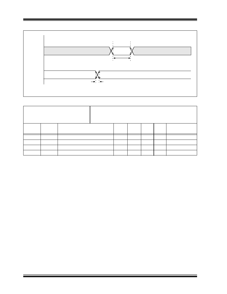
dsPIC30F1010/202X
DS70178A-page 236
Advance Information
©
2006 Microchip Technology Inc.
FIGURE 21-3:
CLKOUT AND I/O TIMING CHARACTERISTICS
TABLE 21-17: CLKOUT AND I/O TIMING REQUIREMENTS
AC CHARACTERISTICS
Standard Operating Conditions: 3.3V and 5.0V (±10%)
(unless otherwise stated)
Operating temperature
-40∞C
T
A
+85∞C for Industrial
-40
∞
C
T
A
+125∞C for Extended
Param
No.
Symbol
Characteristic
(1)(2)(3)
Min
Typ
(4)
Max
Units
Conditions
DO31
T
IO
R
Port output rise time
--
10
25
ns
--
DO32
T
IO
F
Port output fall time
--
10
25
ns
--
DI35
T
INP
INTx pin high or low time (output)
20
--
--
ns
--
DI40
T
RBP
CNx high or low time (input)
2 T
CY
--
--
ns
--
Note 1:
These parameters are asynchronous events not related to any internal clock edges
2:
Measurements are taken in RC mode and EC mode where CLKOUT output is 4 x T
OSC
.
3:
These parameters are characterized but not tested in manufacturing.
4:
Data in "Typ" column is at 5V, 25∞C unless otherwise stated.
Note: Refer to Figure 21-1 for load conditions.
I/O Pin
(Input)
I/O Pin
(Output)
DI35
Old Value
New Value
DI40
DO31
DO32
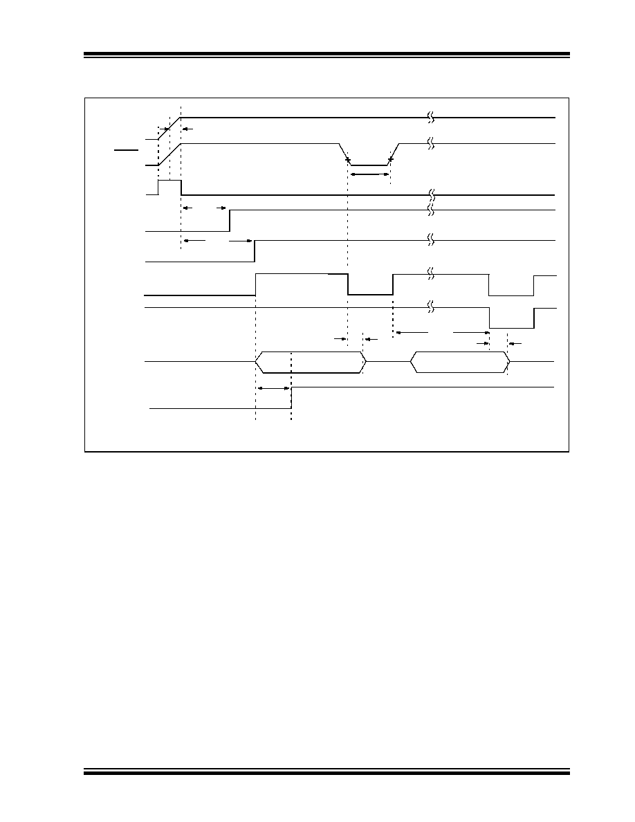
©
2006 Microchip Technology Inc.
Advance Information
DS70178A-page 237
dsPIC30F1010/202X
FIGURE 21-4:
RESET, WATCHDOG TIMER, OSCILLATOR START-UP TIMER AND POWER-UP
TIMER TIMING CHARACTERISTICS
V
DD
MCLR
Internal
POR
PWRT
Time-out
OSC
Time-out
Internal
Reset
Watchdog
Timer
Reset
SY11
SY10
SY20
SY13
I/O Pins
SY13
Note: Refer to Figure 21-1 for load conditions.
FSCM
Delay
SY35
SY30
SY12

dsPIC30F1010/202X
DS70178A-page 238
Advance Information
©
2006 Microchip Technology Inc.
TABLE 21-18: RESET, WATCHDOG TIMER, OSCILLATOR START-UP TIMER, POWER-UP TIMER
AND TIMING REQUIREMENTS
AC CHARACTERISTICS
Standard Operating Conditions: 3.3V and 5.0V (±10%)
(unless otherwise stated)
Operating temperature
-40∞C
T
A
+85∞C for Industrial
-40
∞
C
T
A
+125∞C for Extended
Param
No.
Symbol
Characteristic
(1)
Min
Typ
(2)
Max
Units
Conditions
SY10
TmcL
MCLR Pulse Width (low)
2
--
--
s
-40∞C to +85∞C
SY11
T
PWRT
Power-up Timer Period
TBD
TBD
TBD
TBD
0
4
16
64
TBD
TBD
TBD
TBD
ms
-40∞C to +85∞C
User programmable
SY12
T
POR
Power-On Reset Delay
3
10
30
s
-40∞C to +85∞C
SY13
T
IOZ
I/O High-impedance from MCLR
Low or Watchdog Timer Reset
--
0.8
1.0
s
SY20
T
WDT
1
Watchdog Timer Time-out Period
(No Prescaler)
1.6
2.2
3.0
ms
V
DD
= 5V, -40∞C to +85∞C
T
WDT
2
1.7
2.2
3.1
ms
V
DD
= 3V, -40∞C to +85∞C
SY30
T
OST
Oscillation Start-up Timer Period
--
1024 T
OSC
--
--
T
OSC
= OSC1 period
SY35
T
FSCM
Fail-Safe Clock Monitor Delay
--
500
--
s
-40∞C to +85∞C
Legend: TBD = To Be Determined
Note 1:
These parameters are characterized but not tested in manufacturing.
2:
Data in "Typ" column is at 5V, 25∞C unless otherwise stated.

©
2006 Microchip Technology Inc.
Advance Information
DS70178A-page 239
dsPIC30F1010/202X
FIGURE 21-5:
BAND GAP START-UP TIME CHARACTERISTICS
TABLE 21-19: BAND GAP START-UP TIME REQUIREMENTS
AC CHARACTERISTICS
Standard Operating Conditions: 3.3V and 5.0V (±10%)
(unless otherwise stated)
Operating temperature
-40∞C
T
A
+85∞C for Industrial
-40
∞
C
T
A
+125∞C for Extended
Param
No.
Symbol
Characteristic
(1)
Min
Typ
(2)
Max
Units
Conditions
SY40
T
BGAP
Band Gap Start-up Time
--
40
65
µs
Defined as the time between the
instant that the band gap is enabled
and the moment that the band gap
reference voltage is stable.
RCON<13> status bit.
Note 1:
These parameters are characterized but not tested in manufacturing.
2:
Data in "Typ" column is at 5V, 25∞C unless otherwise stated.
V
BGAP
Enable Band Gap
Band Gap
0V
(see Note)
Stable
Note: Band Gap is enabled when FBORPOR<7> is set.
SY40

dsPIC30F1010/202X
DS70178A-page 240
Advance Information
©
2006 Microchip Technology Inc.
FIGURE 21-6:
TIMER EXTERNAL CLOCK TIMING CHARACTERISTICS
TABLE 21-20: TIMER1 EXTERNAL CLOCK TIMING REQUIREMENTS
AC CHARACTERISTICS
Standard Operating Conditions: 3.3V and 5.0V (±10%)
(unless otherwise stated)
Operating temperature
-40∞C
T
A
+85∞C for Industrial
-40
∞
C
T
A
+125∞C for Extended
Param
No.
Symbol
Characteristic
Min
Typ
Max
Units
Conditions
TA10
T
TX
H
TxCK High Time
Synchronous,
no prescaler
0.5 T
CY
+ 20
--
--
ns
Must also meet
parameter TA15
Synchronous,
with prescaler
10
--
--
ns
Asynchronous
10
--
--
ns
TA11
T
TX
L
TxCK Low Time
Synchronous,
no prescaler
0.5 T
CY
+ 20
--
--
ns
Must also meet
parameter TA15
Synchronous,
with prescaler
10
--
--
ns
Asynchronous
10
--
--
ns
TA15
T
TX
P
TxCK Input Period Synchronous,
no prescaler
T
CY
+ 10
--
--
ns
Synchronous,
with prescaler
Greater of:
20 ns or
(T
CY
+ 40)/N
--
--
--
N = prescale
value
(1, 8, 64, 256)
Asynchronous
20
--
--
ns
OS60
Ft1
SOSC1/T1CK oscillator input
frequency range (oscillator enabled
by setting bit TCS (T1CON, bit 1))
DC
--
50
kHz
TA20
T
CKEXTMRL
Delay from External TxCK Clock
Edge to Timer Increment
0.5 T
CY
1.5 T
CY
--
Tx11
Tx15
Tx10
Tx20
TMRX
OS60
TxCK
Note: "x" refers to Timer Type A or Timer Type B.
Refer to Figure 21-1 for load conditions.

©
2006 Microchip Technology Inc.
Advance Information
DS70178A-page 241
dsPIC30F1010/202X
TABLE 21-21: TIMER2 EXTERNAL CLOCK TIMING REQUIREMENTS
TABLE 21-22: TIMER3 EXTERNAL CLOCK TIMING REQUIREMENTS
AC CHARACTERISTICS
Standard Operating Conditions: 3.3V and 5.0V (±10%)
(unless otherwise stated)
Operating temperature
-40∞C
T
A
+85∞C for Industrial
-40
∞
C
T
A
+125∞C for Extended
Param
No.
Symbol
Characteristic
Min
Typ
Max
Units
Conditions
TB10
TtxH
TxCK High Time
Synchronous,
no prescaler
0.5 T
CY
+ 20
--
--
ns
Must also meet
parameter TB15
Synchronous,
with prescaler
10 --
--
ns
TB11
TtxL
TxCK Low Time
Synchronous,
no prescaler
0.5 T
CY
+ 20
--
--
ns
Must also meet
parameter TB15
Synchronous,
with prescaler
10
--
--
ns
TB15
TtxP
TxCK Input Period Synchronous,
no prescaler
T
CY
+ 10
--
--
ns
N = prescale
value (1, 8, 64, 256)
Synchronous,
with prescaler
Greater of:
20 ns or
(T
CY
+ 40) / N
TB20
T
CKEXTMRL
Delay from External TxCK Clock
Edge to Timer Increment
0.5 T
CY
--
1.5 T
CY
--
AC CHARACTERISTICS
Standard Operating Conditions: 3.3V and 5.0V (±10%)
(unless otherwise stated)
Operating temperature
-40∞C
T
A
+85∞C for Industrial
-40
∞
C
T
A
+125∞C for Extended
Param
No.
Symbol
Characteristic
Min
Typ
Max
Units
Conditions
TC10
TtxH
TxCK High Time
Synchronous
0.5 T
CY
+ 20
--
--
ns
Must also meet
parameter TC15
TC11
TtxL
TxCK Low Time
Synchronous
0.5 T
CY
+ 20
--
--
ns
Must also meet
parameter TC15
TC15
TtxP
TxCK Input Period Synchronous,
no prescaler
T
CY
+ 10
--
--
ns
N = prescale
value (1, 8, 64, 256)
Synchronous,
with prescaler
Greater of:
20 ns or
(T
CY
+ 40) / N
TC20
T
CKEXTMRL
Delay from External TxCK Clock
Edge to Timer Increment
0.5 T
CY
--
1.5 T
CY
--

dsPIC30F1010/202X
DS70178A-page 242
Advance Information
©
2006 Microchip Technology Inc.
FIGURE 21-7:
INPUT CAPTURE (CAPx) TIMING CHARACTERISTICS
TABLE 21-23: INPUT CAPTURE TIMING REQUIREMENTS
FIGURE 21-8:
OUTPUT COMPARE MODULE (OCx) TIMING CHARACTERISTICS
TABLE 21-24: OUTPUT COMPARE MODULE TIMING REQUIREMENTS
AC CHARACTERISTICS
Standard Operating Conditions: 3.3V and 5.0V (±10%)
(unless otherwise stated)
Operating temperature
-40∞C
T
A
+85∞C for Industrial
-40
∞
C
T
A
+125∞C for Extended
Param
No.
Symbol
Characteristic
(1)
Min
Max
Units
Conditions
IC10
TccL
ICx Input Low Time
No Prescaler
0.5 T
CY
+ 20
--
ns
With Prescaler
10
--
ns
IC11
TccH
ICx Input High Time
No Prescaler
0.5 T
CY
+ 20
--
ns
With Prescaler
10
--
ns
IC15
TccP
ICx Input Period
(2 T
CY
+ 40) / N
--
ns
N = prescale
value (1, 4, 16)
Note 1:
These parameters are characterized but not tested in manufacturing.
AC CHARACTERISTICS
Standard Operating Conditions: 3.3V and 5.0V (±10%)
(unless otherwise stated)
Operating temperature
-40∞C
T
A
+85∞C for Industrial
-40
∞
C
T
A
+125∞C for Extended
Param
No.
Symbol
Characteristic
(1)
Min
Typ
(2)
Max
Units
Conditions
OC10
TccF
OCx Output Fall Time
--
--
--
ns
See parameter D032
OC11
TccR
OCx Output Rise Time
--
--
--
ns
See parameter D031
Note 1:
These parameters are characterized but not tested in manufacturing.
2:
Data in "Typ" column is at 5V, 25∞C unless otherwise stated. Parameters are for design guidance only and
are not tested.
IC
X
IC10
IC11
IC15
Note: Refer to Figure 21-1 for load conditions.
OCx
OC11
OC10
(Output Compare
Note: Refer to Figure 21-1 for load conditions.
or PWM Mode)
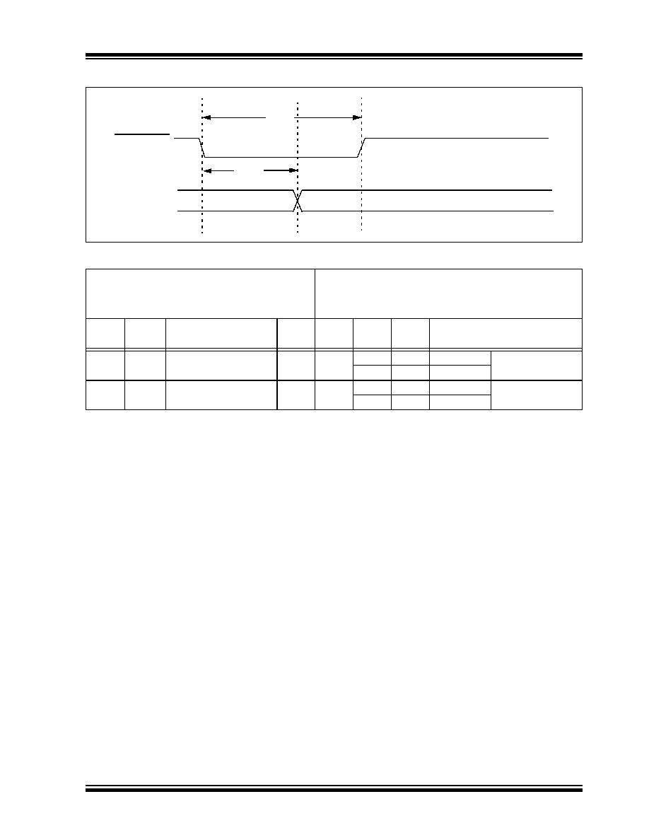
©
2006 Microchip Technology Inc.
Advance Information
DS70178A-page 243
dsPIC30F1010/202X
FIGURE 21-9:
OC/PWM MODULE TIMING CHARACTERISTICS
TABLE 21-25: SIMPLE OC/PWM MODE TIMING REQUIREMENTS
AC CHARACTERISTICS
Standard Operating Conditions: 3.3V and 5.0V (±10%)
(unless otherwise stated)
Operating temperature
-40∞C
T
A
+85∞C for Industrial
-40
∞
C
T
A
+125∞C for Extended
Param
No.
Symbol
Characteristic
(1)
Min
Typ
(2)
Max
Units
Conditions
OC15
T
FD
Fault Input to PWM I/O
Change
--
--
25
ns
V
DD
= 3V
-40∞C to +85∞C
TBD
ns
V
DD
= 5V
OC20
T
FLT
Fault Input Pulse Width
--
--
50
ns
V
DD
= 3V
-40∞C to +85∞C
TBD
ns
V
DD
= 5V
Legend: TBD = To Be Determined
Note 1:
These parameters are characterized but not tested in manufacturing.
2:
Data in "Typ" column is at 5V, 25∞C unless otherwise stated. Parameters are for design guidance only and
are not tested.
OCFA/OCFB
OCx
OC20
OC15

dsPIC30F1010/202X
DS70178A-page 244
Advance Information
©
2006 Microchip Technology Inc.
FIGURE 21-10:
SMPS PWM MODULE FAULT TIMING CHARACTERISTICS
FIGURE 21-11:
MOTOR CONTROL PWM MODULE TIMING CHARACTERISTICS
TABLE 21-26: MOTOR CONTROL PWM MODULE TIMING REQUIREMENTS
AC CHARACTERISTICS
Standard Operating Conditions: 3.3V and 5.0V (±10%)
(unless otherwise stated)
Operating temperature
-40∞C
T
A
+85∞C for Industrial
-40
∞
C
T
A
+125∞C for Extended
Param
No.
Symbol
Characteristic
(1)
Min
Typ
(2)
Max
Units
Conditions
MP10
T
F
PWM
PWM Output Fall Time
--
10
25
ns
V
DD
= 5V
-40∞C to +85∞C
MP11
T
R
PWM
PWM Output Rise Time
--
10
25
ns
V
DD
= 5V
-40∞C to +85∞C
MP12
T
F
PWM
PWM Output Fall Time
--
TBD
TBD
ns
V
DD
= 3V
-40∞C to +85∞C
MP13
T
R
PWM
PWM Output Rise Time
--
TBD
TBD
ns
V
DD
= 3V
-40∞C to +85∞C
MP20
T
FD
Fault Input
to PWM
I/O Change
--
--
25
ns
V
DD
= 3V
-40∞C to +85∞C
TBD
ns
V
DD
= 5V
MP30
T
FH
Minimum Pulse Width
--
--
50
ns
V
DD
= 3V
-40∞C to +85∞C
TBD
ns
V
DD
= 5V
Legend: TBD = To Be Determined
Note 1:
These parameters are characterized but not tested in manufacturing.
2:
Data in "Typ" column is at 5V, 25∞C unless otherwise stated. Parameters are for design guidance only and
are not tested.
FLTA/B
PWMx
MP30
MP20
PWMx
MP11 MP10
Note: Refer to Figure 21-1 for load conditions.
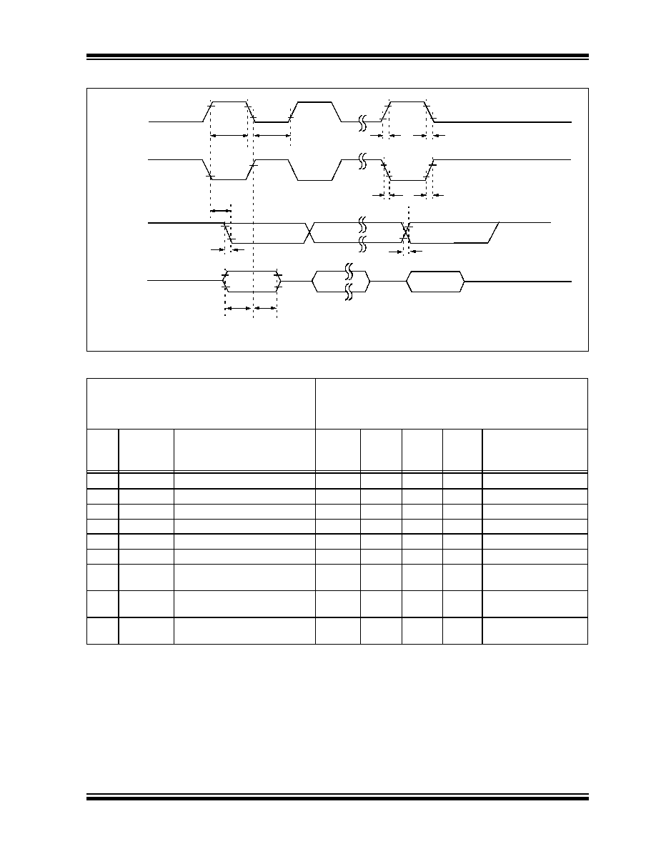
©
2006 Microchip Technology Inc.
Advance Information
DS70178A-page 245
dsPIC30F1010/202X
FIGURE 21-12:
SPI MODULE MASTER MODE (CKE =
0
) TIMING CHARACTERISTICS
TABLE 21-27: SPI MASTER MODE (CKE =
0
) TIMING REQUIREMENTS
AC CHARACTERISTICS
Standard Operating Conditions: 3.3V and 5.0V (±10%)
(unless otherwise stated)
Operating temperature
-40∞C
T
A
+85∞C for Industrial
-40
∞
C
T
A
+125∞C for Extended
Para
m
No.
Symbol
Characteristic
(1)
Min
Typ
(2)
Max
Units
Conditions
SP10 TscL
SCK
X
Output Low Time
(3)
T
CY
/ 2
--
--
ns
--
SP11 TscH
SCK
X
Output High Time
(3)
T
CY
/ 2
--
--
ns
--
SP20 TscF
SCK
X
Output Fall Time
(4)
--
--
--
ns
See parameter D032
SP21 TscR
SCK
X
Output Rise Time
(4)
--
--
--
ns
See parameter D031
SP30 TdoF
SDO
X
Data Output Fall Time
(4)
--
--
--
ns
See parameter D032
SP31 TdoR
SDO
X
Data Output Rise Time
(4)
--
--
--
ns
See parameter D031
SP35 TscH2doV,
TscL2doV
SDO
X
Data Output Valid after
SCK
X
Edge
--
--
30
ns
--
SP40 TdiV2scH,
TdiV2scL
Setup Time of SDI
X
Data Input
to SCK
X
Edge
20
--
--
ns
--
SP41 TscH2diL,
TscL2diL
Hold Time of SDI
X
Data Input
to SCK
X
Edge
20
--
--
ns
--
Note 1:
These parameters are characterized but not tested in manufacturing.
2:
Data in "Typ" column is at 5V, 25∞C unless otherwise stated. Parameters are for design guidance only and
are not tested.
3:
The minimum clock period for SCK is 100 ns. Therefore, the clock generated in Master mode must not
violate this specification.
4:
Assumes 50 pF load on all SPI pins.
SCKx
(CKP =
0
)
SCKx
(CKP =
1
)
SDOx
SDIx
SP11
SP10
SP40 SP41
SP21
SP20
SP35
SP20
SP21
MSb
LSb
BIT14 - - - - - -1
MSb IN
LSb IN
BIT14 - - - -1
SP30
SP31
Note: Refer to Figure 21-1 for load conditions.
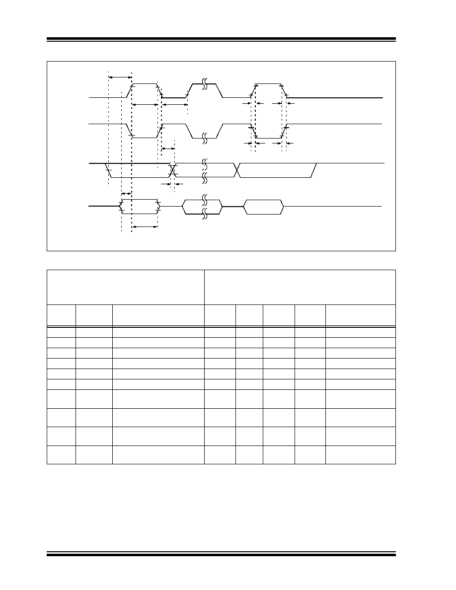
dsPIC30F1010/202X
DS70178A-page 246
Advance Information
©
2006 Microchip Technology Inc.
FIGURE 21-13:
SPI MODULE MASTER MODE (CKE =
1
) TIMING CHARACTERISTICS
TABLE 21-28: SPI MODULE MASTER MODE (CKE =
1
) TIMING REQUIREMENTS
AC CHARACTERISTICS
Standard Operating Conditions: 3.3V and 5.0V (±10%)
(unless otherwise stated)
Operating temperature
-40∞C
T
A
+85∞C for Industrial
-40
∞
C
T
A
+125∞C for Extended
Param
No.
Symbol
Characteristic
(1)
Min
Typ
(2)
Max
Units
Conditions
SP10
TscL
SCK
X
output low time
(3)
T
CY
/ 2
--
--
ns
--
SP11
TscH
SCK
X
output high time
(3)
T
CY
/ 2
--
--
ns
--
SP20
TscF
SCK
X
output fall time
(4)
--
--
--
ns
See parameter D032
SP21
TscR
SCK
X
output rise time
(4)
--
--
--
ns
See parameter D031
SP30
TdoF
SDO
X
data output fall time
(4)
--
--
--
ns
See parameter D032
SP31
TdoR
SDO
X
data output rise time
(4)
--
--
--
ns
See parameter D031
SP35
TscH2doV,
TscL2doV
SDO
X
data output valid after
SCK
X
edge
--
--
30
ns
--
SP36
TdoV2sc,
TdoV2scL
SDO
X
data output setup to
first SCK
X
edge
30
--
--
ns
--
SP40
TdiV2scH,
TdiV2scL
Setup time of SDI
X
data input
to SCK
X
edge
20
--
--
ns
--
SP41
TscH2diL,
TscL2diL
Hold time of SDI
X
data input
to SCK
X
edge
20
--
--
ns
--
Note 1:
These parameters are characterized but not tested in manufacturing.
2:
Data in "Typ" column is at 5V, 25∞C unless otherwise stated. Parameters are for design guidance only and
are not tested.
3:
The minimum clock period for SCK is 100 ns. Therefore, the clock generated in Master mode must not
violate this specification.
4:
Assumes 50 pF load on all SPI pins.
SCK
X
(CKP =
0
)
SCK
X
(CKP =
1
)
SDO
X
SDI
X
SP36
SP30,SP31
SP35
MSb
MSb IN
BIT14 - - - - - -1
LSb IN
BIT14 - - - -1
LSb
Note: Refer to Figure 21-1 for load conditions.
SP11
SP10
SP20
SP21
SP21
SP20
SP40
SP41
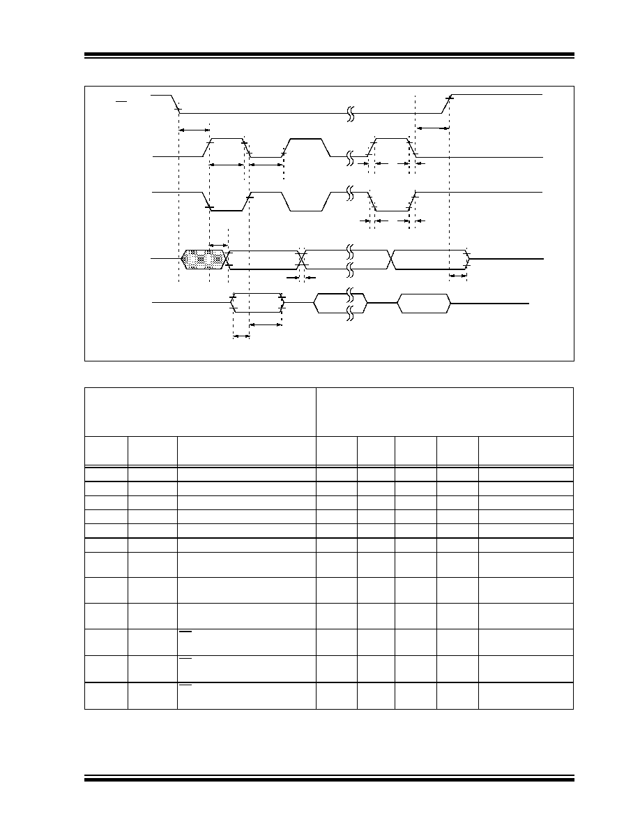
©
2006 Microchip Technology Inc.
Advance Information
DS70178A-page 247
dsPIC30F1010/202X
FIGURE 21-14:
SPI MODULE SLAVE MODE (CKE =
0
) TIMING CHARACTERISTICS
TABLE 21-29: SPI MODULE SLAVE MODE (CKE =
0
) TIMING REQUIREMENTS
AC CHARACTERISTICS
Standard Operating Conditions: 3.3V and 5.0V (±10%)
(unless otherwise stated)
Operating temperature
-40∞C
T
A
+85∞C for Industrial
-40
∞
C
T
A
+125∞C for Extended
Param
No.
Symbol
Characteristic
(1)
Min
Typ
(2)
Max
Units
Conditions
SP70
TscL
SCK
X
Input Low Time
30
--
--
ns
--
SP71
TscH
SCK
X
Input High Time
30
--
--
ns
--
SP72
TscF
SCK
X
Input Fall Time
(3)
--
10
25
ns
--
SP73
TscR
SCK
X
Input Rise Time
(3)
--
10
25
ns
--
SP30
TdoF
SDO
X
Data Output Fall Time
(3)
--
--
--
ns
See parameter D032
SP31
TdoR
SDO
X
Data Output Rise Time
(3)
--
--
--
ns
See parameter D031
SP35
TscH2doV,
TscL2doV
SDO
X
Data Output Valid after
SCK
X
Edge
--
--
30
ns
--
SP40
TdiV2scH,
TdiV2scL
Setup Time of SDI
X
Data Input
to SCK
X
Edge
20
--
--
ns
--
SP41
TscH2diL,
TscL2diL
Hold Time of SDI
X
Data Input
to SCK
X
Edge
20
--
--
ns
--
SP50
TssL2scH,
TssL2scL
SS
X
to SCK
X
or SCK
X
Input
120
--
--
ns
--
SP51
TssH2doZ SS
X
to SDO
X
Output
High-impedance
(3)
10
--
50
ns
--
SP52
TscH2ssH
TscL2ssH
SS
X
after SCK Edge
1.5 T
CY
+ 40
--
--
ns
--
Note 1:
These parameters are characterized but not tested in manufacturing.
2:
Data in "Typ" column is at 5V, 25∞C unless otherwise stated. Parameters are for design guidance only and
are not tested.
3:
Assumes 50 pF load on all SPI pins.
SS
X
SCK
X
(CKP =
0
)
SCK
X
(CKP =
1
)
SDO
X
SDI
SP50
SP40
SP41
SP30,SP31
SP51
SP35
SDI
X
MSb
LSb
BIT14 - - - - - -1
MSb IN
BIT14 - - - -1
LSb IN
SP52
SP73
SP72
SP72
SP73
SP71
SP70
Note: Refer to Figure 21-1 for load conditions.

dsPIC30F1010/202X
DS70178A-page 248
Advance Information
©
2006 Microchip Technology Inc.
FIGURE 21-15:
SPI MODULE SLAVE MODE (CKE =
1
) TIMING CHARACTERISTICS
SS
X
SCK
X
(CKP =
0
)
SCK
X
(CKP =
1
)
SDO
X
SDI
SP50
SP60
SDI
X
SP30,SP31
MSb
BIT14 - - - - - -1
LSb
SP51
MSb IN
BIT14 - - - -1
LSb IN
SP35
SP52
SP52
SP73
SP72
SP72
SP73
SP71
SP70
SP40
SP41
Note: Refer to Figure 21-1 for load conditions.

©
2006 Microchip Technology Inc.
Advance Information
DS70178A-page 249
dsPIC30F1010/202X
TABLE 21-30: SPI MODULE SLAVE MODE (CKE =
1
) TIMING REQUIREMENTS
AC CHARACTERISTICS
Standard Operating Conditions: 3.3V and 5.0V (±10%)
(unless otherwise stated)
Operating temperature
-40∞C
T
A
+85∞C for Industrial
-40
∞
C
T
A
+125∞C for Extended
Param
No.
Symbol
Characteristic
(1)
Min
Typ
(2)
Max
Units
Conditions
SP70
TscL
SCK
X
Input Low Time
30
--
--
ns
--
SP71
TscH
SCK
X
Input High Time
30
--
--
ns
--
SP72
TscF
SCK
X
Input Fall Time
(3)
--
10
25
ns
--
SP73
TscR
SCK
X
Input Rise Time
(3)
--
10
25
ns
--
SP30
TdoF
SDO
X
Data Output Fall Time
(3)
--
--
--
ns
See parameter D032
SP31
TdoR
SDO
X
Data Output Rise Time
(3)
--
--
--
ns
See parameter D031
SP35
TscH2doV,
TscL2doV
SDO
X
Data Output Valid after
SCK
X
Edge
--
--
30
ns
--
SP40
TdiV2scH,
TdiV2scL
Setup Time of SDI
X
Data Input
to SCK
X
Edge
20
--
--
ns
--
SP41
TscH2diL,
TscL2diL
Hold Time of SDI
X
Data Input
to SCK
X
Edge
20
--
--
ns
--
SP50
TssL2scH,
TssL2scL
SS
X
to SCK
X
or SCK
X
input
120
--
--
ns
--
SP51
TssH2doZ SS
to SDO
X
Output
High-impedance
(4)
10
--
50
ns
--
SP52
TscH2ssH
TscL2ssH
SS
X
after SCK
X
Edge
1.5 T
CY
+
40
--
--
ns
--
SP60
TssL2doV SDO
X
Data Output Valid after
SS
X
Edge
--
--
50
ns
--
Note 1:
These parameters are characterized but not tested in manufacturing.
2:
Data in "Typ" column is at 5V, 25∞C unless otherwise stated. Parameters are for design guidance only and
are not tested.
3:
The minimum clock period for SCK is 100 ns. Therefore, the clock generated in Master mode must not
violate this specification.
4:
Assumes 50 pF load on all SPI pins.

dsPIC30F1010/202X
DS70178A-page 250
Advance Information
©
2006 Microchip Technology Inc.
FIGURE 21-16:
I
2
CTM BUS START/STOP BITS TIMING CHARACTERISTICS (MASTER MODE)
FIGURE 21-17:
I
2
CTM BUS DATA TIMING CHARACTERISTICS (MASTER MODE)
IM31
IM34
SCL
SDA
Start
Condition
Stop
Condition
IM30
IM33
Note: Refer to Figure 21-1 for load conditions.
IM11
IM10
IM33
IM11
IM10
IM20
IM26
IM25
IM40
IM40
IM45
IM21
SCL
SDA
In
SDA
Out
Note: Refer to Figure 21-1 for load conditions.

©
2006 Microchip Technology Inc.
Advance Information
DS70178A-page 251
dsPIC30F1010/202X
TABLE 21-31: I
2
CTM BUS DATA TIMING REQUIREMENTS (MASTER MODE)
AC CHARACTERISTICS
Standard Operating Conditions: 3.3V and 5.0V (±10%)
(unless otherwise stated)
Operating temperature
-40∞C
T
A
+85∞C for Industrial
-40
∞
C
T
A
+125∞C for Extended
Param
No.
Symbol
Characteristic
Min
(1)
Max
Units
Conditions
IM10
T
LO
:
SCL
Clock Low Time
100 kHz mode
T
CY
/ 2 (BRG + 1)
--
µs
--
400 kHz mode
T
CY
/ 2 (BRG + 1)
--
µs
--
1 MHz mode
(2)
T
CY
/ 2 (BRG + 1)
--
µs
--
IM11
T
HI
:
SCL
Clock High Time 100 kHz mode
T
CY
/ 2 (BRG + 1)
--
µs
--
400 kHz mode
T
CY
/ 2 (BRG + 1)
--
µs
--
1 MHz mode
(2)
T
CY
/ 2 (BRG + 1)
--
µs
--
IM20
T
F
:
SCL
SDA and SCL
Fall Time
100 kHz mode
--
300
ns
C
B
is specified to be
from 10 to 400 pF
400 kHz mode
20 + 0.1 C
B
300
ns
1 MHz mode
(2)
--
100
ns
IM21
T
R
:
SCL
SDA and SCL
Rise Time
100 kHz mode
--
1000
ns
C
B
is specified to be
from 10 to 400 pF
400 kHz mode
20 + 0.1 C
B
300 ns
1 MHz mode
(2)
--
300
ns
IM25
T
SU
:
DAT
Data Input
Setup Time
100 kHz mode
250
--
ns
--
400 kHz mode
100
--
ns
1 MHz mode
(2)
TBD --
ns
IM26
T
HD
:
DAT
Data Input
Hold Time
100 kHz mode
0
--
ns
--
400 kHz mode
0
0.9
µs
1 MHz mode
(2)
TBD --
ns
IM30
T
SU
:
STA
Start Condition
Setup Time
100 kHz mode
T
CY
/ 2 (BRG + 1)
--
µs
Only relevant for
repeated Start
condition
400 kHz mode
T
CY
/ 2 (BRG + 1)
--
µs
1 MHz mode
(2)
T
CY
/ 2 (BRG + 1)
--
µs
IM31
T
HD
:
STA
Start Condition
Hold Time
100 kHz mode
T
CY
/ 2 (BRG + 1)
--
µs
After this period the
first clock pulse is
generated
400 kHz mode
T
CY
/ 2 (BRG + 1)
--
µs
1 MHz mode
(2)
T
CY
/ 2 (BRG + 1)
--
µs
IM33
T
SU
:
STO
Stop Condition
Setup Time
100 kHz mode
T
CY
/ 2 (BRG + 1)
--
µs
--
400 kHz mode
T
CY
/ 2 (BRG + 1)
--
µs
1 MHz mode
(2)
T
CY
/ 2 (BRG + 1)
--
µs
IM34
T
HD
:
STO
Stop Condition
100 kHz mode
T
CY
/ 2 (BRG + 1)
--
ns
--
Hold Time
400 kHz mode
T
CY
/ 2 (BRG + 1)
--
ns
1 MHz mode
(2)
T
CY
/ 2 (BRG + 1)
--
ns
IM40
T
AA
:
SCL
Output Valid
From Clock
100 kHz mode
--
3500
ns
--
400 kHz mode
--
1000
ns
--
1 MHz mode
(2)
--
--
ns
--
IM45
T
BF
:
SDA
Bus Free Time
100 kHz mode
4.7
--
µs
Time the bus must be
free before a new
transmission can start
400 kHz mode
1.3
--
µs
1 MHz mode
(2)
TBD
--
µs
IM50
C
B
Bus Capacitive Loading
--
400
pF
Legend: TBD = To Be Determined
Note 1:
BRG is the value of the I
2
CTM Baud Rate Generator. Refer to Section 21 "Inter-Integrated CircuitTM
(I
2
C)" in the "dsPIC30F Family Reference Manual" (DS70046).
2:
Maximum pin capacitance = 10 pF for all I
2
C pins (for 1 MHz mode only).

dsPIC30F1010/202X
DS70178A-page 252
Advance Information
©
2006 Microchip Technology Inc.
FIGURE 21-18:
I
2
CTM BUS START/STOP BITS TIMING CHARACTERISTICS (SLAVE MODE)
FIGURE 21-19:
I
2
CTM BUS DATA TIMING CHARACTERISTICS (SLAVE MODE)
IS31
IS34
SCL
SDA
Start
Condition
Stop
Condition
IS30
IS33
IS30
IS31
IS33
IS11
IS10
IS20
IS26
IS25
IS40
IS40
IS45
IS21
SCL
SDA
In
SDA
Out

©
2006 Microchip Technology Inc.
Advance Information
DS70178A-page 253
dsPIC30F1010/202X
TABLE 21-32: I
2
CTM BUS DATA TIMING REQUIREMENTS (SLAVE MODE)
AC CHARACTERISTICS
Standard Operating Conditions: 3.3V and 5.0V (±10%)
(unless otherwise stated)
Operating temperature
-40∞C
T
A
+85∞C for Industrial
-40
∞
C
T
A
+125∞C for Extended
Param
No.
Symbol
Characteristic
Min
Max
Units
Conditions
IS10
T
LO
:
SCL
Clock Low Time
100 kHz mode
4.7
--
s
Device must operate at a
minimum of 1.5 MHz
400 kHz mode
1.3
--
s
Device must operate at a
minimum of 10 MHz.
1 MHz mode
(1)
0.5
--
s
--
IS11
T
HI
:
SCL
Clock High Time
100 kHz mode
4.0
--
s
Device must operate at a
minimum of 1.5 MHz
400 kHz mode
0.6
--
s
Device must operate at a
minimum of 10 MHz
1 MHz mode
(1)
0.5
--
s
--
IS20
T
F
:
SCL
SDA and SCL
Fall Time
100 kHz mode
--
300
ns
C
B
is specified to be from
10 to 400 pF
400 kHz mode
20 + 0.1 C
B
300
ns
1 MHz mode
(1)
--
100
ns
IS21
T
R
:
SCL
SDA and SCL
Rise Time
100 kHz mode
--
1000
ns
C
B
is specified to be from
10 to 400 pF
400 kHz mode
20 + 0.1 C
B
300
ns
1 MHz mode
(1)
--
300
ns
IS25
T
SU
:
DAT
Data Input
Setup Time
100 kHz mode
250
--
ns
--
400 kHz mode
100
--
ns
1 MHz mode
(1)
100
--
ns
IS26
T
HD
:
DAT
Data Input
Hold Time
100 kHz mode
0
--
ns
--
400 kHz mode
0
0.9
s
1 MHz mode
(1)
0
0.3
s
IS30
T
SU
:
STA
Start Condition
Setup Time
100 kHz mode
4.7
--
s
Only relevant for repeated
Start condition
400 kHz mode
0.6
--
s
1 MHz mode
(1)
0.25
--
s
IS31
T
HD
:
STA
Start Condition
Hold Time
100 kHz mode
4.0
--
s
After this period the first
clock pulse is generated
400 kHz mode
0.6
--
s
1 MHz mode
(1)
0.25
--
s
IS33
T
SU
:
STO
Stop Condition
Setup Time
100 kHz mode
4.7
--
s
--
400 kHz mode
0.6
--
s
1 MHz mode
(1)
0.6
--
s
IS34
T
HD
:
STO
Stop Condition
100 kHz mode
4000
--
ns
--
Hold Time
400 kHz mode
600
--
ns
1 MHz mode
(1)
250
ns
IS40
T
AA
:
SCL
Output Valid From
Clock
100 kHz mode
0
3500
ns
--
400 kHz mode
0
1000
ns
1 MHz mode
(1)
0
350
ns
IS45
T
BF
:
SDA
Bus Free Time
100 kHz mode
4.7
--
s
Time the bus must be free
before a new transmission
can start
400 kHz mode
1.3
--
s
1 MHz mode
(1)
0.5
--
s
IS50
C
B
Bus Capacitive
Loading
--
400
pF
--
Note 1:
Maximum pin capacitance = 10 pF for all I
2
CTM pins (for 1 MHz mode only).

dsPIC30F1010/202X
DS70178A-page 254
Advance Information
©
2006 Microchip Technology Inc.
TABLE 21-33: 10-BIT HIGH-SPEED A/D MODULE SPECIFICATIONS
AC CHARACTERISTICS
Standard Operating Conditions: 3.3V and 5.0V (±10%)
(unless otherwise stated)
Operating temperature
-40∞C
T
A
+85∞C for Industrial
-40
∞
C
T
A
+125∞C for Extended
Param
No.
Symbol
Characteristic
Min.
Typ
Max.
Units
Conditions
Device Supply
AD01
AV
DD
Module V
DD
Supply
Greater of
V
DD
≠ 0.3
or 2.7
Lesser of
V
DD
+ 0.3
or 5.5
V
--
AD02
AV
SS
Module V
SS
Supply
Vss ≠ 0.3
V
SS
+ 0.3
V
--
Reference Inputs
AD05
V
REFH
Reference Voltage High
AVss + 2.7
AV
DD
V
--
AD06
V
REFL
Reference Voltage Low
AVss
AV
DD
≠ 2.7
V
--
AD07
V
REF
Absolute Reference Voltage AVss ≠ 0.3
AV
DD
+ 0.3
V
--
AD08
I
REF
Current Drain
--
200
.001
300
3
A
A
A/D operating
A/D off
Analog Input
AD10
V
INH
-V
INL
Full-Scale Input Span
V
REFL
V
REFH
V
--
AD11
V
IN
Absolute Input Voltage
AV
SS
≠ 0.3
AV
DD
+ 0.3
V
--
AD12
--
Leakage Current
--
±0.001
±0.244
A
V
INL
= AV
SS
= V
REFL
= 0V,
AV
DD
= V
REFH
= 5V
Source Impedance = 5 k
AD13
--
Leakage Current
--
±0.001
±0.244
A
V
INL
= AV
SS
= V
REFL
= 0V,
AV
DD
= V
REFH
= 3V
Source Impedance = 5 k
AD15
R
SS
Switch Resistance
--
3.2K
--
--
AD16
C
SAMPLE
Sample Capacitor
--
4.4
pF
--
AD17
R
IN
Recommended Impedance
Of Analog Voltage Source
--
5K
--
DC Accuracy
AD20
Nr
Resolution
10 data bits
bits
--
AD21
INL
Integral Nonlinearity
--
±0.5
< ±1
LSb
V
INL
= AV
SS
= V
REFL
= 0V,
AV
DD
= V
REFH
= 5V
AD21A INL
Integral Nonlinearity
--
±0.5
< ±1
LSb
V
INL
= AV
SS
= V
REFL
= 0V,
AV
DD
= V
REFH
= 3V
AD22
DNL
Differential Nonlinearity
--
±0.5
< ±1
LSb
V
INL
= AV
SS
= V
REFL
= 0V,
AV
DD
= V
REFH
= 5V
AD22A DNL
Differential Nonlinearity
--
±0.5
< ±1
LSb
V
INL
= AV
SS
= V
REFL
= 0V,
AV
DD
= V
REFH
= 3V
AD23
G
ERR
Gain Error
--
±0.75
TBD
LSb
V
INL
= AV
SS
= V
REFL
= 0V,
AV
DD
= V
REFH
= 5V
AD23A G
ERR
Gain Error
--
±0.75
TBD
LSb
V
INL
= AV
SS
= V
REFL
= 0V,
AV
DD
= V
REFH
= 3V
Legend: TBD = To Be Determined
Note 1:
Because the sample caps will eventually lose charge, clock rates below 10 kHz can affect linearity
performance, especially at elevated temperatures.
2:
The A/D conversion result never decreases with an increase in the input voltage, and has no missing
codes.

©
2006 Microchip Technology Inc.
Advance Information
DS70178A-page 255
dsPIC30F1010/202X
FIGURE 21-20:
A/D CONVERSION TIMING PER INPUT
AD24
E
OFF
Offset Error
--
±0.75
TBD
LSb
V
INL
= AV
SS
= V
REFL
= 0V,
AV
DD
= V
REFH
= 5V
AD24A E
OFF
Offset Error
--
±0.75
TBD
LSb
V
INL
= AV
SS
= V
REFL
= 0V,
AV
DD
= V
REFH
= 3V
AD25
--
Monotonicity
(2)
--
--
--
--
Guaranteed
Dynamic Performance
AD30
THD
Total Harmonic Distortion
--
TBD
--
dB
--
AD31
SINAD
Signal to Noise and
Distortion
--
TBD
--
dB
--
AD32
SFDR
Spurious Free Dynamic
Range
--
TBD
--
dB
--
AD33
F
NYQ
Input Signal Bandwidth
--
--
1
MHz
--
AD34
ENOB
Effective Number of Bits
--
TBD
TBD
bits
--
TABLE 21-33: 10-BIT HIGH-SPEED A/D MODULE SPECIFICATIONS (CONTINUED)
AC CHARACTERISTICS
Standard Operating Conditions: 3.3V and 5.0V (±10%)
(unless otherwise stated)
Operating temperature
-40∞C
T
A
+85∞C for Industrial
-40
∞
C
T
A
+125∞C for Extended
Param
No.
Symbol
Characteristic
Min.
Typ
Max.
Units
Conditions
Legend: TBD = To Be Determined
Note 1:
Because the sample caps will eventually lose charge, clock rates below 10 kHz can affect linearity
performance, especially at elevated temperatures.
2:
The A/D conversion result never decreases with an increase in the input voltage, and has no missing
codes.
T
AD
A/D Data
ADBUFxx
9
0
2
1
0
Old Data
New Data
CONV
A/D Clock
Trigger Pulse
Tconv

dsPIC30F1010/202X
DS70178A-page 256
Advance Information
©
2006 Microchip Technology Inc.
TABLE 21-34: COMPARATOR OPERATING CONDITIONS
TABLE 21-35: COMPARATOR AC AND DC SPECIFICATIONS
TABLE 21-36: DAC DC SPECIFICATIONS
TABLE 21-37: DAC AC SPECIFICATIONS
Sym
Characteristic
Min
Typ
Max
Units
Comments
V
DD
Voltage Range
3.0
--
3.6
V
Operating range of 3.0 V-3.6V
V
DD
Voltage Range
4.5
--
5.5
V
Operating range of 4.5 V-5.5 V
T
EMP
Temperature Range
-40
--
105
∞C
Note that junction temperature can exceed
125∞C under these ambient conditions.
Standard Operating Conditions (unless otherwise stated)
Operating temperature: -40∞C
T
A
+105∞C
Sym
Characteristic
Min
Typ
Max
Units
Comments
V
IOFF
Input offset voltage
±5
±15
mV
V
ICM
Input common mode voltage
range
0
V
DD
≠
1.5
V
V
GAIN
Open Loop gain
90
db
CMRR
Common mode rejection
ratio
70
db
T
RESP
Large signal response
20
30
ns
V+ input step of 100mv while V- input held
at AV
DD
/2. Delay measured from analog
input pin to PWM output pin.
Standard Operating Conditions (unless otherwise stated)
Operating temperature: -40∞C
T
A
+105∞C
Sym
Characteristic
Min
Typ
Max
Units
Comments
CV
RSRC
Input reference voltage
0
AV
DD
≠
1.6
V
CV
RES
Resolution
10
Bits
INL
DNL
Transfer Function Accuracy
Integral Non-Linearity Error
Differential Non-Linearity Error
Offset Error
Gain Error
TBD
TBD
TBD
TBD
1
0.8
±2
2.0
TBD
TBD
TBD
TBD
LSB
LSB
LSB
LSB
AV
DD
= 5 V,
DACREF
= (AV
DD
/2) V
Legend: TBD = To Be Determined
Standard Operating Conditions (unless otherwise stated)
Operating temperature: -40∞C
T
A
+125∞C
Sym
Characteristic
Min
Typ
Max
Units
Comments
T
SET
Settling Time
2.0
µs
Measured when range = 1 (High
Range), and cmref<9:0> transitions from
0x1FF to 0x300.

©
2006 Microchip Technology Inc.
Advance Information
DS70178A-page 257
dsPIC30F1010/202X
22.0
PACKAGE MARKING INFORMATION
XXXXXXXXXXXXXXXXX
YYWWNNN
28-Lead PDIP (Skinny DIP)
Example
XXXXXXXXXXXXXXXXX
0348017
dsPIC30F202X-30I/SP
28-Lead SOIC
YYWWNNN
Example
XXXXXXXXXXXXXXXXXXXX
XXXXXXXXXXXXXXXXXXXX
XXXXXXXXXXXXXXXXXXXX
0348017
dsPIC30F202X-30I/SO
Note:
In the event the full Microchip part number cannot be marked on one line, it will
be carried over to the next line thus limiting the number of available characters
for customer specific information.
* Standard device marking consists of Microchip part number, year code, week code and traceability code.
For device marking beyond this, certain price adders apply. Please check with your Microchip Sales Office.
For QTP devices, any special marking adders are included in QTP price.
28-Lead QFN-S
XXXXXXX
XXXXXXX
YYWWNNN
Example
dsPIC30F1010
-30I/MM
040700U
44-Lead TQFP
XXXXXXXXXX
XXXXXXXXXX
XXXXXXXXXX
YYWWNNN
Example
dsPIC30F202X
-I/PT
0510017
Legend: XX...X
Customer specific information*
Y
Year code (last digit of calendar year)
YY
Year code (last 2 digits of calendar year)
WW
Week code (week of January 1 is week `01')
NNN
Alphanumeric traceability code
XXXXXXXXXX
44-Lead QFN
XXXXXXXXXX
XXXXXXXXXX
YYWWNNN
dsPIC30F202X
Example
-I/ML
0510017
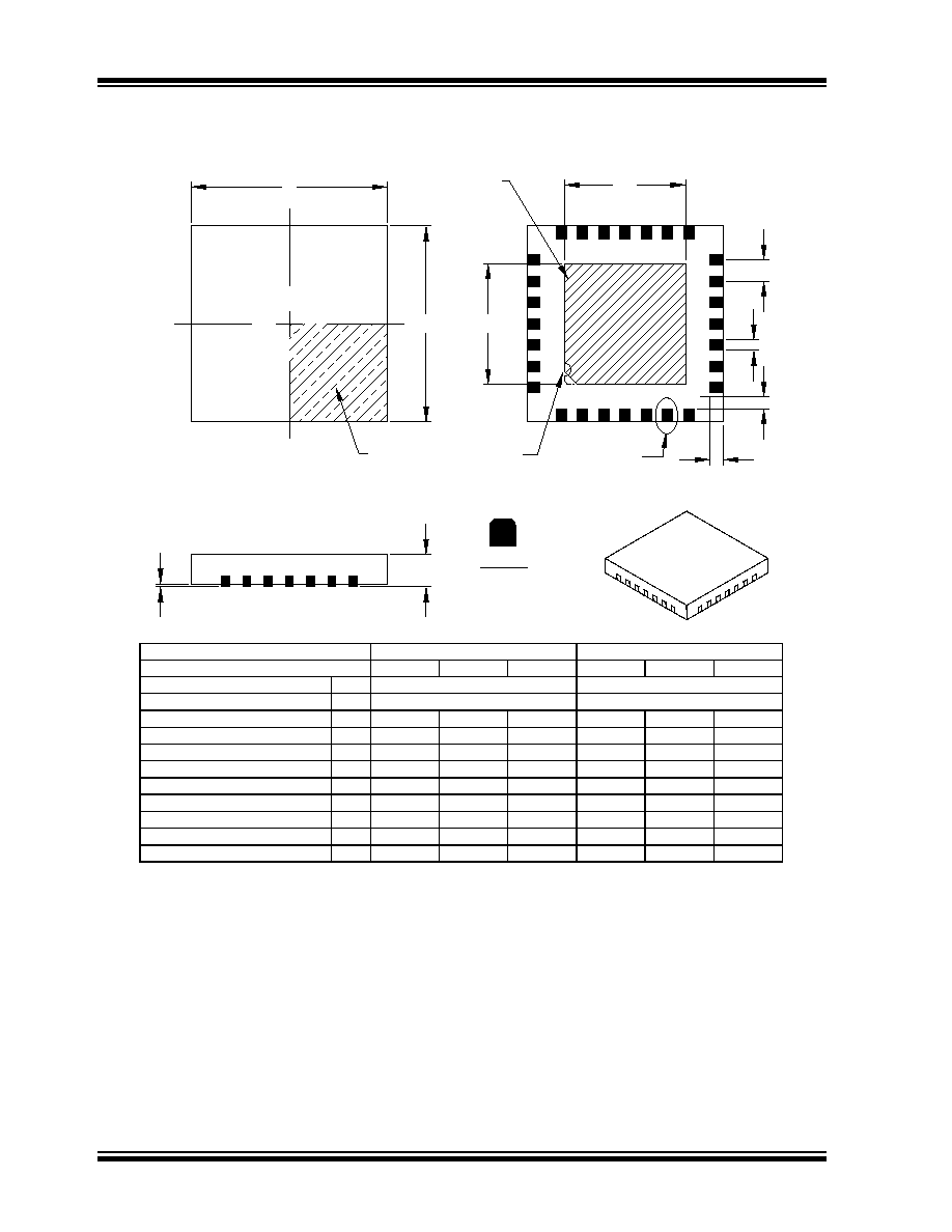
dsPIC30F1010/202X
DS70178A-page 258
Advance Information
©
2006 Microchip Technology Inc.
28-Lead Plastic Quad Flat No Lead Package (MM) 6x6x0.9 mm Body (QFN-S) ≠
With 0.40 mm Contact Length (Saw Singulated)
E2
E
D
D2
2
1
2
1
e
b
K
n
L
EXPOSED
METAL
PAD
(NOTE 2)
OPTIONAL
INDEX
AREA
(NOTE 1)
ALTERNATE
INDEX
INDICATORS
SEE DETAIL
BOTTOM VIEW
TOP VIEW
A
A1
DETAIL
ALTERNATE
PAD OUTLINE
INCHES
NOM
.026 BSC
Number of Pins
Overall Width
Overall Length
Overall Height
Contact Length ß
Exposed Pad Width
Exposed Pad Length
* Controlling Parameter
Lead Width
Notes:
Standoff
Pitch
D2
.144
.232
.013
.012
b
L
D
Units
Dimension Limits
A1
E2
MIN
.000
.144
.232
E
A
e
n
.031
.015
.016
.236
.146
.240
.148
.017
.020
3.65
5.90
0.33
0.30
0.38
0.40
6.00
3.70
MAX
.001
.146
.236
.035
28
.002
.039
.148
.240
MILLIMETERS*
0.65 BSC
3.65
0.00
0.80
5.90
MIN
6.00
0.90
0.02
3.70
NOM
28
3.75
6.10
0.43
0.50
1.00
0.05
3.75
6.10
MAX
BSC: Basic Dimension. Theoretically exact value shown without tolerances.
See ASME Y14.5M
1. Pin 1 visual index feature may vary, but must be located within the hatched area.
2. Exposed pad varies according to die attach paddle size.
.008
Contact-to-Exposed Pad
ß
K
≠
≠
≠
0.20
≠
ß Significant Characteristic
Drawing No. C04-124
Revised 1-12-06
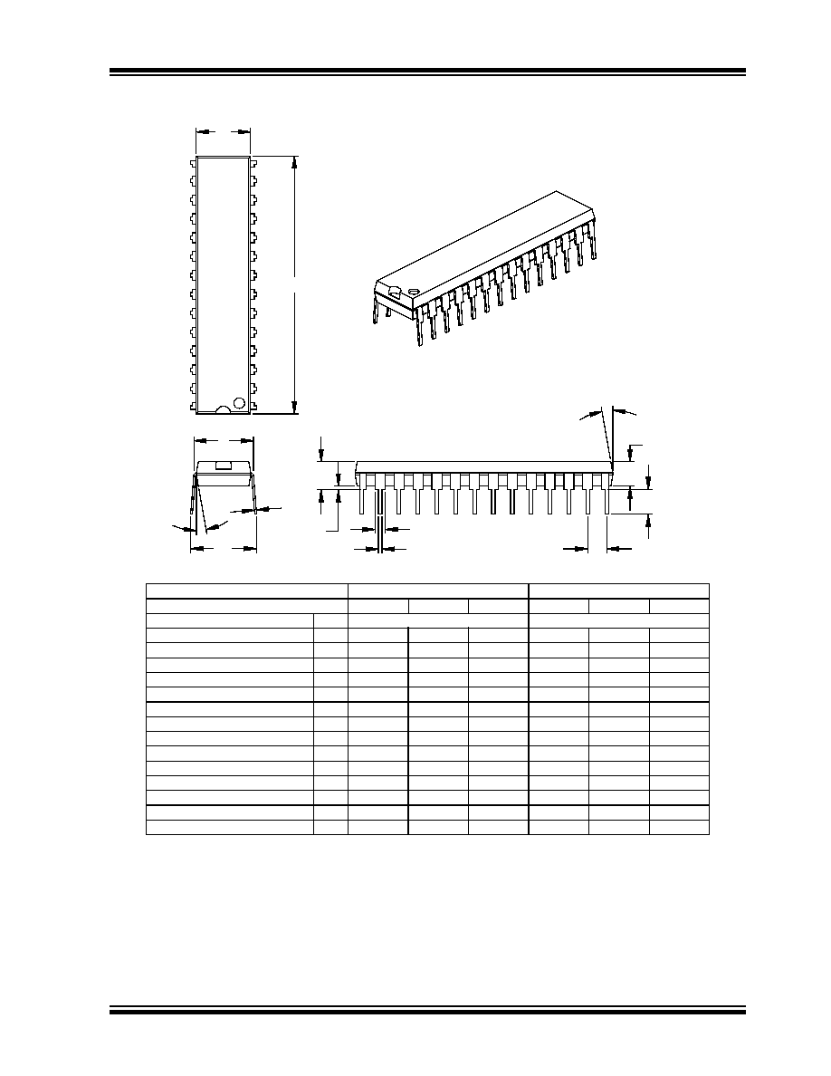
©
2006 Microchip Technology Inc.
Advance Information
DS70178A-page 259
dsPIC30F1010/202X
28-Lead Skinny Plastic Dual In-line (SP) ≠ 300 mil Body (PDIP)
15
10
5
15
10
5
Mold Draft Angle Bottom
15
10
5
15
10
5
Mold Draft Angle Top
10.92
8.89
8.13
.430
.350
.320
eB
Overall Row Spacing
ß
0.56
0.48
0.41
.022
.019
.016
B
Lower Lead Width
1.65
1.33
1.02
.065
.053
.040
B1
Upper Lead Width
0.38
0.29
0.20
.015
.012
.008
c
Lead Thickness
3.43
3.30
3.18
.135
.130
.125
L
Tip to Seating Plane
35.18
34.67
34.16
1.385
1.365
1.345
D
Overall Length
7.49
7.24
6.99
.295
.285
.275
E1
Molded Package Width
8.26
7.87
7.62
.325
.310
.300
E
Shoulder to Shoulder Width
0.38
.015
A1
Base to Seating Plane
3.43
3.30
3.18
.135
.130
.125
A2
Molded Package Thickness
4.06
3.81
3.56
.160
.150
.140
A
Top to Seating Plane
2.54
.100
p
Pitch
28
28
n
Number of Pins
MAX
NOM
MIN
MAX
NOM
MIN
Dimension Limits
MILLIMETERS
INCHES*
Units
2
1
D
n
E1
c
eB
E
p
L
A2
B
B1
A
A1
Notes:
JEDEC Equivalent: MO-095
Drawing No. C04-070
* Controlling Parameter
Dimension D and E1 do not include mold flash or protrusions. Mold flash or protrusions shall not exceed .010" (0.254mm) per side.
ß Significant Characteristic

dsPIC30F1010/202X
DS70178A-page 260
Advance Information
©
2006 Microchip Technology Inc.
28-Lead Plastic Small Outline (SO) ≠ Wide, 300 mil Body (SOIC)
Foot Angle Top
0
4
8
0
4
8
15
12
0
15
12
0
Mold Draft Angle Bottom
15
12
0
15
12
0
Mold Draft Angle Top
0.51
0.42
0.36
.020
.017
.014
B
Lead Width
0.33
0.28
0.23
.013
.011
.009
c
Lead Thickness
1.27
0.84
0.41
.050
.033
.016
L
Foot Length
0.74
0.50
0.25
.029
.020
.010
h
Chamfer Distance
18.08
17.87
17.65
.712
.704
.695
D
Overall Length
7.59
7.49
7.32
.299
.295
.288
E1
Molded Package Width
10.67
10.34
10.01
.420
.407
.394
E
Overall Width
0.30
0.20
0.10
.012
.008
.004
A1
Standoff
ß
2.39
2.31
2.24
.094
.091
.088
A2
Molded Package Thickness
2.64
2.50
2.36
.104
.099
.093
A
Overall Height
1.27
.050
p
Pitch
28
28
n
Number of Pins
MAX
NOM
MIN
MAX
NOM
MIN
Dimension Limits
MILLIMETERS
INCHES*
Units
2
1
D
p
n
B
E
E1
L
c
45
∞
h
A2
A
A1
* Controlling Parameter
Notes:
Dimensions D and E1 do not include mold flash or protrusions. Mold flash or protrusions shall not exceed .010" (0.254mm) per side.
JEDEC Equivalent: MS-013
Drawing No. C04-052
ß Significant Characteristic
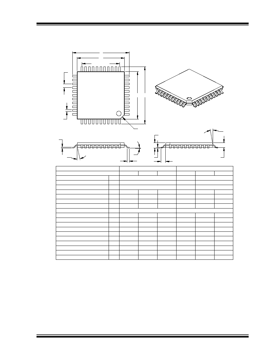
©
2006 Microchip Technology Inc.
Advance Information
DS70178A-page 261
dsPIC30F1010/202X
44-Lead Plastic Thin-Quad Flatpack (PT) 10x10x1 mm Body, 1.0/0.10 mm Lead Form (TQFP)
F
A
A1
A2
E
E1
#leads=n1
p
B
D1
D
n
1
2
c
L
CH x 45∞
1.14
0.89
0.64
.045
.035
.025
CH
Pin 1 Corner Chamfer
1.00 REF.
.039 REF.
F
Footprint (Reference)
Units
INCHES
MILLIMETERS*
Dimension Limits
MIN
NOM
MAX
MIN
NOM
MAX
Number of Pins
n
44
44
Pitch
p
.031
0.80
Overall Height
A
.039
.043
.047
1.00
1.10
1.20
Molded Package Thickness
A2
.037
.039
.041
0.95
1.00
1.05
Standoff
A1
.002
.004
.006
0.05
0.10
0.15
Foot Length
L
.018
.024
.030
0.45
0.60
0.75
Foot Angle
0
3.5
7
0
3.5
7
Overall Width
E
.463
.472
.482
11.75
12.00
12.25
Overall Length
D
.463
.472
.482
11.75
12.00
12.25
Molded Package Width
E1
.390
.394
.398
9.90
10.00
10.10
Molded Package Length
D1
.390
.394
.398
9.90
10.00
10.10
Pins per Side
n1
11
11
Lead Thickness
c
.004
.006
.008
0.09
0.15
0.20
Lead Width
B
.012
.015
.017
0.30
0.38
0.44
Mold Draft Angle Top
5
10
15
5
10
15
Mold Draft Angle Bottom
5
10
15
5
10
15
Dimensions D and E1 do not include mold flash or protrusions. Mold flash or protrusions shall not exceed .010" (0.254mm) per side.
Notes:
JEDEC Equivalent: MS-026
Revised 07-22-05
* Controlling Parameter
REF: Reference Dimension, usually without tolerance, for information purposes only.
See ASME Y14.5M
Drawing No. C04-076
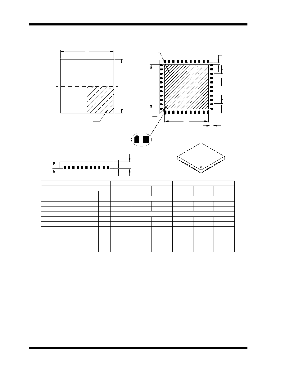
dsPIC30F1010/202X
DS70178A-page 262
Advance Information
©
2006 Microchip Technology Inc.
44-Lead Plastic Quad Flat No Lead Package (ML) 8x8 mm Body (QFN)
D2
D
TOP VIEW
n
1
L
E2
BOTTOM VIEW
B
E
2
PIN 1
INDEX ON
EXPOSED PAD
(NOTE 1)
INDEX AREA
OPTIONAL
DETAIL: CONTACT VARIANTS
(PROFILE MAY VARY)
p
A1
A
A3
EXPOSED
METAL PAD
(NOTE 2)
K
INCHES
NOM
.026 BSC
.010 REF
BSC: Basic Dimension. Theoretically exact value shown without tolerances.
REF: Reference Dimension, usually without tolerance, for information purposes only.
Number of Contacts
Overall Height
See ASME Y14.5M
See ASME Y14.5M
Contact Width
* Controlling Parameter
Overall Width
Overall Length
Contact Length
ß
Exposed Pad Width
Exposed Pad Length
JEDEC equivalent: M0-220
Base Thickness
Notes:
Pitch
Standoff
Units
Dimension Limits
A1
A
B
D
E2
D2
A3
p
.000
.309
.309
.236
.236
.014
.008
L
E
.031
MIN
n
.258
.013
.016
.315
.258
.315
.035
.001
.260
.321
.013
.019
.260
.002
.039
.321
MAX
44
0.65 BSC
0.25 REF
7.85
5.99
5.99
0.35
0.20
0.80
7.85
0
0.33
8.00
0.40
6.55
6.55
0.90
0.02
8.00
MILLIMETERS*
MIN
NOM
44
8.15
6.60
6.60
0.48
0.35
1.00
0.05
8.15
MAX
1. Pin 1 visual index feature may vary, but must be located within the hatched area.
2. Exposed pad varies according to die attach paddle size.
Contact-to-Exposed-Pad
ß
K
.014
-
-
0.20
-
-
ß Significant Characteristic
Revised 09-12-05
Drawing No. C04-103

©
2006 Microchip Technology Inc.
Advance Information
DS70178A-page 263
dsPIC30F1010/202X
THE MICROCHIP WEB SITE
Microchip provides online support via our WWW site at
www.microchip.com. This web site is used as a means
to make files and information easily available to
customers. Accessible by using your favorite Internet
browser, the web site contains the following
information:
∑ Product Support ≠ Data sheets and errata,
application notes and sample programs, design
resources, user's guides and hardware support
documents, latest software releases and archived
software
∑ General Technical Support ≠ Frequently Asked
Questions (FAQ), technical support requests,
online discussion groups, Microchip consultant
program member listing
∑ Business of Microchip ≠ Product selector and
ordering guides, latest Microchip press releases,
listing of seminars and events, listings of
Microchip sales offices, distributors and factory
representatives
CUSTOMER CHANGE NOTIFICATION
SERVICE
Microchip's customer notification service helps keep
customers current on Microchip products. Subscribers
will receive e-mail notification whenever there are
changes, updates, revisions or errata related to a
specified product family or development tool of interest.
To register, access the Microchip web site at
www.microchip.com, click on Customer Change
Notification and follow the registration instructions.
CUSTOMER SUPPORT
Users of Microchip products can receive assistance
through several channels:
∑ Distributor or Representative
∑ Local Sales Office
∑ Field Application Engineer (FAE)
∑ Technical Support
Customers should contact their distributor,
representative or field application engineer (FAE) for
support. Local sales offices are also available to help
customers. A listing of sales offices and locations is
included in the back of this document.
Technical support is available through the web site
at: http://support.microchip.com

dsPIC30F1010/202X
DS70178A-page 264
Advance Information
©
2006 Microchip Technology Inc.
READER RESPONSE
It is our intention to provide you with the best documentation possible to ensure successful use of your Microchip prod-
uct. If you wish to provide your comments on organization, clarity, subject matter, and ways in which our documentation
can better serve you, please FAX your comments to the Technical Publications Manager at (480) 792-4150.
Please list the following information, and use this outline to provide us with your comments about this document.
To:
Technical Publications Manager
RE:
Reader Response
Total Pages Sent ________
From: Name
Company
Address
City / State / ZIP / Country
Telephone: (_______) _________ - _________
Application (optional):
Would you like a reply? Y N
Device: Literature
Number:
Questions:
FAX: (______) _________ - _________
DS70178A
dsPIC30F1010/202X
1.
What are the best features of this document?
2.
How does this document meet your hardware and software development needs?
3.
Do you find the organization of this document easy to follow? If not, why?
4.
What additions to the document do you think would enhance the structure and subject?
5.
What deletions from the document could be made without affecting the overall usefulness?
6.
Is there any incorrect or misleading information (what and where)?
7.
How would you improve this document?

©
2006 Microchip Technology Inc.
Advance Information
DS70178A-page 265
dsPIC30F1010/202X
APPENDIX A:
REVISION HISTORY
Revision A (June 2006)
∑ Initial release of this document.

dsPIC30F1010/202X
DS70178A-page 266
Advance Information
©
2006 Microchip Technology Inc.
NOTES:

©
2006 Microchip Technology Inc.
Advance Information
DS70178A-page 267
dsPIC30F1010/202X
INDEX
A
A/D .................................................................................... 165
Configuring Analog Port............................................ 182
AC Characteristics ............................................................ 232
Load Conditions ........................................................ 232
AC Temperature and Voltage Specifications .................... 232
Address Generator Units .................................................... 43
Alternate Vector Table ........................................................ 53
Assembler
MPASM Assembler................................................... 222
Automatic Clock Stretch.................................................... 152
During 10-bit Addressing (STREN = 1)..................... 152
During 7-bit Addressing (STREN = 1)....................... 152
Receive Mode ........................................................... 152
Transmit Mode .......................................................... 152
B
Band Gap Start-up Time
Requirements............................................................ 239
Timing Characteristics .............................................. 239
Barrel Shifter ....................................................................... 29
Baud Rate Error Calculation (BRGH = 0) ......................... 158
Bit-Reversed Addressing .................................................... 47
Example ...................................................................... 47
Implementation ........................................................... 47
Modifier Values (table) ................................................ 48
Sequence Table (16-Entry)......................................... 48
Block Diagrams
16-bit Timer1 Module .................................................. 88
DSP Engine ................................................................ 26
dsPIC30F2020 ............................................................ 10
dsPIC30F2023 ............................................................ 16
External Power-on Reset Circuit............................... 207
I
2
C............................................................................. 150
Input Capture Mode .................................................... 97
Oscillator System ...................................................... 199
Output Compare Mode ............................................. 101
Reset System............................................................ 205
Shared Port Structure ................................................. 77
SPI ............................................................................ 146
SPI Master/Slave Connection ................................... 146
UART ........................................................................ 157
Brown-out Reset
Timing Requirements................................................ 238
C
C Compilers
MPLAB C18 .............................................................. 222
MPLAB C30 .............................................................. 222
CLKOUT and I/O Timing
Characteristics .......................................................... 236
Requirements............................................................ 236
Code Examples
Erasing a Row of Program Memory............................ 83
Initiating a Programming Sequence ............................ 84
Loading Write Latches ................................................ 84
Code Protection ................................................................ 191
Configuring Analog Port Pins .............................................. 78
Control Registers ................................................................ 82
NVMADR .................................................................... 82
NVMADRU.................................................................. 82
NVMCON .................................................................... 82
NVMKEY..................................................................... 82
Core Architecture
Overview..................................................................... 21
Core Register Map.............................................................. 39
Customer Change Notification Service............................. 263
Customer Notification Service .......................................... 263
Customer Support............................................................. 263
D
Data Access from Program Memory Using
Program Space Visibility............................................. 34
Data Accumulators and Adder/Subtractor .......................... 27
Data Space Write Saturation ...................................... 29
Overflow and Saturation ............................................. 27
Round Logic ............................................................... 28
Write Back .................................................................. 28
Data Address Space........................................................... 35
Alignment.................................................................... 38
Alignment (Figure) ...................................................... 38
MCU and DSP (MAC Class) Instructions ................... 37
Memory Map......................................................... 35, 36
Near Data Space ........................................................ 39
Software Stack ........................................................... 39
Spaces........................................................................ 38
Width .......................................................................... 38
DC Characteristics
I/O Pin Input Specifications ...................................... 228
I/O Pin Output Specifications.................................... 231
Idle Current (I
IDLE
) .................................................... 228
Operating Current (I
DD
) ............................................ 227
Power-Down Current (I
PD
)........................................ 229
Program and EEPROM ............................................ 231
Development Support ....................................................... 221
Device Configuration
Register Map ............................................................ 212
Device Configuration Registers ........................................ 210
FGS .......................................................................... 210
FOSC........................................................................ 210
FWDT ....................................................................... 210
Device Overview................................................................... 9
Divide Support .................................................................... 24
DSP Engine ........................................................................ 25
Multiplier ..................................................................... 27
dsPIC30F2020 Block Diagram ........................................... 13
Dual Output Compare Match Mode .................................. 102
Continuous Pulse Mode ........................................... 102
Single Pulse Mode.................................................... 102
E
Electrical Characteristics .................................................. 225
AC............................................................................. 232
Equations
I
2
C ............................................................................ 154
UART Baud Rate with BRGH = 0 ............................. 158
UART Baud Rate with BRGH = 1 ............................. 158
Errata .................................................................................... 8
External Clock Input.......................................................... 201
External Clock Timing Characteristics
Type A, B and C Timer ............................................. 240
External Clock Timing Requirements ............................... 233
Type A Timer ............................................................ 240
Type B Timer ............................................................ 241
Type C Timer............................................................ 241
External Interrupt Requests ................................................ 53

dsPIC30F1010/202X
DS70178A-page 268
Advance Information
©
2006 Microchip Technology Inc.
F
Fast Context Saving............................................................ 53
Firmware Instructions........................................................ 213
Flash Program Memory....................................................... 81
In-Circuit Serial Programming (ICSP) ......................... 81
Run Time Self-Programming (RTSP) ......................... 81
Table Instruction Operation Summary ........................ 81
I
I/O Pin Specifications
Input .......................................................................... 228
Output ....................................................................... 231
I/O Ports .............................................................................. 77
Parallel I/O (PIO)......................................................... 77
I
2
C ..................................................................................... 149
I
2
C 10-bit Slave Mode Operation ...................................... 151
Reception .................................................................. 151
Transmission............................................................. 151
I
2
C 7-bit Slave Mode Operation ........................................ 151
Reception .................................................................. 151
Transmission............................................................. 151
I
2
C Master Mode
Baud Rate Generator ................................................ 154
Clock Arbitration........................................................ 154
Multi-Master Communication, Bus Collision and
Bus Arbitration .................................................. 154
Reception .................................................................. 153
Transmission............................................................. 153
I
2
C Module
Addresses ................................................................. 151
Bus Data Timing Characteristics
Master Mode ..................................................... 250
Slave Mode ....................................................... 252
Bus Data Timing Requirements
Master Mode ..................................................... 251
Slave Mode ....................................................... 253
Bus Start/Stop Bits Timing Characteristics
Master Mode ..................................................... 250
Slave Mode ....................................................... 252
General Call Address Support .................................. 153
Interrupts ................................................................... 152
IPMI Support ............................................................. 153
Master Operation ...................................................... 153
Master Support ......................................................... 153
Operating Function Description ................................ 149
Operation During CPU Sleep and Idle Modes .......... 154
Pin Configuration ...................................................... 149
Programmer's Model................................................. 149
Register Map............................................................. 155
Registers ................................................................... 149
Slope Control ............................................................ 153
Software Controlled Clock Stretching (STREN = 1).. 152
Various Modes .......................................................... 149
Idle Current (I
IDLE
)............................................................. 228
In-Circuit Debugger ........................................................... 211
In-Circuit Serial Programming (ICSP) ............................... 191
Initialization Condition for RCON Register Case 1............ 208
Initialization Condition for RCON Register Case 2............ 208
Input Capture (CAPX) Timing Characteristics................... 242
Input Capture Interrupts ...................................................... 99
Register Map............................................................. 100
Input Capture Module.......................................................... 97
Simple Capture Event Mode ....................................... 98
Sleep and Idle Modes ................................................. 99
Input Capture Timing Requirements ................................. 242
Input Change Notification.................................................... 78
Input Change Notification Register Map ............................. 80
Instruction Addressing Modes ............................................ 43
File Register Instructions ............................................ 43
Fundamental Modes Supported ................................. 43
MAC Instructions ........................................................ 44
MCU Instructions ........................................................ 44
Move and Accumulator Instructions............................ 44
Other Instructions ....................................................... 44
Instruction Set................................................................... 213
Instruction Set Overview ................................................... 216
Inter-Integrated Circuit. See I
2
C
Internal Clock Timing Examples ....................................... 234
Internet Address ............................................................... 263
Interrupt Priority .................................................................. 50
Interrupt Sequence ............................................................. 53
Interrupt Stack Frame ................................................. 53
Interrupts............................................................................. 49
Traps .......................................................................... 51
L
Load Conditions................................................................ 232
M
Memory Organization ......................................................... 31
Microchip Internet Web Site.............................................. 263
Modulo Addressing ............................................................. 45
Applicability................................................................. 47
Operation Example ..................................................... 46
Start and End Address ............................................... 45
W Address Register Selection .................................... 45
Motor Control PWM Module
Fault Timing Characteristics ..................................... 244
Timing Characteristics .............................................. 244
Timing Requirements................................................ 244
MPLAB ASM30 Assembler, Linker, Librarian ................... 222
MPLAB ICD 2 In-Circuit Debugger ................................... 223
MPLAB ICE 2000 High-Performance Universal
In-Circuit Emulator ............................................................ 223
MPLAB ICE 4000 High-Performance Universal
In-Circuit Emulator .................................................... 223
MPLAB Integrated Development Environment Software .. 221
MPLAB PM3 Device Programmer .................................... 223
MPLINK Object Linker/MPLIB Object Librarian ................ 222
O
OC/PWM Module Timing Characteristics ......................... 243
Operating Current (I
DD
) .................................................... 227
Oscillator
Operating Modes (Table).......................................... 198
System Overview...................................................... 191
Oscillator Configurations................................................... 200
Fail-Safe Clock Monitor ............................................ 202
Initial Clock Source Selection ................................... 200
Phase Locked Loop (PLL) ........................................ 200
Start-up Timer (OST) ................................................ 200
Oscillator Selection ........................................................... 191
Oscillator Start-up Timer
Timing Characteristics .............................................. 237
Timing Requirements................................................ 238
Output Compare Interrupts ............................................... 104
Output Compare Mode
Register Map ............................................................ 105
Output Compare Module .................................................. 101
Timing Characteristics .............................................. 242
Timing Requirements................................................ 242
Output Compare Operation During CPU Idle Mode ......... 103
Output Compare Sleep Mode Operation .......................... 103

©
2006 Microchip Technology Inc.
Advance Information
DS70178A-page 269
dsPIC30F1010/202X
P
Packaging Information
Marking ..................................................................... 257
PICSTART Plus Development Programmer ..................... 224
Pinout Descriptions ................................................. 11, 14, 17
PLL Clock Timing Specifications....................................... 234
POR. See Power-on Reset
Port Register Map
dsPIC30F2020 ............................................................ 79
dsPIC30F2023 ............................................................ 80
Port Write/Read Example ................................................... 78
Power-Down Current (I
PD
) ................................................ 229
Power-on Reset (POR) ..................................................... 191
Oscillator Start-up Timer (OST) ................................ 191
Power-up Timer (PWRT) .......................................... 191
Power-Saving Modes ........................................................ 209
Idle ............................................................................ 210
Sleep......................................................................... 209
Power-Saving Modes (Sleep and Idle) ............................. 191
Power-up Timer
Timing Characteristics .............................................. 237
Timing Requirements................................................ 238
Product Identification System ........................................... 271
Program Address Space ..................................................... 31
Construction................................................................ 32
Data Access from Program Memory Using Table
Instructions ......................................................... 33
Data Access from, Address Generation...................... 32
Memory Map ............................................................... 31
Table Instructions
TBLRDH ............................................................. 33
TBLRDL .............................................................. 33
TBLWTH ............................................................. 33
TBLWTL.............................................................. 33
Program and EEPROM Characteristics ............................ 231
Program Counter ................................................................ 22
Program Data Table Access ............................................... 34
Program Space Visibility
Window into Program Space Operation...................... 35
Programmer's Model........................................................... 22
Diagram ...................................................................... 23
Programming Operations .................................................... 83
Algorithm for Program Flash ....................................... 83
Erasing a Row of Program Memory............................ 83
Initiating the Programming Sequence......................... 84
Loading Write Latches ................................................ 84
Programming, Device Instructions .................................... 213
R
Reader Response ............................................................. 264
Reset......................................................................... 191, 204
Reset Sequence ................................................................. 51
Reset Sources ............................................................ 51
Reset Timing Characteristics ............................................ 237
Reset Timing Requirements ............................................. 238
Resets
POR .......................................................................... 206
POR with Long Crystal Start-up Time....................... 207
POR, Operating without FSCM and PWRT .............. 207
RTSP Operation.................................................................. 82
S
Sales and Support ............................................................ 271
Serial Peripheral Interface. See SPI
Simple Capture Event Mode
Capture Buffer Operation ........................................... 98
Capture Prescaler....................................................... 98
Hall Sensor Mode ....................................................... 98
Input Capture in CPU Idle Mode................................. 99
Timer2 and Timer3 Selection Mode ........................... 98
Simple OC/PWM Mode Timing Requirements ................. 243
Simple Output Compare Match Mode .............................. 102
Simple PWM Mode ........................................................... 102
Period ....................................................................... 103
Software Simulator (MPLAB SIM) .................................... 222
Software Stack Pointer, Frame Pointer .............................. 22
CALL Stack Frame ..................................................... 39
SPI .................................................................................... 145
SPI Mode
Slave Select Synchronization ................................... 147
SPI1 Register Map ................................................... 148
SPI Module ....................................................................... 145
Framed SPI Support................................................. 146
Operating Function Description ................................ 145
SDOx Disable ........................................................... 145
Timing Characteristics
Master Mode (CKE = 0).................................... 245
Master Mode (CKE = 1).................................... 246
Slave Mode (CKE = 1).............................. 247, 248
Timing Requirements
Master Mode (CKE = 0).................................... 245
Master Mode (CKE = 1).................................... 246
Slave Mode (CKE = 0)...................................... 247
Slave Mode (CKE = 1)...................................... 249
Word and Byte Communication ................................ 145
SPI Operation During CPU Idle Mode .............................. 147
SPI Operation During CPU Sleep Mode........................... 147
STATUS Register ............................................................... 22
Symbols used in Opcode Descriptions ............................. 214
System Integration............................................................ 191
Register Map ............................................................ 212
T
Temperature and Voltage Specifications
AC............................................................................. 232
Timer1 Module.................................................................... 87
16-bit Asynchronous Counter Mode ........................... 87
16-bit Synchronous Counter Mode............................. 87
16-bit Timer Mode ...................................................... 87
Gate Operation ........................................................... 88
Interrupt ...................................................................... 89
Operation During Sleep Mode .................................... 88
Prescaler .................................................................... 88
Register Map .............................................................. 90
Timer2 and Timer3 Selection Mode.................................. 102
Timer2/3 Module................................................................. 91
16-bit Timer Mode ...................................................... 91
32-bit Synchronous Counter Mode............................. 91
32-bit Timer Mode ...................................................... 91
ADC Event Trigger ..................................................... 94
Gate Operation ........................................................... 94
Interrupt ...................................................................... 94
Operation During Sleep Mode .................................... 94
Register Map .............................................................. 95
Timer Prescaler .......................................................... 94

dsPIC30F1010/202X
DS70178A-page 270
Advance Information
©
2006 Microchip Technology Inc.
Timing Characteristics
A/D Conversion
10-Bit High-speed (CHPS = 01,
SIMSAM = 0, ASAM = 0, SSRC = 000) .... 255
Band Gap Start-up Time ........................................... 239
CLKOUT and I/O....................................................... 236
External Clock ........................................................... 232
I
2
C Bus Data
Master Mode ..................................................... 250
Slave Mode ....................................................... 252
I
2
C Bus Start/Stop Bits
Master Mode ..................................................... 250
Slave Mode ....................................................... 252
Input Capture (CAPX) ............................................... 242
Motor Control PWM Module...................................... 244
Motor Control PWM Module Falult ............................ 244
OC/PWM Module ...................................................... 243
Oscillator Start-up Timer ........................................... 237
Output Compare Module........................................... 242
Power-up Timer ........................................................ 237
Reset......................................................................... 237
SPI Module
Master Mode (CKE = 0) .................................... 245
Master Mode (CKE = 1) .................................... 246
Slave Mode (CKE = 0) ...................................... 247
Slave Mode (CKE = 1) ...................................... 248
Type A, B and C Timer External Clock ..................... 240
Watchdog Timer........................................................ 237
Timing Diagrams
PWM Output ............................................................. 104
Time-out Sequence on Power-up (MCLR Not
Tied to V
DD
), Case 1......................................... 206
Time-out Sequence on Power-up (MCLR Not
Tied to V
DD
), Case 2......................................... 207
Time-out Sequence on Power-up (MCLR Tied
to V
DD
) .............................................................. 206
Timing Diagrams and Specifications
DC Characteristics - Internal RC Accuracy ............... 234
Timing Diagrams.See Timing Characteristics
Timing Requirements
Band Gap Start-up Time ........................................... 239
Brown-out Reset ....................................................... 238
CLKOUT and I/O....................................................... 236
External Clock ........................................................... 233
I
2
C Bus Data (Master Mode)..................................... 251
I
2
C Bus Data (Slave Mode)....................................... 253
Input Capture ............................................................ 242
Motor Control PWM Module...................................... 244
Oscillator Start-up Timer ........................................... 238
Output Compare Module........................................... 242
Power-up Timer ........................................................ 238
Reset......................................................................... 238
Simple OC/PWM Mode ............................................. 243
SPI Module
Master Mode (CKE = 0) .................................... 245
Master Mode (CKE = 1) .................................... 246
Slave Mode (CKE = 0) ...................................... 247
Slave Mode (CKE = 1) ...................................... 249
Type A Timer External Clock .................................... 240
Type B Timer External Clock .................................... 241
Type C Timer External Clock .................................... 241
Watchdog Timer........................................................ 238
Timing Specifications
PLL Clock.................................................................. 234
Traps
Trap Sources .............................................................. 51
U
UART
Baud Rate Generator (BRG) .................................... 158
Enabling and Setting Up UART ................................ 158
IrDA
Built-in Encoder and Decoder........................... 159
Receiving
8-bit or 9-bit Data Mode .................................... 159
Transmitting
8-bit Data Mode ................................................ 159
9-bit Data Mode ................................................ 159
Break and Sync Sequence ............................... 159
UART Module
UART1 Register Map................................................ 164
Unit ID Locations .............................................................. 191
Universal Asynchronous Receiver Transmitter. See UART
W
Wake-up from Sleep ......................................................... 191
Wake-up from Sleep and Idle ............................................. 53
Watchdog Timer
Timing Characteristics .............................................. 237
Timing Requirements................................................ 238
Watchdog Timer (WDT)............................................ 191, 209
Enabling and Disabling ............................................. 209
Operation .................................................................. 209
WWW Address ................................................................. 263
WWW, On-Line Support ....................................................... 8
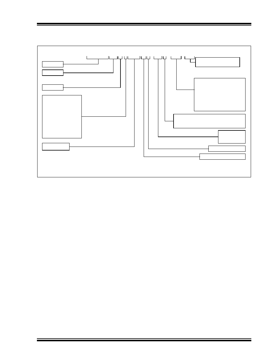
©
2006 Microchip Technology Inc.
Advance Information
DS70178A-page 271
dsPIC30F1010/202X
PRODUCT IDENTIFICATION SYSTEM
To order or obtain information, e.g., on pricing or delivery, refer to the factory or the listed sales office.
d s P I C 3 0 F 2 0 2 0 AT - 3 0 E / S O - E S
Example:
dsPIC30F2020AT-301/SO = 30 MIPS, Industrial temp., SOIC package, Rev. A
Trademark
Architecture
Flash
E = Extended High Temp -40∞C to +125∞C
I = Industrial -40∞C to +85∞C
Temperature
Device ID
Package
MM = QFN
PT = TQFP
SP = SPDIP
SO = SOIC
S
= Die (Waffle Pack)
W
= Die (Wafers)
Memory Size in Bytes
0 = ROMless
1 = 1K to 6K
2 = 7K to 12K
3 = 13K to 24K
4 = 25K to 48K
5 = 49K to 96K
6 = 97K to 192K
7 = 193K to 384K
8 = 385K to 768K
9 = 769K and Up
Custom ID (3 digits) or
T = Tape and Reel
A,B,C... = Revision Level
Engineering Sample (ES)
Speed
20 = 20 MIPS
30 = 30 MIPS

DS70178A-page 272
Advance Information
©
2006 Microchip Technology Inc.
AMERICAS
Corporate Office
2355 West Chandler Blvd.
Chandler, AZ 85224-6199
Tel: 480-792-7200
Fax: 480-792-7277
Technical Support:
http://support.microchip.com
Web Address:
www.microchip.com
Asia Pacific Office
Suites 3707-14, 37th Floor
Tower 6, The Gateway
Habour City, Kowloon
Hong Kong
Tel: 852-2401-1200
Fax: 852-2401-3431
Atlanta
Alpharetta, GA
Tel: 770-640-0034
Fax: 770-640-0307
Boston
Westborough, MA
Tel: 774-760-0087
Fax: 774-760-0088
Chicago
Itasca, IL
Tel: 630-285-0071
Fax: 630-285-0075
Dallas
Addison, TX
Tel: 972-818-7423
Fax: 972-818-2924
Detroit
Farmington Hills, MI
Tel: 248-538-2250
Fax: 248-538-2260
Kokomo
Kokomo, IN
Tel: 765-864-8360
Fax: 765-864-8387
Los Angeles
Mission Viejo, CA
Tel: 949-462-9523
Fax: 949-462-9608
San Jose
Mountain View, CA
Tel: 650-215-1444
Fax: 650-961-0286
Toronto
Mississauga, Ontario,
Canada
Tel: 905-673-0699
Fax: 905-673-6509
ASIA/PACIFIC
Australia - Sydney
Tel: 61-2-9868-6733
Fax: 61-2-9868-6755
China - Beijing
Tel: 86-10-8528-2100
Fax: 86-10-8528-2104
China - Chengdu
Tel: 86-28-8676-6200
Fax: 86-28-8676-6599
China - Fuzhou
Tel: 86-591-8750-3506
Fax: 86-591-8750-3521
China - Hong Kong SAR
Tel: 852-2401-1200
Fax: 852-2401-3431
China - Qingdao
Tel: 86-532-8502-7355
Fax: 86-532-8502-7205
China - Shanghai
Tel: 86-21-5407-5533
Fax: 86-21-5407-5066
China - Shenyang
Tel: 86-24-2334-2829
Fax: 86-24-2334-2393
China - Shenzhen
Tel: 86-755-8203-2660
Fax: 86-755-8203-1760
China - Shunde
Tel: 86-757-2839-5507
Fax: 86-757-2839-5571
China - Wuhan
Tel: 86-27-5980-5300
Fax: 86-27-5980-5118
China - Xian
Tel: 86-29-8833-7250
Fax: 86-29-8833-7256
ASIA/PACIFIC
India - Bangalore
Tel: 91-80-4182-8400
Fax: 91-80-4182-8422
India - New Delhi
Tel: 91-11-5160-8631
Fax: 91-11-5160-8632
India - Pune
Tel: 91-20-2566-1512
Fax: 91-20-2566-1513
Japan - Yokohama
Tel: 81-45-471- 6166
Fax: 81-45-471-6122
Korea - Gumi
Tel: 82-54-473-4301
Fax: 82-54-473-4302
Korea - Seoul
Tel: 82-2-554-7200
Fax: 82-2-558-5932 or
82-2-558-5934
Malaysia - Penang
Tel: 60-4-646-8870
Fax: 60-4-646-5086
Philippines - Manila
Tel: 63-2-634-9065
Fax: 63-2-634-9069
Singapore
Tel: 65-6334-8870
Fax: 65-6334-8850
Taiwan - Hsin Chu
Tel: 886-3-572-9526
Fax: 886-3-572-6459
Taiwan - Kaohsiung
Tel: 886-7-536-4818
Fax: 886-7-536-4803
Taiwan - Taipei
Tel: 886-2-2500-6610
Fax: 886-2-2508-0102
Thailand - Bangkok
Tel: 66-2-694-1351
Fax: 66-2-694-1350
EUROPE
Austria - Wels
Tel: 43-7242-2244-3910
Fax: 43-7242-2244-393
Denmark - Copenhagen
Tel: 45-4450-2828
Fax: 45-4485-2829
France - Paris
Tel: 33-1-69-53-63-20
Fax: 33-1-69-30-90-79
Germany - Munich
Tel: 49-89-627-144-0
Fax: 49-89-627-144-44
Italy - Milan
Tel: 39-0331-742611
Fax: 39-0331-466781
Netherlands - Drunen
Tel: 31-416-690399
Fax: 31-416-690340
Spain - Madrid
Tel: 34-91-708-08-90
Fax: 34-91-708-08-91
UK - Wokingham
Tel: 44-118-921-5869
Fax: 44-118-921-5820
W
ORLDWIDE
S
ALES
AND
S
ERVICE
06/08/06