
2003 Microchip Technology Inc.
DS11195C-page 1
M
MCP41XXX/42XXX
Features
� 256 taps for each potentiometer
� Potentiometer values for 10 k
, 50 k and
100 k
� Single and dual versions
� SPITM serial interface (mode 0,0 and 1,1)
� �1 LSB max INL & DNL
� Low power CMOS technology
� 1 �A maximum supply current in static operation
� Multiple devices can be daisy-chained together
(MCP42XXX only)
� Shutdown feature open circuits of all resistors for
maximum power savings
� Hardware shutdown pin available on MCP42XXX
only
� Single supply operation (2.7V - 5.5V)
� Industrial temperature range: -40�C to +85�C
� Extended temperature range: -40�C to +125�C
Block Diagram
Description
The MCP41XXX and MCP42XXX devices are 256-
position, digital potentiometers available in 10 k
,
50 k
and 100 k resistance versions. The
MCP41XXX is a single-channel device and is offered in
an 8-pin PDIP or SOIC package. The MCP42XXX con-
tains two independent channels in a 14-pin PDIP, SOIC
or TSSOP package. The wiper position of the
MCP41XXX/42XXX varies linearly and is controlled via
an industry-standard SPI interface. The devices con-
sume <1 �A during static operation. A software shut-
down feature is provided that disconnects the "A"
terminal from the resistor stack and simultaneously con-
nects the wiper to the "B" terminal. In addition, the dual
MCP42XXX has a SHDN pin that performs the same
function in hardware. During shutdown mode, the con-
tents of the wiper register can be changed and the
potentiometer returns from shutdown to the new value.
The wiper is reset to the mid-scale position (80h) upon
power-up. The RS (reset) pin implements a hardware
reset and also returns the wiper to mid-scale. The
MCP42XXX SPI interface includes both the SI and SO
pins, allowing daisy-chaining of multiple devices. Chan-
nel-to-channel resistance matching on the MCP42XXX
varies by less than 1%. These devices operate from a
single 2.7 - 5.5V supply and are specified over the
extended and industrial temperature ranges.
Package Types
16-Bit
Shift
V
DD
V
SS
SI
SCK
RS SHDN
PB1
PA1
PW1
Resistor
Array 1*
Wiper
Register
PB0
PW0
PA0
Resistor
Array 0
Wiper
Register
Register
S0
Control
Logic
CS
*Potentiometer P1 is only available on the dual
MCP42XXX version.
MCP42XXX
1
2
3
4
11
12
13
14
8
9
10
5
6
7
PDIP/SOIC/TSSOP
PB1
PA1
PW1
SHDN
SO
RS
PW0
PB0
CS
PA0
SCK
SI
V
SS
V
DD
M
C
P
4
1XXX
1
2
3
4
5
6
7
8
PDIP/SOIC
PB0
PA0
V
DD
PW0
V
SS
CS
SCK
SI
Single/Dual Digital Potentiometer with SPI
TM
Interface
MCP41XXX/42XXX
DS11195C-page 2
2003 Microchip Technology Inc.
1.0
ELECTRICAL CHARACTERISTICS
DC CHARACTERISTICS: 10 k
VERSION
Electrical Characteristics: Unless otherwise indicated, V
DD
= +2.7V to 5.5V, T
A
= -40�C to +85�C (TSSOP devices are only specified at +25�C and
+85�C). Typical specifications represent values for V
DD
= 5V, V
SS
= 0V, V
B
= 0V, T
A
= +25�C.
Parameters
Sym
Min
Typ
Max
Units
Conditions
Rheostat Mode
Nominal Resistance
R
8
10
12
k
T
A
= +25�C (Note 1)
Rheostat Differential Non Linearity
R-DNL
-1
�1/4
+1
LSB
Note 2
Rheostat Integral Non Linearity
R-INL
-1
�1/4
+1
LSB
Note 2
Rheostat Tempco
R
AB
/
T
--
800
--
ppm/�C
Wiper Resistance
R
W
--
52
100
V
DD
= 5.5V, I
W
= 1 mA, code 00h
R
W
--
73
125
V
DD
= 2.7V, I
W
= 1 mA, code 00h
Wiper Current
I
W
-1
--
+1
mA
Nominal Resistance Match
R/R
--
0.2
1
%
MCP42010 only, P0 to P1; T
A
= +25�C
Potentiometer Divider
Resolution
N
8
--
--
Bits
Monotonicity
N
8
--
--
Bits
Differential Non-Linearity
DNL
-1
�1/4
+1
LSB
Note 3
Integral Non-Linearity
INL
-1
�1/4
+1
LSB
Note 3
Voltage Divider Tempco
V
W
/
T
--
1
--
ppm/�C Code 80h
Full Scale Error
V
WFSE
-2
-0.7
0
LSB
Code FFh, V
DD
= 5V, see Figure 2-25
V
WFSE
-2
-0.7
0
LSB
Code FFh, V
DD
= 3V, see Figure 2-25
Zero Scale Error
V
WZSE
0
+0.7
+2
LSB
Code 00h, V
DD
= 5V, see Figure 2-25
V
WZSE
0
+0.7
+2
LSB
Code 00h, V
DD
= 3V, see Figure 2-25
Resistor Terminals
Voltage Range
V
A,B,W
0
--
V
DD
Note 4
Capacitance (C
A
or C
B
)
--
15
--
pF
f = 1 MHz, Code = 80h, see Figure 2-30
Capacitance
C
W
--
5.6
--
pF
f = 1 MHz, Code = 80h, see Figure 2-30
Dynamic Characteristics (All dynamic characteristics use V
DD
= 5V)
Bandwidth -3dB
BW
--
1
--
MHz
V
B
= 0V, Measured at Code 80h,
Output Load = 30
P
F
Settling Time
t
S
--
2
--
�S
V
A
= V
DD
,V
B
= 0V, �1% Error Band, Transition
from Code 00h to Code 80h, Output Load = 30 pF
Resistor Noise Voltage
e
NWB
--
9
--
nV/
Hz V
A
= Open, Code 80h
, f =1 kHz
Crosstalk
C
T
--
-95
--
dB
V
A
= V
DD
, V
B
= 0V (Note 5)
Digital Inputs/Outputs (CS, SCK, SI, SO) See Figure 2-12 for RS and SHDN pin operation
Schmitt Trigger High-Level Input Voltage
V
IH
0.7V
DD
--
--
V
Schmitt Trigger Low-Level Input Voltage
V
IL
--
--
0.3V
DD
V
Hysteresis of Schmitt Trigger Inputs
V
HYS
--
0.05V
DD
--
Low-Level Output Voltage
V
OL
--
--
0.40
V
I
OL
= 2.1 mA, V
DD
= 5V
High-Level Output Voltage
V
OH
V
DD
- 0.5
--
--
V
I
OH
= -400 �A, V
DD
= 5V
Input Leakage Current
I
LI
-1
--
+1
�A
CS = V
DD
, V
IN
= V
SS
or V
DD
, includes V
A
SHDN=0
Pin Capacitance (All inputs/outputs)
C
IN
, C
OUT
--
10
--
pF
V
DD
= 5.0V, T
A
= +25�C, f
c
= 1 MHz
Power Requirements
Operating Voltage Range
V
DD
2.7
--
5.5
V
Supply Current, Active
I
DDA
--
340
500
�A
V
DD
= 5.5V, CS = V
SS
, f
SCK
= 10 MHz,
SO = Open, Code FFh (Note 6)
Supply Current, Static
I
DDS
--
0.01
1
�A
CS, SHDN, RS = V
DD
= 5.5V, SO = Open (Note 6)
Power Supply Sensitivity
PSS
--
0.0015
0.0035
%/%
V
DD
= 4.5V - 5.5V, V
A
= 4.5V, Code 80h
PSS
--
0.0015
0.0035
%/%
V
DD
= 2.7V - 3.3V, V
A
= 2.7V, Code 80h
Note
1:
V
AB
= V
DD
, no connection on wiper.
2:
Rheostat position non-linearity R-INL is the deviation from an ideal value measured between the maximum resistance and the minimum
resistance wiper positions. R-DNL measures the relative step change from the ideal between successive tap positions. I
W
= 50 �A for
V
DD
= 3V and I
W
= 400 �A for V
DD
= 5V for 10 k
version. See Figure 2-26 for test circuit.
3:
INL and DNL are measured at V
W
with the device configured in the voltage divider or potentiometer mode. V
A
= V
DD
and V
B
= 0V. DNL
specification limits of �1 LSB max are specified monotonic operating conditions. See Figure 2-25 for test circuit.
4:
Resistor terminals A,B and W have no restrictions on polarity with respect to each other. Full-scale and zero-scale error were measured
using Figure 2-25.
5:
Measured at V
W
pin where the voltage on the adjacent V
W
pin is swinging full-scale.
6:
Supply current is independent of current through the potentiometers.

2003 Microchip Technology Inc.
DS11195C-page 3
MCP41XXX/42XXX
DC CHARACTERISTICS: 50 k
VERSION
Electrical Characteristics: Unless otherwise indicated, V
DD
= +2.7V to 5.5V, T
A
= -40�C to +85�C (TSSOP devices are only specified at +25�C and
+85�C). Typical specifications represent values for V
DD
= 5V, V
SS
= 0V, V
B
= 0V, T
A
= +25�C.
Parameters
Sym
Min
Typ
Max
Units
Conditions
Rheostat Mode
Nominal Resistance
R
35
50
65
k
T
A
= +25�C (Note 1)
Rheostat Differential Non-Linearity
R-DNL
-1
�1/4
+1
LSB
Note 2
Rheostat Integral Non-Linearity
R-INL
-1
�1/4
+1
LSB
Note 2
Rheostat Tempco
R
AB
/
T
--
800
--
ppm/�C
Wiper Resistance
R
W
--
125
175
V
DD
= 5.5V, I
W
= 1 mA, code 00h
R
W
--
175
250
V
DD
= 2.7V, I
W
= 1 mA, code 00h
Wiper Current
I
W
-1
--
+1
mA
Nominal Resistance Match
R/R
--
0.2
1
%
MCP42050 only, P0 to P1;T
A
= +25�C
Potentiometer Divider
Resolution
N
8
--
--
Bits
Monotonicity
N
8
--
--
Bits
Differential Non-Linearity
DNL
-1
�1/4
+1
LSB
Note 3
Integral Non-Linearity
INL
-1
�1/4
+1
LSB
Note 3
Voltage Divider Tempco
V
W
/
T
--
1
--
ppm/�C Code 80h
Full-Scale Error
V
WFSE
-1
-0.25
0
LSB
Code FFh, V
DD
= 5V, see Figure 2-25
V
WFSE
-1
-0.35
0
LSB
Code FFh, V
DD
= 3V, see Figure 2-25
Zero-Scale Error
V
WZSE
0
+0.25
+1
LSB
Code 00h, V
DD
= 5V, see Figure 2-25
V
WZSE
0
+0.35
+1
LSB
Code 00h, V
DD
= 3V, see Figure 2-25
Resistor Terminals
Voltage Range
V
A,B,W
0
--
V
DD
Note 4
Capacitance (C
A
or C
B
)
--
11
--
pF
f =1 MHz, Code = 80h, see Figure 2-30
Capacitance
C
W
--
5.6
--
pF
f =1 MHz, Code = 80h, see Figure 2-30
Dynamic Characteristics (All dynamic characteristics use V
DD
= 5V)
Bandwidth -3dB
BW
--
280
--
MHz
V
B
= 0V, Measured at Code 80h,
Output Load = 30
P
F
Settling Time
t
S
--
8
--
�S
V
A
= V
DD
,V
B
= 0V, �1% Error Band, Transition
from Code 00h to Code 80h, Output Load = 30 pF
Resistor Noise Voltage
e
NWB
--
20
--
nV/
Hz V
A
= Open, Code 80h
, f =1 kHz
Crosstalk
C
T
--
-95
--
dB
V
A
= V
DD
, V
B
= 0V (Note 5)
Digital Inputs/Outputs (CS, SCK, SI, SO) See Figure 2-12 for RS and SHDN pin operation.
Schmitt Trigger High-Level Input Voltage
V
IH
0.7V
DD
--
--
V
Schmitt Trigger Low-Level Input Voltage
V
IL
--
--
0.3V
DD
V
Hysteresis of Schmitt Trigger Inputs
V
HYS
--
0.05V
DD
--
Low-Level Output Voltage
V
OL
--
--
0.40
V
I
OL
= 2.1 mA, V
DD
= 5V
High-Level Output Voltage
V
OH
V
DD
- 0.5
--
--
V
I
OH
= -400 �A, V
DD
= 5V
Input Leakage Current
I
LI
-1
--
+1
�A
CS = V
DD
, V
IN
= V
SS
or V
DD
, includes V
A
SHDN=0
Pin Capacitance (All inputs/outputs)
C
IN
, C
OUT
--
10
--
pF
V
DD
= 5.0V, T
A
= +25�C, f
c
= 1 MHz
Power Requirements
Operating Voltage Range
V
DD
2.7
--
5.5
V
Supply Current, Active
I
DDA
--
340
500
�A
V
DD
= 5.5V, CS = V
SS
, f
SCK
= 10 MHz,
SO = Open, Code FFh (Note 6)
Supply Current, Static
I
DDS
--
0.01
1
�A
CS, SHDN, RS = V
DD
= 5.5V, SO = Open (Note 6)
Power Supply Sensitivity
PSS
--
0.0015
0.0035
%/%
V
DD
= 4.5V - 5.5V, V
A
= 4.5V, Code 80h
PSS
--
0.0015
0.0035
%/%
V
DD
= 2.7V - 3.3V, V
A
= 2.7V, Code 80h
Note
1:
V
AB
= V
DD
, no connection on wiper.
2:
Rheostat position non-linearity R-INL is the deviation from an ideal value measured between the maximum resistance and the minimum
resistance wiper positions. R-DNL measures the relative step change from the ideal between successive tap positions. I
W
= V
DD
/R for
+3V or +5V for 50 k
version. See Figure 2-26 for test circuit.
3:
INL and DNL are measured at V
W
with the device configured in the voltage divider or potentiometer mode. V
A
= V
DD
and V
B
= 0V. DNL
specification limits of �1 LSB max are specified monotonic operating conditions. See Figure 2-25 for test circuit.
4:
Resistor terminals A,B and W have no restrictions on polarity with respect to each other. Full-scale and zero-scale error were measured
using Figure 2-25.
5:
Measured at V
W
pin where the voltage on the adjacent V
W
pin is swinging full scale.
6:
Supply current is independent of current through the potentiometers.

MCP41XXX/42XXX
DS11195C-page 4
2003 Microchip Technology Inc.
DC CHARACTERISTICS: 100 k
VERSION
Electrical Characteristics: Unless otherwise indicated, V
DD
= +2.7V to 5.5V, T
A
= -40�C to +85�C (TSSOP devices are only specified at +25�C and
+85�C). Typical specifications represent values for V
DD
= 5V, V
SS
= 0V, V
B
= 0V, T
A
= +25�C.
Parameters
Sym
Min
Typ
Max
Units
Conditions
Rheostat Mode
Nominal Resistance
R
70
100
130
k
T
A
= +25�C (Note 1)
Rheostat Differential Non-Linearity
R-DNL
-1
�1/4
+1
LSB
Note 2
Rheostat Integral Non-Linearity
R-INL
-1
�1/4
+1
LSB
Note 2
Rheostat Tempco
R
AB
/
T
--
800
--
ppm/�C
Wiper Resistance
R
W
--
125
175
V
DD
= 5.5V, I
W
= 1 mA, code 00h
R
W
--
175
250
V
DD
= 2.7V, I
W
= 1 mA, code 00h
Wiper Current
I
W
-1
--
+1
mA
Nominal Resistance Match
R/R
--
0.2
1
%
MCP42010 only, P0 to P1;T
A
= +25�C
Potentiometer Divider
Resolution
N
8
--
--
Bits
Monotonicity
N
8
--
--
Bits
Differential Non-Linearity
DNL
-1
�1/4
+1
LSB
Note 3
Integral Non-Linearity
INL
-1
�1/4
+1
LSB
Note 3
Voltage Divider Tempco
V
W
/
T
--
1
--
ppm/�C Code 80h
Full-Scale Error
V
WFSE
-1
-0.25
0
LSB
Code FFh, V
DD
= 5V, see Figure 2-25
V
WFSE
-1
-0.35
0
LSB
Code FFh, V
DD
= 3V, see Figure 2-25
Zero-Scale Error
V
WZSE
0
+0.25
+1
LSB
Code 00h, V
DD
= 5V, see Figure 2-25
V
WZSE
0
+0.35
+1
LSB
Code 00h, V
DD
= 3V, see Figure 2-25
Resistor Terminals
Voltage Range
V
A,B,W
0
--
V
DD
Note 4
Capacitance (C
A
or C
B
)
--
11
--
pF
f =1 MHz, Code = 80h, see Figure 2-30
Capacitance
C
W
--
5.6
--
pF
f =1 MHz, Code = 80h, see Figure 2-30
Dynamic Characteristics (All dynamic characteristics use V
DD
= 5V.)
Bandwidth -3dB
BW
--
145
--
MHz
V
B
= 0V, Measured at Code 80h,
Output Load = 30
P
F
Settling Time
t
S
--
18
--
�S
V
A
= V
DD
,V
B
= 0V, �1% Error Band, Transition
from Code 00h to Code 80h, Output Load = 30 pF
Resistor Noise Voltage
e
NWB
--
29
--
nV/
Hz V
A
= Open, Code 80h
, f =1 kHz
Crosstalk
C
T
--
-95
--
dB
V
A
= V
DD
, V
B
= 0V (Note 5)
Digital Inputs/Outputs (CS, SCK, SI, SO) See Figure 2-12 for RS and SHDN pin operation.
Schmitt Trigger High-Level Input Voltage
V
IH
0.7V
DD
--
--
V
Schmitt Trigger Low-Level Input Voltage
V
IL
--
--
0.3V
DD
V
Hysteresis of Schmitt Trigger Inputs
V
HYS
--
0.05V
DD
--
Low-Level Output Voltage
V
OL
--
--
0.40
V
I
OL
= 2.1 mA, V
DD
= 5V
High-Level Output Voltage
V
OH
V
DD
- 0.5
--
--
V
I
OH
= -400 �A, V
DD
= 5V
Input Leakage Current
I
LI
-1
--
+1
�A
CS = V
DD
, V
IN
= V
SS
or V
DD
, includes V
A
SHDN=0
Pin Capacitance (All inputs/outputs)
C
IN
, C
OUT
--
10
--
pF
V
DD
= 5.0V, T
A
= +25�C, f
c
= 1 MHz
Power Requirements
Operating Voltage Range
V
DD
2.7
--
5.5
V
Supply Current, Active
I
DDA
--
340
500
�A
V
DD
= 5.5V, CS = V
SS
, f
SCK
= 10 MHz,
SO = Open, Code FFh (Note 6)
Supply Current, Static
I
DDS
--
0.01
1
�A
CS, SHDN, RS = V
DD
= 5.5V, SO = Open (Note 6)
Power Supply Sensitivity
PSS
--
0.0015
0.0035
%/%
V
DD
= 4.5V - 5.5V, V
A
= 4.5V, Code 80h
PSS
--
0.0015
0.0035
%/%
V
DD
= 2.7V - 3.3V, V
A
= 2.7V, Code 80h
Note
1:
V
AB
= V
DD
, no connection on wiper.
2:
Rheostat position non-linearity R-INL is the deviation from an ideal value measured between the maximum resistance and the minimum
resistance wiper positions. R-DNL measures the relative step change from the ideal between successive tap positions. I
W
= 50 �A for
V
DD
= 3V and I
W
= 400 �A for V
DD
= 5V for 10 k
version. See Figure 2-26 for test circuit.
3:
INL and DNL are measured at V
W
with the device configured in the voltage divider or potentiometer mode. V
A
= V
DD
and V
B
= 0V. DNL
specification limits of �1 LSB max are specified monotonic operating conditions. See Figure 2-25 for test circuit.
4:
Resistor terminals A,B and W have no restrictions on polarity with respect to each other. Full-scale and zero-scale error were measured
using Figure 2-25.
5:
Measured at V
W
pin where the voltage on the adjacent V
W
pin is swinging full-scale.
6:
Supply current is independent of current through the potentiometers.

2003 Microchip Technology Inc.
DS11195C-page 5
MCP41XXX/42XXX
Absolute Maximum Ratings
V
DD
...................................................................................7.0V
All inputs and outputs w.r.t. V
SS
............... -0.6V to V
DD
+1.0V
Storage temperature .....................................-60�C to +150�C
Ambient temp. with power applied ................-60�C to +125�C
ESD protection on all pins
.................................................. 2 kV
Notice: Stresses above those listed under "maximum rat-
ings" may cause permanent damage to the device. This is a
stress rating only and functional operation of the device at
those or any other conditions above those indicated in the
operational listings of this specification is not implied. Expo-
sure to maximum rating conditions for extended periods may
affect device reliability.
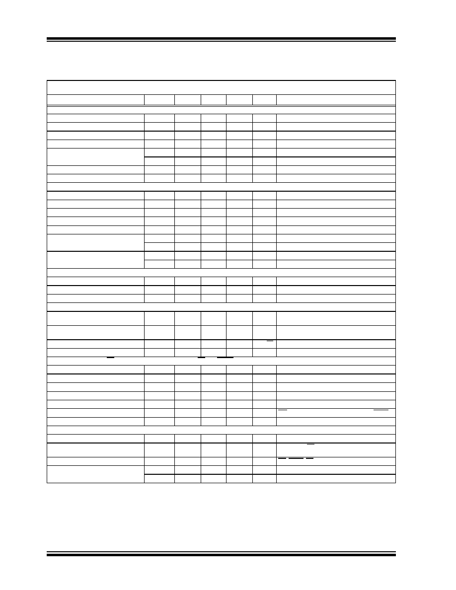
AC TIMING CHARACTERISTICS
Electrical Characteristics: Unless otherwise indicated, V
DD
= +2.7V to 5.5V, T
A
= -40�C to +85�C.
Parameter
Sym
Min.
Typ.
Max.
Units
Conditions
Clock Frequency
F
CLK
--
--
10
MHz
V
DD
= 5V (Note 1)
Clock High Time
t
HI
40
--
--
ns
Clock Low Time
t
LO
40
--
--
ns
CS Fall to First Rising CLK Edge
t
CSSR
40
--
--
ns
Data Input Setup Time
t
SU
40
--
--
ns
Data Input Hold Time
t
HD
10
--
--
ns
SCK Fall to SO Valid Propagation Delay
t
DO
--
80
ns
C
L
= 30 pF (Note 2)
SCK Rise to CS Rise Hold Time
t
CHS
30
--
--
ns
SCK Rise to CS Fall Delay
t
CS0
10
--
--
ns
CS Rise to CLK Rise Hold
t
CS1
100
--
--
ns
CS High Time
t
CSH
40
--
--
ns
Reset Pulse Width
t
RS
150
--
--
ns
Note 2
RS Rising to CS Falling Delay Time
t
RSCS
150
--
--
ns
Note 2
CS rising to RS or SHDN falling delay time
t
SE
40
--
--
ns
Note 3
CS low time
t
CSL
100
--
--
ns
Note 3
Shutdown Pulse Width
t
SH
150
--
--
ns
Note 3
Note
1:
When using the device in the daisy-chain configuration, maximum clock frequency is determined by a combination of propagation delay
time (t
DO
) and data input setup time (t
SU
). Max. clock frequency is therefore ~ 5.8 MHz based on SCK rise and fall times of 5 ns, t
HI
=
40 ns, t
DO
= 80 ns and t
SU
= 40 ns.
2:
Applies only to the MCP42XXX devices.
3:
Applies only when using hardware pins to exit software shutdown mode, MCP42XXX only.