
2004 Microchip Technology Inc.
DS21897A-page 1
MCP4921/4922
Features
∑ 12-Bit Resolution
∑ ±0.2 LSB DNL (typ)
∑ ±2 LSB INL (typ)
∑ Single or Dual Channel
∑ Rail-to-Rail Output
∑ SPITM Interface with 20 MHz Clock Support
∑ Simultaneous Latching of the Dual DACs w/LDAC
∑ Fast Settling Time of 4.5 µs
∑ Selectable Unity or 2x Gain Output
∑ 450 kHz Multiplier Mode
∑ External V
REF
Input
∑ 2.7V to 5.5V Single-Supply Operation
∑ Extended Temperature Range: -40∞C to +125∞C
Applications
∑ Set Point or Offset Trimming
∑ Sensor Calibration
∑ Digitally-Controlled Multiplier/Divider
∑ Portable Instrumentation (Battery-Powered)
∑ Motor Feedback Loop Control
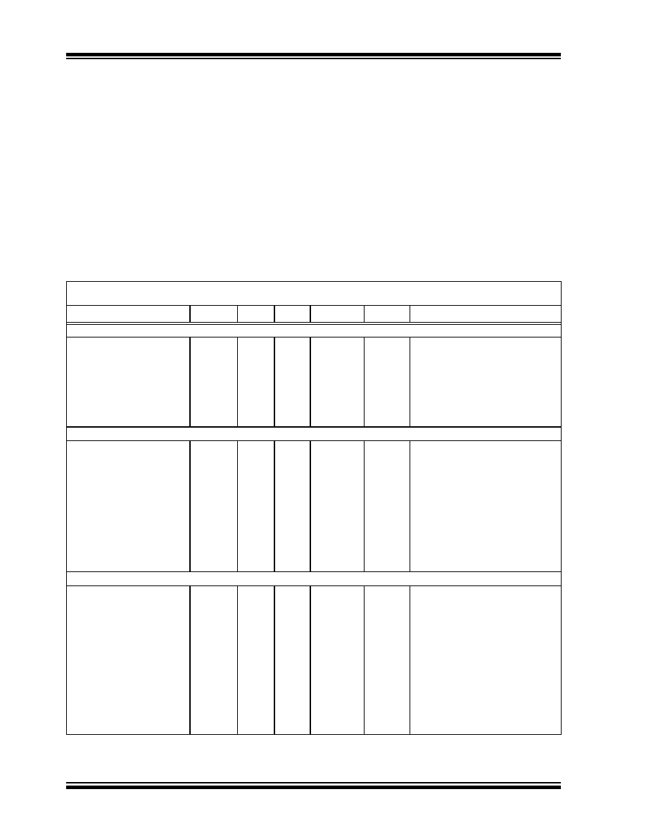
Block Diagram
Description
The Microchip Technology Inc. MCP492X are 2.7 ≠
5.5V, low-power, low DNL, 12-Bit Digital-to-Analog Con-
verters (DACs) with optional 2x buffered output and SPI
interface.
The MCP492X are DACs that provide high accuracy
and low noise performance for industrial applications
where calibration or compensation of signals (such as
temperature, pressure and humidity) are required.
The MCP492X are available in the extended tempera-
ture range and PDIP, SOIC, MSOP and TSSOP
packages.
The MCP492X devices utilize a resistive string archi-
tecture, with its inherent advantages of low DNL error,
low ratio metric temperature coefficient and fast settling
time. These devices are specified over the extended
temperature range. The MCP492X include double-
buffered inputs, allowing simultaneous updates using
the LDAC pin. These devices also incorporate a
Power-On Reset (POR) circuit to ensure reliable
power-up.
Package Types
Op Amps
V
DD
AV
SS
CS
SDI
SCK
Interface Logic
Input
Register A Register B
Input
DAC
A
Register
Register
DAC
B
String
DAC
B
String
DAC
A
V
REF
Output
Logic
Power-on
Reset
V
REF
A
B
V
OUTA
V
OUTB
LDAC
Buffer
Buffer
SHDN
Output
Gain
Logic
Gain
Logic
14
M
C
P4
921
8-Pin PDIP, SOIC, MSOP
1
2
3
4
8
7
6
5
CS
SCK
SDI
V
DD
AV
SS
V
OUTA
V
REFA
LDAC
M
C
P4
922
1
2
3
4
13
12
11
10
9
8
5
6
7
14-Pin PDIP, SOIC, TSSOP
V
DD
NC
CS
SCK
V
REFB
NC
NC
SDI
LDAC
SHDN
V
OUTB
V
OUTA
V
REFA
AV
SS
12-Bit DAC with SPITM Interface
MCP4921/4922
DS21897A-page 2
2004 Microchip Technology Inc.
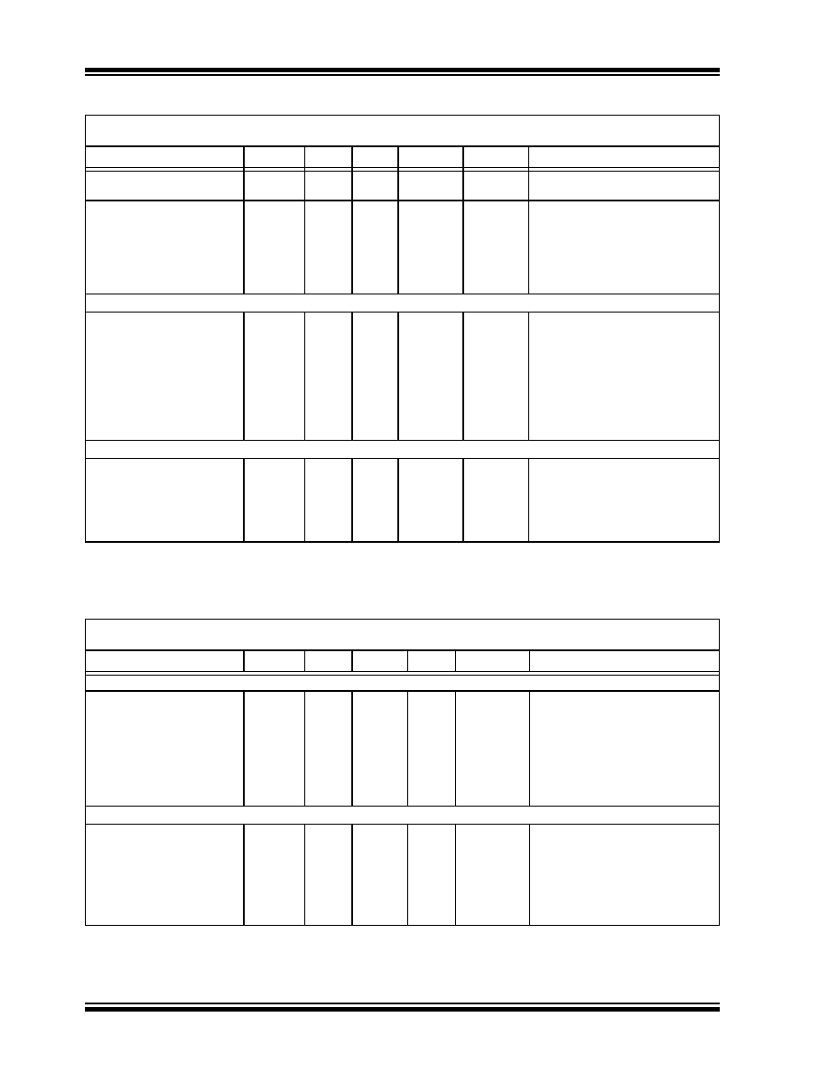
1.0
ELECTRICAL
CHARACTERISTICS
Absolute Maximum Ratings
V
DD .............................................................................................................
6.5V
All inputs and outputs w.r.t ............. AV
SS
≠0.3V to V
DD
+0.3V
Current at Input Pins ....................................................±2 mA
Current at Supply Pins ...............................................±50 mA
Current at Output Pins ...............................................±25 mA
Storage temperature .....................................-65∞C to +150∞C
Ambient temp. with power applied ................-55∞C to +125∞C
ESD protection on all pins
...........
4 kV (HBM),
400V (MM)
Maximum Junction Temperature (T
J
) . .........................+150∞C
Notice: Stresses above those listed under "Maximum Rat-
ings" may cause permanent damage to the device. This is a
stress rating only and functional operation of the device at
those or any other conditions above those indicated in the
operational listings of this specification is not implied. Expo-
sure to maximum rating conditions for extended periods may
affect device reliability.
5V AC/DC CHARACTERISTICS
Electrical Specifications: Unless otherwise indicated, V
DD
= 5V, AV
SS
= 0V, V
REF
= 2.048V, output buffer gain (G) = 2x, R
L
= 5 k
to GND, C
L
= 100 pF T
A
= -40 to +85∞C. Typical values at +25∞C.
Parameters
Sym
Min
Typ
Max
Units
Conditions
Power Requirements
Input Voltage
V
DD
2.7
--
5.5
Input Current - MCP4921
Input Current
- MCP4922
I
DD
--
--
175
350
350
700
µA
Input unbuffered, digital inputs
grounded, output unloaded,
code at 0x000
Hardware Shutdown Current
I
SHDN
--
0.3
2
µA
Software Shutdown Current
I
SHDN_SW
--
3.3
6
µA
Power-on-Reset Threshold
V
POR
--
2.0
--
V
DC Accuracy
Resolution
n
12
--
--
Bits
INL Error
INL
-12
2
12
LSB
DNL
DNL
-0.75
±0.2
+0.75
LSB
Device is Monotonic
Offset Error
V
OS
--
±0.02
1
% of FSR
Code 0x000h
Offset Error Temperature
Coefficient
V
OS
/∞C
--
0.16
--
ppm/∞C
-45∞C to 25∞C
--
-0.44
--
ppm/∞C
+25∞C to 85∞C
Gain Error
g
E
--
-0.10
1
% of FSR
Code 0xFFFh, not including offset
error.
Gain Error Temperature
Coefficient
G/∞C
--
-3
--
ppm/∞C
Input Amplifier (V
REF
Input)
Input Range - Buffered Mode
V
REF
0.040
--
V
DD
≠ 0.040
V
Note 1
Code = 2048
V
REF
= 0.2v p-p, f = 100 Hz and 1 kHz
Input Range - Unbuffered
Mode
V
REF
0
--
V
DD
V
Input Impedance
R
VREF
--
165
--
k
Unbuffered Mode
Input Capacitance -
Unbuffered Mode
C
VREF
--
7
--
pF
Multiplier Mode
-3 dB Bandwidth
f
VREF
--
450
--
kHz
V
REF
= 2.5V ±0.2Vp-p, Unbuffered,
G = 1
f
VREF
--
400
--
kHz
V
REF
= 2.5V ±0.2 Vp-p, Unbuffered,
G = 2
Multiplier Mode -
Total Harmonic Distortion
THD
VREF
--
-73
--
dB
V
REF
= 2.5V ±0.2Vp-p,
Frequency = 1 kHz
Note
1:
By design, not production tested.
2:
Too small to quantify.

2004 Microchip Technology Inc.
DS21897A-page 3
MCP4921/4922
Output Amplifier
Output Swing
V
OUT
--
0.010
to V
DD
≠ 0.040
--
Accuracy is better than 1 LSB for
V
OUT
= 10 mV to (V
DD
≠ 40 mV)
Phase Margin
m
--
66
--
degrees
Slew Rate
SR
--
0.55
--
V/µs
Short Circuit Current
I
SC
--
15
24
mA
Settling Time
t
settling
--
4.5
--
µs
Within 1/2 LSB of final value from 1/4
to 3/4 full-scale range
Dynamic Performance
DAC-to-DAC Crosstalk
--
10
--
nV-s
Note 2
Major Code Transition Glitch
--
45
--
nV-s
1 LSB change around major carry
(0111...1111 to 1000...0000)
Digital Feedthrough
--
10
--
nV-s
Note 2
Analog Crosstalk
--
10
--
nV-s
Note 2
5V AC/DC CHARACTERISTICS (CONTINUED)
Electrical Specifications: Unless otherwise indicated, V
DD
= 5V, AV
SS
= 0V, V
REF
= 2.048V, output buffer gain (G) = 2x, R
L
= 5 k
to GND, C
L
= 100 pF T
A
= -40 to +85∞C. Typical values at +25∞C.
Parameters
Sym
Min
Typ
Max
Units
Conditions
Note
1:
By design, not production tested.
2:
Too small to quantify.
3V AC/DC CHARACTERISTICS
Electrical Specifications: Unless otherwise indicated, V
DD
= 3V, AV
SS
= 0V, V
REF
= 2.048V external, output buffer gain (G) = 1x,
R
L
= 5 k
to GND, C
L
= 100 pF T
A
= -40 to +85∞C. Typical values at 25∞C
Parameters
Sym
Min
Typ
Max
Units
Conditions
Power Requirements
Input Voltage
V
DD
2.7
--
5.5
Input Current - MCP4921
Input Current
- MCP4922
I
DD
--
--
125
250
250
500
µA
Input unbuffered, digital inputs
grounded, output unloaded,
code at 0x000
Hardware Shutdown Current
I
SHDN
--
0.25
2
µA
Software Shutdown Current
I
SHDN_SW
--
2
6
µA
Power-On Reset threshold
V
POR
--
2.0
--
V
DC Accuracy
Resolution
n
12
--
--
Bits
INL Error
INL
-12
±3
+12
LSB
DNL DNL
-0.75
±0.3
+0.75
LSB
Device
is
Monotonic
Offset Error
V
OS
--
±0.02
1
% of FSR
Code 0x000h
Offset Error Temperature
Coefficient
V
OS
/∞C
--
0.5
--
ppm/∞C
-45∞C to 25∞C
--
-0.77
--
ppm/∞C
+25∞C to 85∞C
Gain Error
g
E
--
-0.15
1
% of FSR
Code 0xFFFh, not including offset
error.
Gain Error Temperature
Coefficient
G/∞C
--
-3
--
ppm/∞C
Input Amplifier (V
REF
Input)
Input Range - Buffered Mode
V
REF
0.040
--
V
DD
-0.040
V
Note 1
Code = 2048,
V
REF
= 0.2v p-p, f = 100 Hz and 1 kHz
Input Range - Unbuffered
Mode
V
REF
0
--
V
DD
V
Input Impedance
R
VREF
--
165
--
k
Unbuffered Mode
Note
1:
By design, not production tested.
2:
Too small to quantify.
MCP4921/4922
DS21897A-page 4
2004 Microchip Technology Inc.
Input Capacitance ≠
Unbuffered Mode
C
VREF
--
7
--
pF
Multiplier Mode
-3 dB Bandwidth
f
VREF
--
440
--
kHz
V
REF
= 2.048V ±0.1 Vp-p, unbuffered,
G = 1
f
VREF
--
390
--
kHz
V
REF
= 2.048V ±0.1 Vp-p, unbuffered,
G = 2
Multiplier Mode ≠
Total Harmonic Distortion
THD
VREF
--
-73
--
dB
V
REF
= 2.5V ±0.1 Vp-p,
Frequency = 1 kHz
Output Amplifier
Output Swing
V
OUT
--
0.010
to V
DD
≠ 0.040
--
Accuracy is better than 1 LSB for
V
OUT
= 10 mV to (V
DD
≠ 40 mV)
Phase Margin
m
--
66
--
degrees
Slew Rate
SR
--
0.55
--
V/µs
Short Circuit Current
I
SC
--
14
24
mA
Settling Time
t
settling
--
4.5
--
µs
Within 1/2 LSB of final value from 1/4
to 3/4 full-scale range
Dynamic Performance
DAC-to-DAC Crosstalk
--
10
--
nV-s
Note 2
Major Code Transition Glitch
--
45
--
nV-s
1 LSB change around major carry
(0111...1111 to 1000...0000)
Digital Feedthrough
--
10
--
nV-s
Note 2
Analog Crosstalk
--
10
--
nV-s
Note 2
3V AC/DC CHARACTERISTICS (CONTINUED)
Electrical Specifications: Unless otherwise indicated, V
DD
= 3V, AV
SS
= 0V, V
REF
= 2.048V external, output buffer gain (G) = 1x,
R
L
= 5 k
to GND, C
L
= 100 pF T
A
= -40 to +85∞C. Typical values at 25∞C
Parameters
Sym
Min
Typ
Max
Units
Conditions
Note
1:
By design, not production tested.
2:
Too small to quantify.
5V EXTENDED TEMPERATURE SPECIFICATIONS
Electrical Specifications: Unless otherwise indicated, V
DD
= 5V, AV
SS
= 0V, V
REF
= 2.048V, output buffer gain (G) = 2x, R
L
= 5 k
to GND, C
L
= 100 pF. Typical values at +125∞C by characterization or simulation.
Parameters
Sym
Min
Typ
Max
Units
Conditions
Power Requirements
Input Voltage
V
DD
2.7
--
5.5
Input Current - MCP4921
Input Current
- MCP4922
I
DD
--
--
200
400
--
--
µA
Input unbuffered, digital inputs
grounded, output unloaded,
code at 0x000
Hardware Shutdown Current
I
SHDN
--
1.5
--
µA
Software Shutdown Current
I
SHDN_SW
--
5
--
µA
Power-On Reset threshold
V
POR
--
1.85
--
V
DC Accuracy
Resolution
n
12
--
--
Bits
INL Error
INL
--
±4
--
LSB
DNL
DNL
--
±0.25
--
LSB
Device is Monotonic
Offset Error
V
OS
--
±0.02
--
% of FSR
Code 0x000h
Offset Error Temperature
Coefficient
V
OS
/∞C
--
-5
--
ppm/∞C
+25∞C to +125∞C
Note
1:
By design, not production tested.
2:
Too small to quantify.

2004 Microchip Technology Inc.
DS21897A-page 5
MCP4921/4922
Gain Error
g
E
--
-0.10
--
% of FSR
Code 0xFFFh, not including offset
error
Gain Error Temperature
Coefficient
G/∞C
--
-3
--
ppm/∞C
Input Amplifier (V
REF
Input)
Input Range - Buffered Mode
V
REF
--
0.040 to
V
DD
-
0.040
--
V
Note 1
Code = 2048,
V
REF
= 0.2v p-p, f = 100 Hz and 1 kHz
Input Range - Unbuffered
Mode
V
REF
0
--
V
DD
V
Input Impedance
R
VREF
--
174
--
k
Unbuffered Mode
Input Capacitance -
Unbuffered Mode
C
VREF
--
7
--
pF
Multiplying Mode
-3 dB Bandwidth
f
VREF
--
450
--
kHz
V
REF
= 2.5V ±0.1 Vp-p, Unbuffered,
G=1
f
VREF
--
400
--
kHz
V
REF
= 2.5V ±0.1 Vp-p, Unbuffered,
G = 2
Multiplying Mode - Total
Harmonic Distortion
THD
VREF
--
--
--
dB
V
REF
= 2.5V ±0.1Vp-p,
Frequency = 1 kHz
Output Amplifier
Output Swing
V
OUT
--
0.010 to
V
DD
≠
0.040
--
Accuracy is better than 1 LSB for
V
OUT
= 10 mV to (V
DD
≠ 40 mV)
Phase Margin
m
--
66
--
degrees
Slew Rate
SR
--
0.55
--
V/µs
Short Circuit Current
I
SC
--
17
--
mA
Settling Time
t
settling
--
4.5
--
µs
Within 1/2 LSB of final value from 1/4
to 3/4 full-scale range
Dynamic Performance
DAC to DAC Crosstalk
--
10
--
nV-s
Note 2
Major Code Transition Glitch
--
45
--
nV-s
1 LSB change around major carry
(0111...1111 to 1000...0000)
Digital Feedthrough
--
10
--
nV-s
Note 2
Analog Crosstalk
--
10
--
nV-s
Note 2
5V EXTENDED TEMPERATURE SPECIFICATIONS (CONTINUED)
Electrical Specifications: Unless otherwise indicated, V
DD
= 5V, AV
SS
= 0V, V
REF
= 2.048V, output buffer gain (G) = 2x, R
L
= 5 k
to GND, C
L
= 100 pF. Typical values at +125∞C by characterization or simulation.
Parameters
Sym
Min
Typ
Max
Units
Conditions
Note
1:
By design, not production tested.
2:
Too small to quantify.