600nA Rail-to-Rail Input/Output Op Amps
2002 Microchip Technology Inc.
DS21669B-page 1
M
MCP6041/2/3/4
Features
· Low Quiescent Current: 600 nA/Amplifier (typ)
· Rail-to-Rail Input: -0.3 V to V
DD
+0.3 V (max)
· Rail-to-Rail Output:
V
SS
+10 mV to V
DD
-10 mV (max)
· Gain Bandwidth Product: 14 kHz (typ)
· Wide Supply Voltage Range: 1.4 V to 5.5 V (max)
· Unity Gain Stable
· Available in Single, Dual and Quad
· Chip Select (CS) with MCP6043
· 5-lead SOT-23 package (MCP6041 only)
Applications
· Toll Booth Tags
· Wearable Products
· Temperature Measurement
· Battery Powered
Available Tools
· Spice macro models (at www.microchip.com)
· FilterLab
®
Software (at www.microchip.com)
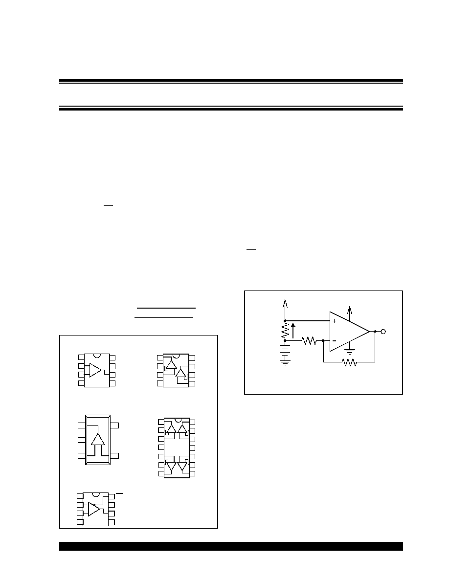
Package Types
Description
The MCP6041/2/3/4 family of operational amplifiers
from Microchip Technology, Inc. operate with a single
supply voltage as low as 1.4 V, while drawing less than
1 µA (max) of quiescent current per amplifier. These
devices are also designed to support rail-to-rail input
and output operation. This combination of features sup-
ports battery-powered and portable applications.
The MCP6041/2/3/4 amplifiers have a typical gain
bandwidth product of 14 kHz (typ) and are unity gain
stable. These specs make these operational amplifiers
appropriate for low frequency applications, such as
battery current monitoring and sensor conditioning.
The MCP6041/2/3/4 family operational amplifiers are
offered in single (MCP6041), single with a Chip Select
(CS) feature (MCP6043), dual (MCP6042) and quad
(MCP6044) configurations. The MCP6041 device is
available in the 5-lead SOT-23 package.
Typical Application
+IN
-IN
V
SS
V
DD
OUT
1
2
3
4
8
7
6
5
-
+
NC
NC
NC
+INA
-INA
V
SS
1
2
3
4
8
7
6
5
-
OUTA
+ -
+
A
B
V
DD
OUTB
-INB
+INB
+IN
-IN
V
SS
V
DD
OUT
1
2
3
4
8
7
6
5
-
+
NC
CS
NC
+INA1
-INA1
V
SS
1
2
3
4
14
13
12
11
-
OUTA
+ -
+
A
D
V
DD
OUTD
-IND
+IND
10
9
8
5
6
7
OUTB1
-INB
+INB
+INC
-INC
OUTC
+
-
B
C
-
+
MCP6041
PDIP, SOIC, MSOP
MCP6042
PDIP, SOIC, MSOP
MCP6043
PDIP, SOIC, MSOP
MCP6044
PDIP, SOIC, TSSOP
MCP6041
SOT-23-5
V
DD
+IN
1
2
3
5
-IN
V
SS
OUT
4
-
+
V
DD
10
MCP604X
100 k
1 M
V
DD
I
DD
+2.5 V
to
5.5 V
V
SS
High Side Batter
y Current Sensor
600 nA, Rail-to-Rail Input/Output Op Amps
MCP6041/2/3/4
DS21669B-page 2
2002 Microchip Technology Inc.
1.0
ELECTRICAL
CHARACTERISTICS
1.1
Maximum Ratings*
V
DD
- V
SS
......................................................................................7.0 V
All inputs and outputs................................... V
SS
0.3 V to V
DD
+0.3 V
Difference Input voltage ..................................................... |V
DD
- V
SS
|
Output Short Circuit Current ...............................................continuous
Current at Input Pins ..................................................................±2 mA
Current at Output and Supply Pins ..........................................±30 mA
Storage temperature ...................................................-65°C to +150°C
Ambient temp. with power applied ..............................-55°C to +125°C
ESD protection on all pins (HBM)
.....................................................
4 kV
*Notice: Stresses above those listed under "Maximum Ratings" may
cause permanent damage to the device. This is a stress rating only and
functional operation of the device at those or any other conditions
above those indicated in the operational listings of this specification is
not implied. Exposure to maximum rating conditions for extended peri-
ods may affect device reliability.
PIN FUNCTION TABLE
MCP6041/2/3/4 DC ELECTRICAL SPECIFICATIONS
Name
Function
+IN/+INA/+INB/+INC/+IND
Non-inverting Inputs
-IN/-INA/-INB/-INC/-IND
Inverting Inputs
V
DD
Positive Power Supply
V
SS
Negative Power Supply
OUT/OUTA/OUTB/OUTC/OUTD Outputs
CS
Chip Select
NC
No internal connection to
IC
Electrical Characteristics: Unless otherwise indicated, all limits are specified for V
DD
= +1.4 V to +5.5 V, V
SS
= GND, T
A
= 25 °C,
V
CM
= V
DD
/2, R
L
= 1 M
to V
DD
/2, and V
OUT
~ V
DD
/2
Parameters
Sym
Min
Typ
Max
Units
Conditions
Input Offset:
V
CM
= V
SS
Input Offset Voltage
V
OS
-3.0
--
+3.0
mV
Drift with Temperature
V
OS
/
T
--
±1.5
--
µV/°C
T
A
= -40°C to+85°C
Power Supply Rejection
PSRR
70
85
--
dB
Input Bias Current and Impedance:
Input Bias Current
I
B
--
1.0
--
pA
Input Bias Current Over Temperature
I
B
--
--
100
pA
T
A
= -40°C to+85°
Input Offset Current
I
OS
--
1.0
--
pA
Common Mode Input Impedance
Z
CM
--
10
13
||6
--
||pF
Differential Input Impedance
Z
DIFF
--
10
13
||6
--
||pF
Common Mode:
Common-Mode Input Range
VCMR
V
SS
-
0.3
--
V
DD
+0.3
V
Common-Mode Rejection Ratio
CMRR
62
80
--
dB
V
DD
= 5 V,
V
CM
= -0.3 V to 5.3 V
60
75
--
dB
V
DD
= 5 V,
V
CM
= 2.5 V to 5.3 V
60
80
--
dB
V
DD
= 5 V,
V
CM
= -0.3 V to 2.5 V
Open Loop Gain:
DC Open Loop Gain (large signal)
A
OL
95
115
--
dB
R
L
= 50 k
to V
DD
/2,
100 mV < V
OUT
< (V
DD
-
100 mV)
Output:
Maximum Output Voltage Swing
V
OL
, V
OH
V
SS
+ 10
--
V
DD
-
10
mV
R
L
= 50 k
to V
DD
/2
Linear Region Output Voltage Swing
V
OVR
V
SS
+ 100
--
V
DD
-
100
mV
R
L
= 50 k
to V
DD
/2,
A
OL
95 dB
Output Short Circuit Current
I
O
--
21
--
mA
V
OUT
= 2.5 V, V
DD
= 5 V
Power Supply:
Supply Voltage
V
DD
1.4
--
5.5
V
Quiescent Current per amplifier
I
Q
0.3
0.6
1.0
µA
I
O
= 0
2002 Microchip Technology Inc.
DS21669B-page 3
MCP6041/2/3/4
MCP6041/2/3/4 AC ELECTRICAL SPECIFICATIONS
SPECIFICATIONS FOR MCP6043 CHIP SELECT FEATURE
MCP6041/2/3/4 TEMPERATURE SPECIFICATIONS
Electrical Characteristics: Unless otherwise indicated, all limits are specified for V
DD
= +5 V, V
SS
= GND, T
A
= 25 °C,
V
CM
= V
DD
/2, R
L
= 1 M
to V
DD
/2, C
L
= 60 pF, and V
OUT
~ V
DD
/2
Parameters
Sym
Min
Typ
Max
Units
Conditions
Gain Bandwidth Product
GBWP
--
14
--
kHz
Slew Rate
SR
--
3.0
--
V/ms
Phase Margin
PM
--
65
--
°
G = +1
Input Voltage Noise
E
n
--
5.0
--
µVp-p
f = 0.1 Hz to 10 Hz
Input Voltage Noise Density
e
n
--
170
--
nV/
Hz
f = 1 kHz
Input Current Noise Density
i
n
--
0.6
--
fA/
Hz
f = 1 kHz
Electrical Characteristics: Unless otherwise indicated, all limits are specified for V
DD
= +1.4 V to +5.5 V, V
SS
= GND, T
A
= 25 °C,
V
CM
= V
DD
/2, R
L
= 1 M
to V
DD
/2, C
L
= 60 pF, and V
OUT
~ V
DD
/2
Parameters
Sym
Min
Typ
Max
Units
Conditions
CS Low Specifications:
CS Logic Threshold, Low
V
IL
V
SS
--
V
SS
+ 0.3
V
For entire V
DD
range
CS Input Current, Low
I
CSL
--
5.0
--
pA
CS = V
SS
CS High Specifications:
CS Logic Threshold, High
V
IH
V
DD
- 0.3
--
V
DD
V
For entire V
DD
range
CS Input Current, High
I
CSH
--
5.0
--
pA
CS = V
DD
CS Input High, GND Current
I
Q
--
20
--
pA
CS = V
DD
Amplifier Output Leakage, CS High
--
20
--
pA
CS = V
DD
Dynamic Specifications:
CS Low to Amplifier Output High
Turn-on Time
t
ON
--
2.0
50
ms
CS low = V
SS
+ 0.3 V, G = +1 V/V,
V
OUT
= 0.9 V
DD
/2
CS High to Amplifier Output High Z
t
OFF
--
10
--
µs
CS high = V
DD
- 0.3 V, G = +1 V/V
V
OUT
= 0.1 V
DD
/2
Hysteresis
V
HYST
--
0.6
--
V
V
DD
= 5 V
Electrical Characteristics: Unless otherwise indicated, all limits are specified for V
DD
= +1.4 V to +5.5 V, V
SS
= GND
Parameters
Symbol
Min
Typ
Max
Units
Conditions
Temperature Ranges:
Specified Temperature Range
T
A
-40
--
+85
°C
Operating Temperature Range
T
A
-40
--
+125
°C
Note 1
Storage Temperature Range
T
A
-65
--
+150
°C
Thermal Package Resistances:
Thermal Resistance, 5L-SOT23
JA
--
256
--
°C/W
Thermal Resistance, 8L-PDIP
JA
--
85
--
°C/W
Thermal Resistance, 8L-SOIC
JA
--
163
--
°C/W
Thermal Resistance, 8L-MSOP
JA
--
206
--
°C/W
Thermal Resistance, 14L-PDIP
JA
--
70
--
°C/W
Thermal Resistance, 14L-SOIC
JA
--
120
--
°C/W
Thermal Resistance, 14L-TSSOP
JA
--
100
--
°C/W
Note 1: The MCP6041/2/3/4 family of op amps operates over this extended range, but with reduced performance.
MCP6041/2/3/4
DS21669B-page 4
2002 Microchip Technology Inc.
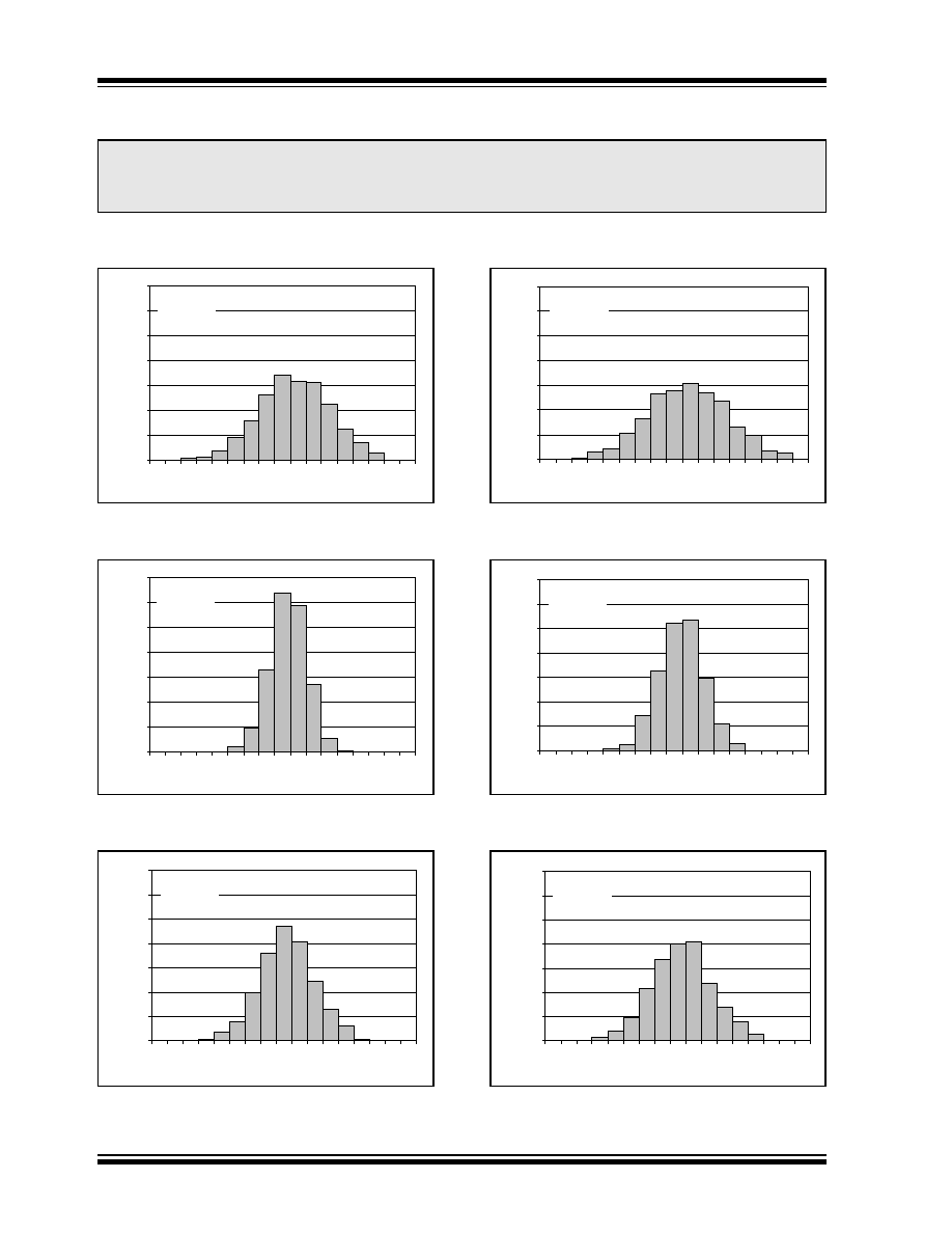
2.0
TYPICAL PERFORMANCE CURVES
Note:
Unless otherwise indicated, V
DD
= +5 V, V
SS
= GND, T
A
= 25°C, V
CM
= V
DD
/2, R
L
= 1 M
to V
DD
/2,
C
L
= 60 pF
,
and V
OUT
~ V
DD
/2.
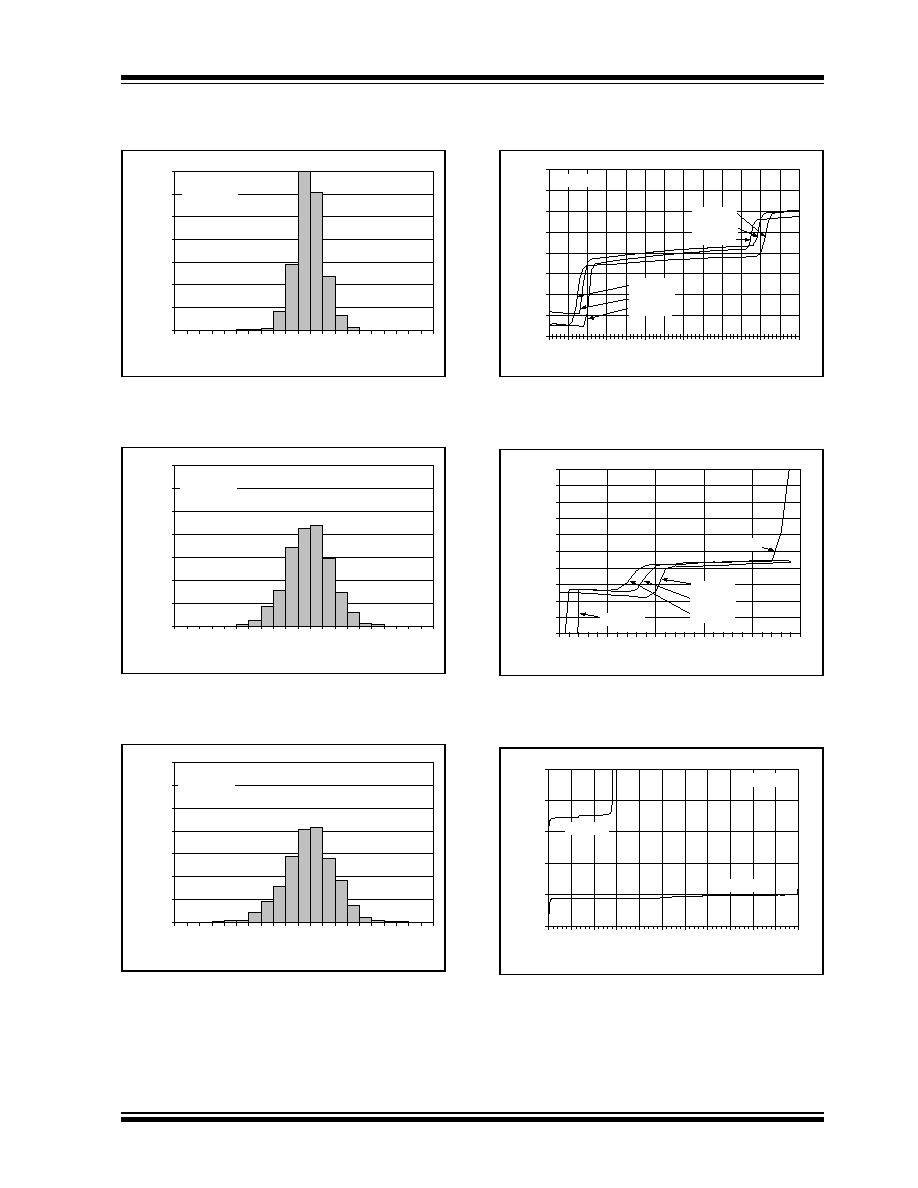
FIGURE 2-1:
Histogram of Input Offset
Voltage with V
DD
= 5.5 V, V
CM
= V
DD
.
FIGURE 2-2:
Histogram of Input Offset
Voltage with V
DD
= 5.5 V, V
CM
= V
DD
/2.
FIGURE 2-3:
Histogram of Input Offset
Voltage with V
DD
= 5.5 V, V
CM
= V
SS
.
FIGURE 2-4:
Histogram of Input Offset
Voltage with V
DD
= 1.4 V, V
CM
= V
DD
.
FIGURE 2-5:
Histogram of Input Offset
Voltage with V
DD
= 1.4 V, V
CM
= V
DD
/2.
FIGURE 2-6:
Histogram of Input Offset
Voltage with V
DD
= 1.4 V, V
CM
= V
SS
.
Note:
The graphs and tables provided following this note are a statistical summary based on a limited number of
samples and are provided for informational purposes only. The performance characteristics listed herein
are not tested or guaranteed. In some graphs or tables, the data presented may be outside the specified
operating range (e.g., outside specified power supply range) and therefore outside the warranted range.
0%
5%
10%
15%
20%
25%
30%
35%
-4.0
-3.0
-2.0
-1.0
0.0
1.0
2.0
3.0
4.0
Input Offset Voltage (mV)
Percentage
1196 Samples
V
DD
= 5.5V
V
CM
= V
DD
0%
5%
10%
15%
20%
25%
30%
35%
-4.0
-3.0
-2.0
-1.0
0.0
1.0
2.0
3.0
4.0
Input Offset Voltage (mV)
Percentage
1199 Samples
V
DD
= 5.5V
V
CM
= V
DD
/2
0%
5%
10%
15%
20%
25%
30%
35%
-4.0
-3.0
-2.0
-1.0
0.0
1.0
2.0
3.0
4.0
Input Offset Voltage (mV)
Percentage
1199 Samples
V
DD
= 5.5V
V
CM
= V
SS
0%
5%
10%
15%
20%
25%
30%
35%
-4.0
-3.0
-2.0
-1.0
0.0
1.0
2.0
3.0
4.0
Input Offset Voltage (mV)
Percentage
1196 Samples
V
DD
= 1.4V
V
CM
= V
DD
0%
5%
10%
15%
20%
25%
30%
35%
-4.0
-3.0
-2.0
-1.0
0.0
1.0
2.0
3.0
4.0
Input Offset Voltage (mV)
Percentage
1199 Samples
V
DD
= 1.4V
V
CM
= V
DD
/2
0%
5%
10%
15%
20%
25%
30%
35%
-4.0
-3.0
-2.0
-1.0
0.0
1.0
2.0
3.0
4.0
Input Offset Voltage (mV)
Percentage
1199 Samples
V
DD
= 1.4V
V
CM
= V
SS
2002 Microchip Technology Inc.
DS21669B-page 5
MCP6041/2/3/4
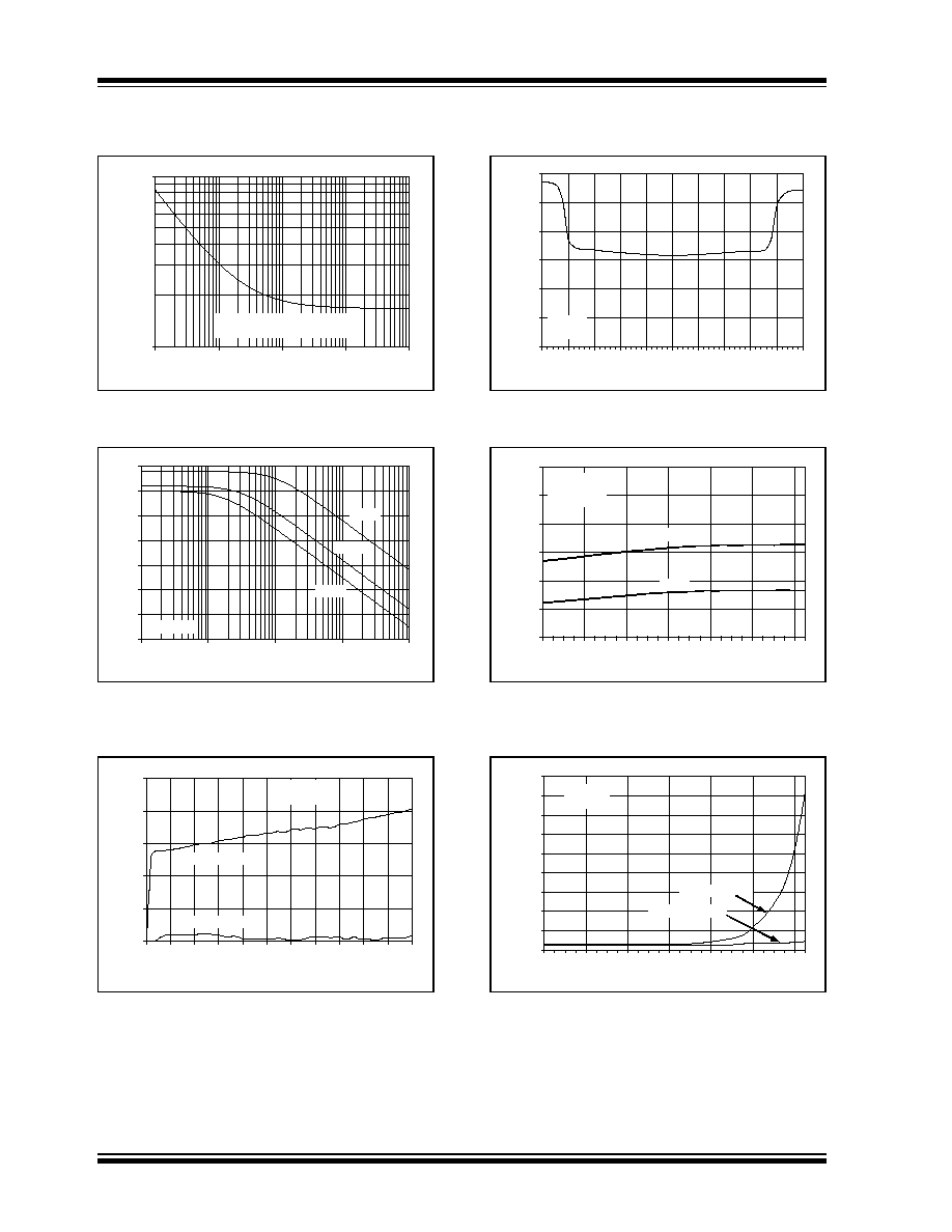
Note:
Unless otherwise indicated, V
DD
= +5 V, V
SS
= GND, T
A
= 25°C, V
CM
= V
DD
/2, R
L
= 1 M
to V
DD
/2,
C
L
= 60 pF
,
and V
OUT
~ V
DD
/2.
FIGURE 2-7:
Histogram of Input Offset
Voltage Drift with V
DD
= 5.5 V, V
CM
= V
DD
/2.
FIGURE 2-8:
Histogram of Input Offset
Voltage Drift with V
DD
= 5.5 V, V
CM
= V
SS
.
FIGURE 2-9:
Histogram of Input Offset
Voltage Drift with V
DD
= 1.4 V, V
CM
= V
SS
.
FIGURE 2-10:
Input Offset Voltage vs.
Common Mode Input Voltage vs. Temperature
with V
DD
= 5.5 V.
FIGURE 2-11:
Input Offset Voltage vs.
Common Mode Input Voltage vs. Temperature
with V
DD
= 1.4 V.
FIGURE 2-12:
Input Offset Voltage vs.
Output Voltage vs. Power Supply Voltage.
0%
5%
10%
15%
20%
25%
30%
35%
-10
-8
-6
-4
-2
0
2
4
6
8
10
Input Offset Voltage Drift (µV/°C)
Percentage
1176 Samples
V
DD
= 5.5V
V
CM
= V
DD
/2
0%
5%
10%
15%
20%
25%
30%
35%
-10
-8
-6
-4
-2
0
2
4
6
8
10
Input Offset Voltage Drift (µV/°C)
Percentage
1143 Samples
V
DD
= 5.5V
V
CM
= V
SS
0%
5%
10%
15%
20%
25%
30%
35%
-10
-8
-6
-4
-2
0
2
4
6
8
10
Input Offset Voltage Drift (µV/°C)
Percentage
1124 Samples
V
DD
= 1.4V
V
CM
= V
SS
-400
-300
-200
-100
0
100
200
300
400
-0.5 0.0 0.5 1.0 1.5 2.0 2.5 3.0 3.5 4.0 4.5 5.0 5.5 6.0
Common Mode Input Voltage (V)
Input Offset Voltage (µV)
T
A
= -40°C
V
DD
= 5.5V
T
A
= +25°C
T
A
= +85°C
T
A
= -40°C
T
A
= +25°C
T
A
= +85°C
-1000
-800
-600
-400
-200
0
200
400
600
800
1000
-0.5
0.0
0.5
1.0
1.5
2.0
Common Mode Input Voltage (V)
Input Offset Voltage (µV)
T
A
= +85°C
V
DD
= 1.4V
T
A
= -40°C
T
A
= +25°C
T
A
= +85°C
T
A
= +85°C
250
300
350
400
450
500
0.0
0.5
1.0
1.5
2.0
2.5
3.0
3.5
4.0
4.5
5.0
5.5
Output Voltage (V)
Input Offset Voltage (µV)
R
L
= 50 k
V
DD
= 5.5V
V
DD
= 1.4V
MCP6041/2/3/4
DS21669B-page 6
2002 Microchip Technology Inc.
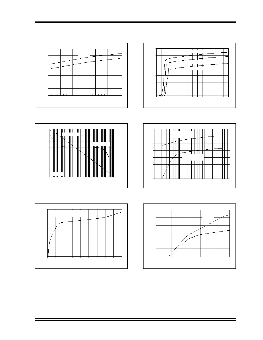
Note:
Unless otherwise indicated, V
DD
= +5 V, V
SS
= GND, T
A
= 25°C, V
CM
= V
DD
/2, R
L
= 1 M
to V
DD
/2,
C
L
= 60 pF
,
and V
OUT
~ V
DD
/2.
FIGURE 2-13:
Input Noise Voltage Density
vs. Frequency.
FIGURE 2-14:
Common Mode Rejection
Ratio, Power Supply Rejection Ratio vs.
Frequency.
FIGURE 2-15:
Input Bias, Offset Currents
vs. Common Mode Input Voltage with
Temperature = 85°C.
FIGURE 2-16:
Input Noise Voltage Density
vs. Common Mode Input Voltage.
FIGURE 2-17:
Common Mode Rejection
Ratio, Power Supply Rejection Ratio vs.
Temperature.
FIGURE 2-18:
Input Bias, Offset Currents
vs. Temperature.
100
1000
0.1
1
10
100
1000
Frequency (Hz)
e
ni
= 170 nV/ Hz, f = 1 kHz
E
ni
= 5.0 µVp-p, f = 0.1 to 10 Hz
Input Noise Voltage Density (nV/
Hz)
20
30
40
50
60
70
80
90
0.1
1
10
100
1000
Frequency (Hz)
CMRR, PSRR (dB)
V
DD
= 5.0V
CMRR
PSRR+
PSRR-
0
10
20
30
40
50
0.0
0.5
1.0
1.5
2.0
2.5
3.0
3.5
4.0
4.5
5.0
5.5
Common Mode Input Voltage (V)
Input Bias and Offset Current (pA)
Input Bias Current
Input Offset Current
T
A
= 85°C
V
DD
= 5.5V
0
50
100
150
200
250
300
0.0
0.5
1.0
1.5
2.0
2.5
3.0
3.5
4.0
4.5
5.0
Common Mode Input Voltage (V)
f = 1 kHz
V
DD
= 5V
Input Noise Voltage Density (nV/
Hz)
70
75
80
85
90
95
100
-40
-20
0
20
40
60
80
Temperature (°C)
PSRR, CMRR (dB)
PSRR
CMRR
1182 Samples
V
DD
= 5.0V
V
CM
= V
SS
0
5
10
15
20
25
30
35
40
45
-40
-20
0
20
40
60
80
Temperature ( °C)
Input Bias and Offset Current (pA)
Input Offset Current
Input Bias Current
V
DD
= 5.5V
V
CM
= V
DD
2002 Microchip Technology Inc.
DS21669B-page 7
MCP6041/2/3/4
Note:
Unless otherwise indicated, V
DD
= +5 V, V
SS
= GND, T
A
= 25°C, V
CM
= V
DD
/2, R
L
= 1 M
to V
DD
/2,
C
L
= 60 pF
,
and V
OUT
~ V
DD
/2.
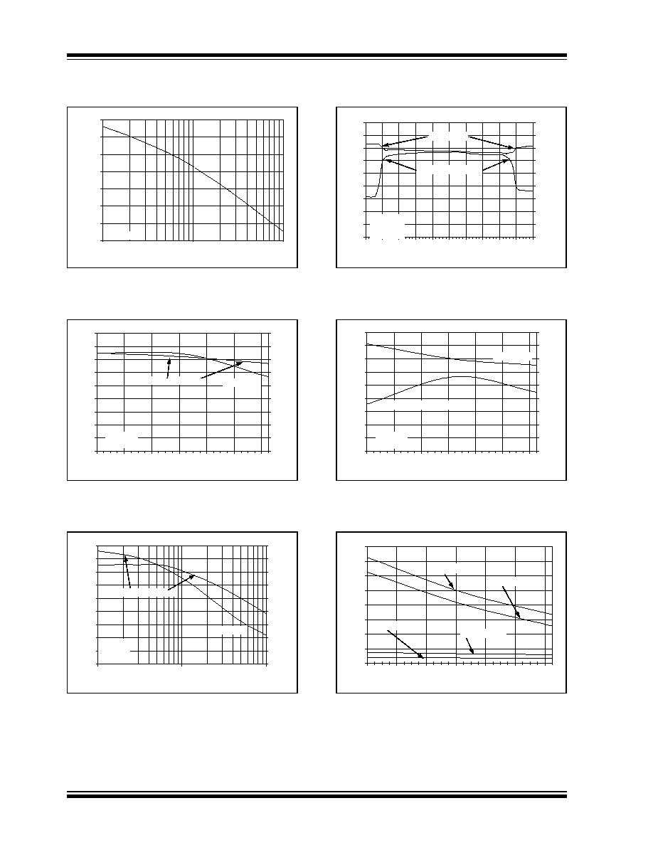
FIGURE 2-19:
Quiescent Current vs.
Temperature vs. Power Supply Voltage.
FIGURE 2-20:
Open Loop Gain, Phase vs.
Frequency with V
DD
= 5.5 V.
FIGURE 2-21:
Open Loop Gain vs. Power
Supply Voltage.
FIGURE 2-22:
Quiescent Current Vs.
Power Supply Voltage vs. Temperature.
FIGURE 2-23:
Open Loop Gain vs. Load
Resistance vs. Power Supply Voltage.
FIGURE 2-24:
Open Loop Gain vs. Output
Voltage Headroom vs. Power Supply Voltage.
0.0
0.1
0.2
0.3
0.4
0.5
0.6
0.7
-40
-20
0
20
40
60
80
Temperature (° C)
Quiescent Current (µA/Amplifier)
V
DD
= 1.4V
V
DD
= 5.5V
-20
0
20
40
60
80
100
120
140
1.E-03
1.E-02
1.E-01
1.E+00
1.E+01
1.E+02
1.E+03
1.E+04
1.E+05
Frequency (Hz)
Open Loop Gain (dB)
-240
-210
-180
-150
-120
-90
-60
-30
0
Open Loop Phase (°)
V
DD
= 5.5V
0.001 0.01
0.1
1
10
100
1k
10k 100k
Open Loop Gain
Open Loop Phase
80
90
100
110
120
130
140
1.0
1.5
2.0
2.5
3.0
3.5
4.0
4.5
5.0
5.5
Power Supply Voltage, V
DD
(V)
DC Open Loop Gain (dB)
R
L
= 50 k
V
SS
+ 100 mV < V
OUT
< V
DD
- 100 mV
0.0
0.1
0.2
0.3
0.4
0.5
0.6
0.7
0.0 0.5 1.0 1.5 2.0 2.5 3.0 3.5 4.0 4.5 5.0 5.5 6.0 6.5 7.0
Power Supply Voltage, V
DD
(V)
Quiescent Current (µA/Amplifier)
T
A
= -40°C
T
A
= +25°C
T
A
= +85°C
60
70
80
90
100
110
120
130
1. E+0 2
1. E+0 3
1. E+0 4
1. E+0 5
Load Resistance (
)
DC Open Loop Gain (dB)
V
DD
= 1.4V
V
OUT
= 0.5V to 0.9V
V
DD
= 5.5V
V
OUT
= 0.5V to 5.0V
100
1k
10k
100k
80
90
100
110
120
130
140
0.00
0.05
0.10
0.15
0.20
0.25
Output Voltage Headroom, V
DD
-V
OUT
or V
OUT
-V
SS
(V)
Open Loop Gain (dB)
R
L
= 50 k
V
DD
= 5.5V
V
DD
= 1.4V
MCP6041/2/3/4
DS21669B-page 8
2002 Microchip Technology Inc.
Note:
Unless otherwise indicated, V
DD
= +5 V, V
SS
= GND, T
A
= 25°C, V
CM
= V
DD
/2, R
L
= 1 M
to V
DD
/2,
C
L
= 60 pF
,
and V
OUT
~ V
DD
/2.
FIGURE 2-25:
Channel to Channel
Separation vs. Frequency (MCP6042 and
MCP6044 only).
FIGURE 2-26:
Gain Bandwidth Product,
Phase Margin vs. Temperature with V
DD
= 5.5 V,
Unity Gain.
FIGURE 2-27:
Unity Loop Gain Frequency,
Phase Margin vs. Load Capacitance.
FIGURE 2-28:
Gain Bandwidth Product,
Phase Margin vs. Common Mode Input Voltage
with Unity Gain.
FIGURE 2-29:
Gain Bandwidth Product,
Phase Margin vs. Temperature with V
DD
= 1.4 V,
Unity Gain.
FIGURE 2-30:
Output Short Circuit Current
vs. Temperature vs. Power Supply Voltage.
60
70
80
90
100
110
120
130
1.E+02
1.E+03
1.E+04
Frequency (Hz)
100
1k
10k
Input Referred
Channel to Channel Separation (dB)
0
2
4
6
8
10
12
14
16
18
-40
-20
0
20
40
60
80
Temperature (°C)
0
10
20
30
40
50
60
70
80
90
Phase Margin (°)
Phase Margin
Gain Bandwidth Product
V
DD
= 5.5V
G = +1 V/V
Gain Bandwidth Product (kHz)
0
2
4
6
8
10
12
14
16
18
10
100
1000
Load Capacitance (pF)
0
10
20
30
40
50
60
70
80
90
Phase Margin (°)
Unity Loop Gain Frequency
Phase Margin
V
DD
= 5.5V
G = +1 V/V
R
L
= 10 k
Unity Loop Gain Frequency (kHz)
0
2
4
6
8
10
12
14
16
18
0.0
0.5
1.0
1.5
2.0
2.5
3.0
3.5
4.0
4.5
5.0
Common Mode Input Voltage(V)
0
10
20
30
40
50
60
70
80
90
Phase Margin (°)
Phase Margin
Gain Bandwidth Product
V
DD
= 5V
R
L
= 100 k
G = +1 V/V
Gain Bandwidth Product (kHz)
0
2
4
6
8
10
12
14
16
18
-40
-20
0
20
40
60
80
Temperature (°C)
0
10
20
30
40
50
60
70
80
90
Phase Margin (°)
Phase Margin
Gain Bandwidth Product
V
DD
= 1.4V
G = +1 V/V
Gain Bandwidth Product (kHz)
0
5
10
15
20
25
30
35
40
-40
-20
0
20
40
60
80
Temperature (°C)
Output Short Circuit Current (mA)
| I
SC-
| @ V
DD
=5.5V
I
SC+
@ V
DD
=5.5V
| I
SC-
| @ V
DD
=1.4V
I
SC+
@ V
DD
=1.4V
2002 Microchip Technology Inc.
DS21669B-page 9
MCP6041/2/3/4
Note:
Unless otherwise indicated, V
DD
= +5 V, V
SS
= GND, T
A
= 25°C, V
CM
= V
DD
/2, R
L
= 1 M
to V
DD
/2,
C
L
= 60 pF
,
and V
OUT
~ V
DD
/2.
FIGURE 2-31:
Slew Rate vs. Temperature.
FIGURE 2-32:
Output Voltage Headroom
vs. Load Resistance vs. Power Supply Voltage.
FIGURE 2-33:
Small Signal Non-Inverting
Pulse Response.
FIGURE 2-34:
Output Voltage Swing vs.
Frequency vs. Power Supply Voltage.
FIGURE 2-35:
Output Voltage Headroom
vs. Temperature.
FIGURE 2-36:
Small Signal Inverting Pulse
Response.
0
1
2
3
4
5
6
-40
-20
0
20
40
60
80
Temperature (°C)
Slew Rate (V/ms)
High-to-Low Transition
Low-to-High Transition
V
DD
= 5.0V
1
10
100
1.E+03
1.E+04
1.E+05
Load Resistance ( )
Output Voltage Headroom,
V
DD
-V
OH
or V
OL
-V
SS
(mV)
V
OL
-V
SS
@ V
DD
= 5.5V
1k
10k
100k
V
OL
-V
SS
@ V
DD
= 1.4V
V
DD
-V
OH
@ V
DD
= 5.5V
V
DD
-V
OH
@ V
DD
= 1.4V
-3. E-02
-2. E-02
-2. E-02
-1. E-02
-5. E-03
0.E+00
5.E-03
1.E-02
2.E-02
2.E-02
3.E-02
0.E+00
1.E-04
2.E-04
3.E-04
4.E-04
5.E-04
6.E-04
7.E-04
8.E-04
9.E-04
1.E-03
Time (100 µs/div)
Output Voltage (5mV/div)
V
DD
= 5.0V
G = +1 V/V
R
L
= 50 k
0.1
1
10
1.E +01
1.E +02
1.E +03
1.E +04
Frequency (Hz)
Output Voltage Swing (Vp-p)
10
100
1k
10k
V
DD
= 5.5V
V
DD
= 1.4V
0
1
2
3
4
5
-40
-20
0
20
40
60
80
Temperature (°C)
Output Voltage Headroom,
V
DD
- V
OH
or V
OL
- V
SS
(mV)
V
OL
- V
SS
V
DD
- V
OH
V
DD
= 5.5V
R
L
= 50 k
-0. 025
-0. 020
-0. 015
-0. 010
-0. 005
0.000
0.005
0.010
0.015
0.020
0.025
0.0E+00
1.0E-04
2.0E-04
3.0E-04
4.0E-04
5.0E-04
6.0E-04
7.0E-04
8.0E-04
9.0E-04
1.0E-03
Time (100 µs/div)
Voltage (5 mV/div)
V
DD
= 5.0V
G = -1 V/V
R
L
= 50 k
MCP6041/2/3/4
DS21669B-page 10
2002 Microchip Technology Inc.
Note:
Unless otherwise indicated, V
DD
= +5 V, V
SS
= GND, T
A
= 25°C, V
CM
= V
DD
/2, R
L
= 1 M
to V
DD
/2,
C
L
= 60 pF
,
and V
OUT
~ V
DD
/2.
FIGURE 2-37:
Large Signal Non-Inverting
Pulse Response.
FIGURE 2-38:
Chip Select (CS) to
Amplifier Output Response Time (MCP6043
only).
FIGURE 2-39:
The MCP6041/2/3/4 family
shows no phase reversal (for information only
the Maximum Absolute Input Voltage is still
V
SS
-0.3 V and V
DD
+0.3 V).
FIGURE 2-40:
Large Signal Inverting Pulse
Response.
FIGURE 2-41:
Chip Select (CS) Hysteresis
(MCP6043 only).
0.0
0.5
1.0
1.5
2.0
2.5
3.0
3.5
4.0
4.5
5.0
0.E+00
1.E-03
2.E-03
3.E-03
4.E-03
5.E-03
6.E-03
7.E-03
8.E-03
9.E-03
1.E-02
Time (1 ms/div)
Output Voltage (V)
V
DD
= 5.0V
G = +1 V/V
R
L
= 50 k
-20.0
-17.5
-15.0
-12.5
-10.0
-7.5
-5.0
-2.5
0.0
2.5
5.0
7.5
0.E+00
1.E-03
2.E-03
3.E-03
4.E-03
5.E-03
6.E-03
7.E-03
8.E-03
9.E-03
1.E-02
Time (1 ms/div)
-1.0
-0.5
0.0
0.5
1.0
1.5
2.0
2.5
3.0
3.5
4.0
4.5
Output Voltage (V)
V
DD
= 5.0V
Chip Select (CS) Voltage (V)
V
OUT
CS
Output Hi-Z
Output Hi-Z
Output Driven
-1
0
1
2
3
4
5
6
0.00E+00
5.00E-03
1.00E-02
1.50E-02
2.00E-02
2.50E-02
Time (5 ms/div)
Output Voltage (V)
V
IN
V
DD
= 5.0V
G = +2 V/V
V
OUT
0.0
0.5
1.0
1.5
2.0
2.5
3.0
3.5
4.0
4.5
5.0
0.E+00
1.E-03
2.E-03
3.E-03
4.E-03
5.E-03
6.E-03
7.E-03
8.E-03
9.E-03
1.E-02
Time (1 ms/div)
Output Voltage (V)
V
DD
= 5.0V
G = -1 V/V
R
L
= 50 k
-0.5
0.0
0.5
1.0
1.5
2.0
2.5
3.0
0
1
2
3
4
5
CS Input Voltage (V)
Amplifier OutputActive (driven)
Amplifier OutputHi-Z
V
DD
= 5.0V
CS Input High
to Low
CS Input Low
to High
Hysteresi
s
Internal CS Switch Output (V)
2002 Microchip Technology Inc.
DS21669B-page 11
MCP6041/2/3/4
3.0
APPLICATIONS INFORMATION
The MCP6041/2/3/4 family of operational amplifiers
are fabricated on Microchip's state-of-the-art CMOS
process. They are unity gain stable and suitable for a
wide range of applications requiring very low power
consumption. With these op amps, the power supply
pin needs to be by-passed with a 0.1 µF capacitor.
3.1
Rail to Rail Input
The input stage of the family of devices uses two differ-
ential input stages in parallel; one operates at low V
CM
(common mode input voltage) and the other at high
V
CM
. With this topology, the MCP6041/2/3/4 family
operates with V
CM
up to 300 mV past either supply rail.
The Input Offset Voltage is measured at both
V
CM
= V
SS
- 0.3 V and V
DD
+ 0.3 V to ensure proper
operation.
3.2
Output Loads and Battery Life
The MCP6041/2/3/4 op amp family has outstanding
quiescent current, which supports battery-powered
applications. There is minimal quiescent current glitch-
ing when chip select (CS) is raised or lowered. This
prevents excessive current draw and reduced battery
life, when the part is turned off or on.
Heavy resistive loads at the output can cause exces-
sive battery drain. Driving a DC voltage of 2.5 V across
a 100 k
load resistor will cause the supply current to
increase by 25 µA, depleting the battery 43 times as
fast as I
Q
(0.6 µA typ) alone.
High frequency signals (fast edge rate) across capaci-
tive loads will also significantly increase supply current.
For instance, a 0.1 µF capacitor at the output presents
an AC impedance of 15.9 k
(1/2
fC) to a 100 Hz
sinewave. It can be shown that the average power
drawn from the battery by a 5.0 Vp-p sinewave
(1.77 Vrms), under these conditions, is:
EQUATION
This will drain the battery 18 times as fast as I
Q
alone.
3.3
Rail to Rail Output
The output voltage range of the MCP6041/2/3/4 family
is specified two ways. The first specification, Maximum
Output Voltage Swing, defines the maximum swing
possible under a particular output load. According to
the spec table, the output can reach
10 mV of either
supply rail when R
L
= 50 k
. See Figure 2-32 for infor-
mation on Maximum Output Voltage Swing vs. load
resistance.
The second specification, Linear Region Output Volt-
age Swing, details the output voltage range that sup-
ports the specified Open Loop Gain (A
OL
95 dB with
R
L
= 50 k
).
3.4
Input Voltage and Phase Reversal
The MCP6041/2/3/4 op amp family uses CMOS tran-
sistors at the input. It is designed to not exhibit phase
inversion when the input pins exceed the supply volt-
ages. Figure 2-39 shows an input voltage exceeding
both supplies with no resulting phase inversion.
The maximum operating V
CM
(common mode input
voltage) that can be applied to the inputs is V
SS
-0.3 V
and V
DD
+0.3 V. Voltage on the input that exceed this
absolute maximum rating can cause excessive current
to flow in or out of the input pins. Current beyond ±2 mA
can cause possible reliability problems. Applications
that exceed this rating must be externally limited with
an input resistor as shown in Figure 3-1.
FIGURE 3-1:
An input resistor, R
IN
,
should be used to limit excessive input current if
the inputs exceed the Absolute Maximum
specification.
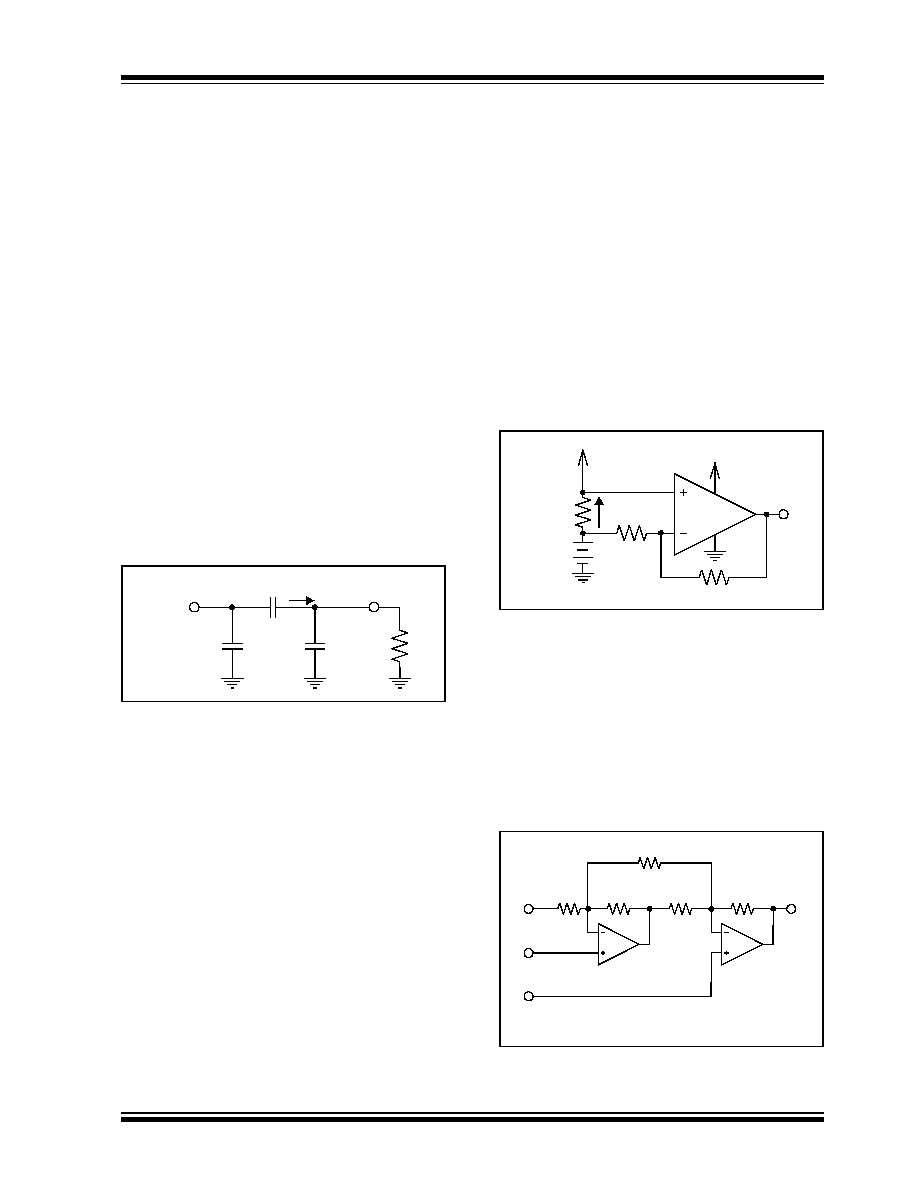
3.5
Capacitive Load and Stability
Driving capacitive loads can cause stability problems
with voltage feedback op amps. A buffer configuration
(G = +1) is the most sensitive to capacitive loads.
Figure 2-27 shows how increasing the load capaci-
tance will decrease the phase margin. While a phase
margin above 60° is ideal, 45° is sufficient. As can be
seen, up to C
L
= 150 pF can be placed on the
MCP6041/2/3/4 op amp outputs without any problems,
while 250 pF is usable with a 45° phase margin.
When the op amp is required to drive large capacitive
loads (C
L
>150 pF), a small series resistor (R
ISO
in
Figure 3-2) at the output of the amplifier improves the
phase margin. This resistor makes the output load
resistive at higher frequencies, which improves the
phase margin. The bandwidth reduction caused by the
capacitive load, however, is not changed. To select
R
ISO
, start with 1 k
, then use the MCP6041 SPICE
P
SUPPLY
V
DD
V
SS
(
)
I
Q
V
L p p
(
)
+
fC
L
(
)
=
3.0
µ
W 50
µ
W
+
=
5V
(
)
0.6
µ
A 5.0V
p p
+
100Hz 0.1
µ
F
·
·
(
)
=
R
IN
V
SS
Minimum expected V
IN
(
)
2 mA
----------------------------------------------------------------------------
R
IN
Maximum expected V
IN
(
)
V
DD
2 mA
-------------------------------------------------------------------------------
V
IN
R
IN
V
OUT
MCP604X
MCP6041/2/3/4
DS21669B-page 12
2002 Microchip Technology Inc.
macro model and bench testing to adjust R
ISO
until the
frequency response peaking is reasonable. Use the
smallest reasonable value.
FIGURE 3-2:
Amplifier circuit for heavy
capacitive loads.
3.6
The MCP6043 Chip Select (CS)
Option
The MCP6043 is a single amplifier with a chip select
(CS) option. When CS is pulled high, the supply current
drops to 20 pA (typ) and goes through the CS pin to
V
SS
. When this happens, the amplifier is put into a high
impedance state. By pulling CS low, the amplifier is
enabled. If the CS pin is left floating, the amplifier will
not operate properly. Figure 3-3 shows the output volt-
age and supply current response to a CS pulse.
FIGURE 3-3:
Timing Diagram for the CS
function on the MCP6043 op amp.
3.7
Layout Considerations
Good PC board layout techniques will help you achieve
the performance shown in the specs and Typical Per-
formance Curves. It will also assist in minimizing Elec-
tro-Magnetic Compatibility (EMC) issues.
3.7.1
SURFACE LEAKAGE
In applications where low input bias current is critical,
PC board surface leakage effects and signal coupling
from trace to trace need to be considered.
Surface leakage is caused by a difference in voltage
between traces, combined with high humidity, dust or
other contamination on the board. Under low humidity
conditions, a typical resistance between nearby traces
is 10
12
. A 5 V difference would cause 5 pA of current
to flow; this is greater than the input current of the
MCP6041/2/3/4 family at 25°C (1 pA, typ).
The simplest technique to reduce surface leakage is
using a guard ring around sensitive pins (or traces).
The guard ring is biased at the same voltage as the
sensitive pin or trace. Figure 3-4 shows an example of
a typical layout.
FIGURE 3-4:
Example of Guard Ring
layout.
Circuit schematics for different guard ring implementa-
tions are shown in Figure 3-5. Figure 3-5A biases the
guard ring to the input common mode voltage, which is
most effective for non-inverting gains, including unity
gain. Figure 3-5B biases the guard ring to a reference
voltage (V
REF
, which can be ground). This is useful for
inverting gains and precision photo sensing circuits.
FIGURE 3-5:
Two possible guard ring
connection strategies to reduce surface leakage
effects.
V
IN
R
ISO
V
OUT
MCP604X
C
L
V
IL
Hi-Z
t
ON
V
IH
CS
t
OFF
V
OUT
I
VDD
20 pA, typ
Hi-Z
I
VSS
I
CS
5 pA, typ
5 pA, typ
20 pA, typ
0.6 µA, typ
5 pA, typ
0.6 µA, typ
5 pA, typ
Guard Ring
V
SS
IN-
IN+
V
REF
MCP604X
Figure 3-5A
Figure 3-5B
V
DD
V
REF
MCP604X
V
DD
2002 Microchip Technology Inc.
DS21669B-page 13
MCP6041/2/3/4
3.7.2
COMPONENT PLACEMENT
Separate digital from analog and low speed from high
speed. This helps prevent crosstalk.
Keep sensitive traces short and straight. Separate
them from interfering components and traces. This is
especially important for high frequency (low rise time)
signals.
Use a 0.1 µF supply bypass capacitor within 0.1"
(2.5 mm) of the V
DD
pin. It must connect directly to the
ground plane.
3.7.3
SIGNAL COUPLING
The input pins of the MCP6041/2/3/4 family of op amps
are high impedance, which allows noise injection. This
noise can be capacitively or magnetically coupled. In
either case, using a ground plane helps reduce noise
injection.
When noise is coupled capacitively, the ground plane
provides shunt capacitance to ground for high fre-
quency signals. Figure 3-6 shows the equivalent cir-
cuit. The coupled current, I
M
, produces a lower voltage
(V
TRACE 2
) on the victim trace when the trace to ground
plane capacitance (C
SH2
) is large and the terminating
resistor (R
T2
) is small. Increasing the distance between
traces, and using wider traces, also helps.
FIGURE 3-6:
Equivalent circuit for
capacitive coupling between traces on a PC
board (with ground plane).
When noise is coupled magnetically, ground plane
reduces the mutual inductance between traces. This
occurs because the ground return current at high fre-
quencies will follow a path directly beneath the signal
trace. Increasing the separation between traces makes
a significant difference. Changing the direction of one
of the traces can also reduce magnetic coupling.
If these techniques are not enough, it may help to place
guard traces next to the victim trace. They should be on
both sides of the victim trace and be as close as possi-
ble. Connect the guard traces to ground plane at both
ends, and in the middle, for long traces.
3.8
Typical Applications
3.8.1
BATTERY CURRENT SENSING
The MCP6041/2/3/4 op amps' Common Mode Input
Range, which goes 300 mV beyond both supply rails,
supports their use in high side and low side battery
current sensing applications. The very low quiescent
current (0.6 µA, typ) help prolong battery life while the
rail-to-rail output allows you to detect low currents.
Figure 3-7 shows a high side battery current sensor cir-
cuit. The 10
resistors are sized to minimize power
losses. The battery current (I
DD
) through the 10
resistor causes its top terminal to be more negative
than the bottom terminal. This keeps the common
mode input voltage of the op amp
V
DD
, which is within
its allowed range. The output of the op amp can reach
V
DD
- 0.1 mV (see Figure 2-32), which is a smaller
error than the offset voltage.
FIGURE 3-7:
High Side Battery Current
Sensor.
3.8.2
INSTRUMENTATION AMPLIFIER
The MCP6041/2/3/4 op amp is well suited for condition-
ing sensor signals in battery-powered applications.
Figure 3-8 shows a two op amp instrumentation
amplifier, using the MCP6042, that works well for appli-
cations requiring rejection of common mode noise at
higher gains. The reference voltage (V
REF
) is supplied
by a low impedance source. In single supply
applications, V
REF
is typically V
DD
/2.
FIGURE 3-8:
Two Op Amp
Instrumentation Amplifier.
V
TRACE 1
R
T2
C
M
C
SH2
C
SH1
V
TRACE 2
I
M
V
DD
10
MCP604X
100 k
1 M
V
DD
I
DD
+2.5 V
to
5.5 V
V
SS
V
REF
½ MCP6042
R
1
R
G
V
OUT
R
1
R
1
R
1
V
2
V
1
½ MCP6042
V
OUT
V
1
V
2
(
)
1
R
1
R
2
------
2R
1
R
G
---------
+
+
V
REF
+
=

MCP6041/2/3/4
DS21669B-page 14
2002 Microchip Technology Inc.
4.0
SPICE MACRO MODEL
The Spice macro model for the MCP6041, MCP6042,
MCP6043 and MCP6044 simulates the typical ampli-
fier performance of: offset voltage, DC power supply
rejection, input capacitance, DC common mode rejec-
tion, open loop gain over frequency, phase margin, out-
put swing, DC power supply current, power supply
current change with supply voltage, input common
mode range, output voltage range vs. load and input
voltage noise.
The characteristics of the MCP6041, MCP6042,
MCP6043 and MCP6044 amplifiers are similar in terms
of performance and behavior. This single op amp
macro model supports all four devices with the excep-
tion of the chip select function of the MCP6043, which
is not modeled.
The listing for this macro model is shown on the next
page. The most recent revision of the model can be
downloaded from Microchip's web site at
www.microchip.com.

2002 Microchip Technology Inc.
DS21669B-page 15
MCP6041/2/3/4
Software License Agreement
The software supplied herewith by Microchip Technology Incorporated (the "Company") is intended and supplied to you, the Com-
pany's customer, for use solely and exclusively on Microchip products.
The software is owned by the Company and/or its supplier, and is protected under applicable copyright laws. All rights are reserved.
Any use in violation of the foregoing restrictions may subject the user to criminal sanctions under applicable laws, as well as to civil
liability for the breach of the terms and conditions of this license.
THIS SOFTWARE IS PROVIDED IN AN "AS IS" CONDITION. NO WARRANTIES, WHETHER EXPRESS, IMPLIED OR STATU-
TORY, INCLUDING, BUT NOT LIMITED TO, IMPLIED WARRANTIES OF MERCHANTABILITY AND FITNESS FOR A PARTICU-
LAR PURPOSE APPLY TO THIS SOFTWARE. THE COMPANY SHALL NOT, IN ANY CIRCUMSTANCES, BE LIABLE FOR
SPECIAL, INCIDENTAL OR CONSEQUENTIAL DAMAGES, FOR ANY REASON WHATSOEVER.
.SUBCKT MCP6041 1 2 3 4 5
* | | | | |
* | | | | Output
* | | | Negative Supply
* | | Positive Supply
* | Inverting Input
* Non-inverting Input
*
* Macromodel for the MCP6041/2/3/4 op amp
family:
* MCP6041 (single)
* MCP6042 (dual)
* MCP6043 (single w/ CS; chip select is not
modeled)
* MCP6044 (quad)
*
* Revision History:
* REV A: 7-9-01 created KEB
*
* Recommendations:
* Use PSPICE (other simulators may require
translation)
* For a quick, effective design, use a com-
bination of: data sheet
* specs, bench testing, and simulations
with this macromodel
* For high impedance circuits, set
GMIN=100F in the.OPTIONS
* statement
*
* Supported:
* Typical performance at room temperature
(25 degrees C)
* DC, AC, Transient, and Noise analyses.
* Most specs, including: offsets, PSRR,
CMRR, input impedance,
* open loop gain, voltage ranges, supply
current,..., etc.
*
* Not Supported:
* Chip Select (MCP6043)
* Variation in specs vs. Power Supply Volt-
age
* Distortion (detailed non-linear behavior)
* Temperature analysis
* Process variation
* Behavior outside normal operating region
*
* Input Stage
V10 3 10 -0.3
R10 10 11 78K
R11 10 12 78K
C11 11 12 4.9P
C12 1 0 6P
E12 1 14 POLY(4) 20 0 21 0 26 0 27 0 1M 1 1
1 1
G12 14 0 POLY(2) 22 0 23 0 1.5P 1U 1U
M12 11 14 15 15 NMI
C13 14 2 3P
M14 12 2 15 15 NMI
G14 2 0 POLY(2) 24 0 25 0 0.5P 1U 1U
C14 2 0 6P
I15 15 4 500N
V16 16 4 0.18
D16 16 15 DL
V13 3 13 0.00
D13 14 13 DL
*
* Noise Sources
I20 21 20 17.2N
D20 20 0 DN1
D21 0 21 DN1
I22 23 22 588U
D22 22 0 DN23
D23 0 23 DN23
I24 25 24 588U
D24 24 0 DN23
D25 0 25 DN23
*
* PSRR and CMRR
G26 0 26 POLY(1) 3 4 110U -20U
R26 26 0 1
G27 0 27 POLY(2) 1 3 2 4 -275U 50U 50U
R27 27 0 1
*
* Open Loop Gain, Slew Rate
G30 0 30 POLY(1) 12 11 0 1MEG
R30 30 0 1
C30 30 0 11.4
G31 0 31 POLY(1) 30 0 0 1
R31 31 0 1
C31 31 0 775N
*
* Output Stage
G40 0 40 POLY(1) 45 5 0 22.7M
D41 40 41 DL
R41 41 0 1K
D42 42 40 DL
R42 42 0 1K
G43 3 0 POLY(1) 41 0 100N 1M
G47 0 4 POLY(1) 42 0 100N -1M
E43 43 0 POLY(1) 3 0 0 1

MCP6041/2/3/4
DS21669B-page 16
2002 Microchip Technology Inc.
E47 47 0 POLY(1) 4 0 0 1
V44 43 44 1M
D44 45 44 DLS
D46 46 45 DLS
V46 46 47 1M
G45 47 45 POLY(2) 31 0 3 4 0 8U 4U
R45 45 47 125K
R48 45 5 44
C48 5 0 2P
*
* Models
.MODEL NMI NMOS L=2 W=42
.MODEL DL D N=1 IS=1F
.MODEL DLS D N=1M IS=1F
.MODEL DN1 D IS=1F KF=1.13E-18 AF=1
.MODEL DN23 D IS=1F KF=3E-20 AF=1
*
.ENDS MCP6041
2002 Microchip Technology Inc.
DS21669B-page 17
MCP6041/2/3/4
5.0
PACKAGING INFORMATION
5.1
Package Marking Information
XXXXXXXX
XXXXXNNN
YYWW
8-Lead PDIP (300 mil)
Example:
8-Lead SOIC (150 mil)
Example:
XXXXXXXX
XXXXYYWW
NNN
Legend: XX...X Customer specific information*
YY
Year code (last 2 digits of calendar year)
WW
Week code (week of January 1 is week `01')
NNN
Alphanumeric traceability code
Note:
In the event the full Microchip part number cannot be marked on one line, it will
be carried over to the next line thus limiting the number of available characters
for customer specific information.
*
Standard marking consists of Microchip part number, year code, week code, traceability code (facility
code, mask rev#, and assembly code). For marking beyond this, certain price adders apply. Please
check with your Microchip Sales Office.
MCP6041
I/PNNN
YYWW
MCP6041
I/SNYYWW
NNN
8-Lead MSOP
Example:
XXXXXX
YWWNNN
6041
YWWNNN
1
2
3
5
4
5-Lead SOT-23 (MCP6041 only)
Example:
XXNN
1
2
3
5
4
SBNN
MCP6041/2/3/4
DS21669B-page 18
2002 Microchip Technology Inc.
5.1
Package Marking Information (Continued)
14-Lead PDIP (300 mil) (MCP6044)
Example:
14-Lead TSSOP (MCP6044)
Example:
14-Lead SOIC (150 mil) (MCP6044)
Example:
XXXXXXXXXXXXXX
XXXXXXXXXXXXXX
YYWWNNN
XXXXXXXXXX
YYWWNNN
XXXXXX
YYWW
NNN
Legend: XX...X Customer specific information*
YY
Year code (last 2 digits of calendar year)
WW
Week code (week of January 1 is week `01')
NNN
Alphanumeric traceability code
Note:
In the event the full Microchip part number cannot be marked on one line, it will
be carried over to the next line thus limiting the number of available characters
for customer specific information.
*
Standard marking consists of Microchip part number, year code, week code, traceability code (facility
code, mask rev#, and assembly code). For marking beyond this, certain price adders apply. Please
check with your Microchip Sales Office.
MCP6044-I/P
XXXXXXXXXXXXXX
YYWWNNN
6044ST
YYWW
NNN
XXXXXXXXXX
MCP6044ISL
YYWWNNN
XXXXXXXXXX
2002 Microchip Technology Inc.
DS21669B-page 19
MCP6041/2/3/4
8-Lead Plastic Dual In-line (P) 300 mil (PDIP)
B1
B
A1
A
L
A2
p
E
eB
c
E1
n
D
1
2
Units
INCHES*
MILLIMETERS
Dimension Limits
MIN
NOM
MAX
MIN
NOM
MAX
Number of Pins
n
8
8
Pitch
p
.100
2.54
Top to Seating Plane
A
.140
.155
.170
3.56
3.94
4.32
Molded Package Thickness
A2
.115
.130
.145
2.92
3.30
3.68
Base to Seating Plane
A1
.015
0.38
Shoulder to Shoulder Width
E
.300
.313
.325
7.62
7.94
8.26
Molded Package Width
E1
.240
.250
.260
6.10
6.35
6.60
Overall Length
D
.360
.373
.385
9.14
9.46
9.78
Tip to Seating Plane
L
.125
.130
.135
3.18
3.30
3.43
Lead Thickness
c
.008
.012
.015
0.20
0.29
0.38
Upper Lead Width
B1
.045
.058
.070
1.14
1.46
1.78
Lower Lead Width
B
.014
.018
.022
0.36
0.46
0.56
Overall Row Spacing
§
eB
.310
.370
.430
7.87
9.40
10.92
Mold Draft Angle Top
5
10
15
5
10
15
Mold Draft Angle Bottom
5
10
15
5
10
15
* Controlling Parameter
Notes:
Dimensions D and E1 do not include mold flash or protrusions. Mold flash or protrusions shall not exceed
JEDEC Equivalent: MS-001
Drawing No. C04-018
.010" (0.254mm) per side.
§ Significant Characteristic
MCP6041/2/3/4
DS21669B-page 20
2002 Microchip Technology Inc.
8-Lead Plastic Small Outline (SN) Narrow, 150 mil (SOIC)
Foot Angle
0
4
8
0
4
8
15
12
0
15
12
0
Mold Draft Angle Bottom
15
12
0
15
12
0
Mold Draft Angle Top
0.51
0.42
0.33
.020
.017
.013
B
Lead Width
0.25
0.23
0.20
.010
.009
.008
c
Lead Thickness
0.76
0.62
0.48
.030
.025
.019
L
Foot Length
0.51
0.38
0.25
.020
.015
.010
h
Chamfer Distance
5.00
4.90
4.80
.197
.193
.189
D
Overall Length
3.99
3.91
3.71
.157
.154
.146
E1
Molded Package Width
6.20
6.02
5.79
.244
.237
.228
E
Overall Width
0.25
0.18
0.10
.010
.007
.004
A1
Standoff §
1.55
1.42
1.32
.061
.056
.052
A2
Molded Package Thickness
1.75
1.55
1.35
.069
.061
.053
A
Overall Height
1.27
.050
p
Pitch
8
8
n
Number of Pins
MAX
NOM
MIN
MAX
NOM
MIN
Dimension Limits
MILLIMETERS
INCHES*
Units
2
1
D
n
p
B
E
E1
h
L
c
45
°
A2
A
A1
* Controlling Parameter
Notes:
Dimensions D and E1 do not include mold flash or protrusions. Mold flash or protrusions shall not exceed
.010" (0.254mm) per side.
JEDEC Equivalent: MS-012
Drawing No. C04-057
§ Significant Characteristic
2002 Microchip Technology Inc.
DS21669B-page 21
MCP6041/2/3/4
8-Lead Plastic Micro Small Outline Package (MS) (MSOP)
p
A
A1
A2
D
L
c
Dimensions D and E1 do not include mold flash or protrusions. Mold flash or protrusions shall not
.037
.035
F
Footprint (Reference)
exceed .010" (0.254mm) per side.
Notes:
Drawing No. C04-111
*Controlling Parameter
Mold Draft Angle Top
Mold Draft Angle Bottom
Foot Angle
Lead Width
Lead Thickness
c
B
7
7
.004
.010
0
.006
.012
(F)
Dimension Limits
Overall Height
Molded Package Thickness
Molded Package Width
Overall Length
Foot Length
Standoff §
Overall Width
Number of Pins
Pitch
A
L
E1
D
A1
E
A2
.016
.114
.114
.022
.118
.118
.002
.030
.193
.034
MIN
p
n
Units
.026
NOM
8
INCHES
1.00
0.95
0.90
.039
0.15
0.30
.008
.016
6
0.10
0.25
0
7
7
0.20
0.40
6
MILLIMETERS*
0.65
0.86
3.00
3.00
0.55
4.90
.044
.122
.028
.122
.038
.006
0.40
2.90
2.90
0.05
0.76
MIN
MAX
NOM
1.18
0.70
3.10
3.10
0.15
0.97
MAX
8
E1
E
B
n
1
2
§ Significant Characteristic
.184
.200
4.67
.5.08
MCP6041/2/3/4
DS21669B-page 22
2002 Microchip Technology Inc.
5-Lead Plastic Small Outline Transistor (OT) (SOT23)
10
5
0
10
5
0
Mold Draft Angle Bottom
10
5
0
10
5
0
Mold Draft Angle Top
0.50
0.43
0.35
.020
.017
.014
B
Lead Width
0.20
0.15
0.09
.008
.006
.004
c
Lead Thickness
10
5
0
10
5
0
Foot Angle
0.55
0.45
0.35
.022
.018
.014
L
Foot Length
3.10
2.95
2.80
.122
.116
.110
D
Overall Length
1.75
1.63
1.50
.069
.064
.059
E1
Molded Package Width
3.00
2.80
2.60
.118
.110
.102
E
Overall Width
0.15
0.08
0.00
.006
.003
.000
A1
Standoff §
1.30
1.10
0.90
.051
.043
.035
A2
Molded Package Thickness
1.45
1.18
0.90
.057
.046
.035
A
Overall Height
1.90
.075
p1
Outside lead pitch (basic)
0.95
.038
p
Pitch
5
5
n
Number of Pins
MAX
NOM
MIN
MAX
NOM
MIN
Dimension Limits
MILLIMETERS
INCHES*
Units
1
p
D
B
n
E
E1
L
c
A2
A
A1
p1
* Controlling Parameter
Notes:
Dimensions D and E1 do not include mold flash or protrusions. Mold flash or protrusions shall not exceed
.010" (0.254mm) per side.
JEDEC Equivalent: MO-178
Drawing No. C04-091
§ Significant Characteristic
2002 Microchip Technology Inc.
DS21669B-page 23
MCP6041/2/3/4
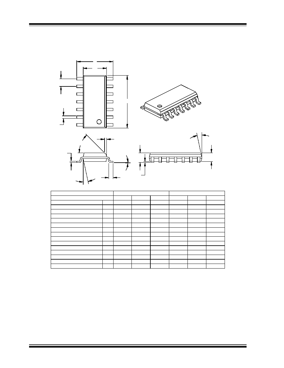
14-Lead Plastic Dual In-line (P) 300 mil (PDIP)
E1
n
D
1
2
eB
E
c
A
A1
B
B1
L
A2
p
Units
INCHES*
MILLIMETERS
Dimension Limits
MIN
NOM
MAX
MIN
NOM
MAX
Number of Pins
n
14
14
Pitch
p
.100
2.54
Top to Seating Plane
A
.140
.155
.170
3.56
3.94
4.32
Molded Package Thickness
A2
.115
.130
.145
2.92
3.30
3.68
Base to Seating Plane
A1
.015
0.38
Shoulder to Shoulder Width
E
.300
.313
.325
7.62
7.94
8.26
Molded Package Width
E1
.240
.250
.260
6.10
6.35
6.60
Overall Length
D
.740
.750
.760
18.80
19.05
19.30
Tip to Seating Plane
L
.125
.130
.135
3.18
3.30
3.43
Lead Thickness
c
.008
.012
.015
0.20
0.29
0.38
Upper Lead Width
B1
.045
.058
.070
1.14
1.46
1.78
Lower Lead Width
B
.014
.018
.022
0.36
0.46
0.56
Overall Row Spacing
§
eB
.310
.370
.430
7.87
9.40
10.92
Mold Draft Angle Top
5
10
15
5
10
15
5
10
15
5
10
15
Mold Draft Angle Bottom
* Controlling Parameter
Notes:
Dimensions D and E1 do not include mold flash or protrusions. Mold flash or protrusions shall not exceed
.010" (0.254mm) per side.
JEDEC Equivalent: MS-001
Drawing No. C04-005
§ Significant Characteristic
MCP6041/2/3/4
DS21669B-page 24
2002 Microchip Technology Inc.
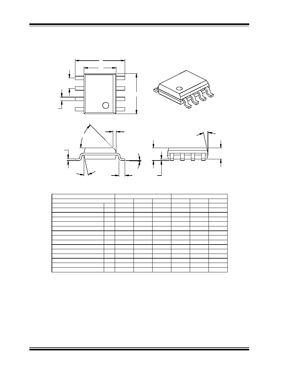
14-Lead Plastic Small Outline (SL) Narrow, 150 mil (SOIC)
Foot Angle
0
4
8
0
4
8
15
12
0
15
12
0
Mold Draft Angle Bottom
15
12
0
15
12
0
Mold Draft Angle Top
0.51
0.42
0.36
.020
.017
.014
B
Lead Width
0.25
0.23
0.20
.010
.009
.008
c
Lead Thickness
1.27
0.84
0.41
.050
.033
.016
L
Foot Length
0.51
0.38
0.25
.020
.015
.010
h
Chamfer Distance
8.81
8.69
8.56
.347
.342
.337
D
Overall Length
3.99
3.90
3.81
.157
.154
.150
E1
Molded Package Width
6.20
5.99
5.79
.244
.236
.228
E
Overall Width
0.25
0.18
0.10
.010
.007
.004
A1
Standoff §
1.55
1.42
1.32
.061
.056
.052
A2
Molded Package Thickness
1.75
1.55
1.35
.069
.061
.053
A
Overall Height
1.27
.050
p
Pitch
14
14
n
Number of Pins
MAX
NOM
MIN
MAX
NOM
MIN
Dimension Limits
MILLIMETERS
INCHES*
Units
2
1
D
p
n
B
E
E1
h
L
c
45
°
A2
A
A1
* Controlling Parameter
Notes:
Dimensions D and E1 do not include mold flash or protrusions. Mold flash or protrusions shall not exceed
.010" (0.254mm) per side.
JEDEC Equivalent: MS-012
Drawing No. C04-065
§ Significant Characteristic
2002 Microchip Technology Inc.
DS21669B-page 25
MCP6041/2/3/4
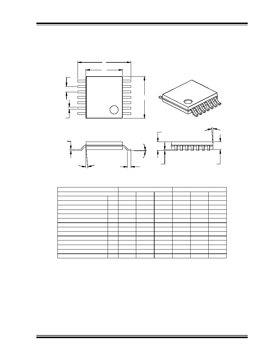
14-Lead Plastic Thin Shrink Small Outline (ST) 4.4 mm (TSSOP)
8
4
0
8
4
0
Foot Angle
10
5
0
10
5
0
Mold Draft Angle Bottom
10
5
0
10
5
0
Mold Draft Angle Top
0.30
0.25
0.19
.012
.010
.007
B1
Lead Width
0.20
0.15
0.09
.008
.006
.004
c
Lead Thickness
0.70
0.60
0.50
.028
.024
.020
L
Foot Length
5.10
5.00
4.90
.201
.197
.193
D
Molded Package Length
4.50
4.40
4.30
.177
.173
.169
E1
Molded Package Width
6.50
6.38
6.25
.256
.251
.246
E
Overall Width
0.15
0.10
0.05
.006
.004
.002
A1
Standoff §
0.95
0.90
0.85
.037
.035
.033
A2
Molded Package Thickness
1.10
.043
A
Overall Height
0.65
.026
p
Pitch
14
14
n
Number of Pins
MAX
NOM
MIN
MAX
NOM
MIN
Dimension Limits
MILLIMETERS*
INCHES
Units
L
c
2
1
D
n
B
p
E1
E
A2
A1
A
* Controlling Parameter
Notes:
Dimensions D and E1 do not include mold flash or protrusions. Mold flash or protrusions shall not exceed
.005" (0.127mm) per side.
JEDEC Equivalent: MO-153
Drawing No. C04-087
§ Significant Characteristic

MCP6041/2/3/4
DS21669B-page 26
2002 Microchip Technology Inc.
NOTES:

2002 Microchip Technology Inc.
DS21669B-page 27
MCP6041/2/3/4
Systems Information and Upgrade Hot Line
The Systems Information and Upgrade Line provides
system users a listing of the latest versions of all of
Microchip's development systems software products.
Plus, this line provides information on how customers
can receive any currently available upgrade kits.The
Hot Line Numbers are:
1-800-755-2345 for U.S. and most of Canada, and
1-480-792-7302 for the rest of the world.
ON-LINE SUPPORT
Microchip provides on-line support on the Microchip
World Wide Web (WWW) site.
The web site is used by Microchip as a means to make
files and information easily available to customers. To
view the site, the user must have access to the Internet
and a web browser, such as Netscape or Microsoft
Explorer. Files are also available for FTP download
from our FTP site.
Connecting to the Microchip Internet Web Site
The Microchip web site is available by using your
favorite Internet browser to attach to:
www.microchip.com
The file transfer site is available by using an FTP ser-
vice to connect to:
ftp://ftp.microchip.com
The web site and file transfer site provide a variety of
services. Users may download files for the latest
Development Tools, Data Sheets, Application Notes,
User's Guides, Articles and Sample Programs. A vari-
ety of Microchip specific business information is also
available, including listings of Microchip sales offices,
distributors and factory representatives. Other data
available for consideration is:
· Latest Microchip Press Releases
· Technical Support Section with Frequently Asked
Questions
· Design Tips
· Device Errata
· Job Postings
· Microchip Consultant Program Member Listing
· Links to other useful web sites related to
Microchip Products
· Conferences for products, Development Systems,
technical information and more
· Listing of seminars and events
013001

MCP6041/2/3/4
DS21669B-page 28
2002 Microchip Technology Inc.
READER RESPONSE
It is our intention to provide you with the best documentation possible to ensure successful use of your Microchip prod-
uct. If you wish to provide your comments on organization, clarity, subject matter, and ways in which our documentation
can better serve you, please FAX your comments to the Technical Publications Manager at (480) 792-4150.
Please list the following information, and use this outline to provide us with your comments about this Data Sheet.
1. What are the best features of this document?
2. How does this document meet your hardware and software development needs?
3. Do you find the organization of this data sheet easy to follow? If not, why?
4. What additions to the data sheet do you think would enhance the structure and subject?
5. What deletions from the data sheet could be made without affecting the overall usefulness?
6. Is there any incorrect or misleading information (what and where)?
7. How would you improve this document?
8. How would you improve our software, systems, and silicon products?
To:
Technical Publications Manager
RE:
Reader Response
Total Pages Sent
From: Name
Company
Address
City / State / ZIP / Country
Telephone: (_______) _________ - _________
Application (optional):
Would you like a reply? Y N
Device:
Literature Number:
Questions:
FAX: (______) _________ - _________
DS21669B
MCP6041/2/3/4
2002 Microchip Technology Inc.
DS21669B-page 29
MCP6041/2/3/4
PRODUCT IDENTIFICATION SYSTEM
To order or obtain information, e.g., on pricing or delivery, refer to the factory or the listed sales office.
Sales and Support
Data Sheets
Products supported by a preliminary Data Sheet may have an errata sheet describing minor operational differences and recom-
mended workarounds. To determine if an errata sheet exists for a particular device, please contact one of the following:
1.
Your local Microchip sales office
2.
The Microchip Corporate Literature Center U.S. FAX: (480) 792-7277
3.
The Microchip Worldwide Site (www.microchip.com)
Please specify which device, revision of silicon and Data Sheet (include Literature #) you are using.
New Customer Notification System
Register on our web site (www.microchip.com/cn) to receive the most current information on our products.
PART NO.
X
/XX
Package
Temperature
Range
Device
Device:
MCP6041:
CMOS Single Op Amp
MCP6041T: CMOS Single Op Amp
(Tape and Reel for SOT-23, SOIC, MSOP)
MCP6042:
CMOS Dual Op Amp
MCP6042T: CMOS Dual Op Amp
(Tape and Reel for SOIC and TSSOP)
MCP6043:
CMOS Single Op Amp w/CS Function
MCP6043T: CMOS Single Op Amp w/CS Function
(Tape and Reel for SOIC and MSOP)
MCP6044:
CMOS Quad Op Amp
MCP6044T: CMOS Quad Op Amp
(Tape and Reel for SOIC and TSSOP)
Temperature Range:
I
=
-40°C to +85°C
Package:
MS
=
Plastic MSOP, 8-lead
P
=
Plastic DIP (300 mil Body), 8-lead, 14-lead
SN
=
Plastic SOIC (150 mil Body), 8-lead
OT
=
Plastic Small Outline Transistor (SOT-23),
5-lead (Tape and Reel - MCP6041 only)
SL
=
Plastic SOIC (150 mil Body), 14-lead
ST
=
Plastic TSSOP (4.4mm Body), 14-lead
Examples:
a)
MCP6041-I/P:
Industrial temperature,
PDIP package.
b)
MCP6041T-I/OT: Tape and Reel, Indus-
trial temperature, SOT-23 package.
c)
MCP6042-I/SN:
Industrial temperature,
SOIC package.
d)
MCP6043-I/MS:
Industrial temperature,
MSOP package.
e)
MCP6044-I/SL:
Industrial temperature,
SIOC package.
f)
MCP6044-I/ST:
Industrial temperature,
TSSOP package.

MCP6041/2/3/4
DS21669B-page 30
2002 Microchip Technology Inc.
NOTES:
2002 Microchip Technology Inc.
DS21669B - page 31
Information contained in this publication regarding device
applications and the like is intended through suggestion only
and may be superseded by updates. It is your responsibility to
ensure that your application meets with your specifications.
No representation or warranty is given and no liability is
assumed by Microchip Technology Incorporated with respect
to the accuracy or use of such information, or infringement of
patents or other intellectual property rights arising from such
use or otherwise. Use of Microchip's products as critical com-
ponents in life support systems is not authorized except with
express written approval by Microchip. No licenses are con-
veyed, implicitly or otherwise, under any intellectual property
rights.
Trademarks
The Microchip name and logo, the Microchip logo, FilterLab,
K
EE
L
OQ
, microID, MPLAB, PIC, PICmicro, PICMASTER,
PICSTART, PRO MATE, SEEVAL and The Embedded Control
Solutions Company are registered trademarks of Microchip Tech-
nology Incorporated in the U.S.A. and other countries.
dsPIC, ECONOMONITOR, FanSense, FlexROM, fuzzyLAB,
In-Circuit Serial Programming, ICSP, ICEPIC, microPort,
Migratable Memory, MPASM, MPLIB, MPLINK, MPSIM,
MXDEV, MXLAB, PICC, PICDEM, PICDEM.net, rfPIC, Select
Mode and Total Endurance are trademarks of Microchip
Technology Incorporated in the U.S.A.
Serialized Quick Turn Programming (SQTP) is a service mark
of Microchip Technology Incorporated in the U.S.A.
All other trademarks mentioned herein are property of their
respective companies.
© 2002, Microchip Technology Incorporated, Printed in the
U.S.A., All Rights Reserved.
Printed on recycled paper.
Microchip received QS-9000 quality system
certification for its worldwide headquarters,
design and wafer fabrication facilities in
Chandler and Tempe, Arizona in July 1999
and Mountain View, California in March 2002.
The Company's quality system processes and
procedures are QS-9000 compliant for its
PICmicro
®
8-bit MCUs, K
EE
L
OQ
®
code hopping
devices, Serial EEPROMs, microperipherals,
non-volatile memory and analog products. In
addition, Microchip's quality system for the
design and manufacture of development
systems is ISO 9001 certified.

DS21669B-page 32
2002 Microchip Technology Inc.
M
AMERICAS
Corporate Office
2355 West Chandler Blvd.
Chandler, AZ 85224-6199
Tel: 480-792-7200 Fax: 480-792-7277
Technical Support: 480-792-7627
Web Address: http://www.microchip.com
Rocky Mountain
2355 West Chandler Blvd.
Chandler, AZ 85224-6199
Tel: 480-792-7966 Fax: 480-792-4338
Atlanta
500 Sugar Mill Road, Suite 200B
Atlanta, GA 30350
Tel: 770-640-0034 Fax: 770-640-0307
Boston
2 Lan Drive, Suite 120
Westford, MA 01886
Tel: 978-692-3848 Fax: 978-692-3821
Chicago
333 Pierce Road, Suite 180
Itasca, IL 60143
Tel: 630-285-0071 Fax: 630-285-0075
Dallas
4570 Westgrove Drive, Suite 160
Addison, TX 75001
Tel: 972-818-7423 Fax: 972-818-2924
Detroit
Tri-Atria Office Building
32255 Northwestern Highway, Suite 190
Farmington Hills, MI 48334
Tel: 248-538-2250 Fax: 248-538-2260
Kokomo
2767 S. Albright Road
Kokomo, Indiana 46902
Tel: 765-864-8360 Fax: 765-864-8387
Los Angeles
18201 Von Karman, Suite 1090
Irvine, CA 92612
Tel: 949-263-1888 Fax: 949-263-1338
New York
150 Motor Parkway, Suite 202
Hauppauge, NY 11788
Tel: 631-273-5305 Fax: 631-273-5335
San Jose
Microchip Technology Inc.
2107 North First Street, Suite 590
San Jose, CA 95131
Tel: 408-436-7950 Fax: 408-436-7955
Toronto
6285 Northam Drive, Suite 108
Mississauga, Ontario L4V 1X5, Canada
Tel: 905-673-0699 Fax: 905-673-6509
ASIA/PACIFIC
Australia
Microchip Technology Australia Pty Ltd
Suite 22, 41 Rawson Street
Epping 2121, NSW
Australia
Tel: 61-2-9868-6733 Fax: 61-2-9868-6755
China - Beijing
Microchip Technology Consulting (Shanghai)
Co., Ltd., Beijing Liaison Office
Unit 915
Bei Hai Wan Tai Bldg.
No. 6 Chaoyangmen Beidajie
Beijing, 100027, No. China
Tel: 86-10-85282100 Fax: 86-10-85282104
China - Chengdu
Microchip Technology Consulting (Shanghai)
Co., Ltd., Chengdu Liaison Office
Rm. 2401, 24th Floor,
Ming Xing Financial Tower
No. 88 TIDU Street
Chengdu 610016, China
Tel: 86-28-86766200 Fax: 86-28-86766599
China - Fuzhou
Microchip Technology Consulting (Shanghai)
Co., Ltd., Fuzhou Liaison Office
Unit 28F, World Trade Plaza
No. 71 Wusi Road
Fuzhou 350001, China
Tel: 86-591-7503506 Fax: 86-591-7503521
China - Shanghai
Microchip Technology Consulting (Shanghai)
Co., Ltd.
Room 701, Bldg. B
Far East International Plaza
No. 317 Xian Xia Road
Shanghai, 200051
Tel: 86-21-6275-5700 Fax: 86-21-6275-5060
China - Shenzhen
Microchip Technology Consulting (Shanghai)
Co., Ltd., Shenzhen Liaison Office
Rm. 1315, 13/F, Shenzhen Kerry Centre,
Renminnan Lu
Shenzhen 518001, China
Tel: 86-755-2350361 Fax: 86-755-2366086
China - Hong Kong SAR
Microchip Technology Hongkong Ltd.
Unit 901-6, Tower 2, Metroplaza
223 Hing Fong Road
Kwai Fong, N.T., Hong Kong
Tel: 852-2401-1200 Fax: 852-2401-3431
India
Microchip Technology Inc.
India Liaison Office
Divyasree Chambers
1 Floor, Wing A (A3/A4)
No. 11, O'Shaugnessey Road
Bangalore, 560 025, India
Tel: 91-80-2290061 Fax: 91-80-2290062
Japan
Microchip Technology Japan K.K.
Benex S-1 6F
3-18-20, Shinyokohama
Kohoku-Ku, Yokohama-shi
Kanagawa, 222-0033, Japan
Tel: 81-45-471- 6166 Fax: 81-45-471-6122
Korea
Microchip Technology Korea
168-1, Youngbo Bldg. 3 Floor
Samsung-Dong, Kangnam-Ku
Seoul, Korea 135-882
Tel: 82-2-554-7200 Fax: 82-2-558-5934
Singapore
Microchip Technology Singapore Pte Ltd.
200 Middle Road
#07-02 Prime Centre
Singapore, 188980
Tel: 65-6334-8870 Fax: 65-6334-8850
Taiwan
Microchip Technology (Barbados) Inc.,
Taiwan Branch
11F-3, No. 207
Tung Hua North Road
Taipei, 105, Taiwan
Tel: 886-2-2717-7175 Fax: 886-2-2545-0139
EUROPE
Denmark
Microchip Technology Nordic ApS
Regus Business Centre
Lautrup hoj 1-3
Ballerup DK-2750 Denmark
Tel: 45 4420 9895 Fax: 45 4420 9910
France
Microchip Technology SARL
Parc d'Activite du Moulin de Massy
43 Rue du Saule Trapu
Batiment A - ler Etage
91300 Massy, France
Tel: 33-1-69-53-63-20 Fax: 33-1-69-30-90-79
Germany
Microchip Technology GmbH
Gustav-Heinemann Ring 125
D-81739 Munich, Germany
Tel: 49-89-627-144 0 Fax: 49-89-627-144-44
Italy
Microchip Technology SRL
Centro Direzionale Colleoni
Palazzo Taurus 1 V. Le Colleoni 1
20041 Agrate Brianza
Milan, Italy
Tel: 39-039-65791-1 Fax: 39-039-6899883
United Kingdom
Microchip Ltd.
505 Eskdale Road
Winnersh Triangle
Wokingham
Berkshire, England RG41 5TU
Tel: 44 118 921 5869 Fax: 44-118 921-5820
Austria
Microchip Technology Austria GmbH
Durisolstrasse 2
A-4600 Wels
Austria
Tel: 43-7242-2244-399
Fax: 43-7242-2244-393
05/16/02
W
ORLDWIDE
S
ALES
AND
S
ERVICE
Document Outline
- 1.0 Electrical Characteristics
- 2.0 Typical Performance Curves
- Figure 2-1: Histogram of Input Offset Voltage with VDD = 5.5 V, VCM = VDD.
- Figure 2-2: Histogram of Input Offset Voltage with VDD = 5.5 V, VCM = VDD/2.
- Figure 2-3: Histogram of Input Offset Voltage with VDD = 5.5 V, VCM = VSS.
- Figure 2-4: Histogram of Input Offset Voltage with VDD = 1.4 V, VCM = VDD.
- Figure 2-5: Histogram of Input Offset Voltage with VDD = 1.4 V, VCM = VDD/2.
- Figure 2-6: Histogram of Input Offset Voltage with VDD = 1.4 V, VCM = VSS.
- Figure 2-7: Histogram of Input Offset Voltage Drift with VDD = 5.5 V, VCM = VDD/2.
- Figure 2-8: Histogram of Input Offset Voltage Drift with VDD = 5.5 V, VCM = VSS.
- Figure 2-9: Histogram of Input Offset Voltage Drift with VDD = 1.4 V, VCM = VSS.
- Figure 2-10: Input Offset Voltage vs. Common Mode Input Voltage vs. Temperature with VDD = 5.5 V.
- Figure 2-11: Input Offset Voltage vs. Common Mode Input Voltage vs. Temperature with VDD = 1.4 V.
- Figure 2-12: Input Offset Voltage vs. Output Voltage vs. Power Supply Voltage.
- Figure 2-13: Input Noise Voltage Density vs. Frequency.
- Figure 2-14: Common Mode Rejection Ratio, Power Supply Rejection Ratio vs. Frequency.
- Figure 2-15: Input Bias, Offset Currents vs. Common Mode Input Voltage with Temperature = 85°C.
- Figure 2-16: Input Noise Voltage Density vs. Common Mode Input Voltage.
- Figure 2-17: Common Mode Rejection Ratio, Power Supply Rejection Ratio vs. Temperature.
- Figure 2-18: Input Bias, Offset Currents vs. Temperature.
- Figure 2-19: Quiescent Current vs. Temperature vs. Power Supply Voltage.
- Figure 2-20: Open Loop Gain, Phase vs. Frequency with VDD = 5.5 V.
- Figure 2-21: Open Loop Gain vs. Power Supply Voltage.
- Figure 2-22: Quiescent Current Vs. Power Supply Voltage vs. Temperature.
- Figure 2-23: Open Loop Gain vs. Load Resistance vs. Power Supply Voltage.
- Figure 2-24: Open Loop Gain vs. Output Voltage Headroom vs. Power Supply Voltage.
- Figure 2-25: Channel to Channel Separation vs. Frequency (MCP6042 and MCP6044 only).
- Figure 2-26: Gain Bandwidth Product, Phase Margin vs. Temperature with VDD = 5.5 V, Unity Gain.
- Figure 2-27: Unity Loop Gain Frequency, Phase Margin vs. Load Capacitance.
- Figure 2-28: Gain Bandwidth Product, Phase Margin vs. Common Mode Input Voltage with Unity Gain.
- Figure 2-29: Gain Bandwidth Product, Phase Margin vs. Temperature with VDD = 1.4 V, Unity Gain.
- Figure 2-30: Output Short Circuit Current vs. Temperature vs. Power Supply Voltage.
- Figure 2-31: Slew Rate vs. Temperature.
- Figure 2-32: Output Voltage Headroom vs. Load Resistance vs. Power Supply Voltage.
- Figure 2-33: Small Signal Non-Inverting Pulse Response.
- Figure 2-34: Output Voltage Swing vs. Frequency vs. Power Supply Voltage.
- Figure 2-35: Output Voltage Headroom vs. Temperature.
- Figure 2-36: Small Signal Inverting Pulse Response.
- Figure 2-37: Large Signal Non-Inverting Pulse Response.
- Figure 2-38: Chip Select (CS) to Amplifier Output Response Time (MCP6043 only).
- Figure 2-39: The MCP6041/2/3/4 family shows no phase reversal (for information only
the Maximum ...
- Figure 2-40: Large Signal Inverting Pulse Response.
- Figure 2-41: Chip Select (CS) Hysteresis (MCP6043 only).
- 3.0 Applications Information
- 4.0 SPICE Macro model
- 5.0 Packaging Information