 | –≠–ª–µ–∫—Ç—Ä–æ–Ω–Ω—ã–π –∫–æ–º–ø–æ–Ω–µ–Ω—Ç: MCP604-I | –°–∫–∞—á–∞—Ç—å:  PDF PDF  ZIP ZIP |
2000 Microchip Technology Inc.
DS21314D-page 1
MCP601/602/603/604
FEATURES
∑ Specifications rated from 2.7V to 5.5V supplies
∑ Rail-to-rail swing at output
∑ Common-mode input swing below ground
∑ 2.8MHz GBWP
∑ Unity gain stable
∑ Low power I
DD
= 325
µA max
∑ Chip Select capability with MCP603
∑ Industrial temperature range (-40∞C to 85∞C)
∑ Available in single, dual and quad
APPLICATIONS
∑ Portable Equipment
∑ A/D Converter Driver
∑ Photodiode Pre-amps
∑ Analog Filters
∑ Data Acquisition
∑ Notebooks and PDAs
∑ Sensor Interface
AVAILABLE TOOLS
∑ Spice Macromodels (at www.microchip.com)
∑ FilterLabTM Software (at www.microchip.com)
2000 Microchip Technology Inc.
DESCRIPTION
The Microchip Technology Inc. MCP601/602/603/604
family of low power operational amplifiers are offered in
single (MCP601), single with a Chip Select pin feature
(MCP603), dual (MCP602) and quad (MCP604) config-
urations. These operational amplifiers (op amps) utilize
an advanced CMOS technology, which provides low
bias current, high speed operation, high open-loop gain
and rail-to-rail output swing. This product offering oper-
ates with a single supply voltage that can be as low as
2.7V, while drawing less than 325
µA of quiescent cur-
rent. In addition, the common-mode input voltage
range goes 0.3V below ground, making these amplifi-
ers ideal for single supply operation.
These devices are appropriate for low-power battery
operated circuits due to the low quiescent current, for
A/D Converter driver amplifiers because of their wide
bandwidth, or for anti-aliasing filters by virtue of their
low input bias current.
The MCP601, MCP602 and MCP603 are available in
standard 8-lead PDIP, SOIC and TSSOP packages.
The MCP601 is also available in the SOT23-5 pack-
age. The quad MCP604 is offered in 14-lead PDIP,
SOIC and TSSOP packages. PDIP and SOIC pack-
ages are fully specified from -40∞C to +85∞C with power
supplies from 2.7V to 5.5V.
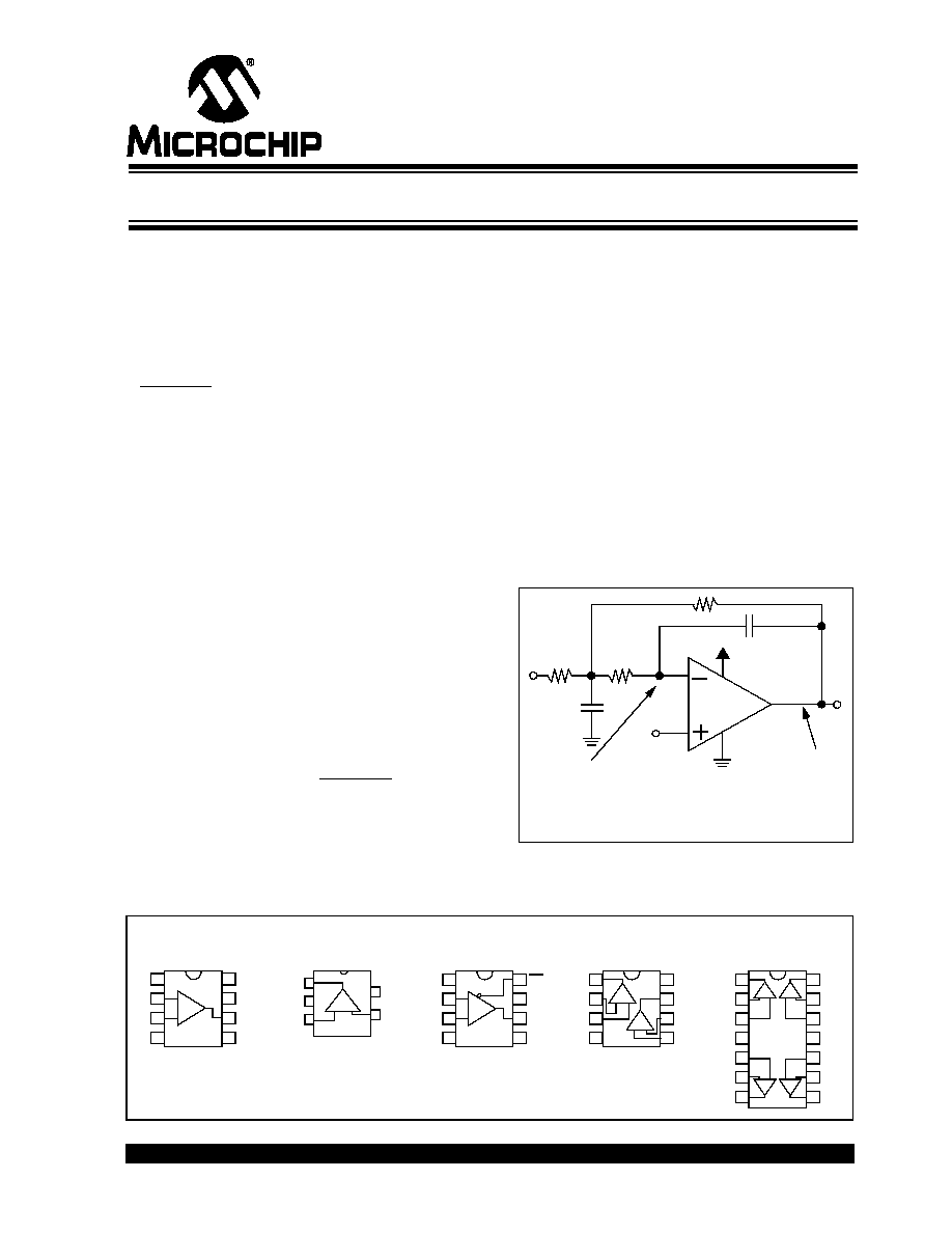
TYPICAL APPLICATION
PACKAGES
MCP60X
V
REF
V
IN
V
OUT
OUT
V
SS
V
DD
-IN
+IN
2nd Order Low Pass Filter
Low Input Bias
Current Over
Temperature
Rail-to-Rail
Output Swing
+IN
-IN
V
SS
1
2
3
4
NC
+INA
-INA
V
DD
-IND
+IND
1
2
3
4
V
SS
OUTD
OUTA
14
13
12
11
-INB
+INB
OUTB
5
6
7
+INA
-INA
V
SS
1
2
3
4
OUTA
+IN
-IN
V
SS
1
2
3
4
NC
V
DD
OUT
NC
CS
8
7
6
5
OUTB
-INB
+INB
V
DD
8
7
6
5
PDIP, SOIC, TSSOP
MCP601
MCP602
V
DD
OUT
PDIP, SOIC, TSSOP
MCP604
-
NC
NC
A
B
MCP603
8
7
6
5
+
+
-
+
-
-
+
A
+
-
+INC
-INC
OUTC
10
9
8
D
+
-
B
+
-
C
+
-
PDIP, SOIC, TSSOP
PDIP, SOIC, TSSOP
1
2
3
4
5
-
+
OUT
V
SS
+IN
V
DD
-IN
MCP601
SOT23-5
2.7V to 5.5V Single Supply CMOS Op Amps
MCP601/602/603/604
DS21314D-page 2
2000 Microchip Technology Inc.
1.0
ELECTRICAL
CHARACTERISTICS
1.1
Maximum Ratings*
V
DD
..................................................................................7.0V
All inputs and outputs w.r.t. ............. V
SS
-0.3V to V
DD
+0.3V
Difference Input voltage ....................................... |V
DD
- V
SS
|
Output Short Circuit Current ..................................continuous
Current at Input Pin .......................................................±2mA
Current at Output and Supply Pins .............................±30mA
Storage temperature .....................................-65∞C to +150∞C
Ambient temp. with power applied ................-55∞C to +125∞C
Soldering temperature of leads (10 seconds) ............. +300∞C
ESD Tolerance .................................3KV Human Body Model
*Notice: Stresses above those listed under "Maximum Ratings"
may cause permanent damage to the device. This is a stress rat-
ing only and functional operation of the device at those or any
other conditions above those indicated in the operational listings
of this specification is not implied. Exposure to maximum rating
conditions for extended periods may affect device reliability.
PIN FUNCTION TABLE
DC CHARACTERISTICS
NAME
FUNCTION
+IN, +INA, +INB, +INC, +IND
Non-inverting Input
Terminals
-IN, -INA, -INB, -INC, -IND
Inverting Input Terminals
V
DD
Positive Power Supply
V
SS
Negative Power Supply
OUT, OUTA, OUTB, OUTC, OUTD Output Terminals
CS
Chip Select
NC
No internal connection
to IC
Unless otherwise indicated, all limits are specified for V
DD
= +2.7V to +5.5V, V
SS
= GND, T
A
= 25 ∞C, V
CM
= V
DD
/2, R
L
= 100k
to
V
DD
/2, and V
OUT
~ V
DD
/2
PARAMETERS
SYMBOL
MIN.
TYP.
MAX.
UNITS
CONDITIONS
INPUT OFFSET VOLTAGE
Input Offset Voltage
V
OS
-2
+2
mV
Over Temperature
(1)
V
OS
-3
+3
mV
T
A
= -40∞C to +85∞C
Drift with Temperature
dV
OS
/dT
--
±2.5
--
µV/∞C
T
A
= -40∞C to +85∞C
Power Supply Rejection
PSRR
--
40
100
µV/V
for V
DD
= 2.7V to 5.5V
INPUT CURRENT AND IMPEDANCE
Input Bias Current
I
B
--
1
--
pA
Over Temperature
(2)
I
B
--
20
60
pA
T
A
= -40∞C to +85∞C
Input Offset Bias Current
I
OS
--
1
--
pA
Common Mode Input Impedance
Z
CM
--
10
13
||6
--
||pF
Differential Input Impedance
Z
DIFF
--
10
13
||3
--
||pF
COMMON MODE
Common-Mode Input Range
V
CM
V
SS
-0.3
--
V
DD
-1.2
V
Common-Mode Rejection Ratio
CMRR
75
90
--
dB
V
DD
= 5V,
V
CM
= -0.3 to 3.8V
OPEN LOOP GAIN
DC Open Loop Gain
A
OL
100
115
--
dB
R
L
= 25k
to V
DD
/2,
50mV < V
OUT
<
(V
DD
- 50 mV)
DC Open Loop Gain
A
OL
95
110
--
dB
R
L
= 5k
to V
DD
/2,
100mV < V
OUT
<
(V
DD
- 100mV)
OUTPUT
Low Level/High Level Output Swing
V
OL
, V
OH
V
SS
+ 0.015
--
V
DD
- 0.020
V
R
L
= 25k
to V
DD
/2
V
OL
, V
OH
V
SS
+ 0.045
--
V
DD
- 0.060
V
R
L
= 5k
to V
DD
/2
Linear Region Maximum Output
Voltage Swing
V
OUT
V
SS
+ 0.050
--
V
DD
- 0.050
V
R
L
= 25k
to V
DD
/2,
A
OL
100dB
V
OUT
V
SS
+ 0.100
--
V
DD
- 0.100
V
R
L
= 5k
to V
DD
/2,
A
OL
95dB
Output Short Circuit Current
I
SC
20
--
mA
V
OUT
= 2.5V,
V
DD
= 5V
POWER SUPPLY
Supply Voltage
V
DD
2.7
--
5.5
V
Quiescent Current Per Amp
I
Q
230
325
µA
I
L
= 0
Note 1: Max. and Min. specified for PDIP and SOIC packages only. Typical refers to all other packages
Note 2: Max. and Min. specified for PDIP, SOIC, and TSSOP packages only. Typical refers to all packages.

2000 Microchip Technology Inc.
DS21314D-page 3
MCP601/602/603/604
AC CHARACTERISTICS
SPECIFICATIONS FOR MCP603 CHIP SELECT FEATURE
TEMPERATURE SPECIFICATIONS
Unless otherwise indicated, all limits are specified for V
DD
= +2.7V to +5.5V, V
SS
= GND, T
A
= 25∞C, V
CM
= V
DD
/2, R
L
= 100k
to
V
DD
/2, and V
OUT
~ V
DD
/2
PARAMETERS
SYMBOL
MIN.
TYP.
MAX.
UNITS
CONDITIONS
Gain Bandwidth Product
GBWP
--
2.8
MHz
V
DD
= 5V
Phase Margin
m
--
50
--
degrees
C
L
= 50pF, V
DD
= 5V
Slew Rate
SR
--
2.3
--
V/
µs
G = +1V/V, V
DD
= 5V
Setting Time to 0.01%
--
4.5
--
µs
for
V
OUT
= 3.8V
STEP
,
C
L
= 50pF, V
DD
= 5V,
G = +1V/V
NOISE
Input Voltage Noise
e
n
--
7
--
µV
P-P
f = 0.1Hz to 10Hz
Input Voltage Noise Density
e
n
--
29
--
nV/
f = 1kHz
Input Current Noise Density
i
n
--
0.6
--
fA/
f = 1kHz
Unless otherwise indicated, all limits are specified for V
DD
= +2.7V to +5.5V, V
SS
= GND, T
A
= 25∞C, V
CM
= V
DD
/2, R
L
= 100k
to
V
DD
/2, and V
OUT
~ V
DD
/2
PARAMETERS
SYMBOL
MIN.
TYP.
MAX.
UNITS
CONDITIONS
CS LOW SPECIFICATIONS
CS Logic Threshold, Low
V
IL
V
SS
0.42 V
DD
0.2 V
DD
V
For entire V
DD
range
CS Input Current, Low
I
CSL
-1.0
--
--
µA
CS = 0.2V
DD
Amplifier Output Leakage, CS High
--
1
--
nA
CS HIGH SPECIFICATIONS
CS Logic Threshold, High
V
IH
0.8 V
DD
0.51 V
DD
V
DD
V
For entire V
DD
range
CS Input High, Shutdown CS Pin
Current
I
CSH
--
0.7
2.0
µA
CS = V
DD
CS Input High, Shutdown GND
Current
I
Q
--
0.7
2.0
µA
CS = V
DD
DYNAMIC SPECIFICATIONS
CS Low to Amplifier Output High
Turn-on Time
t
ON
--
3.1
10
µs
CS low
0.2V
DD
CS High to Amplifier Output High Z
t
OFF
--
100
--
ns
CS high
0.8V
DD
, No
Load
CS Threshold Hysteresis
--
0.3
--
V
Hz
Hz
Unless otherwise indicated, all limits are specified for V
DD
= +2.7V to +5.5V, V
SS
= GND
PARAMETERS
SYMBOL
MIN.
TYP.
MAX.
UNITS
CONDITIONS
TEMPERATURE RANGE
Specified Temperature Range
T
A
-40
--
+85
∞C
Operating Temperature Range
T
A
-40
--
+85
∞C
Storage Temperature Range
T
A
-65
--
+150
∞C
THERMAL PACKAGE RESISTANCE
Thermal Resistance, 5L-SOT23-5
JA
--
256
--
∞C/W
Thermal Resistance, 8L-PDIP
JA
--
85
--
∞C/W
Thermal Resistance, 8L-SOIC
JA
--
163
--
∞C/W
Thermal Resistance, 8L-TSSOP
JA
--
124
--
∞C/W
Thermal Resistance, 14L-PDIP
JA
--
70
--
∞C/W
Thermal Resistance, 14L-SOIC
JA
--
120
--
∞C/W
Thermal Resistance, 14L-TSSOP
JA
--
100
--
∞C/W
MCP601/602/603/604
DS21314D-page 4
2000 Microchip Technology Inc.
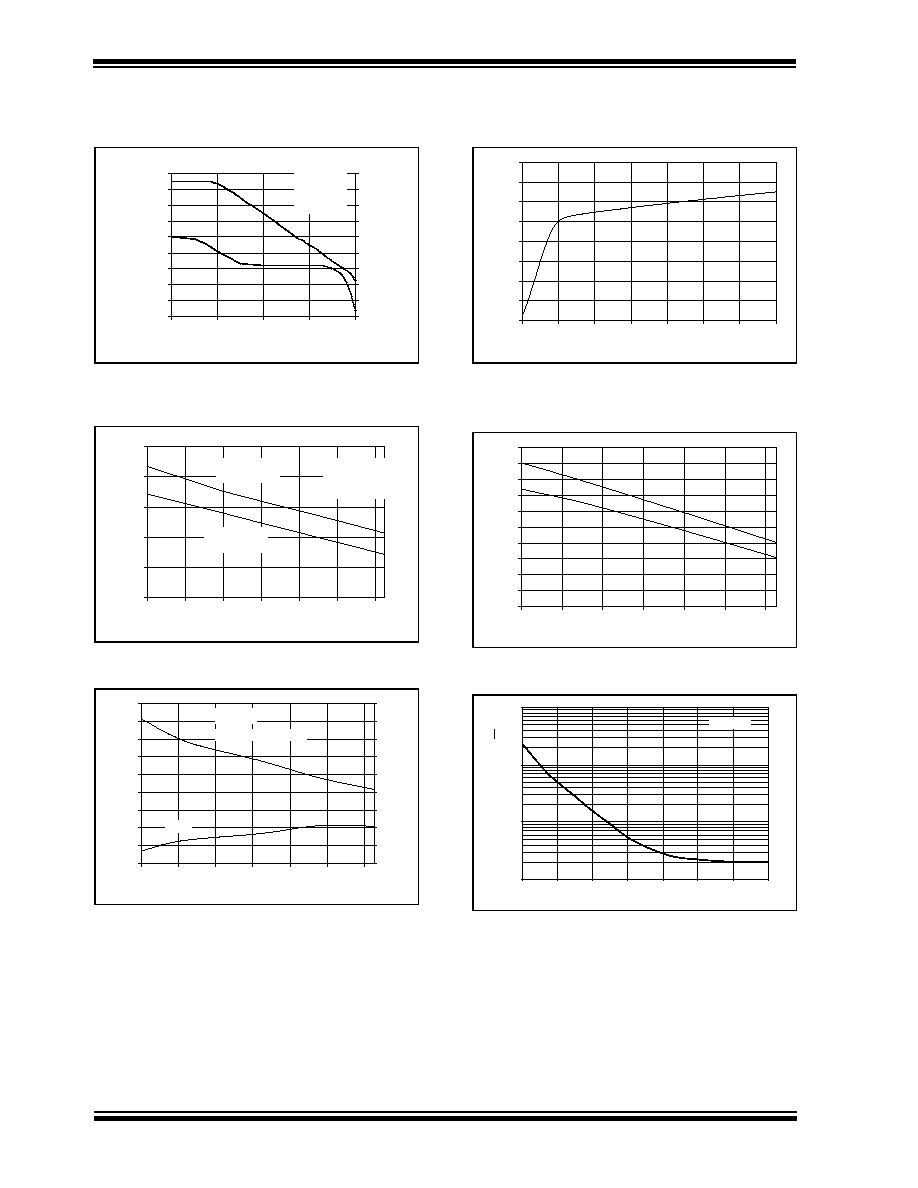
2.0
TYPICAL PERFORMANCE CURVES
Note: Unless otherwise indicated, V
DD
= +2.7V to +5.5V, T
A
= 25∞C, V
CM
= V
DD
/2, R
L
= 25k
to V
DD
/2 and V
OUT
~ V
DD
/2
FIGURE 2-1:
Open Loop Gain, Phase Margin vs.
Frequency
FIGURE 2-2:
Slew Rate vs. Temperature
FIGURE 2-3:
Gain Bandwidth Product vs.
Temperature
FIGURE 2-4:
Quiescent Current vs. Power Supply
FIGURE 2-5:
Quiescent Current vs. Temperature
FIGURE 2-6:
Input Voltage Noise Density vs.
Frequency
P
hase
Ma
rg
i
n
(
deg
ree
s
)
-60
-40
-20
0
20
40
60
80
100
120
0
10
1000
100000
10000000
Frequency (Hz)
Open Loop Gai
n
(dB
)
-250
-200
-150
-100
-50
0
50
100
150
200
C
L
= 50pF,
R
L
= 100k
V
DD
= 5V
Gain
Phase
0.1 10 1K 100K 10M
1
1.5
2
2.5
3
3.5
-40
-20
0
20
40
60
80
Temperature (∞C)
S
l
e
w
R
a
te
(
V
/µ
s)
High-to-Low
Transition
Low-to-High
Transition
C
L
=50pF,
R
L
=100k
,
V
DD
=5V
0
0.5
1
1.5
2
2.5
3
3.5
4
4.5
-40
-20
0
20
40
60
80
Temperature (∞C)
Gain Bandw
idt
h
Produc
t
(M
H
z
)
40
45
50
55
60
65
70
75
80
85
Phas
e M
a
rgin (degrees
)
Gain Bandwidth Product
Phase
C
L
= 55pF
100
120
140
160
180
200
220
240
260
2.0
2.5
3.0
3.5
4.0
4.5
5.0
5.5
Power Supply, V
DD
(V)
Quies
c
ent
C
u
rrent
per Am
plif
ier (
µ
A)
I
L
= 0
100
120
140
160
180
200
220
240
260
280
300
-40
-20
0
20
40
60
80
Temperature (∞C)
Quies
c
ent
C
u
rrent
per Am
plif
ier (µA)
V
DD
= 5.5V
V
DD
= 2.7V
I
L
= 0
0.1
1
10
100
1k
10k
100k
1M
10
100
1000
10000
Frequency (Hz)
I
n
p
u
t
V
o
l
t
ag
e Nois
e De
ns
it
y
(
n
V
/
Hz
)
R
L
= 10k
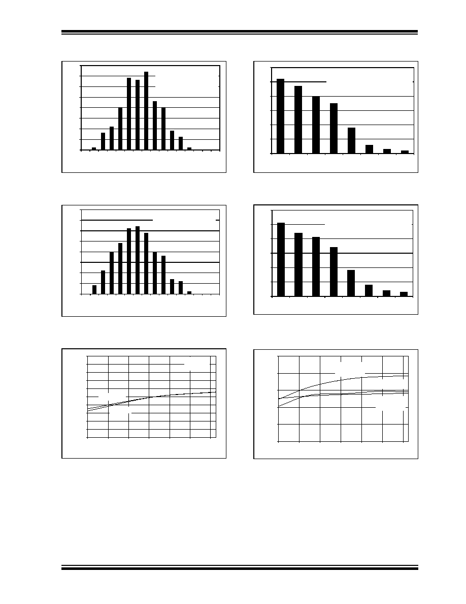
2000 Microchip Technology Inc.
DS21314D-page 5
MCP601/602/603/604
Note: Unless otherwise indicated, V
DD
= +2.7V to +5.5V, T
A
= 25∞C, V
CM
= V
DD
/2, R
L
= 25k
to V
DD
/2 and V
OUT
~ V
DD
/2
FIGURE 2-7:
Offset Voltage vs. Number of
Occurrences with V
DD
= 5.5V
FIGURE 2-8:
Offset Voltage vs. Number of
Occurrences with V
DD
= 2.7V.
FIGURE 2-9:
Normalized Offset Voltage vs. Temper-
ature with V
DD
= 2.7V
FIGURE 2-10: Offset Voltage Drift vs. Number of
Occurrences with V
DD
= 5.5V
FIGURE 2-11: Offset Voltage Drift vs. Number of
Occurrences with V
DD
= 2.7V
FIGURE 2-12: Common-Mode Rejection Ratio,
Power Supply Rejection Ratio vs. Temperature
0
5
10
15
20
25
30
35
40
-
1.75
-1
.5
0
-1
.2
5
-1
.0
0
-0
.7
5
-0.50
-
0.25
0.00
0.25
0.
50
0.
75
1.
00
1.
25
1.50
1.75
2.00
Offset Voltage (mV)
Nu
m
b
e
r
o
f
O
ccur
a
c
ne
s
-2
.
00
V
DD
= 5.5V
R
L
= 100k
Sample Size = 203 op amp
0
5
10
15
20
25
30
35
40
-1
.7
5
-1
.5
0
-1
.2
5
-1
.0
0
-0
.7
5
-0
.5
0
-0
.2
5
0.
0
0
0.
2
5
0.
5
0
0.
7
5
1.
0
0
1.
2
5
1.
5
0
1.
7
5
2.
0
0
Offset Voltage (mV)
N
u
m
b
e
r
of
O
c
cur
a
nce
s
-2
.0
0
V
DD
= 2.7V
R
L
= 100k
Sample Size = 203 op amp
-500
-400
-300
-200
-100
0
100
200
300
400
500
-40
-20
0
20
40
60
80
Temperature (∞C)
Of
f
s
et
Volt
age (µV)
V
DD
= 5.5V
V
DD
= 2.7V
R
L
= 100k
0
10
20
30
40
50
60
1
2
3
4
5
6
7
8
Change in Offset Voltage with Temperature (
µV/
∞
C)
N
u
m
b
e
r
of
O
c
c
u
r
a
nc
e
s
0
V
DD
= 5.5V
R
L
= 100k
Sample Size = 203
Temperature Range = -40∞C to +85
∞C
0
10
20
30
40
50
60
1
2
3
4
5
6
7
8
Change in Offset Voltage with Temperature (
µV/∞C)
Nu
m
b
er
o
f
O
cc
u
r
a
n
c
es
0
1
1
V
DD
= 2.7V
R
L
= 100k
Sample Size = 203
Temperature Range = -40∞C to +85
∞C
75
80
85
90
95
100
-40
-20
0
20
40
60
80
Temperature (∞ C)
C
o
m
m
on M
ode R
e
j
e
ct
i
on R
a
t
i
o,
P
o
w
e
r S
uppl
y R
e
j
e
ct
i
o
n
Ra
t
i
o
(
d
B)
CMRR
V
DD
= 2.7V
V
CM
= -0.3V to 1.5V
PSRR,
V
DD
= 2.7V to 5.5V
CMRR
V
DD
= 5.5V
V
CM
= -0.3V to 4.3V