600nA, Non-Unity Gain Rail-to-Rail Input/Output Op Amps
2002 Microchip Technology Inc.
21668A-page 1
M
MCP6141/2/3/4
Features
· Low Quiescent Current: 600 nA/Amplifier (typ.)
· Stable for gains of 10 V/V or higher
· Rail-to-Rail Input: -0.3V (min.) to V
DD
+ 0.3V (max.)
· Rail-to-Rail Output:
- V
SS
+10 mV (min.) to V
DD
-10 mV (max.)
· Gain Bandwidth Product: 100 kHz (typ.)
· Wide Supply Voltage Range: 1.4V to 5.5V (max.)
· Available in Single, Dual and Quad
· Chip Select (CS) with MCP6143
Applications
· Toll Booth Tags
· Wearable Products
· Temperature Measurement
· Battery-Powered
Available Tools
· Spice macro models (at www.microchip.com)
· FilterLab
®
Software (at www.microchip.com)
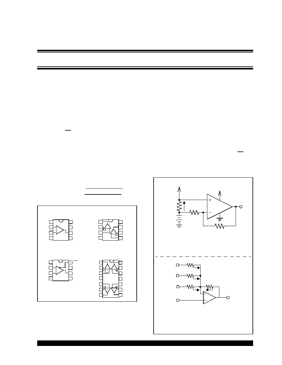
Package Types
Description
The MCP6141/2/3/4 family of non-unity gain stable
operational amplifiers (op amps) from Microchip
Technology, Inc. operate with a single supply voltage
as low as 1.4V, while drawing less than 1 µA (max.) of
quiescent current per amplifier. These devices are also
designed to support rail-to-rail input and output swing.
The MCP6141/2/3/4 op amps have a gain bandwidth
product of 100 kHz (typ.) and are stable for gains of
10 V/V or higher. This specification makes these
devices appropriate for battery-powered applications
where higher frequency responses from the amplifier
are required.
The MCP6141/2/3/4 family of op amps are offered in
single (MCP6141), single with a Chip Select (CS) fea-
ture (MCP6143), dual (MCP6142) and quad
(MCP6144) configurations.
Typical Applications
+IN
-IN
V
SS
V
DD
OUT
1
2
3
4
8
7
6
5
-
+
NC
NC
NC
+INA
-INA
V
SS
1
2
3
4
8
7
6
5
-
OUTA
+ -
+
A
B
V
DD
OUTB
-INB
+INB
+IN
-IN
V
SS
V
DD
OUT
1
2
3
4
8
7
6
5
-
+
NC
CS
NC
+INA1
-INA1
V
SS
1
2
3
4
14
13
12
11
-
OUTA
+ -
+
A
D
V
DD
OUTD
-IND
+IND
10
9
8
5
6
7
OUTB1
-INB
+INB
+INC
-INC
OUTC
+
-
B
C
-
+
MCP6141
PDIP, SOIC, MSOP
MCP6142
PDIP, SOIC, MSOP
MCP6143
PDIP, SOIC, MSOP
MCP6144
PDIP, SOIC, TSSOP
V
DD
1k
MCP614X
R
I
R
F
= 1 M
V
DD
I
DD
+1.4V
to
5.5V
V
SS
High Side Battery Current Sensor
V
REF
MCP614X
R
3
R
F
V
3
V
2
V
1
V
OUT
R
2
R
1
I
1
I
2
I
3
I
F
Summing Amplifier
G
n
1 R
F
1
R
1
------
1
R
2
------
1
R
3
------
+
+
+
10V/V
=
G
n
1
R
F
R
I
------
+
10V/V
=
100 k
600 nA, Non-Unity Gain Rail-to-Rail Input/Output Op Amps
MCP6141/2/3/4
21668A-page 2
2002 Microchip Technology Inc.
1.0
ELECTRICAL
CHARACTERISTICS
1.1
Maximum Ratings
V
DD
- V
SS
.........................................................................7.0V
All inputs and outputs........................ V
SS
-0.3V to V
DD
+0.3V
Difference Input voltage ....................................... |V
DD
- V
SS
|
Output Short Circuit Current ..................................continuous
Current at Input Pins ....................................................±2 mA
Current at Output and Supply Pins ............................±30 mA
Storage temperature .....................................-65°C to +150°C
Junction Temperature, T
J
............................................ +150°C
ESD protection on all pins (HBM:MM)
..................
4 kV:200 V
Notice: Stresses above those listed under "Maximum Rat-
ings" may cause permanent damage to the device. This is a
stress rating only and functional operation of the device at
those or any other conditions above those indicated in the
operational listings of this specification is not implied. Expo-
sure to maximum rating conditions for extended periods may
affect device reliability.
PIN FUNCTION TABLE
DC ELECTRICAL SPECIFICATIONS
Name
Function
+IN/+INA/+INB/+INC/+IND
Non-inverting Inputs
-IN/-INA/-INB/-INC/-IND
Inverting Inputs
V
DD
Positive Power Supply
V
SS
Negative Power Supply
OUT/OUTA/OUTB/OUTC/OUTD Outputs
CS
Chip Select
NC
No internal connection
Electrical Characteristics: Unless otherwise indicated, all limits are specified for V
DD
= +1.4V to +5.5V, V
SS
= GND, T
A
= 25°C,
V
CM
= V
DD
/2, R
L
= 1 M
to V
DD
/2, and V
OUT
~ V
DD
/2.
Parameters
Sym
Min
Typ
Max
Units
Conditions
Input Offset
V
CM
= V
SS
Input Offset Voltage
V
OS
-3.0
--
+3.0
mV
Drift with Temperature
V
OS
/
T
--
±1.5
--
µV/°C T
A
= -40°C to +85°C
Power Supply Rejection
PSRR
70
85
--
dB
Input Bias Current and Impedance
Input Bias Current
I
B
--
1.0
--
pA
Input Bias Current Over-Temperature
I
B
--
--
100
pA
T
A
= -40°C to +85°C
Input Offset Current
I
OS
--
1.0
--
pA
Common Mode Input Impedance
Z
CM
--
10
13
||6
--
||pF
Differential Input Impedance
Z
DIFF
--
10
13
||6
--
||pF
Common Mode
Common-Mode Input Range
VCMR
V
SS
-
0.3
--
V
DD
+ 0.3
V
Common-Mode Rejection Ratio
CMRR
62
80
--
dB
V
DD
= 5V,
V
CM
= -0.3V to 5.3V
60
75
--
dB
V
DD
= 5V,
V
CM
= 2.5V to 5.3V
60
80
--
dB
V
DD
= 5V,
V
CM
= -0.3V to 2.5V
Open Loop Gain
DC Open Loop Gain (large signal)
A
OL
95
115
--
dB
R
L
= 50 k
to V
DD
/2,
100 mV < V
OUT
<
(V
DD
-
100 mV)
Output
Maximum Output Voltage Swing
V
OL
, V
OH
V
SS
+ 10
--
V
DD
-
10
mV
R
L
= 50 k
to V
DD
/2
Output Short Circuit Current
I
O
--
21
--
mA
V
OUT
= 2.5V, V
DD
= 5 V
Power Supply
Supply Voltage
V
DD
1.4
--
5.5
V
Quiescent Current per amplifier
I
Q
0.3
0.6
1.0
µA
I
O
= 0
2002 Microchip Technology Inc.
21668A-page 3
MCP6141/2/3/4
AC ELECTRICAL SPECIFICATIONS
SPECIFICATIONS FOR MCP6143 CHIP SELECT FEATURE
TEMPERATURE SPECIFICATIONS
Electrical Characteristics: Unless otherwise indicated, all limits are specified for V
DD
= +5V, V
SS
= GND, T
A
= 25 °C,
V
CM
= V
DD
/2, R
L
= 1 M
to V
DD
/2, C
L
= 60 pF, and V
OUT
~ V
DD
/2.
Parameters
Sym
Min
Typ
Max
Units
Conditions
Gain Bandwidth Product
GBWP
--
100
--
kHz
Slew Rate
SR
--
24
--
V/ms
Phase Margin
PM
--
60
--
°
G = +10
Input Voltage Noise
E
n
--
5.0
--
µVp-p
f = 0.1 Hz to 10 Hz
Input Voltage Noise Density
e
n
--
170
--
nV/
Hz
f = 1 kHz
Input Current Noise Density
i
n
--
0.6
--
fA/
Hz
f = 1 kHz
Electrical Characteristics: Unless otherwise indicated, all limits are specified for V
DD
= +1.4V to +5.5V, V
SS
= GND, T
A
= 25 °C,
V
CM
= V
DD
/2, R
L
= 1 M
to V
DD
/2, C
L
= 60 pF, and V
OUT
~ V
DD
/2.
Parameters
Sym
Min
Typ
Max
Units
Conditions
CS Low Specifications
CS Logic Threshold, Low
V
IL
V
SS
--
V
SS
+ 0.3
V
For entire V
DD
range
CS Input Current, Low
I
CSL
--
5.0
--
pA
CS = V
SS
CS High Specifications
CS Logic Threshold, High
V
IH
V
DD
- 0.3
--
V
DD
V
For entire V
DD
range
CS Input Current, High
I
CSH
--
5.0
--
pA
CS = V
DD
CS Input High, GND Current
I
Q
--
20
--
pA
CS = V
DD
Amplifier Output Leakage, CS High
--
20
--
pA
CS = V
DD
Dynamic Specifications
CS Low to Amplifier Output High
Turn-on Time
t
ON
--
2.0
50
ms
CS low = V
SS
+ 0.3V, G = +1 V/V,
V
OUT
= 0.9 V
DD
/2
CS High to Amplifier Output High Z
t
OFF
--
10
--
µs
CS high = V
DD
- 0.3V, G = +1 V/V
V
OUT
= 0.1 V
DD
/2
Hysteresis
V
HYST
--
0.6
--
V
V
DD
= 5V
Electrical Characteristics: Unless otherwise indicated, all limits are specified for V
DD
= +1.4V to +5.5V, V
SS
= GND.
Parameters
Symbol
Min
Typ
Max
Units
Conditions
Temperature Ranges
Specified Temperature Range
T
A
-40
--
+85
°C
Operating Temperature Range
T
A
-40
--
+125
°C
Note 1
Storage Temperature Range
T
A
-65
--
+150
°C
Thermal Package Resistances
Thermal Resistance, 8L-PDIP
JA
--
85
--
°C/W
Thermal Resistance, 8L-SOIC
JA
--
163
--
°C/W
Thermal Resistance, 8L-MSOP
JA
--
206
--
°C/W
Thermal Resistance, 14L-PDIP
JA
--
70
--
°C/W
Thermal Resistance, 14L-SOIC
JA
--
108
--
°C/W
Thermal Resistance, 14L-TSSOP
JA
--
100
--
°C/W
Note 1: The MCP6141/2/3/4 family of op amps operates over this extended range, but with reduced performance.
MCP6141/2/3/4
21668A-page 4
2002 Microchip Technology Inc.
2.0
TYPICAL PERFORMANCE CURVES
Note: Unless otherwise indicated, V
DD
= +5V, V
SS
= GND, T
A
= 25°C, V
CM
= V
DD
/2, R
L
= 1 M
to V
DD
/2, C
L
= 60 pF
,
and V
OUT
~ V
DD
/2.
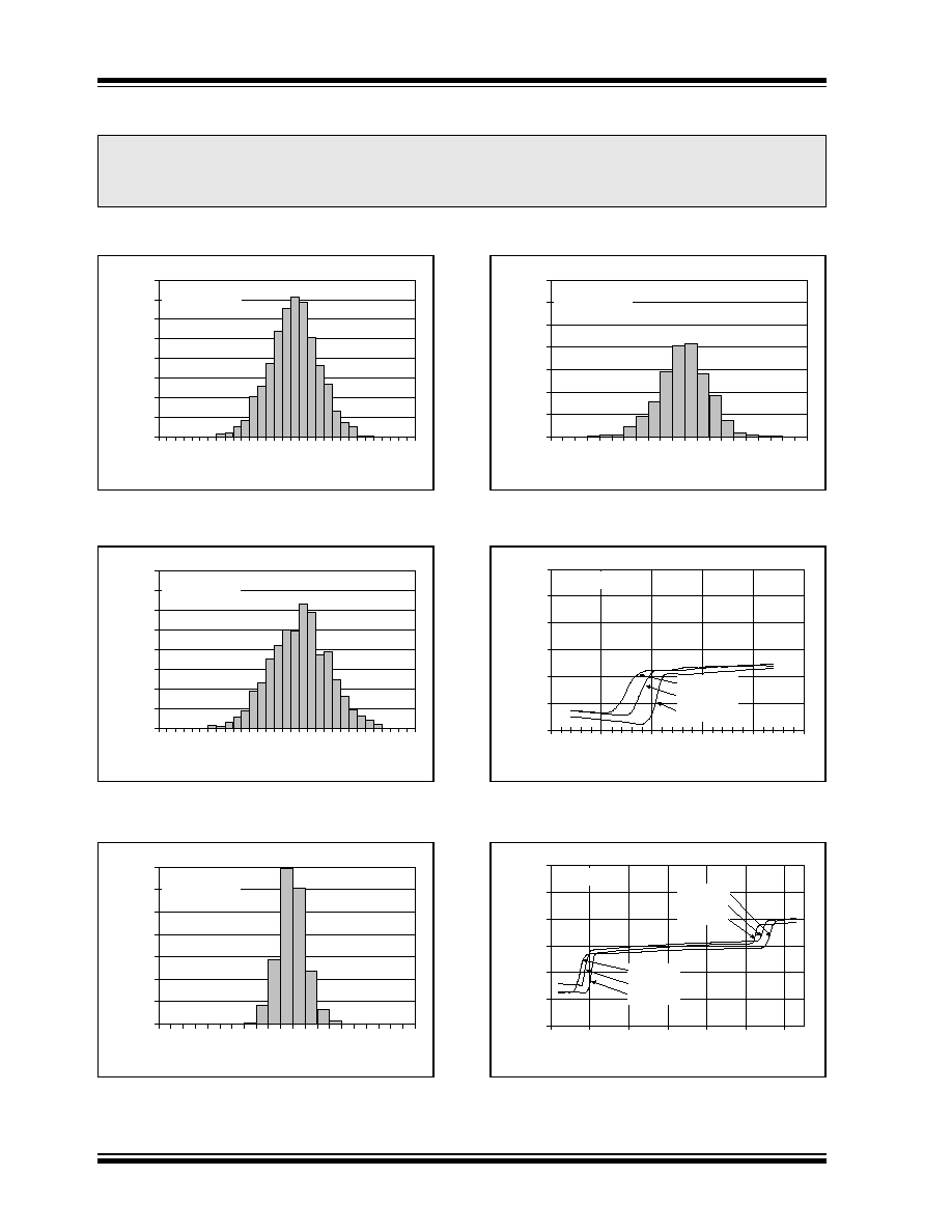
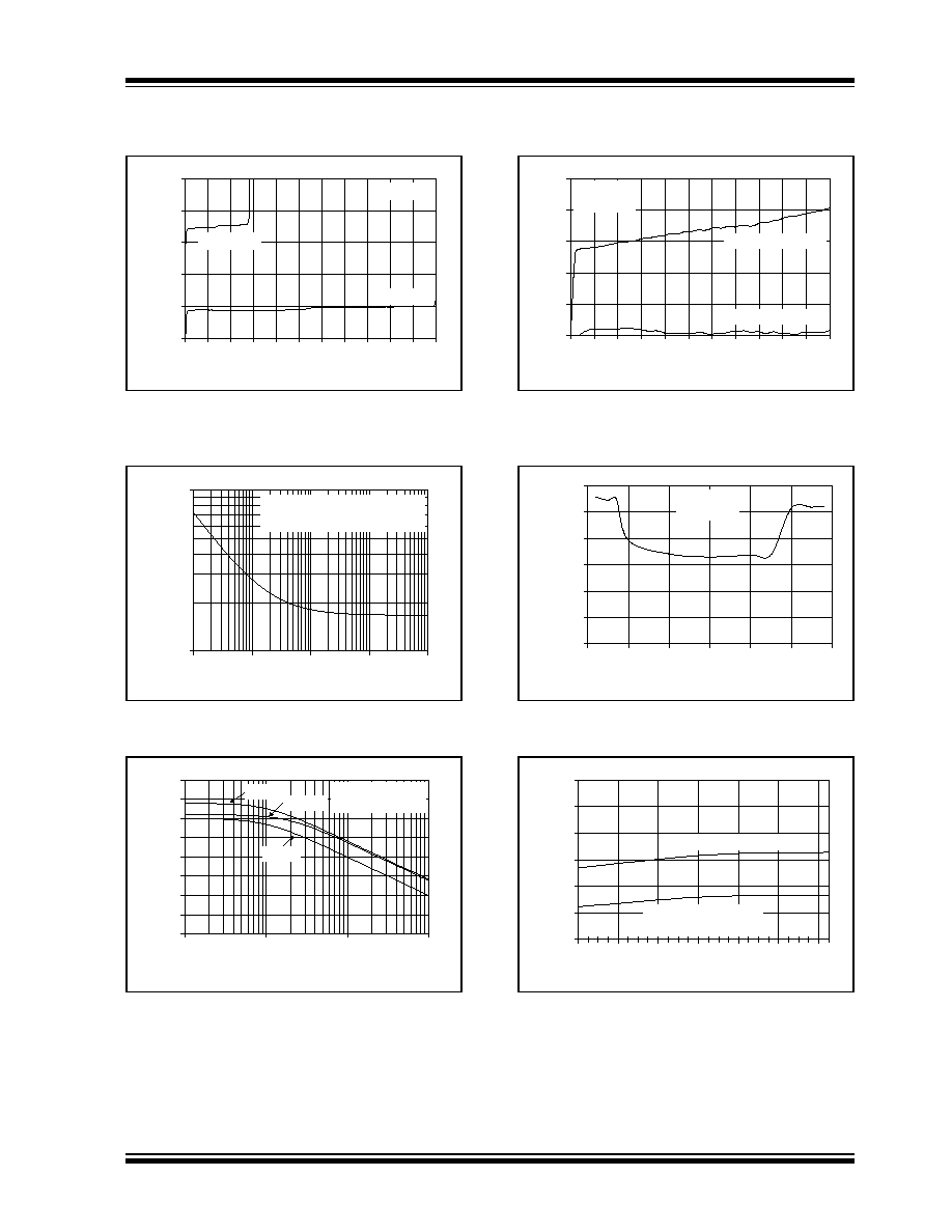
FIGURE 2-1:
Histogram of Input Offset
Voltage with V
DD
= 5.5V.
FIGURE 2-2:
Histogram of Input Offset
Voltage with V
DD
= 1.4V.
FIGURE 2-3:
Histogram of Input Offset
Voltage Drift with V
DD
= 5.5V.
FIGURE 2-4:
Histogram of Input Offset
Voltage Drift with V
DD
= 1.4V.
FIGURE 2-5:
Input Offset Voltage vs.
Common Mode Input Voltage vs. Temperature
with V
DD
= 1.4V.
FIGURE 2-6:
Input Offset Voltage vs.
Common Mode Input Voltage vs. Temperature
with V
DD
= 5.5V.
Note:
The graphs and tables provided following this note are a statistical summary based on a limited number of
samples and are provided for informational purposes only. The performance characteristics listed herein
are not tested or guaranteed. In some graphs or tables, the data presented may be outside the specified
operating range (e.g., outside specified power supply range) and therefore outside the warranted range.
0%
2%
4%
6%
8%
10%
12%
14%
16%
-3
-2
-1
0
1
2
3
Input Offset Voltage (mV)
Percentage of Occurrences
1200 Samples
V
DD
= 5.5 V
0%
2%
4%
6%
8%
10%
12%
14%
16%
-3
-2
-1
0
1
2
3
Input Offset Voltage (mV)
Percentage of Occurrences
1200 Samples
V
DD
= 1.4 V
0%
5%
10%
15%
20%
25%
30%
35%
-10
-5
0
5
10
Input Offset Voltage Drift (µV/°C)
Percentage of Occurrences
1200 Samples
V
DD
= 5.5 V
0%
5%
10%
15%
20%
25%
30%
35%
-10
-5
0
5
10
Input Offset Voltage Drift (µV/°C)
Percentage of Occurrences
1200 Samples
V
DD
= 1.4 V
-600
-400
-200
0
200
400
600
-0.5
0.0
0.5
1.0
1.5
2.0
Common Mode Input Voltage (V)
Input Offset Voltage (µV)
V
DD
= 1.4 V
T
A
= +85°C
T
A
= +25°C
T
A
= -40°C
-600
-400
-200
0
200
400
600
-0.5
0.5
1.5
2.5
3.5
4.5
5.5
Common Mode Input Voltage (V)
Input Offset Voltage (µV)
V
DD
= 5.5 V
T
A
= +85°C
T
A
= +25°C
T
A
= -40°C
T
A
= +85°C
T
A
= +25°C
T
A
= -40°C
2002 Microchip Technology Inc.
21668A-page 5
MCP6141/2/3/4
Note: Unless otherwise indicated, V
DD
= +5V, V
SS
= GND, T
A
= 25°C, V
CM
= V
DD
/2, R
L
= 1 M
to V
DD
/2, C
L
= 60 pF
,
and V
OUT
~ V
DD
/2.
FIGURE 2-7:
Input Offset Voltage vs.
Output Voltage vs. Power Supply Voltage.
FIGURE 2-8:
Input Noise Voltage Density
vs. Frequency.
FIGURE 2-9:
Common Mode Rejection
Ratio, Power Supply Rejection Ratio vs.
Frequency.
FIGURE 2-10:
Input Bias, Offset Currents
vs. Common Mode Input Voltage with
Temperature = 85°C.
FIGURE 2-11:
Input Noise Voltage Density
vs. Common Mode Input Voltage.
FIGURE 2-12:
Common Mode Rejection
Ratio, Power Supply Rejection Ratio vs. Ambient
Temperature.
250
300
350
400
450
500
0.0 0.5 1.0 1.5 2.0 2.5 3.0 3.5 4.0 4.5 5.0 5.5
Output Voltage (V)
Input Offset Voltage (µV)
V
DD
= 1.4 V
R
L
= 50 k
V
DD
= 5.5 V
100
1,000
0.1
1
10
100
1000
Frequency (Hz)
Input Noise Voltage Density
(nV/
Hz)
E
ni
= 4.7 µV
P-P
, f = 0.1 to 10 Hz
e
ni
= 167 nV/ Hz, f = 1 kHz
20
30
40
50
60
70
80
90
100
1
10
100
1000
Frequency (Hz)
CMRR, PSRR (dB)
PSRR-
CMRR
PSRR+
V
DD
= 5.0 V
Referred to Input
10
100
0
10
20
30
40
50
0.0 0.5 1.0 1.5 2.0 2.5 3.0 3.5 4.0 4.5 5.0 5.5
Common Mode Input Voltage (V)
Input Bias, Offset Currents (pA)
Input Bias Current
Input Offset Current
T
A
= 85°C
V
DD
= 5.5 V
0
50
100
150
200
250
300
-0.5
0.5
1.5
2.5
3.5
4.5
5.5
Common Mode Input Voltage (V)
Input Noise Voltage Density
(nV/
Hz)
f = 1 kHz
V
DD
= 5.0 V
70
75
80
85
90
95
100
-40
-20
0
20
40
60
80
Ambient Temperature (°C)
CMRR, PSRR (dB)
PSRR (V
CM
= V
SS
)
CMRR (V
DD
= 5.0 V,
V
CM
= -0.3 V to +5.3 V)
Document Outline