 | ÐлекÑÑоннÑй компоненÑ: MCP6281 | СкаÑаÑÑ:  PDF PDF  ZIP ZIP |
Äîêóìåíòàöèÿ è îïèñàíèÿ www.docs.chipfind.ru
2004 Microchip Technology Inc.
DS21811D-page 1
MCP6281/2/3/4/5
Features
· Gain Bandwidth Product: 5 MHz (typ.)
· Supply Current: I
Q
= 450 µA (typ.)
· Supply Voltage: 2.2V to 5.5V
· Rail-to-Rail Input/Output
· Extended Temperature Range: -40°C to +125°C
· Available in Single, Dual and Quad Packages
· Single with Chip Select (CS) (MCP6283)
· Dual with Chip Select (CS) (MCP6285)
Applications
· Automotive
· Portable Equipment
· Photodiode Amplifier
· Analog Filters
· Notebooks and PDAs
· Battery-Powered Systems
Available Tools
· SPICE Macro Model (at www.microchip.com)
· FilterLab
®
Software (at www.microchip.com)
Description
The Microchip Technology Inc. MCP6281/2/3/4/5
family of operational amplifiers (op amps) provide wide
bandwidth for the current. This family has a 5 MHz
Gain Bandwidth Product (GBWP) and a 65° phase
margin. This family also operates from a single supply
voltage as low as 2.2V, while drawing 450 µA (typ.)
quiescent current. Additionally, the MCP6281/2/3/4/5
supports rail-to-rail input and output swing, with a
common mode input voltage range of V
DD
+ 300 mV to
V
SS
300 mV. This family of operational amplifiers is
designed with Microchip's advanced CMOS process.
The MCP6285 has a Chip Select (CS) input for dual op
amps in an 8-pin package. This device is manufactured
by cascading the two op amps (the output of op amp A
connected to the non-inverting input of op amp B). The
CS input puts the device in Low-power mode.
The MCP6281/2/3/4/5 family operates over the
Extended Temperature Range of -40°C to +125°C. It
also has a power supply range of 2.2V to 5.5V.
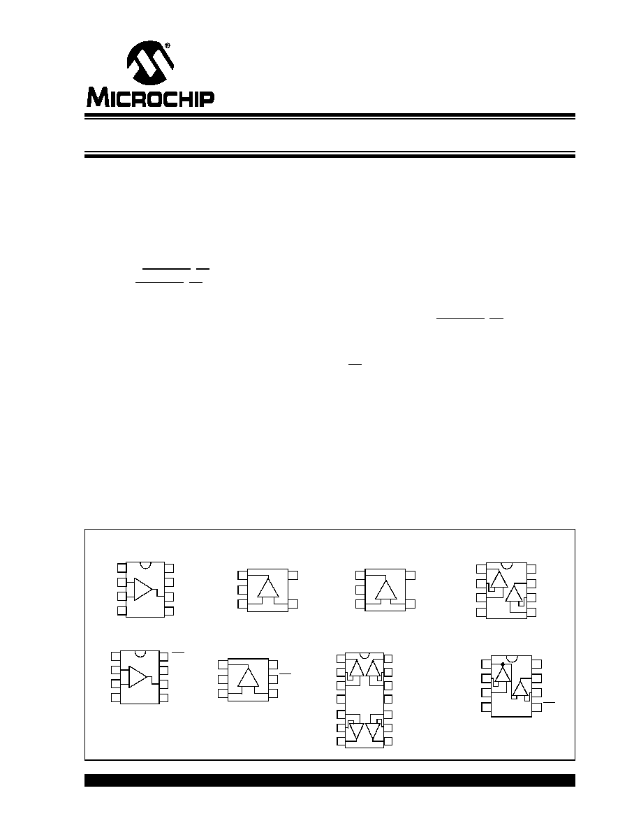
Package Types
V
IN
_
MCP6281
V
DD
1
2
3
4
8
7
6
5
-
+
NC
NC
NC
V
IN
+
V
SS
MCP6282
PDIP, SOIC, MSOP
MCP6284
1
2
3
4
14
13
12
11
-
+ -
+
10
9
8
5
6
7
+
-
-
+
PDIP, SOIC, TSSOP
1
2
3
4
8
7
6
5
-
+ -
+
V
OUT
MCP6283
1
2
3
4
8
7
6
5
-
+
V
INA
_
V
INA
+
V
SS
V
OUTA
V
OUTB
V
DD
V
INB
_
V
INB
+
V
SS
V
IN
+
V
IN
_
NC
CS
V
DD
V
OUT
NC
V
OUTA
V
INA
_
V
INA
+
V
DD
V
SS
V
OUTB
V
INB
_
V
INB
+
V
OUTC
V
INC
_
V
INC
+
V
OUTD
V
IND
_
V
IND
+
PDIP, SOIC, MSOP
PDIP, SOIC, MSOP
MCP6285
PDIP, SOIC, MSOP
1
2
3
4
8
7
6
5
+ -
V
INA
_
V
INA
+
V
SS
V
OUTA
/V
INB
+
V
OUTB
V
DD
V
INB
_
CS
- +
MCP6281
SOT-23-5
4
1
2
3
-
+
5 V
DD
V
IN
V
OUT
V
SS
V
IN
+
MCP6281R
SOT-23-5
4
1
2
3
-
+
5 V
SS
V
IN
V
OUT
V
DD
V
IN
+
MCP6283
SOT-23-6
4
1
2
3
-
+
6
5
V
SS
V
IN
+
V
OUT
CS
V
DD
V
IN
_
450 µA, 5 MHz Rail-to-Rail Op Amp
MCP6281/2/3/4/5
DS21811D-page 2
2004 Microchip Technology Inc.
1.0
ELECTRICAL
CHARACTERISTICS
Absolute Maximum Ratings
V
DD
V
SS
........................................................................7.0V
All Inputs and Outputs ................... V
SS
0.3V to V
DD
+ 0.3V
Difference Input Voltage ...................................... |V
DD
V
SS
|
Output Short Circuit Current ................................. Continuous
Current at Input Pins ....................................................±2 mA
Current at Output and Supply Pins ............................±30 mA
Storage Temperature.....................................-65°C to +150°C
Junction Temperature (T
J
) . .........................................+150°C
ESD Protection On All Pins (HBM;MM)
................
4 kV;400V
Notice: Stresses above those listed under "Maximum Rat-
ings" may cause permanent damage to the device. This is a
stress rating only and functional operation of the device at
those or any other conditions above those indicated in the
operational listings of this specification is not implied. Expo-
sure to maximum rating conditions for extended periods may
affect device reliability.
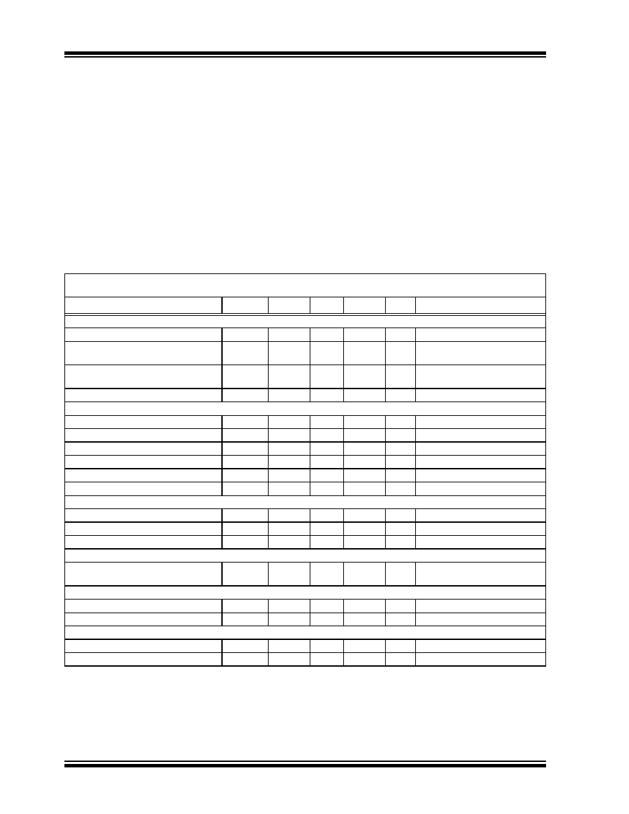
DC ELECTRICAL SPECIFICATIONS
Electrical Characteristics: Unless otherwise indicated, T
A
= +25°C, V
DD
= +2.2V to +5.5V, V
SS
= GND,
V
CM
= V
DD
/2, R
L
= 10 k
to V
DD
/2 and V
OUT
V
DD
/2.
Parameters
Sym
Min
Typ
Max
Units
Conditions
Input Offset
Input Offset Voltage
V
OS
-3.0
--
+3.0
mV
V
CM
= V
SS
(Note 1)
Input Offset Voltage
(Extended Temperature)
V
OS
-5.0
--
+5.0
mV
T
A
= -40°C to +125°C,
V
CM
= V
SS
(Note 1)
Input Offset Temperature Drift
V
OS
/
T
A
--
±1.7
--
µV/°C T
A
= -40°C to +125°C,
V
CM
= V
SS
(Note 1)
Power Supply Rejection Ratio
PSRR
70
90
--
dB
V
CM
= V
SS
(Note 1)
Input Bias, Input Offset Current and Impedance
Input Bias Current
I
B
--
±1.0
--
pA
Note 2
At Temperature
I
B
--
50
200
pA
T
A
= +85°C (Note 2)
At Temperature
I
B
--
2
5
nA
T
A
= +125°C (Note 2)
Input Offset Current
I
OS
--
±1.0
--
pA
Note 3
Common Mode Input Impedance
Z
CM
--
10
13
||6
--
||pF
Note 3
Differential Input Impedance
Z
DIFF
--
10
13
||3
--
||pF
Note 3
Common Mode (Note 4)
Common Mode Input Range
V
CMR
V
SS
-
0.3
--
V
DD
+ 0.3
V
Common Mode Rejection Ratio
CMRR
70
85
--
dB
V
CM
= -0.3V to 2.5V, V
DD
= 5V
Common Mode Rejection Ratio
CMRR
65
80
--
dB
V
CM
= -0.3V to 5.3V, V
DD
= 5V
Open-Loop Gain
DC Open-Loop Gain (Large Signal)
A
OL
90
110
--
dB
V
OUT
= 0.2V to V
DD
0.2V,
V
CM
= V
SS
(Note 1)
Output
Maximum Output Voltage Swing
V
OL
, V
OH
V
SS
+ 15
--
V
DD
15
mV
Output Short Circuit Current
I
SC
--
±25
--
mA
Power Supply
Supply Voltage
V
DD
2.2
--
5.5
V
Quiescent Current per Amplifier
I
Q
300
450
570
µA
I
O
= 0
Note
1:
The MCP6285's V
CM
for op amp B (pins V
OUTA
/V
INB
+ and V
INB
) is V
SS
+ 100 mV.
2:
The current at the MCP6285's V
INB
pin is specified by I
B
only.
3:
This specification does not apply to the MCP6285's V
OUTA
/V
INB
+ pin.
4:
The MCP6285's V
INB
pin (op amp B) has a common mode range (V
CMR
) of V
SS
+ 100 mV to V
DD
100 mV.
The MCP6285's V
OUTA
/V
INB
+ pin (op amp B) has a voltage range specified by V
OH
and V
OL
.
2004 Microchip Technology Inc.
DS21811D-page 3
MCP6281/2/3/4/5
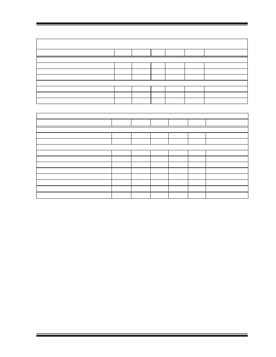
AC ELECTRICAL SPECIFICATIONS
TEMPERATURE SPECIFICATIONS
Electrical Characteristics: Unless otherwise indicated, T
A
= +25°C, V
DD
= +2.2V to +5.5V, V
SS
= GND,
V
CM
= V
DD
/2, V
OUT
V
DD
/2, R
L
= 10 k
to V
DD
/2 and C
L
= 60 pF.
Parameters
Sym
Min
Typ
Max
Units
Conditions
AC Response
Gain Bandwidth Product
GBWP
--
5.0
--
MHz
Phase Margin at Unity-Gain
PM
--
65
--
°
Slew Rate
SR
--
2.5
--
V/µs
Noise
Input Noise Voltage
E
ni
--
3.5
--
µV
P-P
f = 0.1 Hz to 10 Hz
Input Noise Voltage Density
e
ni
--
16
--
nV/
Hz
f = 1 kHz
Input Noise Current Density
i
ni
--
3
--
fA/
Hz
f = 1 kHz
Electrical Characteristics: Unless otherwise indicated, V
DD
= +2.2V to +5.5V and V
SS
= GND.
Parameters
Sym
Min
Typ
Max
Units
Conditions
Temperature Ranges
Operating Temperature Range
T
A
-40
--
+125
°C
Note
Storage Temperature Range
T
A
-65
--
+150
°C
Thermal Package Resistances
Thermal Resistance, 5L-SOT-23
JA
--
256
--
°C/W
Thermal Resistance, 6L-SOT-23
JA
--
230
--
°C/W
Thermal Resistance, 8L-PDIP
JA
--
85
--
°C/W
Thermal Resistance, 8L-SOIC
JA
--
163
--
°C/W
Thermal Resistance, 8L-MSOP
JA
--
206
--
°C/W
Thermal Resistance, 14L-PDIP
JA
--
70
--
°C/W
Thermal Resistance, 14L-SOIC
JA
--
120
--
°C/W
Thermal Resistance, 14L-TSSOP
JA
--
100
--
°C/W
Note:
The Junction Temperature (T
J
) must not exceed the Absolute Maximum specification of +150°C.
MCP6281/2/3/4/5
DS21811D-page 4
2004 Microchip Technology Inc.
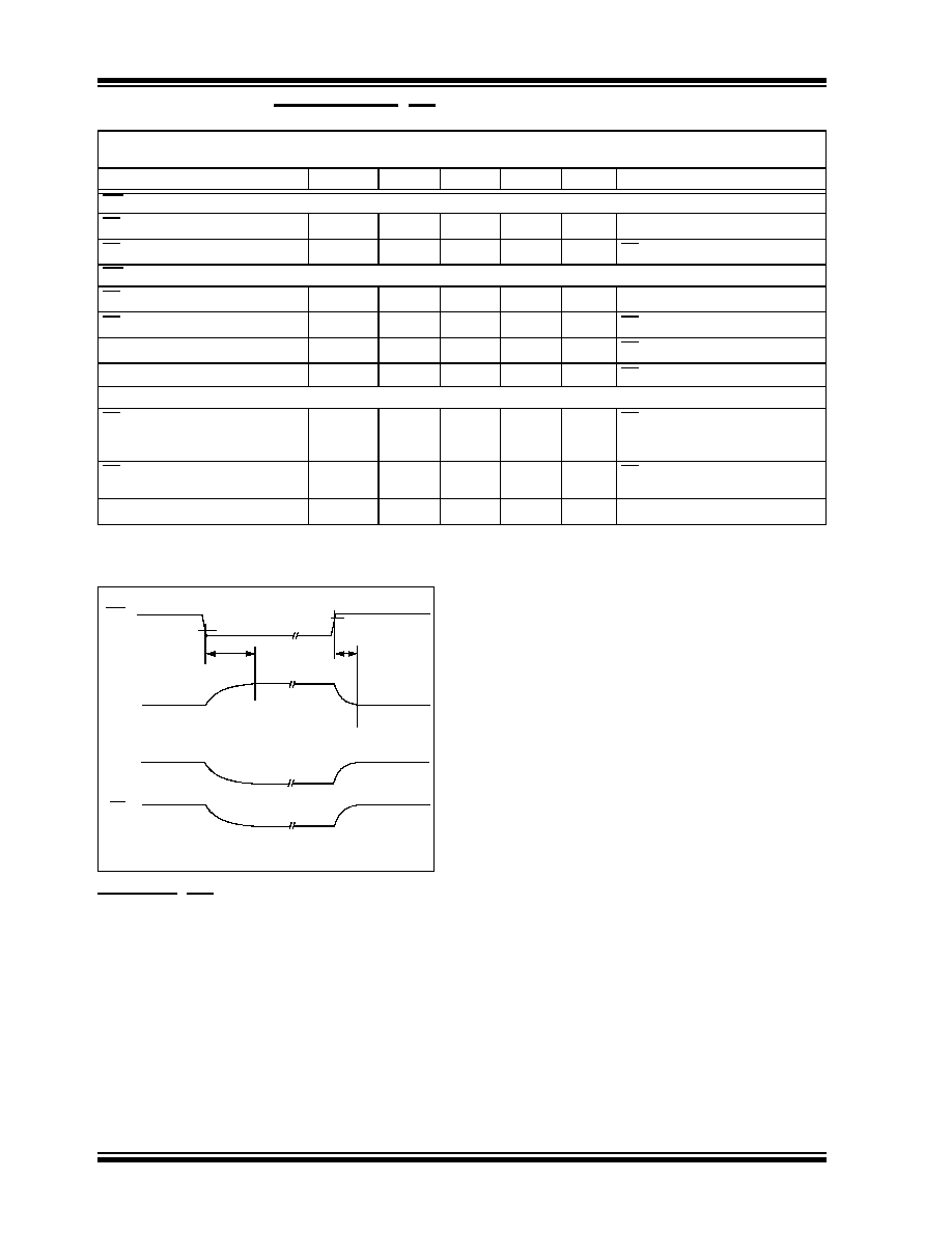
MCP6283/MCP6285 CHIP SELECT (CS) SPECIFICATIONS
FIGURE 1-1:
Timing Diagram for the
Chip Select (CS) pin on the MCP6283 and
MCP6285.
Electrical Characteristics: Unless otherwise indicated, T
A
= +25°C, V
DD
= +2.2V to +5.5V, V
SS
= GND,
V
CM
= V
DD
/2, V
OUT
V
DD
/2, R
L
= 10 k
to V
DD
/2 and C
L
= 60 pF.
Parameters
Sym
Min
Typ
Max
Units
Conditions
CS Low Specifications
CS Logic Threshold, Low
V
IL
V
SS
--
0.2 V
DD
V
CS Input Current, Low
I
CSL
--
0.01
--
µA
CS = V
SS
CS High Specifications
CS Logic Threshold, High
V
IH
0.8 V
DD
--
V
DD
V
CS Input Current, High
I
CSH
--
0.7
2
µA
CS = V
DD
GND Current per Amplifier
I
SS
--
-0.7
--
µA
CS = V
DD
Amplifier Output Leakage
--
--
0.01
--
µA
CS = V
DD
Dynamic Specifications (Note 1)
CS Low to Valid Amplifier
Output, Turn-on Time
t
ON
--
4
10
µs
CS Low
0.2 V
DD
, G = +1 V/V,
V
IN
= V
DD
/2, V
OUT
= 0.9 V
DD
/2,
V
DD
= 5.0V
CS High to Amplifier Output High-Z
t
OFF
--
0.01
--
µs
CS High
0.8 V
DD
, G = +1 V/V,
V
IN
= V
DD
/2, V
OUT
= 0.1 V
DD
/2
Hysteresis
V
HYST
--
0.6
--
V
V
DD
= 5V
Note
1:
The input condition (V
IN
) specified applies to both op amp A and B of the MCP6285. The dynamic specification is tested
at the output of op amp B (V
OUTB
).
V
IL
Hi-Z
t
ON
V
IH
CS
t
OFF
V
OUT
-0.7 µA (typ.)
Hi-Z
I
SS
I
CS
0.7 µA (typ.)
0.7 µA (typ.)
-0.7 µA (typ.)
-450 µA (typ.)
10 nA (typ.)
2004 Microchip Technology Inc.
DS21811D-page 5
MCP6281/2/3/4/5
2.0
TYPICAL PERFORMANCE CURVES
Note: Unless otherwise indicated, T
A
= +25°C, V
DD
= +2.2V to +5.5V, V
SS
= GND, V
CM
= V
DD
/2, V
OUT
V
DD
/2,
R
L
= 10 k
to V
DD
/2 and C
L
= 60 pF.
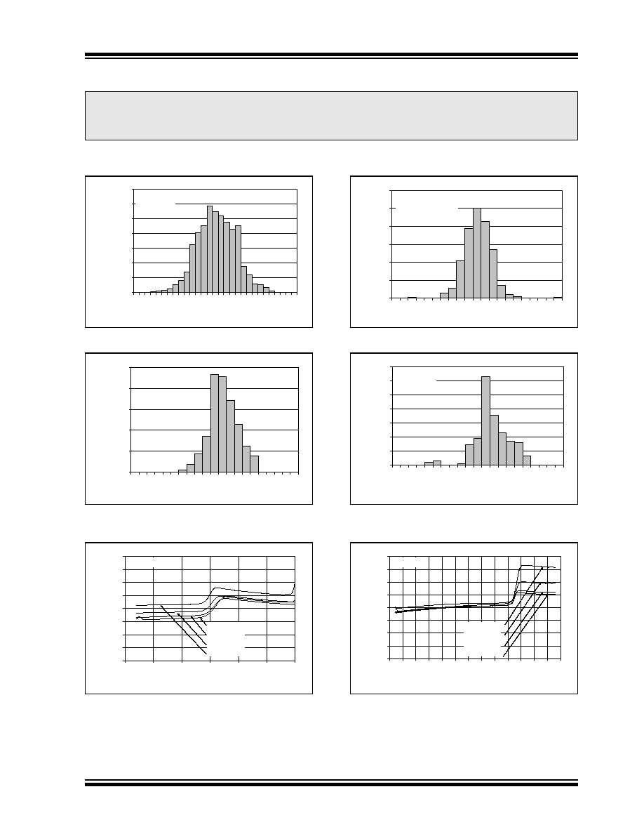
FIGURE 2-1:
Input Offset Voltage.
FIGURE 2-2:
Input Bias Current at
T
A
= +85 °C.
FIGURE 2-3:
Input Offset Voltage vs.
Common Mode Input Voltage at V
DD
= 2.2V.
FIGURE 2-4:
Input Offset Voltage Drift.
FIGURE 2-5:
Input Bias Current at
T
A
= +125 °C.
FIGURE 2-6:
Input Offset Voltage vs.
Common Mode Input Voltage at V
DD
= 5.5V.
Note:
The graphs and tables provided following this note are a statistical summary based on a limited number of
samples and are provided for informational purposes only. The performance characteristics listed herein
are not tested or guaranteed. In some graphs or tables, the data presented may be outside the specified
operating range (e.g., outside specified power supply range) and therefore outside the warranted range.
0%
2%
4%
6%
8%
10%
12%
14%
-2.
8
-2.
4
-2.
0
-1.
6
-1.
2
-0.
8
-0.
4
0.
0
0.
4
0.
8
1.
2
1.
6
2.
0
2.
4
2.
8
Input Offset Voltage (mV)
P
e
r
centage of Occur
r
e
nces
832 Samples
V
CM
= V
SS
0%
5%
10%
15%
20%
25%
0
10
20
30
40
50
60
70
80
90
100
Input Bias Current (pA)
Per
c
enta
ge of
O
c
cur
r
e
nce
s
210 Samples
T
A
= +85°C
-100
-50
0
50
100
150
200
250
300
-0.5
0.0
0.5
1.0
1.5
2.0
2.5
Common Mode Input Voltage (V)
Input
O
ffs
et Vo
ltag
e (
µ
V)
V
DD
= 2.2V
T
A
= +125°C
T
A
= +85°C
T
A
= +25°C
T
A
= -40°C
0%
5%
10%
15%
20%
25%
30%
-10
-8
-6
-4
-2
0
2
4
6
8
10
Input Offset Voltage Drift (µV/°C)
P
e
r
centage of Occur
r
e
nces
832 Samples
V
CM
= V
SS
T
A
= -40°C to +125°C
0%
5%
10%
15%
20%
25%
30%
35%
0
200
400
800
1
200
1
600
2
000
2
400
2
800
3
200
3
600
Input Bias Current (pA)
Per
c
enta
ge of O
c
cu
r
r
e
nc
e
s
210 Samples
T
A
= +125°C
-100
-50
0
50
100
150
200
250
300
-0
.
5
0.
0
0.
5
1.
0
1.
5
2.
0
2.
5
3.
0
3.
5
4.
0
4.
5
5.
0
5.
5
6.
0
Common Mode Input Voltage (V)
I
nput
O
ffse
t
Vol
t
ag
e (µ
V)
V
DD
= 5.5V
T
A
= +125°C
T
A
= +85°C
T
A
= +25°C
T
A
= -40°C
Document Outline
- 1.0 Electrical Characteristics
- 2.0 Typical Performance Curves
- Figure 2-1: Input Offset Voltage.
- Figure 2-2: Input Bias Current at TA = +85 °C.
- Figure 2-3: Input Offset Voltage vs. Common Mode Input Voltage at VDD = 2.2V.
- Figure 2-4: Input Offset Voltage Drift.
- Figure 2-5: Input Bias Current at TA = +125 °C.
- Figure 2-6: Input Offset Voltage vs. Common Mode Input Voltage at VDD = 5.5V.
- Figure 2-7: Input Offset Voltage vs. Output Voltage.
- Figure 2-8: CMRR, PSRR vs. Frequency.
- Figure 2-9: Input Bias, Offset Currents vs. Common Mode Input Voltage at TA = +85°C.
- Figure 2-10: Input Bias, Input Offset Currents vs. Ambient Temperature.
- Figure 2-11: CMRR, PSRR vs. Ambient Temperature.
- Figure 2-12: Input Bias, Offset Currents vs. Common Mode Input Voltage at TA = +125°C.
- Figure 2-13: Quiescent Current vs. Power Supply Voltage.
- Figure 2-14: Open-Loop Gain, Phase vs. Frequency.
- Figure 2-15: Maximum Output Voltage Swing vs. Frequency.
- Figure 2-16: Output Voltage Headroom vs. Output Current Magnitude.
- Figure 2-17: Gain Bandwidth Product, Phase Margin vs. Ambient Temperature.
- Figure 2-18: Slew Rate vs. Ambient Temperature.
- Figure 2-19: Input Noise Voltage Density vs. Frequency.
- Figure 2-20: Output Short Circuit Current vs. Power Supply Voltage.
- Figure 2-21: Quiescent Current vs. Chip Select (CS) Voltage at VDD = 2.2V (MCP6283 and MCP6285 on...
- Figure 2-22: Input Noise Voltage Density vs. Common Mode Input Voltage at 1 kHz.
- Figure 2-23: Channel-to-Channel Separation vs. Frequency (MCP6282 and MCP6284 only).
- Figure 2-24: Quiescent Current vs. Chip Select (CS) Voltage at VDD = 5.5V (MCP6283 and MCP6285 on...
- Figure 2-25: Large-Signal, Non-inverting Pulse Response.
- Figure 2-26: Small-Signal, Non-inverting Pulse Response.
- Figure 2-27: Chip Select (CS) to Amplifier Output Response Time at VDD = 2.2V (MCP6283 and MCP628...
- Figure 2-28: Large-Signal, Inverting Pulse Response.
- Figure 2-29: Small-Signal, Inverting Pulse Response.
- Figure 2-30: Chip Select (CS) to Amplifier Output Response Time at VDD = 5.5V (MCP6283 and MCP628...
- 3.0 Pin Descriptions
- 4.0 Application Information
- 5.0 Design Tools
- 6.0 Packaging Information