 | –≠–ª–µ–∫—Ç—Ä–æ–Ω–Ω—ã–π –∫–æ–º–ø–æ–Ω–µ–Ω—Ç: MCP6541T | –°–∫–∞—á–∞—Ç—å:  PDF PDF  ZIP ZIP |

2003 Microchip Technology Inc.
DS21696C-page 1
M
MCP6541/2/3/4
Features
∑ Low Quiescent Current: 600 nA/comparator (typ.)
∑ Rail-to-Rail Input: V
SS
- 0.3V to V
DD
+ 0.3V
∑ CMOS/TTL-Compatible Output
∑ Propagation Delay 4 µs (typ
.)
∑ Wide Supply Voltage Range: 1.6V to 5.5V
∑ Available in Single, Dual and Quad
∑ Single available in SOT-23-5, SC-70-5 packages
∑ Chip Select (CS) with MCP6543
∑ Low Switching Current
∑ Internal Hysteresis: 3.3 mV (typ
.)
∑ Industrial Temperature: -40∞C to +85∞C
Typical Applications
∑ Laptop Computers
∑ Mobile Phones
∑ Metering Systems
∑ Hand-held Electronics
∑ RC Timers
∑ Alarm and Monitoring Circuits
∑ Windowed Comparators
∑ Multi-vibrators
Related Devices
∑ Open-Drain Output: MCP6546/7/8/9
Description
The Microchip Technology Inc. MCP6541/2/3/4 family
of comparators is offered in single (MCP6541), single
with chip select (MCP6543), dual (MCP6542) and quad
(MCP6544) configurations. The outputs are push-pull
(CMOS/TTL-compatible) and are capable of driving
heavy DC or capacitive loads.
These comparators are optimized for low power, single-
supply operation with greater than rail-to-rail input
operation. The push-pull output of the MCP6541/2/3/4
family supports rail-to-rail output swing and interfaces
with TTL/CMOS logic. The internal input hysteresis
eliminates output switching due to internal input noise
voltage, reducing current draw. The output limits supply
current surges and dynamic power consumption while
switching. This product family operates with a single-
supply voltage as low as 1.6V and draws less than 1 µA/
comparator of quiescent current.
The related MCP6546/7/8/9 family of comparators from
Microchip has an open-drain output. Used with a pull-up
resistor, these devices can be used as level-shifters for
any desired voltage up to 10V and in wired-OR logic.
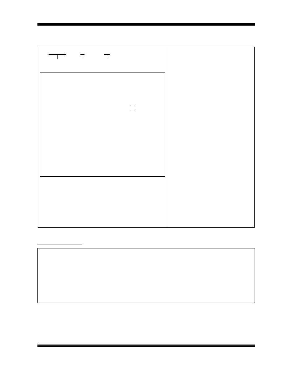
Package Types
V
IN
+
V
IN
≠
MCP6541
V
SS
V
DD
OUT
1
2
3
4
8
7
6
5
-
+
NC
NC
NC
PDIP, SOIC, MSOP
4
1
2
3
-
+
5
SOT-23-5
V
DD
OUT
V
IN
+
V
SS
V
IN
≠
MCP6541-R
MCP6542
V
INA
+
V
INA
≠
V
SS
1
2
3
4
8
7
6
5
-
OUTA
+ -
+
V
DD
OUTB
V
INB
≠
V
INB
+
V
IN
+
V
IN
≠
MCP6543
V
SS
V
DD
OUT
1
2
3
4
8
7
6
5
-
+
NC
CS
NC
PDIP, SOIC, MSOP
PDIP, SOIC, MSOP
MCP6544
V
INA
+
V
INA
≠
V
SS
1
2
3
4
14
13
12
11
-
OUTA
+ -
+
V
DD
OUTD
V
IND
≠
V
IND
+
10
9
8
5
6
7
OUTB
V
INB
≠
V
INB
+
V
INC
+
V
INC
≠
OUTC
+
-
-
+
PDIP, SOIC, TSSOP
4
1
2
3
-
+
5
SOT-23-5, SC-70-5
V
SS
OUT
V
IN
+
V
DD
V
IN
≠
MCP6541
-
+
Push-Pull Output Sub-Microamp Comparators

MCP6541/2/3/4
DS21696C-page 2
2003 Microchip Technology Inc.
1.0
ELECTRICAL
CHARACTERISTICS
1.1
Absolute Maximum Ratings
V
DD
- V
SS
.........................................................................7.0V
All inputs and outputs ...................... V
SS
≠0.3V to V
DD
+0.3V
Difference Input voltage ....................................... |V
DD
- V
SS
|
Output Short-Circuit Current .................................continuous
Current at Input Pins ....................................................±2 mA
Current at Output and Supply Pins ............................±30 mA
Storage temperature .....................................-65∞C to +150∞C
Maximum Junction Temperature (T
J
) ..........................+150∞C
ESD protection on all pins (HBM;MM) ...................4 kV; 400V
Notice: Stresses above those listed under "Maximum Rat-
ings" may cause permanent damage to the device. This is a
stress rating only and functional operation of the device at
those or any other conditions above those indicated in the
operational listings of this specification is not implied.
Exposure to maximum rating conditions for extended periods
may affect device reliability.
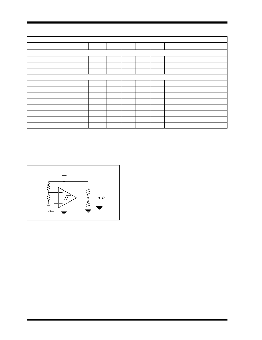
PIN FUNCTION TABLE
DC CHARACTERISTICS
NAME
FUNCTION
V
IN
+, V
INA
+, V
INB
+, V
INC
+,
V
IND
+
Non-Inverting Inputs
V
IN
≠, V
INA
≠, V
INB
≠, V
INC
≠, V
IND
≠ Inverting Inputs
V
DD
Positive Power Supply
V
SS
Negative Power Supply
OUT, OUTA, OUTB, OUTC,
OUTD
Outputs
CS
Chip Select
NC
Not Connected
Electrical Specifications: Unless otherwise indicated, V
DD
= +1.6V to +5.5V, V
SS
= GND, T
A
= +25∞C,V
IN
+ = V
DD
/2,
V
IN≠
= V
SS
, and R
L
= 100 k
to V
DD
/2 (Refer to Figure 1-3).
Parameters
Sym
Min
Typ
Max
Units
Conditions
Power Supply
Supply Voltage
V
DD
1.6
--
5.5
V
Quiescent Current per comparator
I
Q
0.3
0.6
1.0
µA
I
OUT
= 0
Input
Input Voltage Range
V
CMR
V
SS
-0.3
--
V
DD
+0.3
V
Common Mode Rejection Ratio
CMRR
55
70
--
dB
V
DD
= 5V, V
CM
= -0.3V to 5.3V
Common Mode Rejection Ratio
CMRR
50
65
--
dB
V
DD
= 5V, V
CM
= 2.5V to 5.3V
Common Mode Rejection Ratio
CMRR
55
70
--
dB
V
DD
= 5V, V
CM
= -0.3V to 2.5V
Power Supply Rejection Ratio
PSRR
63
80
--
dB
V
CM
= V
SS
Input Offset Voltage
V
OS
-7.0
±1.5
+7.0
mV
V
CM
= V
SS
(Note 1)
Drift with Temperature
V
OS
/
T
A
--
±3
--
µV/∞C T
A
= -40∞C to +85∞C, V
CM
= V
SS
Input Hysteresis Voltage
V
HYST
1.5
3.3
6.5
mV
V
CM
= V
SS
(Note 1)
Drift with Temperature
V
HYST
/
T
A
--
10
--
µV/∞C T
A
= -40∞C to +25∞C, V
CM
= V
SS
Drift with Temperature
V
HYST
/
T
A
--
5
--
µV/∞C T
A
= +25∞C to +85∞C, V
CM
= V
SS
Input Bias Current
I
B
--
1
--
pA
V
CM
=
V
SS
Over-Temperature
I
B
--
--
100
pA
T
A
= -40∞C to +85∞C, V
CM
= V
SS
(Note 3)
Input Offset Current
I
OS
--
±1
--
pA
V
CM
=
V
SS
Common Mode Input Impedance
Z
CM
--
10
13
||4
--
||pF
Differential Input Impedance
Z
DIFF
--
10
13
||2
--
||pF
Push-Pull Output
High-Level Output Voltage
V
OH
V
DD
-0.2
--
--
V
I
OUT
= -2 mA, V
DD
= 5V
Low-Level Output Voltage
V
OL
--
--
V
SS
+0.2
V
I
OUT
= 2 mA, V
DD
= 5V
Short-Circuit Current
I
SC
--
±50
--
mA
(Note 2)
Note 1:
The input offset voltage is the center (average) of the input-referred trip points. The input hysteresis is the difference
between the input-referred trip points.
2:
Limit the output current to Absolute Maximum Rating of 30 mA.
3:
Input bias current over temperature is not tested for SC-70-5 package.

2003 Microchip Technology Inc.
DS21696C-page 3
MCP6541/2/3/4
AC CHARACTERISTICS
SPECIFICATIONS FOR MCP6543 CHIP-SELECT
FIGURE 1-1:
Timing Diagram for the CS
Pin on the MCP6543.
FIGURE 1-2:
Propagation Delay Timing
Diagram.
Electrical Specifications: Unless otherwise indicated, V
DD
= +1.6V to +5.5V, V
SS
= GND, T
A
= +25∞C, V
IN
+ = V
DD
/2,
Step = 200 mV, Overdrive = 100 mV, and C
L
= 36 pF (Refer to Figure 1-2 and Figure 1-3).
Parameters
Sym
Min
Typ
Max
Units
Conditions
Rise Time
t
R
--
0.85
--
µs
Fall Time
t
F
--
0.85
--
µs
Propagation Delay (High-to-Low)
t
PHL
--
4
8
µs
Propagation Delay (Low-to-High)
t
PLH
--
4
8
µs
Propagation Delay Skew
t
PDS
--
±0.2
--
µs
(Note 1)
Maximum Toggle Frequency
f
MAX
--
160
--
kHz
V
DD
= 1.6V
f
MAX
--
120
--
kHz
V
DD
= 5.5V
Input Noise Voltage
E
N
--
200
--
µV
P-P
10 Hz to 100 kHz
Note 1:
Propagation Delay Skew is defined as: t
PDS
= t
PLH
- t
PHL
.
Electrical Specifications: Unless otherwise indicated, V
DD
= +1.6V to +5.5V, V
SS
= GND, T
A
= +25∞C, V
IN
+ = V
DD
/2, V
IN
≠
= V
SS
,
and C
L
= 36 pF (Refer to Figures 1-1 and 1-3).
Parameters
Sym
Min
Typ
Max
Units
Conditions
CS Low Specifications
CS Logic Threshold, Low
V
IL
V
SS
--
0.2V
DD
V
CS Input Current, Low
I
CSL
--
5.0
--
pA
CS = V
SS
CS High Specifications
CS Logic Threshold, High
V
IH
0.8V
DD
--
V
DD
V
CS Input Current, High
I
CSH
--
1
--
pA
CS = V
DD
CS Input High, V
DD
Current
I
DD
--
18
--
pA
CS = V
DD
CS Input High, GND Current
I
SS
--
-20
--
pA
CS = V
DD
Comparator Output Leakage
I
O(LEAK)
--
1
--
pA
V
OUT
= V
DD
CS Dynamic Specifications
CS Low to Comparator Output Low
Turn-on Time
t
ON
--
2
50
ms
CS = 0.2 V
DD
to V
OUT
= V
DD
/2,
V
IN
≠ = V
DD
CS High to Comparator Output
High Z Turn-off Time
t
OFF
--
10
--
µs
CS = 0.8 V
DD
to V
OUT
= V
DD
/2,
V
IN
≠ = V
DD
CS Hysteresis
V
CS_HYST
--
0.6
--
V
V
DD
= 5V
V
IL
Hi-Z
t
ON
V
IH
CS
t
OFF
V
OUT
-20 pA, typ.
Hi-Z
I
SS
I
CS
1 pA, typ.
1 pA, typ.
-20 pA, typ.
-0.6 µA, typ.
V
OL
t
PLH
V
OUT
V
IN
≠
100 mV
100 mV
t
PHL
V
OL
V
IN
+ = V
DD
/2
V
OH
MCP6541/2/3/4
DS21696C-page 4
2003 Microchip Technology Inc.
TEMPERATURE SPECIFICATIONS
1.2
Test Circuit Configuration
This test circuit configuration is used to determine the
AC and DC specifications.
FIGURE 1-3:
AC and DC Test Circuit for
the Push-Pull Output Comparators.
Electrical Specifications: Unless otherwise indicated, V
DD
= +1.6V to +5.5V and V
SS
= GND.
Parameters
Sym
Min
Typ
Max
Units
Conditions
Temperature Ranges
Specified Temperature Range
T
A
-40
--
+85
∞C
Operating Temperature Range
T
A
-40
--
+125
∞C
Note
Storage Temperature Range
T
A
-65
--
+150
∞C
Thermal Package Resistances
Thermal Resistance, 5L-SC-70
JA
--
331
--
∞C/W
Thermal Resistance, 5L-SOT-23
JA
--
256
--
∞C/W
Thermal Resistance, 8L-PDIP
JA
--
85
--
∞C/W
Thermal Resistance, 8L-SOIC
JA
--
163
--
∞C/W
Thermal Resistance, 8L-MSOP
JA
--
206
--
∞C/W
Thermal Resistance, 14L-PDIP
JA
--
70
--
∞C/W
Thermal Resistance, 14L-SOIC
JA
--
120
--
∞C/W
Thermal Resistance, 14L-TSSOP
JA
--
100
--
∞C/W
Note:
The MCP6541/2/3/4 operates over this extended temperature range, but with reduced performance. In any
case, the Junction Temperature (T
J
) must not exceed the Absolute Maximum specification of +150∞C.
V
DD
V
SS
= 0V
200 k
200 k
200 k
200 k
V
OUT
V
IN
= V
SS
36 pF
MCP654X
2003 Microchip Technology Inc.
DS21696C-page 5
MCP6541/2/3/4
2.0
TYPICAL PERFORMANCE CURVES
Note: Unless otherwise indicated, V
DD
= +1.6V to +5.5V, V
SS
= GND, T
A
= +25∞C, V
IN
+ = V
DD
/2, V
IN≠
= GND,
R
L
= 100 k
to V
DD
/2, and C
L
= 36 pF.
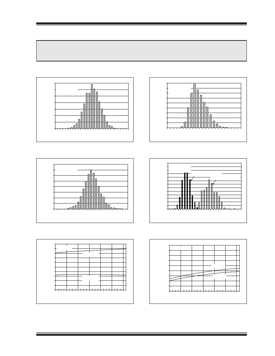
FIGURE 2-1:
Input Offset Voltage
Histogram at V
CM
= V
SS
.
FIGURE 2-2:
Input Offset Voltage Drift
Histogram at V
CM
= V
SS
.
FIGURE 2-3:
Input Offset Voltage vs.
Ambient Temperature at V
CM
= V
SS
.
FIGURE 2-4:
Input Hysteresis Voltage
Histogram at V
CM
= V
SS
.
FIGURE 2-5:
Input Hysteresis Voltage
Drift Histogram.
FIGURE 2-6:
Input Hysteresis Voltage vs.
Ambient Temperature at V
CM
= V
SS
.
Note:
The graphs and tables provided following this note are a statistical summary based on a limited number of
samples and are provided for informational purposes only. The performance characteristics listed herein
are not tested or guaranteed. In some graphs or tables, the data presented may be outside the specified
operating range (e.g., outside specified power supply range) and therefore outside the warranted range.
0%
2%
4%
6%
8%
10%
12%
14%
-7 -6 -5 -4 -3 -2 -1 0 1 2 3 4 5 6 7
Input Offset Voltage (mV)
Percentage of Occurrences
1200 Samples
V
CM
= V
SS
0%
2%
4%
6%
8%
10%
12%
14%
16%
-14 -12 -10 -8 -6 -4 -2 0 2 4 6 8 10 12 14
Input Offset Voltage Drift (µV/∞C)
Percentage of Occurrences
1200 Samples
V
CM
= V
SS
-500
-400
-300
-200
-100
0
100
200
300
400
500
-40
-20
0
20
40
60
80
Ambient Temperature (∞C)
Input Offset Voltage (µV)
V
DD
= 1.6V
V
DD
= 5.5V
V
CM
= V
SS
0%
2%
4%
6%
8%
10%
12%
14%
16%
18%
1.6 2.0 2.4 2.8 3.2 3.6 4.0 4.4 4.8 5.2 5.6 6.0
Input Hysteresis Voltage (mV)
Percentage of Occurrences
1200 Samples
V
CM
= V
SS
0%
2%
4%
6%
8%
10%
12%
14%
16%
18%
20%
22%
24%
26%
2 3 4 5 6 7 8 9 10 11 12 13 14 15 16
Input Hysteresis Voltage Drift (µV/∞C)
Percentage of Occurrences
1200 Samples
V
CM
= V
SS
T
A
= +25∞C to +85∞C
T
A
= -40∞C to +25∞C
1.5
2.0
2.5
3.0
3.5
4.0
4.5
5.0
5.5
6.0
-40
-20
0
20
40
60
80
Ambient Temperature (∞C)
Input Hysteresis Voltage (mV)
V
DD
= 1.6V
V
DD
= 5.5V
V
CM
= V
SS
V
DD
= 1.6V

MCP6541/2/3/4
DS21696C-page 6
2003 Microchip Technology Inc.
Note: Unless otherwise indicated, V
DD
= +1.6V to +5.5V, V
SS
= GND, T
A
= +25∞C, V
IN
+ = V
DD
/2, V
IN≠
= GND,
R
L
= 100 k
to V
DD
/2, and C
L
= 36 pF.
FIGURE 2-7:
Input Offset Voltage vs.
Common Mode Input Voltage at V
DD
= 1.6V.
FIGURE 2-8:
Input Offset Voltage vs.
Common Mode Input Voltage at V
DD
= 5.5V.
FIGURE 2-9:
CMRR, PSRR vs. Ambient
Temperature at V
CM
= V
SS
.
FIGURE 2-10:
Input Hysteresis Voltage vs.
Common Mode Input Voltage at V
DD
= 1.6V.
FIGURE 2-11:
Input Hysteresis Voltage vs.
Common Mode Input Voltage at V
DD
= 5.5V.
FIGURE 2-12:
Input Bias Current, Input
Offset Current vs. Common Mode Voltage at
+85∞C.
-2.0
-1.5
-1.0
-0.5
0.0
0.5
1.0
1.5
2.0
-0.4
-0.2
0.0
0.2
0.4
0.6
0.8
1.0
1.2
1.4
1.6
1.8
2.0
Common Mode Input Voltage (V)
Input Offset Voltage (mV)
T
A
= +85∞C
T
A
= +25∞C
T
A
= -40∞C
V
DD
= 1.6V
-2.0
-1.5
-1.0
-0.5
0.0
0.5
1.0
1.5
2.0
-0.5
0.0
0.5
1.0
1.5
2.0
2.5
3.0
3.5
4.0
4.5
5.0
5.5
6.0
Common Mode Input Voltage (V)
Input Offset Voltage (mV)
T
A
= -40∞C
T
A
= +25∞C
T
A
= +85∞C
V
DD
= 5.5V
55
60
65
70
75
80
85
90
-40
-20
0
20
40
60
80
Ambient Temperature (∞C)
CMRR, PSRR; Input Referred
(dB)
CMRR, V
IN
+ = 2.5V to 5.3V, V
DD
= 5.0V
CMRR, V
IN
+ = -0.3V to 2.5V, V
DD
= 5.0V
CMRR, V
IN
+ = -0.3V to 5.3V, V
DD
= 5.0V
PSRR, V
IN
+ = V
SS
, V
DD
= 1.6V to 5.5V
1.5
2.0
2.5
3.0
3.5
4.0
4.5
5.0
5.5
6.0
-0.4
-0.2
0.0
0.2
0.4
0.6
0.8
1.0
1.2
1.4
1.6
1.8
2.0
Common Mode Input Voltage (V)
Input Hysteresis Voltage (mV)
T
A
= -40∞C
T
A
= +85∞C
T
A
= +25∞C
V
DD
= 1.6V
1.5
2.0
2.5
3.0
3.5
4.0
4.5
5.0
5.5
6.0
-0.5
0.0
0.5
1.0
1.5
2.0
2.5
3.0
3.5
4.0
4.5
5.0
5.5
6.0
Common Mode Input Voltage (V)
Input Hysteresis Voltage (mV)
V
DD
= 5.5V
T
A
= +25∞C
T
A
= -40∞C
T
A
= +85∞C
0
2
4
6
8
10
12
14
16
18
20
22
24
0.0 0.5 1.0 1.5 2.0 2.5 3.0 3.5 4.0 4.5 5.0 5.5
Common Mode Input Voltage (V)
Input Current (pA)
Input Bias Current
Input Offset Current
T
A
= +85∞C
V
DD
= 5.5V

2003 Microchip Technology Inc.
DS21696C-page 7
MCP6541/2/3/4
Note: Unless otherwise indicated, V
DD
= +1.6V to +5.5V, V
SS
= GND, T
A
= +25∞C, V
IN
+ = V
DD
/2, V
IN≠
= GND,
R
L
= 100 k
to V
DD
/2, and C
L
= 36 pF.
FIGURE 2-13:
Input Bias Current, Input
Offset Current vs. Ambient Temperature.
FIGURE 2-14:
Quiescent Current vs.
Ambient Temperature.
FIGURE 2-15:
Quiescent Current vs.
Common Mode Input Voltage at V
DD
= 1.6V.
FIGURE 2-16:
Quiescent Current vs.
Power Supply Voltage.
FIGURE 2-17:
Quiescent Current vs.
Common Mode Input Voltage at V
DD
= 5V.
FIGURE 2-18:
Output Short-Circuit Current
vs. Power Supply Voltage.
-2
0
2
4
6
8
10
12
14
16
18
20
22
25
35
45
55
65
75
85
Ambient Temperature (∞C)
Input Current (pA)
Input Bias Current
Input Offset
Current
V
DD
= 5.5V
V
CM
= V
DD
0.0
0.1
0.2
0.3
0.4
0.5
0.6
0.7
-40
-20
0
20
40
60
80
Ambient Temperature (∞C)
Quiescent Current
(µA/comparator)
V
DD
= 5.5 V
V
DD
= 1.6 V
0.0
0.1
0.2
0.3
0.4
0.5
0.6
0.7
-0.4
-0.2
0.0
0.2
0.4
0.6
0.8
1.0
1.2
1.4
1.6
1.8
2.0
Common Mode Input Voltage (V)
Quiescent Current
(µA/comparator)
V
DD
= 1.6V
Sweep V
IN+
, V
IN-
= V
DD
/2 Sweep V
IN-
, V
IN+
= V
DD
/2
0.0
0.1
0.2
0.3
0.4
0.5
0.6
0.7
0.0 0.5 1.0 1.5 2.0 2.5 3.0 3.5 4.0 4.5 5.0 5.5
Power Supply Voltage (V)
Quiescent Current
(µA/comparator)
T
A
= -40∞C
T
A
= +85∞C
T
A
= +25∞C
0.0
0.1
0.2
0.3
0.4
0.5
0.6
0.7
-0.5
0.0
0.5
1.0
1.5
2.0
2.5
3.0
3.5
4.0
4.5
5.0
5.5
6.0
Common Mode Input Voltage (V)
Quiescent Current
(µA/comparator)
V
DD
= 5.5V
Sweep V
IN
+, V
IN
≠ = V
DD
/2
Sweep V
IN
≠, V
IN
+ = V
DD
/2
0
5
10
15
20
25
30
35
40
45
50
1.5
2.0
2.5
3.0
3.5
4.0
4.5
5.0
5.5
Power Supply Voltage (V)
Output Short Circuit Current
(mA)
-I
OSC
, T
A
= -40∞C
-I
OSC
, T
A
= +25∞C
-I
OSC
, T
A
= +85∞C
|+I
OSC
|, T
A
= -40∞C
|+I
OSC
|, T
A
= +85∞C
|+I
OSC
|, T
A
= +25∞C
MCP6541/2/3/4
DS21696C-page 8
2003 Microchip Technology Inc.
Note: Unless otherwise indicated, V
DD
= +1.6V to +5.5V, V
SS
= GND, T
A
= +25∞C, V
IN
+ = V
DD
/2, V
IN≠
= GND,
R
L
= 100 k
to V
DD
/2, and C
L
= 36 pF.
FIGURE 2-19:
Output Voltage Headroom
vs. Output Current at V
DD
= 1.6V.
FIGURE 2-20:
High-to-Low Propagation
Delay Histogram.
FIGURE 2-21:
Propagation Delay Skew
Histogram.
FIGURE 2-22:
Output Voltage Headroom
vs. Output Current at V
DD
= 5.5V.
FIGURE 2-23:
Low-to-High Propagation
Delay Histogram.
FIGURE 2-24:
Propagation Delay vs.
Ambient Temperature.
0.0
0.1
0.2
0.3
0.4
0.5
0.6
0.7
0.8
0.9
1.0
0.0
0.5
1.0
1.5
2.0
2.5
Output Current (mA)
Output Voltage Headroom (V)
V
DD
= 1.6V
V
OL
-V
SS
, T
A
= -40∞C
V
OL
-V
SS
, T
A
= +25∞C
V
OL
-V
SS
, T
A
= +85∞C
V
DD
-V
OH
, T
A
= +85∞C
V
DD
-V
OH
, T
A
= +25∞C
V
DD
-V
OH
, T
A
= -40∞C
0%
5%
10%
15%
20%
25%
30%
35%
40%
45%
0
1
2
3
4
5
6
7
8
High-to-Low Propagation Delay (µs)
Percentage of Occurrences
600 Samples
100 mV Overdrive
V
CM
= V
DD
/2
V
DD
= 5.5V
V
DD
= 1.6V
0%
5%
10%
15%
20%
25%
30%
35%
40%
45%
-2.0 -1.5 -1.0 -0.5
0.0
0.5
1.0
1.5
2.0
Propagation Delay Skew (µs)
Percentage of Occurrences
600 Samples
100 mV Overdrive
V
CM
= V
DD
/2
V
DD
= 1.6V
V
DD
= 5.5V
0.0
0.1
0.2
0.3
0.4
0.5
0.6
0.7
0.8
0.9
1.0
0
5
10
15
20
25
Output Current (mA)
Output Voltage Headroom (V)
V
DD
= 5.5V
V
OL
-V
SS
, T
A
= -40∞C
V
OL
-V
SS
, T
A
= +25∞C
V
OL
-V
SS
, T
A
= +85∞C
V
DD
-V
OH
, T
A
= +85∞C
V
DD
-V
OH
, T
A
= +25∞C
V
DD
-V
OH
, T
A
= -40∞C
0%
5%
10%
15%
20%
25%
30%
35%
40%
45%
0
1
2
3
4
5
6
7
8
Low-to-High Propagation Delay (µs)
Percentage of Occurrences
600 Samples
100 mV Overdrive
V
CM
= V
DD
/2
V
DD
= 5.5V
V
DD
= 1.6V
0
1
2
3
4
5
6
7
8
-40
-20
0
20
40
60
80
Ambient Temperature (∞C)
Propagation Delay (µs)
100 mV Overdrive
V
CM
= V
DD
/2
t
PLH
@ V
DD
= 1.6V
t
PHL
@ V
DD
= 1.6V
t
PLH
@ V
DD
= 5.5V
t
PHL
@ V
DD
= 5.5V
2003 Microchip Technology Inc.
DS21696C-page 9
MCP6541/2/3/4
Note: Unless otherwise indicated, V
DD
= +1.6V to +5.5V, V
SS
= GND, T
A
= +25∞C, V
IN
+ = V
DD
/2, V
IN≠
= GND,
R
L
= 100 k
to V
DD
/2, and C
L
= 36 pF.
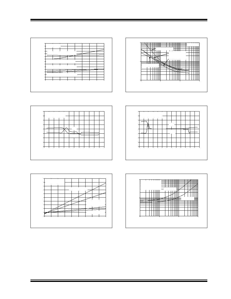
FIGURE 2-25:
Propagation Delay vs.
Power Supply Voltage.
FIGURE 2-26:
Propagation Delay vs.
Common Mode Input Voltage at V
DD
= 1.6V.
FIGURE 2-27:
Propagation Delay vs. Load
Capacitance.
FIGURE 2-28:
Propagation Delay vs. Input
Overdrive.
FIGURE 2-29:
Propagation Delay vs.
Common Mode Input Voltage at V
DD
= 5.5V.
FIGURE 2-30:
Supply Current vs. Toggle
Frequency.
0
1
2
3
4
5
6
7
8
9
10
11
12
13
14
1.5
2.0
2.5
3.0
3.5
4.0
4.5
5.0
5.5
Power Supply Voltage (V)
Propagation Delay (µs)
V
CM
= V
DD
/2
t
PLH
@ 100 mV Overdrive
t
PHL
@ 100 mV Overdrive
t
PLH
@ 10 mV Overdrive
t
PHL
@ 10 mV Overdrive
0
1
2
3
4
5
6
7
8
-0.4
-0.2
0.0
0.2
0.4
0.6
0.8
1.0
1.2
1.4
1.6
1.8
2.0
Common Mode Input Voltage (V)
Propagation Delay (µs)
V
DD
= 1.6V
100 mV Overdrive
t
PLH
t
PHL
0
5
10
15
20
25
30
35
40
45
50
0
10
20
30
40
50
60
70
80
90
Load Capacitance (nF)
Propagation Delay (µs)
100 mV Overdrive
V
CM
= V
DD
/2
t
PHL
@ V
DD
= 1.6V
t
PLH
@ V
DD
= 1.6V
t
PHL
@ V
DD
= 5.5V
t
PLH
@ V
DD
= 5.5V
1
10
100
1
10
100
1000
Input Overdrive (mV)
Propagation Delay (µs)
V
CM
= V
DD
/2
t
PLH
@ V
DD
= 1.6V
t
PHL
@ V
DD
= 1.6V
t
PLH
@ V
DD
= 5.5V
t
PHL
@ V
DD
= 5.5V
0
1
2
3
4
5
6
7
8
-0.5
0.0
0.5
1.0
1.5
2.0
2.5
3.0
3.5
4.0
4.5
5.0
5.5
6.0
Common Mode Input Voltage (V)
Propagation Delay (µs)
V
DD
= 5.5V
100 mV Overdrive
t
PHL
t
PLH
0.1
1
10
0.1
1
10
100
Toggle Frequency (kHz)
Supply Current (µA)
V
DD
= 5.5 V
V
DD
= 1.6 V
100 mV Overdrive
V
CM
= V
DD
/2
R
L
= Infinity

MCP6541/2/3/4
DS21696C-page 10
2003 Microchip Technology Inc.
Note: Unless otherwise indicated, V
DD
= +1.6V to +5.5V, V
SS
= GND, T
A
= +25∞C, V
IN
+ = V
DD
/2, V
IN≠
= GND,
R
L
= 100 k
to V
DD
/2, and C
L
= 36 pF.
FIGURE 2-31:
The MCP6541/2/3/4
comparators show no phase reversal.
FIGURE 2-32:
Supply Current (shoot
through current) vs. Chip-Select (CS) Voltage at
V
DD
= 1.6V (MCP6543 only).
FIGURE 2-33:
Supply Current (charging
current) vs. Chip-Select (CS) pulse at
V
DD
= 1.6V (MCP6543 only).
FIGURE 2-34:
Chip-Select (CS) Step
Response (MCP6543 only).
FIGURE 2-35:
Supply Current (shoot
through current) vs. Chip-Select (CS) Voltage at
V
DD
= 5.5V (MCP6543 only).
FIGURE 2-36:
Supply Current (charging
current) vs. Chip-Select (CS) pulse at
V
DD
= 5.5V (MCP6543 only).
-1
0
1
2
3
4
5
6
7
0
1
2
3
4
5
6
7
8
9
10
Time (1 ms/div)
Inverting Input, Output Voltage (V)
V
OUT
V
IN
≠
V
DD
= 5.5V
1.E-11
1.E-10
1.E-09
1.E-08
1.E-07
1.E-06
1.E-05
1.E-04
0.0
0.2
0.4
0.6
0.8
1.0
1.2
1.4
1.6
Chip Select (CS) Voltage (V)
Supply Current (A/comparator)
Comparator
Shuts Off Here
Comparator
Turns On Here
100µ
10p
100p
1n
10n
100n
1µ
V
DD
= 1.6V
CS Hysteresis
CS High-to-Low
CS Low-to-High
10µ
0
5
10
15
20
25
30
0
1
2
3
4
5
6
7
8
9
10
11
12
13
14
Time (1 ms/div)
Supply Current
(µA/Comparator)
-8.1
-6.5
-4.9
-3.2
-1.6
0.0
1.6
Output Voltage,
Chip Select Voltage (V),
Start-up I
DD
Charging output
capacitance
V
DD
= 1.6V
V
OUT
CS
-0.5
0.0
0.5
1.0
1.5
2.0
2.5
3.0
3.5
4.0
4.5
5.0
5.5
6.0
0
1
2
3
4
5
6
7
8
9
10
Time (ms)
Chip Select, Output Voltage (V)
V
OUT
CS
V
DD
= 5.5V
1.E-11
1.E-10
1.E-09
1.E-08
1.E-07
1.E-06
1.E-05
1.E-04
0.0
0.5
1.0
1.5
2.0
2.5
3.0
3.5
4.0
4.5
5.0
5.5
Chip Select (CS) Voltage (V)
Supply Current (A/Comparator)
Comparator
Shuts Off Here
Comparator
Turns On Here
V
DD
= 5.5V
100µ
1µ
10µ
100n
1n
10n
100p
10p
CS High-to-Low
CS Low-to-High
CS Hysteresis
0
20
40
60
80
100
120
140
160
180
200
0.0
0.5
1.0
1.5
2.0
2.5
3.0
3.5
Time (0.5 ms/div)
Supply Current
(µA/Comparator)
-24
-21
-18
-15
-12
-9
-6
-3
0
3
6
Output Voltage,
Chip Select Voltage (V)
Start-up I
DD
Charging output
capacitance
V
DD
= 5.5V
V
OUT
CS
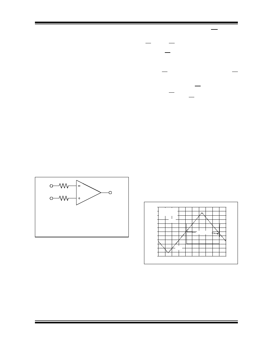
2003 Microchip Technology Inc.
DS21696C-page 11
MCP6541/2/3/4
3.0
APPLICATIONS INFORMATION
The MCP6541/2/3/4 family of push-pull output compar-
ators are fabricated on Microchip's state-of-the-art
CMOS process. They are suitable for a wide range of
applications requiring very low power consumption.
3.1
Comparator Inputs
The MCP6541/2/3/4 comparator family uses CMOS
transistors at the input. They are designed to prevent
phase inversion when the input pins exceed the supply
voltages. Figure 2-31 shows an input voltage
exceeding both supplies with no resulting phase
inversion.
The input stage of this family of devices uses two
differential input stages in parallel: one operates at low
input voltages and the other at high input voltages. With
this topology, the input voltage is 0.3V above V
DD
and
0.3V below V
SS
. Therefore, the input offset voltage is
measured at both V
SS
- 0.3V and V
DD
+ 0.3V to ensure
proper operation.
The maximum operating input voltages that can be
applied are V
SS
- 0.3V and V
DD
+ 0.3V. Voltages on the
inputs that exceed this absolute maximum rating can
cause excessive current to flow and permanently
damage the device. In applications where the input pin
exceeds the specified range, external resistors can be
used to limit the current below ±2 mA, as shown in
Figure 3-1.
FIGURE 3-1:
An input resistor (R
IN
)
should be used to limit excessive input current if
either of the inputs exceeds the Absolute
Maximum specification.
3.2
Push-Pull Output
The push-pull output is designed to be compatible with
CMOS and TTL logic, while the output transistors are
configured to give rail-to-rail output performance. They
are driven with circuitry that minimizes any switching
current (shoot-through current from supply-to-supply)
when the output is transitioned from high-to-low, or from
low-to-high (see Figures 2-15, 2-17, 2-32 through 2-36
for more information).
3.3
MCP6543 Chip Select (CS)
The MCP6543 is a single comparator with chip select
(CS). When CS is pulled high, the total current
consumption drops to 20 pA (typ); 1 pA (typ) flows
through the CS pin, 1 pA (typ) flows through the output
pin and 18 pA (typ) flows through the V
DD
pin, as
shown in Figure 1-1. When this happens, the
comparator output is put into a high-impedance state.
By pulling CS low, the comparator is enabled. If the CS
pin is left floating, the comparator will not operate
properly. Figure 1-1 shows the output voltage and
supply current response to a CS pulse.
The internal CS circuitry is designed to minimize
glitches when cycling the CS pin. This helps conserve
power, which is especially important in battery-
powered applications.
3.4
Externally-Set Hysteresis
Greater flexibility in selecting hysteresis (or input trip
points) is achieved by using external resistors.
Input offset voltage (V
OS
) is the center (average) of the
(input-referred) low-high and high-low trip points. Input
hysteresis voltage (V
HYST
) is the difference between
the same trip points. Hysteresis reduces output
chattering when one input is slowly moving past the
other and thus reduces dynamic supply current. It also
helps in systems where it is best not to cycle between
states too frequently (e.g., air conditioner thermostatic
control). The MCP6541/2/3/4 family has internally-set
hysteresis that is small enough to maintain input offset
accuracy (<7 mV) and large enough to eliminate output
chattering caused by the comparator's own input noise
voltage (200 µVp-p).
FIGURE 3-2:
The MCP6541/2/3/4
comparators' internal hysteresis eliminates
output chatter caused by input noise voltage.
RIN
VSS Minimum expected VIN
(
)
≠
2 mA
------------------------------------------------------------------------------
RIN
Maximum expected VIN
(
) VDD
≠
2 mA
----------------------------------------------------------------------------------
V
IN
R
IN
V
OUT
MCP654X
-3
-2
-1
0
1
2
3
4
5
6
7
8
9
0
100
200
300
400
500
600
700
800
900
1000
Time (100 ms/div)
Output Voltage (V)
-30
-25
-20
-15
-10
-5
0
5
10
15
20
25
30
Input Voltage (10 mV/div)
V
OUT
V
IN
≠
Hysteresis
V
DD
= 5.0V
V
IN
+ = +2.75V

MCP6541/2/3/4
DS21696C-page 12
2003 Microchip Technology Inc.
3.4.1
NON-INVERTING CIRCUIT
Figure 3-3 shows a non-inverting circuit for single-
supply applications using just two resistors. The
resulting hysteresis diagram is shown in Figure 3-4.
FIGURE 3-3:
Non-inverting circuit with
hysteresis for single-supply.
FIGURE 3-4:
Hysteresis Diagram for the
Non-Inverting Circuit.
The trip points for Figures 3-3 and 3-4 are:
EQUATION
3.4.2
INVERTING CIRCUIT
Figure 3-5 shows an inverting circuit for single-supply
using three resistors. The resulting hysteresis diagram
is shown in Figure 3-6.
FIGURE 3-5:
Inverting Circuit With
Hysteresis.
FIGURE 3-6:
Hysteresis Diagram for the
Inverting Circuit.
In order to determine the trip voltages (V
THL
and V
TLH
)
for the circuit shown in Figure 3-5, R
2
and R
3
can be
simplified to the Thevenin equivalent circuit with
respect to V
DD
, as shown in Figure 3-7.
FIGURE 3-7:
Thevenin Equivalent Circuit.
V
REF
V
IN
V
OUT
MCP654X
V
DD
R
1
R
F
+
-
V
OUT
High-to-Low
Low-to-High
V
DD
V
OH
V
OL
V
SS
V
SS
V
DD
V
THL
V
TLH
V
IN
VTLH
VREF 1
R1
RF
-------
+
VOL
R1
RF
-------
≠
=
VTHL
VREF 1
R1
RF
-------
+
VOH
R1
RF
-------
≠
=
V
TLH
= trip voltage from low to high
V
THL
= trip voltage from high to low
V
IN
V
OUT
MCP654X
V
DD
R
2
R
F
R
3
V
DD
V
OUT
High-to-Low
Low-to-High
V
DD
V
OH
V
OL
V
SS
V
SS
V
DD
V
TLH
V
THL
V
IN
V
23
V
OUT
MCP654X
V
DD
R
23
R
F
+
-
V
SS
2003 Microchip Technology Inc.
DS21696C-page 13
MCP6541/2/3/4
Where:
Using this simplified circuit, the trip voltage can be
calculated using the following equation:
EQUATION
Figure 2-19 and Figure 2-22 can be used to determine
typical values for V
OH
and V
OL
.
3.5
Bypass Capacitors
With this family of comparators, the power supply pin
(V
DD
for single supply) should have a local bypass
capacitor (i.e., 0.01 µF to 0.1 µF) within 2 mm for good
edge rate performance.
3.6
Capacitive Loads
Reasonable capacitive loads (e.g., logic gates) have
little impact on propagation delay (see Figure 2-27).
The supply current increases with increasing toggle
frequency (Figure 2-30), especially with higher
capacitive loads.
3.7
Battery Life
In order to maximize battery life in portable
applications, use large resistors and small capacitive
loads. Also, avoid toggling the output more than
necessary and do not use chip select (CS) to conserve
power for short periods of time. Capacitive loads will
draw additional power at start-up.
3.8
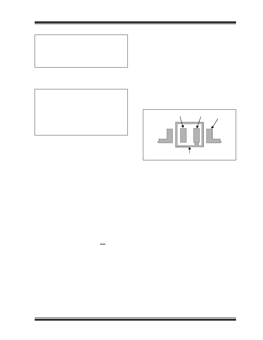
PCB Surface Leakage
In applications where low input bias current is critical,
PCB (Printed Circuit Board) surface leakage effects
need to be considered. Surface leakage is caused by
humidity, dust or other contamination on the board.
Under low humidity conditions, a typical resistance
between nearby traces is 10
12
. A 5V difference would
cause 5 pA, if current-to-flow. This is greater than the
MCP6541/2/3/4 family's bias current at 25∞C (1 pA,
typ).
The easiest way to reduce surface leakage is to use a
guard ring around sensitive pins (or traces). The guard
ring is biased at the same voltage as the sensitive pin.
An example of this type of layout is shown in
Figure 3-8.
FIGURE 3-8:
Example Guard Ring Layout
for Inverting Circuit.
1.
Inverting Configuration (Figures 3-5 and 3-8):
a.
Connect the guard ring to the non-inverting
input pin (V
IN
+). This biases the guard ring
to the same reference voltage as the
comparator (e.g., V
DD
/2 or ground).
b.
Connect the inverting pin (V
IN
≠) to the input
pad without touching the guard ring.
2.
Non-inverting Configuration (Figure 3-3):
a.
Connect the non-inverting pin (V
IN
+) to the
input pad without touching the guard ring.
b.
Connect the guard ring to the inverting input
pin (V
IN
≠).
R
23
R
2
R
3
R
2
R
3
+
------------------
=
V
23
R
3
R
2
R
3
+
------------------ V
DD
◊
=
V
THL
V
OH
R
23
R
23
RF
+
-----------------------
V
23
R
F
R
23
R
F
+
----------------------
+
=
V
TLH
V
OL
R
23
R
23
RF
+
-----------------------
V
23
R
F
R
23
R
F
+
----------------------
+
=
V
TLH
= trip voltage from low to high
V
THL
= trip voltage from high to low
Guard Ring
V
SS
V
IN
-
V
IN
+

MCP6541/2/3/4
DS21696C-page 14
2003 Microchip Technology Inc.
3.9
Typical Applications
3.9.1
PRECISE COMPARATOR
Some applications require higher DC precision. An
easy way to solve this problem is to use an amplifier
(such as the MCP6041) to gain-up the input signal
before it reaches the comparator. Figure 3-9 shows an
example of this approach.
FIGURE 3-9:
Precise Inverting
Comparator.
3.9.2
WINDOWED COMPARATOR
Figure 3-10 shows one approach to designing a win-
dowed comparator. The AND gate produces a logic `1'
when the input voltage is between V
RB
and V
RT
(where
V
RT
> V
RB
).
FIGURE 3-10:
Windowed Comparator.
3.9.3
BISTABLE MULTI-VIBRATOR
A simple bistable multi-vibrator design is shown in
Figure 3-11. V
REF
needs to be between the power
supplies (V
SS
= GND and V
DD
) to achieve oscillation.
The output duty cycle changes with V
REF
.
FIGURE 3-11:
Bistable Multi-vibrator.
V
REF
V
DD
V
DD
R
1
R
2
V
OUT
V
IN
V
REF
MCP6041
MCP654X
V
RT
MCP6542
V
RB
V
IN
1/2
MCP6542
1/2
MCP6541
V
DD
R
1
R
2
R
3
V
REF
C
1
V
OUT

2003 Microchip Technology Inc.
DS21696C-page 15
MCP6541/2/3/4
4.0
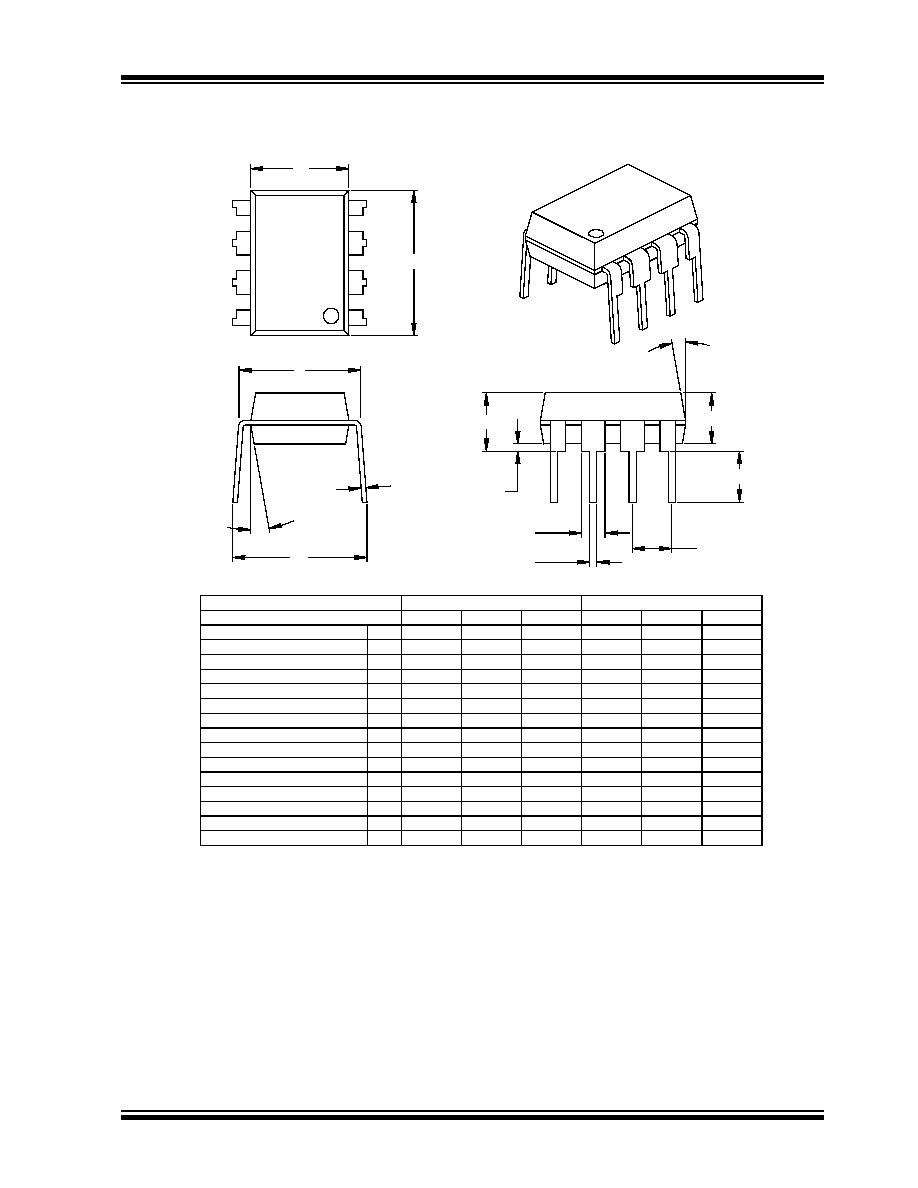
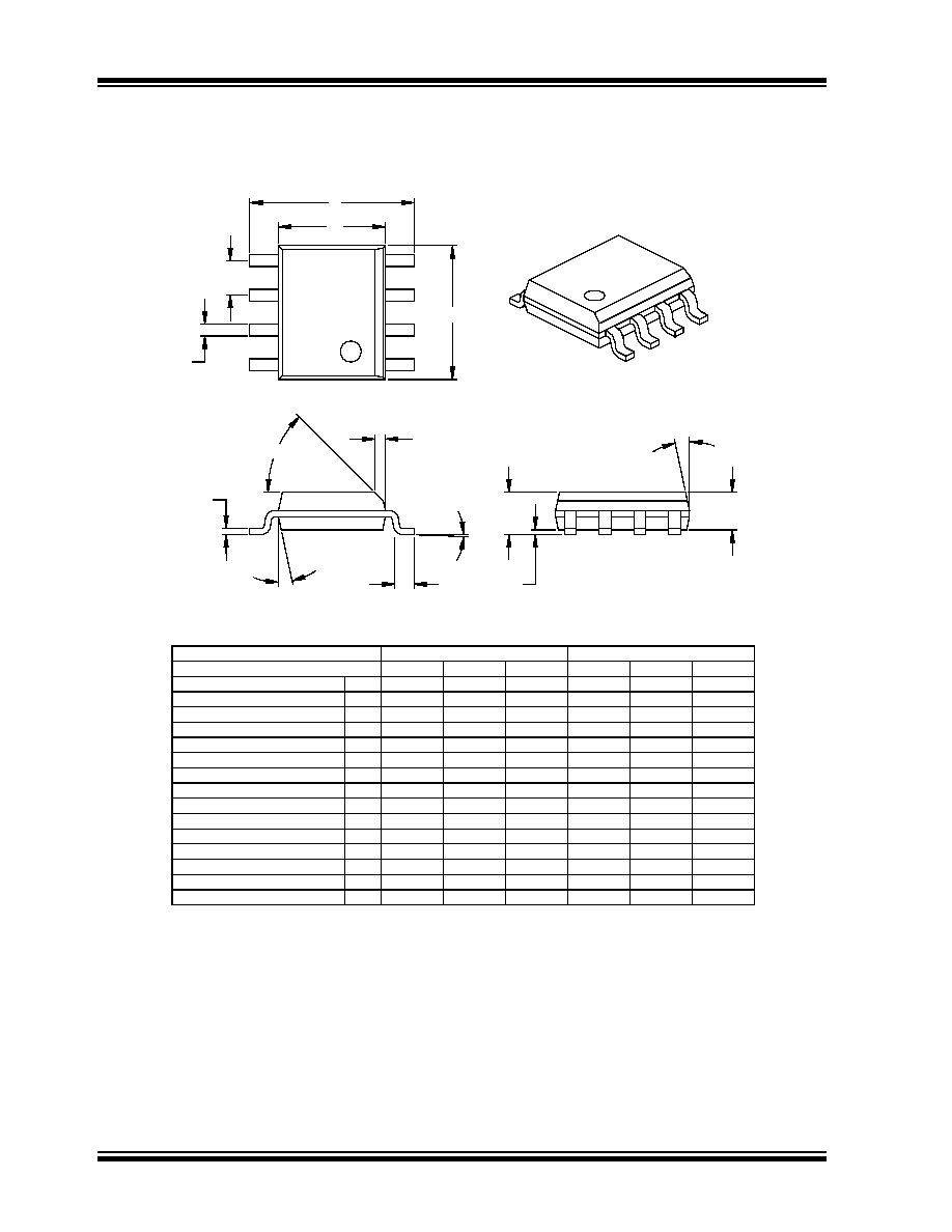
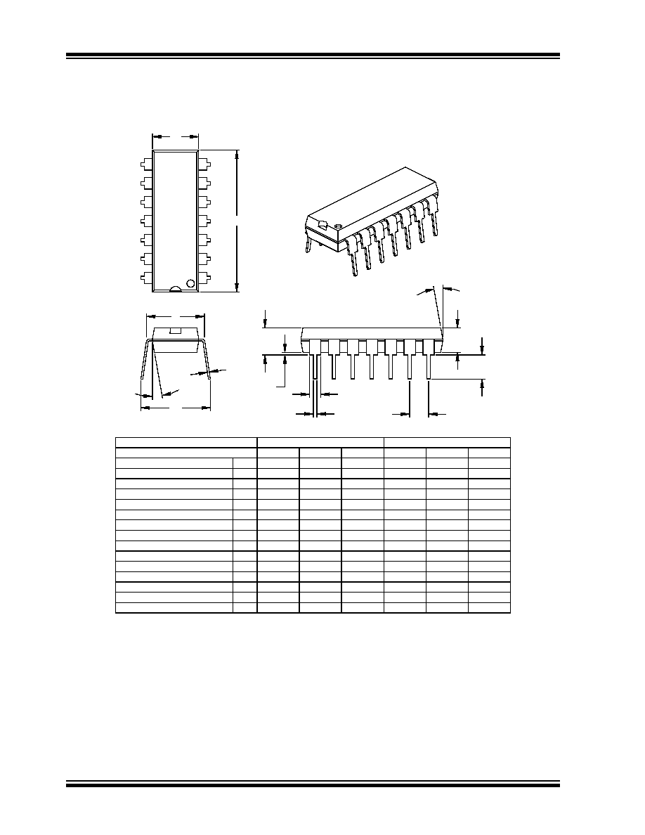
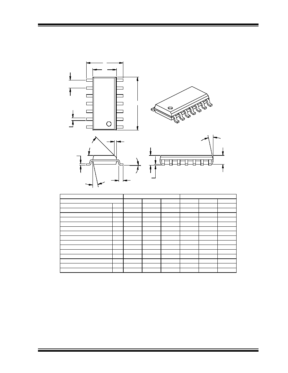
PACKAGING INFORMATION
4.1
Package Marking Information
XXXXXXXX
XXXXXNNN
YYWW
8-Lead PDIP (300 mil)
Example
:
8-Lead SOIC (150 mil)
Example
:
XXXXXXXX
XXXXYYWW
NNN
Legend: XX...X Customer specific information*
YY
Year code (last 2 digits of calendar year)
WW
Week code (week of January 1 is week `01')
NNN
Alphanumeric traceability code
Note:
In the event the full Microchip part number cannot be marked on one line, it will
be carried over to the next line thus limiting the number of available characters
for customer specific information.
*
Standard marking consists of Microchip part number, year code, week code, traceability code (facility
code, mask rev#, and assembly code). For marking beyond this, certain price adders apply. Please
check with your Microchip Sales Office.
MCP6541
I/P256
0307
MCP6542
I/SN0307
256
8-Lead MSOP
Example
:
XXXXXX
YWWNNN
6543I
307256
5-Lead SOT-23 (MCP6541)
Example:
XXNN
AB37
5-Lead SC-70 (MCP6541)
Example:
XNN
YWW
A25
307
MCP6541/2/3/4
DS21696C-page 16
2003 Microchip Technology Inc.
Package Marking Information (Continued)
14-Lead PDIP (300 mil) (MCP6544)
Example
:
14-Lead TSSOP (MCP6544)
Example
:
14-Lead SOIC (150 mil) (MCP6544)
Example:
XXXXXXXXXXXXXX
XXXXXXXXXXXXXX
YYWWNNN
XXXXXXXXXX
YYWWNNN
XXXXXXXX
YYWW
NNN
MCP6544
-I/P
0307256
MCP6544I
0307
256
XXXXXXXXXX
MCP6544ISL
0307256

2003 Microchip Technology Inc.
DS21696C-page 17
MCP6541/2/3/4
5-Lead Plastic Package (LT) (SC-70)
0.30
0.15
.012
.006
B
Lead Width
0.18
0.10
.007
.004
c
Lead Thickness
0.30
0.10
.012
.004
L
Foot Length
2.20
1.80
.087
.071
D
Overall Length
1.35
1.15
.053
.045
E1
Molded Package Width
2.40
1.80
.094
.071
E
Overall Width
0.10
0.00
.004
.000
A1
Standoff
1.00
0.80
.039
.031
A2
Molded Package Thickness
1.10
0.80
.043
.031
A
Overall Height
0.65 (BSC)
.026 (BSC)
p
Pitch
5
5
n
Number of Pins
MAX
NOM
MIN
MAX
NOM
MIN
Dimension Limits
MILLIMETERS*
INCHES
Units
exceed .005" (0.127mm) per side.
Dimensions D and E1 do not include mold flash or protrusions. Mold flash or protrusions shall not
Notes:
JEITA (EIAJ) Standard: SC-70
Drawing No. C04-061
*Controlling Parameter
L
E1
E
c
D
1
B
p
A2
A1
A
Q1
Top of Molded Pkg to Lead Shoulder
Q1
.004
.016
0.10
0.40
n
MCP6541/2/3/4
DS21696C-page 18
2003 Microchip Technology Inc.
5-Lead Plastic Small Outline Transistor (OT) (SOT23)
10
5
0
10
5
0
Mold Draft Angle Bottom
10
5
0
10
5
0
Mold Draft Angle Top
0.50
0.43
0.35
.020
.017
.014
B
Lead Width
0.20
0.15
0.09
.008
.006
.004
c
Lead Thickness
10
5
0
10
5
0
Foot Angle
0.55
0.45
0.35
.022
.018
.014
L
Foot Length
3.10
2.95
2.80
.122
.116
.110
D
Overall Length
1.75
1.63
1.50
.069
.064
.059
E1
Molded Package Width
3.00
2.80
2.60
.118
.110
.102
E
Overall Width
0.15
0.08
0.00
.006
.003
.000
A1
Standoff ß
1.30
1.10
0.90
.051
.043
.035
A2
Molded Package Thickness
1.45
1.18
0.90
.057
.046
.035
A
Overall Height
1.90
.075
p1
Outside lead pitch (basic)
0.95
.038
p
Pitch
5
5
n
Number of Pins
MAX
NOM
MIN
MAX
NOM
MIN
Dimension Limits
MILLIMETERS
INCHES*
Units
1
p
D
B
n
E
E1
L
c
A2
A
A1
p1
* Controlling Parameter
Notes:
Dimensions D and E1 do not include mold flash or protrusions. Mold flash or protrusions shall not exceed
.010" (0.254mm) per side.
JEDEC Equivalent: MO-178
Drawing No. C04-091
ß Significant Characteristic
2003 Microchip Technology Inc.
DS21696C-page 19
MCP6541/2/3/4
8-Lead Plastic Dual In-line (P) ≠ 300 mil (PDIP)
B1
B
A1
A
L
A2
p
E
eB
c
E1
n
D
1
2
Units
INCHES*
MILLIMETERS
Dimension Limits
MIN
NOM
MAX
MIN
NOM
MAX
Number of Pins
n
8
8
Pitch
p
.100
2.54
Top to Seating Plane
A
.140
.155
.170
3.56
3.94
4.32
Molded Package Thickness
A2
.115
.130
.145
2.92
3.30
3.68
Base to Seating Plane
A1
.015
0.38
Shoulder to Shoulder Width
E
.300
.313
.325
7.62
7.94
8.26
Molded Package Width
E1
.240
.250
.260
6.10
6.35
6.60
Overall Length
D
.360
.373
.385
9.14
9.46
9.78
Tip to Seating Plane
L
.125
.130
.135
3.18
3.30
3.43
Lead Thickness
c
.008
.012
.015
0.20
0.29
0.38
Upper Lead Width
B1
.045
.058
.070
1.14
1.46
1.78
Lower Lead Width
B
.014
.018
.022
0.36
0.46
0.56
Overall Row Spacing
ß
eB
.310
.370
.430
7.87
9.40
10.92
Mold Draft Angle Top
5
10
15
5
10
15
Mold Draft Angle Bottom
5
10
15
5
10
15
* Controlling Parameter
Notes:
Dimensions D and E1 do not include mold flash or protrusions. Mold flash or protrusions shall not exceed
JEDEC Equivalent: MS-001
Drawing No. C04-018
.010" (0.254mm) per side.
ß Significant Characteristic
MCP6541/2/3/4
DS21696C-page 20
2003 Microchip Technology Inc.
8-Lead Plastic Small Outline (SN) ≠ Narrow, 150 mil (SOIC)
Foot Angle
0
4
8
0
4
8
15
12
0
15
12
0
Mold Draft Angle Bottom
15
12
0
15
12
0
Mold Draft Angle Top
0.51
0.42
0.33
.020
.017
.013
B
Lead Width
0.25
0.23
0.20
.010
.009
.008
c
Lead Thickness
0.76
0.62
0.48
.030
.025
.019
L
Foot Length
0.51
0.38
0.25
.020
.015
.010
h
Chamfer Distance
5.00
4.90
4.80
.197
.193
.189
D
Overall Length
3.99
3.91
3.71
.157
.154
.146
E1
Molded Package Width
6.20
6.02
5.79
.244
.237
.228
E
Overall Width
0.25
0.18
0.10
.010
.007
.004
A1
Standoff ß
1.55
1.42
1.32
.061
.056
.052
A2
Molded Package Thickness
1.75
1.55
1.35
.069
.061
.053
A
Overall Height
1.27
.050
p
Pitch
8
8
n
Number of Pins
MAX
NOM
MIN
MAX
NOM
MIN
Dimension Limits
MILLIMETERS
INCHES*
Units
2
1
D
n
p
B
E
E1
h
L
c
45
∞
A2
A
A1
* Controlling Parameter
Notes:
Dimensions D and E1 do not include mold flash or protrusions. Mold flash or protrusions shall not exceed
.010" (0.254mm) per side.
JEDEC Equivalent: MS-012
Drawing No. C04-057
ß Significant Characteristic

2003 Microchip Technology Inc.
DS21696C-page 21
MCP6541/2/3/4
8-Lead Plastic Micro Small Outline Package (MS) (MSOP)
D
A
A1
L
c
(F)
A2
E1
E
p
B
n
1
2
Dimensions D and E1 do not include mold flash or protrusions. Mold flash or protrusions shall not
.037 REF
F
Footprint (Reference)
exceed .010" (0.254mm) per side.
Notes:
Drawing No. C04-111
*Controlling Parameter
Mold Draft Angle Top
Mold Draft Angle Bottom
Foot Angle
Lead Width
Lead Thickness
c
B
.003
.009
.006
.012
Dimension Limits
Overall Height
Molded Package Thickness
Molded Package Width
Overall Length
Foot Length
Standoff
Overall Width
Number of Pins
Pitch
A
L
E1
D
A1
E
A2
.016
.024
.118 BSC
.118 BSC
.000
.030
.193 TYP.
.033
MIN
p
n
Units
.026 BSC
NOM
8
INCHES
0.95 REF
-
-
.009
.016
0.08
0.22
0∞
0.23
0.40
8∞
MILLIMETERS*
0.65 BSC
0.85
3.00 BSC
3.00 BSC
0.60
4.90 BSC
.043
.031
.037
.006
0.40
0.00
0.75
MIN
MAX
NOM
1.10
0.80
0.15
0.95
MAX
8
-
-
-
15∞
5∞
-
15∞
5∞
-
JEDEC Equivalent: MO-187
0∞
-
8∞
5∞
5∞
-
-
15∞
15∞
-
-
-
-
MCP6541/2/3/4
DS21696C-page 22
2003 Microchip Technology Inc.
14-Lead Plastic Dual In-line (P) ≠ 300 mil (PDIP)
E1
n
D
1
2
eB
E
c
A
A1
B
B1
L
A2
p
Units
INCHES*
MILLIMETERS
Dimension Limits
MIN
NOM
MAX
MIN
NOM
MAX
Number of Pins
n
14
14
Pitch
p
.100
2.54
Top to Seating Plane
A
.140
.155
.170
3.56
3.94
4.32
Molded Package Thickness
A2
.115
.130
.145
2.92
3.30
3.68
Base to Seating Plane
A1
.015
0.38
Shoulder to Shoulder Width
E
.300
.313
.325
7.62
7.94
8.26
Molded Package Width
E1
.240
.250
.260
6.10
6.35
6.60
Overall Length
D
.740
.750
.760
18.80
19.05
19.30
Tip to Seating Plane
L
.125
.130
.135
3.18
3.30
3.43
Lead Thickness
c
.008
.012
.015
0.20
0.29
0.38
Upper Lead Width
B1
.045
.058
.070
1.14
1.46
1.78
Lower Lead Width
B
.014
.018
.022
0.36
0.46
0.56
Overall Row Spacing
ß
eB
.310
.370
.430
7.87
9.40
10.92
Mold Draft Angle Top
5
10
15
5
10
15
5
10
15
5
10
15
Mold Draft Angle Bottom
* Controlling Parameter
Notes:
Dimensions D and E1 do not include mold flash or protrusions. Mold flash or protrusions shall not exceed
.010" (0.254mm) per side.
JEDEC Equivalent: MS-001
Drawing No. C04-005
ß Significant Characteristic
2003 Microchip Technology Inc.
DS21696C-page 23
MCP6541/2/3/4
14-Lead Plastic Small Outline (SL) ≠ Narrow, 150 mil (SOIC)
Foot Angle
0
4
8
0
4
8
15
12
0
15
12
0
Mold Draft Angle Bottom
15
12
0
15
12
0
Mold Draft Angle Top
0.51
0.42
0.36
.020
.017
.014
B
Lead Width
0.25
0.23
0.20
.010
.009
.008
c
Lead Thickness
1.27
0.84
0.41
.050
.033
.016
L
Foot Length
0.51
0.38
0.25
.020
.015
.010
h
Chamfer Distance
8.81
8.69
8.56
.347
.342
.337
D
Overall Length
3.99
3.90
3.81
.157
.154
.150
E1
Molded Package Width
6.20
5.99
5.79
.244
.236
.228
E
Overall Width
0.25
0.18
0.10
.010
.007
.004
A1
Standoff ß
1.55
1.42
1.32
.061
.056
.052
A2
Molded Package Thickness
1.75
1.55
1.35
.069
.061
.053
A
Overall Height
1.27
.050
p
Pitch
14
14
n
Number of Pins
MAX
NOM
MIN
MAX
NOM
MIN
Dimension Limits
MILLIMETERS
INCHES*
Units
2
1
D
p
n
B
E
E1
h
L
c
45
∞
A2
A
A1
* Controlling Parameter
Notes:
Dimensions D and E1 do not include mold flash or protrusions. Mold flash or protrusions shall not exceed
.010" (0.254mm) per side.
JEDEC Equivalent: MS-012
Drawing No. C04-065
ß Significant Characteristic

MCP6541/2/3/4
DS21696C-page 24
2003 Microchip Technology Inc.
14-Lead Plastic Thin Shrink Small Outline (ST) ≠ 4.4 mm (TSSOP)
8
4
0
8
4
0
Foot Angle
10
5
0
10
5
0
Mold Draft Angle Bottom
10
5
0
10
5
0
Mold Draft Angle Top
0.30
0.25
0.19
.012
.010
.007
B1
Lead Width
0.20
0.15
0.09
.008
.006
.004
c
Lead Thickness
0.70
0.60
0.50
.028
.024
.020
L
Foot Length
5.10
5.00
4.90
.201
.197
.193
D
Molded Package Length
4.50
4.40
4.30
.177
.173
.169
E1
Molded Package Width
6.50
6.38
6.25
.256
.251
.246
E
Overall Width
0.15
0.10
0.05
.006
.004
.002
A1
Standoff ß
0.95
0.90
0.85
.037
.035
.033
A2
Molded Package Thickness
1.10
.043
A
Overall Height
0.65
.026
p
Pitch
14
14
n
Number of Pins
MAX
NOM
MIN
MAX
NOM
MIN
Dimension Limits
MILLIMETERS*
INCHES
Units
L
c
2
1
D
n
B
p
E1
E
A2
A1
A
* Controlling Parameter
Notes:
Dimensions D and E1 do not include mold flash or protrusions. Mold flash or protrusions shall not exceed
.005" (0.127mm) per side.
JEDEC Equivalent: MO-153
Drawing No. C04-087
ß Significant Characteristic
2003 Microchip Technology Inc.
DS21696C-page 25
MCP6541/2/3/4
PRODUCT IDENTIFICATION SYSTEM
To order or obtain information, e.g., on pricing or delivery, refer to the factory or the listed sales office
.
Sales and Support
Device:
MCP6541:
Single Comparator
MCP6541T: Single Comparator (Tape and Reel)
(SC-70, SOT-23, SOIC, MSOP)
MCP6541RT: Single Comparator (Rotated - Tape and
Reel) (SOT-23 only)
MCP6542:
Dual Comparator
MCP6542T: Dual Comparator
(Tape and Reel for SOIC and MSOP)
MCP6543:
Single Comparator with CS
MCP6543T: Single Comparator with CS
(Tape and Reel for SOIC and MSOP)
MCP6544:
Quad Comparator
MCP6544T: Quad Comparator
(Tape and Reel for SOIC and TSSOP)
Temperature Range:
I
= -40∞C to +85∞C
Package:
LT
= Plastic Package (SC-70), 5-lead
OT = Plastic Small Outline Transistor (SOT-23), 5-lead
MS = Plastic MSOP, 8-lead
P
= Plastic DIP (300 mil Body), 8-lead, 14-lead
SN = Plastic SOIC (150 mil Body), 8-lead
SL = Plastic SOIC (150 mil Body), 14-lead (MCP6544)
ST = Plastic TSSOP (4.4mm Body), 14-lead (MCP6544)
PART NO.
-X
/XX
Package
Temperature
Range
Device
Examples:
a)
MCP6541T-I/LT:
Tape and Reel,
Industrial Temperature,
5LD SC-70.
b)
MCP6541T-I/OT: Tape and Reel,
Industrial Temperature,
5LD SOT-23.
c)
MCP6541-I/P:
Industrial Temperature,
8LD PDIP.
d)
MCP6541RT-I/OT: Tape and Reel,
Industrial Temperature,
5LD SOT23.
a)
MCP6542-I/MS:
Industrial Temperature,
8LD MSOP.
b)
MCP6542T-I/MS: Tape and Reel,
Industrial Temperature,
8LD MSOP.
c)
MCP6542-I/P:
Industrial Temperature,
8LD PDIP.
a)
MCP6543-I/SN:
Industrial Temperature,
8LD SOIC.
b)
MCP6543T-I/SN: Tape and Reel,
Industrial Temperature,
8LD SOIC.
c)
MCP6543-I/P:
Industrial Temperature,
8LD PDIP.
a)
MCP6544T-I/SL: Tape and Reel,
Industrial Temperature,
14LD SOIC.
b)
MCP6544T-I/SL: Tape and Reel,
Industrial Temperature,
14LD SOIC.
c)
MCP6544-I/P:
Industrial Temperature,
14LD PDIP.
Data Sheets
Products supported by a preliminary Data Sheet may have an errata sheet describing minor operational differences and
recommended workarounds. To determine if an errata sheet exists for a particular device, please contact one of the following:
1.
Your local Microchip sales office
2.
The Microchip Corporate Literature Center U.S. FAX: (480) 792-7277
3.
The Microchip Worldwide Site (www.microchip.com)
Please specify which device, revision of silicon and Data Sheet (include Literature #) you are using.
Customer Notification System
Register on our web site (www.microchip.com/cn) to receive the most current information on our products.

MCP6541/2/3/4
DS21696C-page 26
2003 Microchip Technology Inc.
NOTES:
DS21696C-page 27
2003 Microchip Technology Inc.
Information contained in this publication regarding device
applications and the like is intended through suggestion only
and may be superseded by updates. It is your responsibility to
ensure that your application meets with your specifications.
No representation or warranty is given and no liability is
assumed by Microchip Technology Incorporated with respect
to the accuracy or use of such information, or infringement of
patents or other intellectual property rights arising from such
use or otherwise. Use of Microchip's products as critical
components in life support systems is not authorized except
with express written approval by Microchip. No licenses are
conveyed, implicitly or otherwise, under any intellectual
property rights.
Trademarks
The Microchip name and logo, the Microchip logo, dsPIC,
K
EE
L
OQ
, MPLAB, PIC, PICmicro, PICSTART, PRO MATE and
PowerSmart are registered trademarks of Microchip
Technology Incorporated in the U.S.A. and other countries.
FilterLab, microID, MXDEV, MXLAB, PICMASTER, SEEVAL
and The Embedded Control Solutions Company are
registered trademarks of Microchip Technology Incorporated
in the U.S.A.
Accuron, Application Maestro, dsPICDEM, dsPICDEM.net,
ECONOMONITOR, FanSense, FlexROM, fuzzyLAB, In-
Circuit Serial Programming, ICSP, ICEPIC, microPort,
Migratable Memory, MPASM, MPLIB, MPLINK, MPSIM,
PICC, PICkit, PICDEM, PICDEM.net, PowerCal, PowerInfo,
PowerMate, PowerTool, rfLAB, rfPIC, Select Mode,
SmartSensor, SmartShunt, SmartTel and Total Endurance are
trademarks of Microchip Technology Incorporated in the
U.S.A. and other countries.
Serialized Quick Turn Programming (SQTP) is a service mark
of Microchip Technology Incorporated in the U.S.A.
All other trademarks mentioned herein are property of their
respective companies.
© 2003, Microchip Technology Incorporated, Printed in the
U.S.A., All Rights Reserved.
Printed on recycled paper.
Note the following details of the code protection feature on Microchip devices:
∑
Microchip products meet the specification contained in their particular Microchip Data Sheet.
∑
Microchip believes that its family of products is one of the most secure families of its kind on the market today, when used in the
intended manner and under normal conditions.
∑
There are dishonest and possibly illegal methods used to breach the code protection feature. All of these methods, to our
knowledge, require using the Microchip products in a manner outside the operating specifications contained in Microchip's Data
Sheets. Most likely, the person doing so is engaged in theft of intellectual property.
∑
Microchip is willing to work with the customer who is concerned about the integrity of their code.
∑
Neither Microchip nor any other semiconductor manufacturer can guarantee the security of their code. Code protection does not
mean that we are guaranteeing the product as "unbreakable."
Code protection is constantly evolving. We at Microchip are committed to continuously improving the code protection features of our
products. Attempts to break microchip's code protection feature may be a violation of the Digital Millennium Copyright Act. If such acts
allow unauthorized access to your software or other copyrighted work, you may have a right to sue for relief under that Act.
Microchip received QS-9000 quality system
certification for its worldwide headquarters,
design and wafer fabrication facilities in
Chandler and Tempe, Arizona in July 1999
and Mountain View, California in March 2002.
The Company's quality system processes and
procedures are QS-9000 compliant for its
PICmicro
Æ
8-bit MCUs, K
EE
L
OQ
Æ
code hopping
devices, Serial EEPROMs, microperipherals,
non-volatile memory and analog products. In
addition, Microchip's quality system for the
design and manufacture of development
systems is ISO 9001 certified.

DS21696C-page 28
2003 Microchip Technology Inc.
M
AMERICAS
Corporate Office
2355 West Chandler Blvd.
Chandler, AZ 85224-6199
Tel: 480-792-7200
Fax: 480-792-7277
Technical Support: 480-792-7627
Web Address: http://www.microchip.com
Atlanta
3780 Mansell Road, Suite 130
Alpharetta, GA 30022
Tel: 770-640-0034
Fax: 770-640-0307
Boston
2 Lan Drive, Suite 120
Westford, MA 01886
Tel: 978-692-3848
Fax: 978-692-3821
Chicago
333 Pierce Road, Suite 180
Itasca, IL 60143
Tel: 630-285-0071
Fax: 630-285-0075
Dallas
4570 Westgrove Drive, Suite 160
Addison, TX 75001
Tel: 972-818-7423
Fax: 972-818-2924
Detroit
Tri-Atria Office Building
32255 Northwestern Highway, Suite 190
Farmington Hills, MI 48334
Tel: 248-538-2250
Fax: 248-538-2260
Kokomo
2767 S. Albright Road
Kokomo, IN 46902
Tel: 765-864-8360
Fax: 765-864-8387
Los Angeles
18201 Von Karman, Suite 1090
Irvine, CA 92612
Tel: 949-263-1888
Fax: 949-263-1338
Phoenix
2355 West Chandler Blvd.
Chandler, AZ 85224-6199
Tel: 480-792-7966
Fax: 480-792-4338
San Jose
2107 North First Street, Suite 590
San Jose, CA 95131
Tel: 408-436-7950
Fax: 408-436-7955
Toronto
6285 Northam Drive, Suite 108
Mississauga, Ontario L4V 1X5, Canada
Tel: 905-673-0699
Fax: 905-673-6509
ASIA/PACIFIC
Australia
Suite 22, 41 Rawson Street
Epping 2121, NSW
Australia
Tel: 61-2-9868-6733
Fax: 61-2-9868-6755
China - Beijing
Unit 915
Bei Hai Wan Tai Bldg.
No. 6 Chaoyangmen Beidajie
Beijing, 100027, No. China
Tel: 86-10-85282100
Fax: 86-10-85282104
China - Chengdu
Rm. 2401-2402, 24th Floor,
Ming Xing Financial Tower
No. 88 TIDU Street
Chengdu 610016, China
Tel: 86-28-86766200
Fax: 86-28-86766599
China - Fuzhou
Unit 28F, World Trade Plaza
No. 71 Wusi Road
Fuzhou 350001, China
Tel: 86-591-7503506
Fax: 86-591-7503521
China - Hong Kong SAR
Unit 901-6, Tower 2, Metroplaza
223 Hing Fong Road
Kwai Fong, N.T., Hong Kong
Tel: 852-2401-1200
Fax: 852-2401-3431
China - Shanghai
Room 701, Bldg. B
Far East International Plaza
No. 317 Xian Xia Road
Shanghai, 200051
Tel: 86-21-6275-5700
Fax: 86-21-6275-5060
China - Shenzhen
Rm. 1812, 18/F, Building A, United Plaza
No. 5022 Binhe Road, Futian District
Shenzhen 518033, China
Tel: 86-755-82901380
Fax: 86-755-8295-1393
China - Shunde
Room 401, Hongjian Building
No. 2 Fengxiangnan Road, Ronggui Town
Shunde City, Guangdong 528303, China
Tel: 86-765-8395507 Fax: 86-765-8395571
China - Qingdao
Rm. B505A, Fullhope Plaza,
No. 12 Hong Kong Central Rd.
Qingdao 266071, China
Tel: 86-532-5027355 Fax: 86-532-5027205
India
Divyasree Chambers
1 Floor, Wing A (A3/A4)
No. 11, O'Shaugnessey Road
Bangalore, 560 025, India
Tel: 91-80-2290061 Fax: 91-80-2290062
Japan
Benex S-1 6F
3-18-20, Shinyokohama
Kohoku-Ku, Yokohama-shi
Kanagawa, 222-0033, Japan
Tel: 81-45-471- 6166 Fax: 81-45-471-6122
Korea
168-1, Youngbo Bldg. 3 Floor
Samsung-Dong, Kangnam-Ku
Seoul, Korea 135-882
Tel: 82-2-554-7200 Fax: 82-2-558-5932 or
82-2-558-5934
Singapore
200 Middle Road
#07-02 Prime Centre
Singapore, 188980
Tel: 65-6334-8870 Fax: 65-6334-8850
Taiwan
Kaohsiung Branch
30F - 1 No. 8
Min Chuan 2nd Road
Kaohsiung 806, Taiwan
Tel: 886-7-536-4818
Fax: 886-7-536-4803
Taiwan
Taiwan Branch
11F-3, No. 207
Tung Hua North Road
Taipei, 105, Taiwan
Tel: 886-2-2717-7175 Fax: 886-2-2545-0139
EUROPE
Austria
Durisolstrasse 2
A-4600 Wels
Austria
Tel: 43-7242-2244-399
Fax: 43-7242-2244-393
Denmark
Regus Business Centre
Lautrup hoj 1-3
Ballerup DK-2750 Denmark
Tel: 45-4420-9895 Fax: 45-4420-9910
France
Parc d'Activite du Moulin de Massy
43 Rue du Saule Trapu
Batiment A - ler Etage
91300 Massy, France
Tel: 33-1-69-53-63-20
Fax: 33-1-69-30-90-79
Germany
Steinheilstrasse 10
D-85737 Ismaning, Germany
Tel: 49-89-627-144-0
Fax: 49-89-627-144-44
Italy
Via Quasimodo, 12
20025 Legnano (MI)
Milan, Italy
Tel: 39-0331-742611
Fax: 39-0331-466781
Netherlands
P. A. De Biesbosch 14
NL-5152 SC Drunen, Netherlands
Tel: 31-416-690399
Fax: 31-416-690340
United Kingdom
505 Eskdale Road
Winnersh Triangle
Wokingham
Berkshire, England RG41 5TU
Tel: 44-118-921-5869
Fax: 44-118-921-5820
07/28/03
W
ORLDWIDE
S
ALES
AND
S
ERVICE

This datasheet has been download from:
www.datasheetcatalog.com
Datasheets for electronics components.