Open-Drain Output Sub-Microamp Comparators
2002 Microchip Technology Inc.
DS21714B-page 1
M
MCP6546/7/8/9
Features
· Low Quiescent Current: 600 nA/comparator (typ.)
· Rail-to-Rail Input: V
SS
-0.3V to V
DD
+0.3V
· Open-Drain Output: V
OUT
10V
· Propagation Delay 4 µs (typ)
· Wide Supply Voltage Range: 1.6V to 5.5V
· Single available in SOT-23-5, SC-70-5 packages
· Available in Single, Dual and Quad
· Chip Select (CS) with MCP6548
· Low Switching Current
· Internal Hysteresis: 3.3 mV (typ)
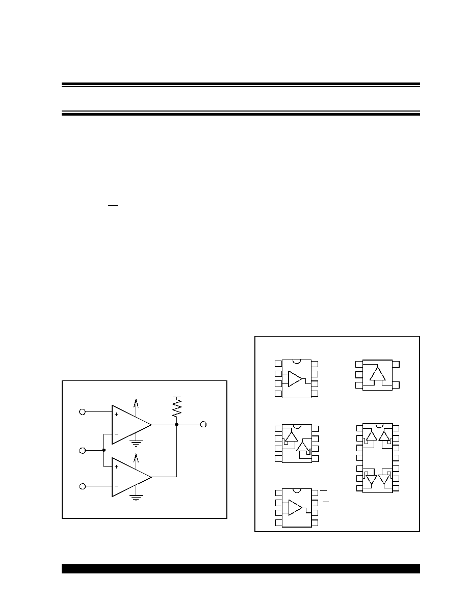
Typical Applications
· Laptop Computers
· Mobile Phones
· Metering Systems
· Hand-held Electronics
· RC Timers
· Alarm and Monitoring Circuits
· Windowed Comparators
· Multi-vibrators
Related Devices
· CMOS/TTL Compatible Output: MCP6541/2/3/4
Typical Application Circuit
Description
The Microchip Technology, Inc. MCP6546/7/8/9 family
of comparators is offered in single (MCP6546), single
with chip select (MCP6548), dual (MCP6547) and quad
(MCP6549) configurations. The outputs are open-drain
and are capable of driving heavy DC or capacitive
loads.
These comparators are optimized for low power, sin-
gle-supply operation with greater than rail-to-rail input
operation. The output limits supply current surges and
dynamic power consumption while switching. The
open-drain output of the MCP6546/7/8/9 family, with a
pull-up resistor, can be used as a level-shifter for any
desired voltage up to 10V, and in wired-OR logic. Input
hysteresis eliminates output switching due to internal
noise voltage, reducing current draw. These compara-
tors operate with a single-supply voltage as low as 1.6V
and draw less than 1 µA/comparator of quiescent
current.
The related MCP6541/2/3/4 family of comparators from
Microchip has a push-pull output that supports rail-to-
rail output swing and interfaces with CMOS/TTL logic.
Package Types
V
RT
MCP654X
MCP654X
V
RB
V
IN
V
PU
R
PU
Windowed Comparator
V
OUT
V
DD
V
DD
+IN
-IN
MCP6546
V
SS
V
DD
OUT
1
2
3
4
8
7
6
5
-
+
NC
NC
NC
PDIP, SOIC, MSOP
4
1
2
3
-
+
5
SOT-23-5, SC-70-5
V
SS
OUT
+IN
V
DD
-IN
MCP6546
MCP6547
+INA
-INA
V
SS
1
2
3
4
8
7
6
5
-
OUTA
+ -
+
V
DD
OUTB
-INB
+INB
+IN
-IN
MCP6548
V
SS
V
DD
OUT
1
2
3
4
8
7
6
5
-
+
NC
CS
NC
PDIP, SOIC, MSOP
PDIP, SOIC, MSOP
MCP6549
+INA
-INA
V
SS
1
2
3
4
14
13
12
11
-
OUTA
+ -
+
V
DD
OUTD
-IND
+IND
10
9
8
5
6
7
OUTB
-INB
+INB
+INC
-INC
OUTC
+
-
-
+
PDIP, SOIC, TSSOP
Open-Drain Output Sub-Microamp Comparators
MCP6546/7/8/9
DS21714B-page 2
2002 Microchip Technology Inc.
1.0
ELECTRICAL
CHARACTERISTICS
1.1
Absolute Maximum Ratings
V
DD
- V
SS
..............................................................7.0V
Open-Drain output..................................... V
SS
+10.5V
All inputs and outputs ........... V
SS
0.3V to V
DD
+0.3V
Difference Input voltage ............................ |V
DD
- V
SS
|
Output Short-Circuit Current .......................continuous
Current at Input Pins .........................................±2 mA
Current at Output and Supply Pins ..................±30 mA
Storage temperature ..........................-65°C to +150°C
Junction Temperature....................................... +150°C
ESD protection on all pins (HBM); (MM) .....4 kV; 200V
Notice: Stresses above those listed under "Maximum Rat-
ings" may cause permanent damage to the device. This is a
stress rating only and functional operation of the device at
those or any other conditions above those indicated in the
operational listings of this specification is not implied. Expo-
sure to maximum rating conditions for extended periods may
affect device reliability.
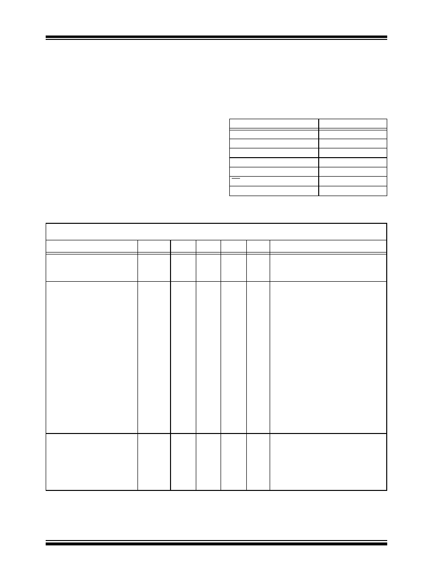
PIN FUNCTION TABLE
DC CHARACTERISTICS
NAME
FUNCTION
+IN/+INA/+INB/+INC/+IND
Non-inverting Inputs
-IN/-INA/-INB/-INC/-IND
Inverting Inputs
V
DD
Positive Power Supply
V
SS
Negative Power Supply
OUT/OUTA/OUTB/OUTC/OUTD Outputs
CS
Chip Select
NC
Not Connected
Electrical Specifications: Unless otherwise indicated, V
DD
= +1.6V to +5.5V, V
SS
= GND, T
A
= 25°C, V
IN+
= V
DD
/2, V
IN-
= V
SS
,
R
PU
= 2.74 k
to V
PU
= V
DD
. Refer to Figure 1-3.
Parameters
Sym
Min
Typ
Max
Units
Conditions
Power Supply
Supply Voltage
V
DD
1.6
--
5.5
V
Quiescent Current per comparator
I
Q
0.3
0.6
1
µA
I
OUT
= 0
Input
Input Voltage Range
V
CMR
V
SS
-0.3
--
V
DD
+0.3
V
Common Mode Rejection Ratio
CMRR
55
70
--
dB
V
DD
= 5V, V
CM
= -0.3V to 5.3V
Common Mode Rejection Ratio
CMRR
50
65
--
dB
V
DD
= 5V, V
CM
= 2.5V to 5.3V
Common Mode Rejection Ratio
CMRR
55
70
--
dB
V
DD
= 5V, V
CM
= -0.3V to 2.5V
Power Supply Rejection Ratio
PSRR
63
80
--
dB
V
CM
= V
SS
Input Offset Voltage
V
OS
-7.0
±1.5
+7.0
mV
V
CM
= V
SS
(Note 1)
Drift with Temperature
V
OS
/
T
--
±3
--
µV/°C T
A
= -40°C to +85°C, V
CM
= V
SS
Input Hysteresis Voltage
V
HYST
1.5
3.3
6.5
mV
V
CM
= V
SS
(Note 1)
Drift with Temperature
V
HYST
/
T
--
10
--
µV/°C T
A
= -40°C to +25°C, V
CM
= V
SS
Drift with Temperature
V
HYST
/
T
--
5
--
µV/°C T
A
= +25°C to +85°C, V
CM
= V
SS
Input Bias Current
I
B
--
1
--
pA
V
CM
=
V
SS
Over Temperature
I
B
--
--
100
pA
T
A
= -40°C to +85°C, V
CM
= V
SS
(Note 3)
Input Offset Current
I
OS
--
±1
--
pA
V
CM
=
V
SS
Common Mode Input Impedance
Z
CM
--
10
13
||4
--
||pF
Differential Input Impedance
Z
DIFF
--
10
13
||2
--
||pF
Open-Drain Output
Output Pull-Up Voltage
V
PU
V
DD
--
10
V
(Note 2)
High-Level Output Current
I
OH
-100
--
--
nA
V
DD
= 1.6V to 5.5V, V
PU
= 10V (Note 2)
Low-Level Output Voltage
V
OL
V
SS
--
V
SS
+0.2
V
I
OUT
= 2 mA, V
PU
= V
DD
= 5V
Short-Circuit Current
I
SC
--
±50
--
mA
V
PU
= V
DD
= 5.0V (Note 2)
Output Pin Capacitance
C
OUT
--
8
--
pF
Note 1: The input offset voltage is the center of the input-referred trip points. The input hysteresis is the difference between the
input-referred trip points.
2: Do not short the output about V
SS
+10V. Limit the output current to Absolute Maximum Rating of 30 mA. The comparator
does not function properly when V
PU
< V
DD
.
3: Input bias current over temperature is not tested for the SC-70-5 package.
2002 Microchip Technology Inc.
DS21714B-page 3
MCP6546/7/8/9
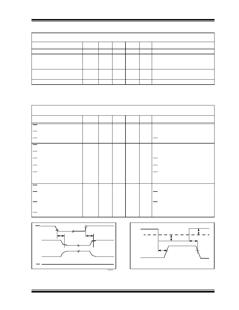
AC CHARACTERISTICS
SPECIFICATIONS FOR MCP6548 CHIP SELECT
FIGURE 1-1:
Timing Diagram for the CS
pin on the MCP6548.
FIGURE 1-2:
Propagation Delay Timing
Diagram.
Electrical Specifications: Unless otherwise indicated, V
DD
= +1.6V to +5.5V, V
SS
= GND, T
A
= 25°C, V
IN+
= V
DD
/2, Step = 200 mV,
Overdrive = 100 mV, R
PU
= 2.74 k
to V
PU
= V
DD
, and C
L
= 36 pF. Refer to Figure 1-2 and Figure 1-3.
Parameters
Sym
Min
Typ
Max
Units
Conditions
Fall Time
t
F
--
0.7
--
µs
(Note 1)
Propagation Delay (High-to-Low)
t
PHL
--
4.0
8.0
µs
Propagation Delay (Low-to-High)
t
PLH
--
3.0
8.0
µs
(Note 1)
Propagation Delay Skew
t
PDS
--
-1.0
--
µs
(Notes 1 and 2)
Maximum Toggle Frequency
f
MAX
--
225
--
kHz
V
DD
= 1.6V
f
MAX
--
165
--
kHz
V
DD
= 5.5V
Input Noise Voltage
E
N
--
200
--
µV
P-P
10 Hz to 100 kHz
Note 1: t
R
and t
PLH
depend on the load (R
L
and C
L
); these specifications are valid for the indicated load only.
2: Propagation Delay Skew is defined as: t
PDS
= t
PLH
- t
PHL
.
Electrical Specifications: Unless otherwise indicated, V
DD
= +1.6V to +5.5V, V
SS
= GND, T
A
= 25°C, V
IN+
= V
DD
/2, V
IN-
= V
SS
,
R
PU
= 2.74 k
to V
PU
= V
DD
, and C
L
= 36 pF. Refer to Figure 1-3.
Parameters
Sym
Min
Typ
Max
Units
Conditions
CS Low Specifications
CS Logic Threshold, Low
V
IL
V
SS
--
0.2V
DD
V
CS Input Current, Low
I
CSL
--
5
--
pA
CS = V
SS
CS High Specifications
CS Logic Threshold, High
V
IH
0.8V
DD
--
V
DD
V
CS Input Current, High
I
CSH
--
1
--
pA
CS = V
DD
CS Input High, V
DD
Current
I
DD
--
18
--
pA
CS = V
DD
CS Input High, GND Current
I
SS
--
-20
--
pA
CS = V
DD
Comparator Output Leakage
I
O(LEAK)
--
1
--
pA
V
OUT
= V
SS
+10V
CS Dynamic Specifications
CS Low to Comparator Output Low
Turn-on Time
t
ON
--
2
50
ms
CS = 0.2V
DD
to V
OUT
= V
DD
/2,
V
IN-
= V
DD
CS High to Comparator Output
High Z Turn-off Time
t
OFF
--
10
--
µs
CS = 0.8V
DD
to V
OUT
= V
DD
/2,
V
IN-
= V
DD
CS Hysteresis
V
CS_HYST
--
0.6
--
V
V
DD
= 5V
V
IL
Hi-Z
t
ON
V
IH
CS
t
OFF
V
OUT
-20 pA, typ.
Hi-Z
I
SS
I
CS
1 pA, typ.
1 pA, typ.
-20 pA, typ.
-0.6 µA, typ.
V
OL
t
PLH
V
OUT
V
IN-
100 mV
100 mV
t
PHL
V
OL
V
IN+
=V
DD
/2
V
OH
MCP6546/7/8/9
DS21714B-page 4
2002 Microchip Technology Inc.
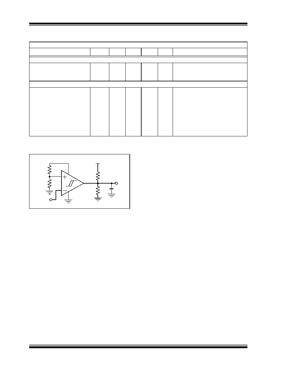
TEMPERATURE SPECIFICATIONS
FIGURE 1-3:
DC Test circuit for the open-
drain output comparators.
Electrical Specifications: Unless otherwise indicated, V
DD
= +1.6V to +5.5V and V
SS
= GND.
Parameters
Sym
Min
Typ
Max
Units
Conditions
Temperature Ranges
Specified Temperature Range
T
A
-40
--
+85
°C
Operating Temperature Range
T
A
-40
--
+125
°C
Note
Storage Temperature Range
T
A
-65
--
+150
°C
Thermal Package Resistances
Thermal Resistance, 5L-SC-70
JA
--
331
--
°C/W
Thermal Resistance, 5L-SOT-23
JA
--
256
--
°C/W
Thermal Resistance, 8L-PDIP
JA
--
85
--
°C/W
Thermal Resistance, 8L-SOIC
JA
--
163
--
°C/W
Thermal Resistance, 8L-MSOP
JA
--
206
--
°C/W
Thermal Resistance, 14L-PDIP
JA
--
70
--
°C/W
Thermal Resistance, 14L-SOIC
JA
--
120
--
°C/W
Thermal Resistance, 14L-TSSOP
JA
--
100
--
°C/W
Note:
The MCP6546/7/8/9 operates over this extended temperature range, but with reduced performance. In any
case, the Junction Temperature (T
J
) must not exceed the Absolute Maximum specification of +150°C.
V
DD
V
SS
= 0V
200 k
200 k
2.74 k
100 k
V
OUT
V
IN
= V
SS
36 pF
MCP654X
R
PU
V
PU
= V
DD
2002 Microchip Technology Inc.
DS21714B-page 5
MCP6546/7/8/9
2.0
TYPICAL PERFORMANCE CURVES
Note: Unless otherwise indicated, V
DD
= +5.0V, V
SS
= GND, T
A
= 25°C, V
IN+
= V
DD
/2, V
IN-
= GND, R
PU
= 2.74 k
to
V
PU
= V
DD
, and C
L
= 36 pF.
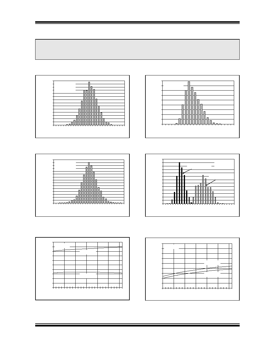
FIGURE 2-1:
Histogram of Input Offset
Voltage with V
CM
= V
SS
.
FIGURE 2-2:
Histogram of Input Offset
Voltage Drift with V
CM
= V
SS
.
FIGURE 2-3:
Input Offset Voltage vs.
Ambient Temperature vs. Power Supply Voltage
with V
CM
= V
SS
.
FIGURE 2-4:
Histogram of Input
Hysteresis Voltage with V
CM
= V
SS
.
FIGURE 2-5:
Histogram of Input
Hysteresis Voltage Drift with Temperature =
-40°C to 25°C and 25°C to 85°C, V
CM
= V
SS
.
FIGURE 2-6:
Input Hysteresis Voltage vs.
Ambient Temperature vs. Power Supply Voltage
with V
CM
= V
SS
.
Note:
The graphs and tables provided following this note are a statistical summary based on a limited number of
samples and are provided for informational purposes only. The performance characteristics listed herein
are not tested or guaranteed. In some graphs or tables, the data presented may be outside the specified
operating range (e.g., outside specified power supply range) and therefore outside the warranted range.
0%
1%
2%
3%
4%
5%
6%
7%
8%
9%
10%
11%
12%
13%
14%
-7 -6 -5 -4 -3 -2 -1 0 1 2 3 4 5 6 7
Input Offset Voltage (mV)
Percentage of Occurrences
1200 Samples
V
CM
= V
SS
0%
1%
2%
3%
4%
5%
6%
7%
8%
9%
10%
11%
12%
13%
14%
15%
-14 -11
-8
-5
-2
1
4
7
10
13
Input Offset Voltage Drift (µV/°C)
Percentage of Occurrences
1200 Samples
V
CM
= V
SS
-500
-400
-300
-200
-100
0
100
200
300
400
500
-40
-20
0
20
40
60
80
Ambient Temperature (°C)
Input Offset Voltage (µV)
V
DD
= 1.6V
V
DD
= 5.5V
V
CM
= V
SS
0%
2%
4%
6%
8%
10%
12%
14%
16%
18%
1.6 2.0 2.4 2.8 3.2 3.6 4.0 4.4 4.8 5.2 5.6 6.0
Input Hysteresis Voltage (mV)
Percentage of Occurrences
1200 Samples
V
CM
= V
SS
0%
2%
4%
6%
8%
10%
12%
14%
16%
18%
20%
22%
24%
26%
2 3 4 5 6 7 8 9 10 11 12 13 14 15 16
Input Hysteresis Voltage Drift (µV/°C)
Percentage of Occurrences
1200 Samples
V
CM
= V
SS
T
A
= -40°C to 25°C
T
A
= 25°C to 85°C
1.5
2.0
2.5
3.0
3.5
4.0
4.5
5.0
5.5
6.0
-40
-20
0
20
40
60
80
Ambient Temperature (°C)
Input Hysteresis Voltage (mV)
V
DD
= 1.6V
V
DD
= 5.5V
V
CM
= V
SS
Document Outline