Passive RFID Device with Sensor Input

2002 Microchip Technology Inc.
DS21308D-page 1
M
MCRF202
Features
· External sensor input
· Data polarity changes with sensor input condition
· Read only data transmission
· 96- or 128-bits of factory programming user mem-
ory (also supports 48 and 64-bit protocols)
· Operates up to 400 kHz carrier frequency
· Low-power operation
· Modulation options:
- ASK, FSK, PSK
· Data Encoding options:
- NRZ Direct, Differential Biphase, Manchester
Biphase
· Die, Wafer, PDIP, or SOIC package option
· Factory programming and device serialization
Applications
· Insect control
· Industrial tagging
Package Type
Description
The MCRF202 is a passive Radio Frequency Identifi-
cation (RFID) device that provides an RF interface for
reading the contents of a user memory array. This
device is specially designed to detect the logic state of
an external sensor, and alters its data transmissions,
based on the condition of the sensor input. The device
outputs a normal bit data stream if the sensor input has
a logic `
1
' state, but outputs an inverted data stream for
a logic `
0
' state. In this way, the reader can monitor the
state (condition) of the external sensor input by detect-
ing whether the data from the device is a normal or
inverted data stream.
The device is powered by rectifying the incoming RF
carrier signal that is transmitted from the reader. When
the device develops sufficient DC voltage, it transmits
the contents of its memory array by modulating the
incoming RF carrier signal. The reader is able to detect
the modulation and decodes the data being transmit-
ted. Code length, modulation option, encoding option,
and bit rate are set at the factory to fit the needs of par-
ticular applications.
The MCRF202 is available in die, wafer, PDIP and
SOIC packages. The encoding, modulation, bit rate
options, and data fields are specified by the customer
and programmed by Microchip Technology Inc. prior to
shipment. See TB023 for more information on factory
serialization (SQTPTM).
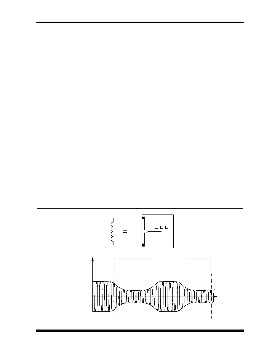
Block Diagram
MCRF202
Reader
RF
Signal
Data
External
Sensor
Switch
PDIP/SOIC
V
A
V
B
1
2
3
4
8
7
6
5
NC
TEST
SENSOR
NC
V
SS
V
CC
Column
V
CC
V
SS
Rectifier and
Clock
Generator
External Coil
and Capacitor
Decode
Row
Decode
Modulation
Control Logic
Counter
Data
Mod
Inverter
Sensor
Input
Circuit
Power-On
Reset
AC Clamp
Connections
V
A
V
B
128-bit
EEPROM
Memory Array
Reset
12-bit
Configuration
Register
Baud
Rate
Timing
Passive RFID Device with Sensor Input

MCRF202
DS21308D-page 2
2002 Microchip Technology Inc.
1.0
ELECTRICAL
CHARACTERISTICS
1.1
Maximum Ratings*
Storage temperature .........................- 65°C to +150°C
Ambient temp. with power applied .....-40°C to +125°C
Maximum current into coil pads..........................50 mA
*Notice: Stresses above those listed under "Maximum rat-
ings" may cause permanent damage to the device. This is a
stress rating only and functional operation of the device at
those or any other conditions above those indicated in the
operational listings of this specification is not implied. Expo-
sure to maximum rating conditions for extended periods may
affect device reliability.
TABLE 1-1:
AC AND DC CHARACTERISTICS
All parameters apply across the
specified operating ranges
unless otherwise noted.
Industrial (I): T
AMB
= -40°C to +85°C
Parameter
Sym
Min
Typ
Max
Units
Conditions
Clock frequency
F
CLK
100
--
400
kHz
Data retention
200
--
--
Years
25°C
Coil current (Dynamic)
I
CD
--
50
--
µ
A
Operating current
with no V
CC
load
I
DD
--
5
--
µ
A
V
CC
= 2V
No load to V
CC
pad
Operating current
with V
CC
load
I
DL
--
10
--
µ
A
V
CC
= 2V
V
CC
load through switch
to sensor
Turn-on-voltage (Dynamic) for
modulation
V
A
V
B
10
--
--
V
PP
V
CC
2
--
--
V
DC
Input Capacitance
C
IN
--
2
--
pF
Between V
A
and V
B
SENSOR pull-down
R
S
400
800
1200
k
SENSOR trigger threshold
V
S
0.5
1.0
1.5
V
2002 Microchip Technology Inc.
DS21308D-page 3
MCRF202
2.0
FUNCTIONAL DESCRIPTION
The device contains three major building blocks. They
are RF front-end and sensor input, configuration and
control logic, and memory sections. The Block Diagram
is shown on page 1.
2.1
RF Front-End and Sensor Input
The RF front-end of the device includes circuits for rec-
tification of the carrier, V
DD
(operating voltage), and
high-voltage clamping to prevent excessive voltage
from being applied to the device. This section also gen-
erates a system clock from the incoming carrier signal
and modulates the carrier signal to transmit data to the
reader.
2.1.1
RECTIFIER AC CLAMP
The AC voltage generated by the external tuned LC cir-
cuit is full wave rectified. This unregulated voltage is
used as the maximum DC supply voltage for the rest of
the device and for the V
CC
supply to the external sen-
sor or switch. Any excessive voltage on the tuned cir-
cuit is clamped by the internal circuitry to a safe level to
prevent damage to the IC.
2.1.2
MODULATION CIRCUIT
The MCRF202 sends the encoded data to the reader
by AM-modulating the coil voltage across the tuned LC
circuit. A modulation transistor is placed between the
antenna coil pads (V
A
and V
B
). The transistor turns on
and off based on the modulation signal. As a result, the
amplitude of the antenna coil voltage varies with the
modulation signal. See Figure 2-1 for details.
2.1.3
V
CC
REGULATOR
The device generates a DC supply voltage from the
unregulated coil voltage.
2.1.4
CLOCK GENERATOR
This circuit generates a clock based on the carrier fre-
quency from the reader. This clock is used to derive all
timing in the MCRF202, including the baud rate and
modulation rate.
2.1.5
POWER-ON RESET
This circuit generates a power-on reset when the tag
first enters the interrogator field. The reset releases
when sufficient power has developed on the V
DD
regulator to allow correct operation.
2.1.6
SENSOR INPUT AND DATA
INVERTER
The SENSOR input responds to logic high or logic low
voltages to drive the internal inverter on or off. A logic
high results in normal tag operation; a logic low at SEN-
SOR input activates an inverter, which inverts the entire
data stream prior to modulation.
The SENSOR input has an internal pull-down resistor
of 800 k
(
typical
)
. See Figure 2-4 for application
details.
FIGURE 2-1:
MODULATION SIGNAL AND MODULATED SIGNAL
MCRF202
Mod.
Signal
V
A
V
B
Mod. TR
Modulation Signal
Modulated Signal
(across V
A
and V
B
)
L
C
Amplitude
t
MCRF202
DS21308D-page 4
2002 Microchip Technology Inc.
2.2
Configuration Register and
Control Logic
The configuration register determines the operational
parameters of the device. It directly controls logic
blocks which generate the baud rate, memory size,
encoded data, modulation protocol, etc. CB11 is
always a zero. Once the array is successfully pro-
grammed at the factory, the lock bit CB12 is set. When
the lock bit is set, programming and erasing the device
becomes permanently disabled. Table 2-1 contains a
description of the control register bit functions.
2.2.1
BAUD RATE TIMING OPTION
The chip will access data at a baud rate determined by
bits CB2, CB3, and CB4 of the configuration register.
For example, MOD32 (CB2 = 0, CB3 = 1, CB4 = 1) has
32 RF cycles per bit. This gives the data rate of 4 kHz
for the RF carrier frequency of 128 kHz.
2.2.2
DATA ENCODING OPTION
This logic acts upon the serial data being read from the
EEPROM. The logic encodes the data according to the
configuration bits CB6 and CB7. CB6 and CB7 deter-
mine the data encoding method. The available choices
are:
· Non-return to zero-level (NRZ_L)
· Biphase_S (Differential)
· Biphase_L (Manchester)
· Inverted Manchester
2.2.3
MODULATION OPTION
CB8 and CB9 determine the modulation protocol of the
encoded data. The available choices are:
· ASK
· FSK
· PSK_1
· PSK_2
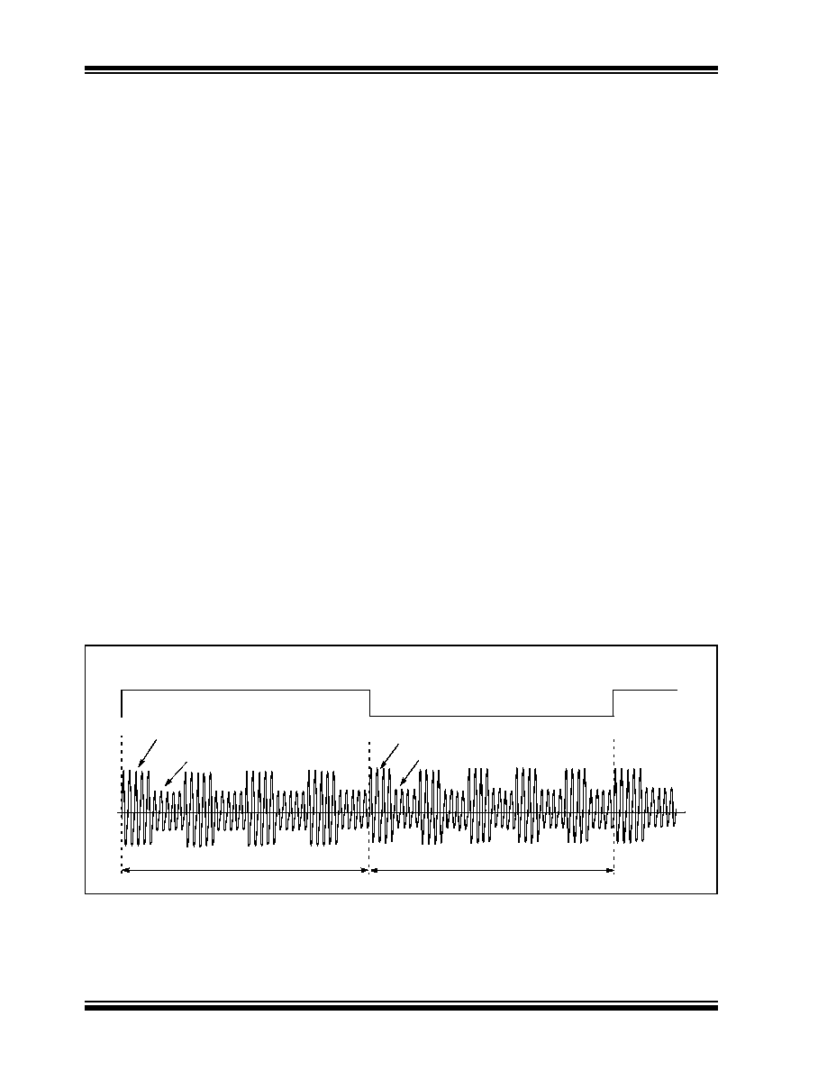
When ASK (direct) option is chosen, the encoded data
is fed into the modulation transistor without change.
When FSK option is chosen, the encoded data is rep-
resented by:
a.
Sets of 10 RF carrier cycles (first 5 cycles
higher amplitude, the last 5 cycles
lower
amplitude) for logic "high" level.
b.
Sets of 8 RF carrier cycles (first 4 cycles
higher amplitude, the last 4 cycles
lower
amplitude) for logic "low" level.
For example, FSK signal for MOD40 is represented:
a.
4 sets of 10 RF carrier cycles for data `
1
'.
b.
5 sets of 8 RF carrier cycles for data `
0
'.
Refer to Figure 2-2 for the FSK signal with MOD40
option.
The PSK_1 represents change in the phase of the
modulation signal at the change of the encoded data.
For example, the phase changes when the encoded
data is changed from `
1
' to `
0
', or from `
0
' to `
1
'.
The PSK_2 represents change in the phase at the
change on `
1
'. For example, the phase changes when
the encoded data is changed from `
0
' to `
1
', or from `
1
'
to `
1
'.
FIGURE 2-2:
ENCODED DATA AND FSK OUTPUT SIGNAL FOR MOD40 OPTION
Encoded Data "1"
Encoded Data "0"
40 RF cycles
40 RF cycles
5 cycles (HI)
5 cycles (LO)
4 cycles (HI)
4 cycles (LO)
2002 Microchip Technology Inc.
DS21308D-page 5
MCRF202
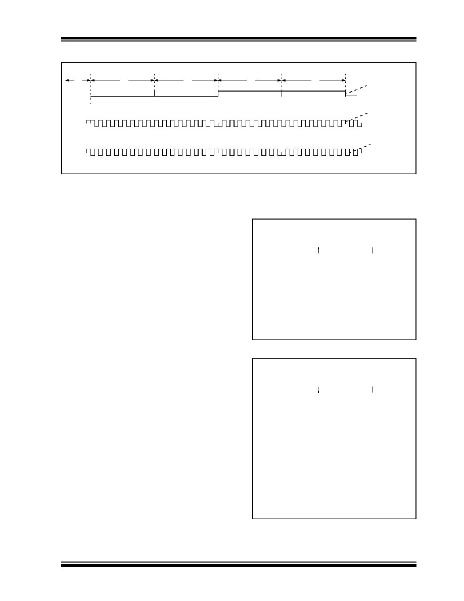
FIGURE 2-3:
PSK DATA MODULATION
2.2.4
MEMORY ARRAY LOCK BIT (CB12)
The CB12 bit must be a `
1
' for a factory programmed
device.
2.3
Memory Section
The device has 128 bits of one-time-programmable
(OTP) memory. The user can choose 96 or 128 bits by
selecting the CB1 bit in the configuration register. See
Table 2-1 for more details.
2.3.1
COLUMN AND ROW DECODER
LOGIC AND BIT COUNTER
The column and row decoders address the EEPROM
array at the clock rate and generate a serial data
stream for modulation. This data stream can be up to
128 bits in length. The size of the data stream is user
programmable with CB1 and can be set to 96 or 128
bits. Data lengths of 48 and 64 bits are available by pro-
gramming the data twice in the array, end-to-end.
The column and row decoders route the proper voltage
to the array for programming and reading. In the pro-
gramming modes, each individual bit is addressed seri-
ally from bit 1 to bit 128.
2.4
Examples of Configuration
Settings
EXAMPLE 2-1:
"88D" Configuration
EXAMPLE 2-2:
"80A" Configuration
P
P
P P
P P
P P
P P
P P
`
0
'
`
0
'
`
1
'
`
1
'
Encoded Data
PSK_ 1
Change on Data
PSK _2
Change on `1'
(NRZ_L)
`
1
'
The "88D" (hex) configuration is interpreted as
follows:
Referring to Table 2-1, the "88D" configuration
represents:
Modulation = PSK_1
PSK rate = rf/2
Data encoding = NRZ_L (direct)
Baud rate = rf/32 = MOD32
Memory size: 128 bits
Programmed device
"88D"
1000-1000-1101
CB12
CB1
The "80A" (hex) configuration is interpreted as
follows:
The MSB corresponds to CB12 and the LSB
corresponds to CB1 of the configuration register.
Therefore, we have:
Referring to Table 2-1, the "80A" configuration
represents:
Programmed device, FSK protocol, NRZ_L
(direct) encoding, MOD50 (baud rate = rf/50),
96 bits.
CB12=1
CB11=0
CB10=0
CB9=0
CB8=0
CB7=0
CB6=0
CB5=0
CB4=1
CB3=0
CB2=1
CB1=0
"80A"
1000-0000-1010
CB12
CB1
Document Outline