 | –≠–ª–µ–∫—Ç—Ä–æ–Ω–Ω—ã–π –∫–æ–º–ø–æ–Ω–µ–Ω—Ç: MCRF451/S | –°–∫–∞—á–∞—Ç—å:  PDF PDF  ZIP ZIP |
MCRF450/451/452/455 13.56 MHz Read/Write Passive RFID Device Data Sheet
2003 Microchip Technology Inc.
DS40232G-page 1
MCRF450/451/452/455
Features
∑ Contactless read and write with anticollision
algorithm
∑ 1024 bits (32 blocks) of total memory
∑ 928 bits (29 blocks) of user programmable
memory
∑ Unique 32-bit tag ID (factory programmed)
∑ 32 bits for data and 16 bits for CRC per block
∑ Block write-protection
∑ 70 Kbit/s read data rate (Manchester format)
∑ Special bit (Fast Read) for fast identification and
anti-counterfeit applications (EAS)
∑ 1-of-16 PPM encoding for writing data
∑ Interrogator-Talks-First (ITF) or Tag-Talks-First
(TTF) operation
∑ Long range for reading and writing
∑ High speed anticollision algorithm for reading and
writing
∑ Fast and Normal modes for write data speed
∑ Anti-tearing feature for secure write transactions
∑ Asynchronous operation for low power consump-
tion and flexible choice of carrier frequency bands
∑ Internal resonance capacitors
(MCRF451/452/ 455)
∑ Two pad connections for external antenna circuit
(MCRF452)
∑ Three pad connections for external antenna
circuit (MCRF450, 451, 455)
∑ Very low power CMOS design
∑ Die in waffle pack, wafer, wafer on frame, bumped
wafer, COB, PDIP or SOIC package options
Applications
∑ Item Level Tagging: To read and write multiple
items in long read range environment.
∑ Anti-Counterfeit: The device has a unique
feature to distinguish between paid, unpaid or
returned merchandise.
∑ Inventory Management: Tag's data can be read
or updated (written) in multiple tags and long
range environment. Its memory (32 blocks, 1 Kbit,
each block = 32 bits) is well organized for the
inventory management applications.
∑ Product Identifications
∑ Airline Baggage Tracking
∑ Book Store and Library Book ID
∑ Low Cost Animal Ear Tags: The device's long
range reading performance combined with 1 Kbit
of memory is suitable for animal tagging applica-
tions. Tag cost can be cheaper and read range is
much longer than existing 125 kHz conventional
animal ear tags.
∑ Toys and Gaming Tools: Device's anticollision
feature for reading and writing allows to make
intelligent interactive toys and gaming tools.
∑ Access Control and Time Attendance Cards:
Device's long range performance allows to make
long range access control, parking lot entry, and
time attendance cards.
Inexpensive finished tags and readers are available
from Microchip's worldwide OEM partners. Please
contact Microchip Technology Inc. near you or visit
http://www.microchip.com for further product
information and inquiries for your applications.
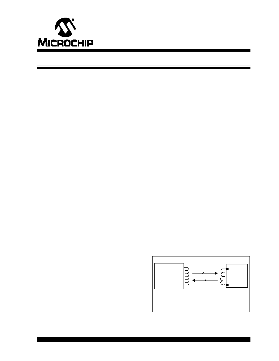
Typical Configuration for Applications
Command and Data
Read/Write
Data
Interrogator
MCRF452
(Reader/Writer)
Ant. A
V
SS
Read/Write Range:~ up to 1.5 meters depending
on tag size and system
requirements.
13.56 MHz Read/Write Passive RFID Device
MCRF450/451/452/455
DS40232G-page 2
2003 Microchip Technology Inc.
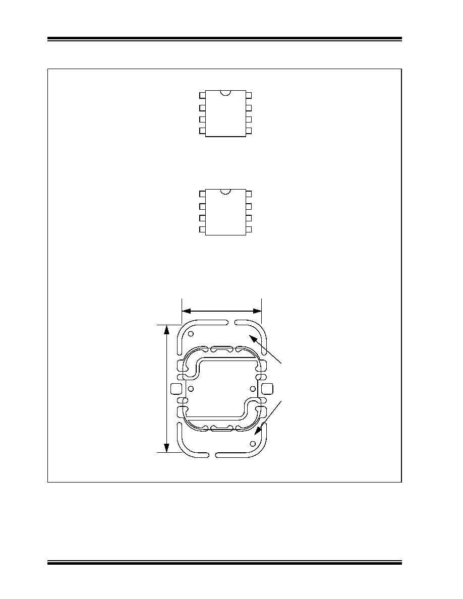
Package Types
PDIP ("P")
ANT. A
V
DD
1
2
3
4
8
7
6
5
NC
ANT. B
CLK
F
CLK
NC
V
SS
Note: Pins 4, 7 and 8 are for device test purposes only
MCRF450/451/455: Antenna connections = pins 1, 3 and 5
MCRF452: Antenna connections = pins 1 and 5
ROTATED SOIC ("X/SN")
ANT.B
V
DD
1
2
3
4
8
7
6
5
NC
CLK
F
CLK
NC
V
SS
Note: Pins 3, 5 and 7 are for device test purposes only
MCRF450/451/455: Antenna connections = pins 1, 4 and 8
MCRF452: Antenna connections = pins 4 and 8
ANT. A
NC = Not Connected
NC = Not Connected
5 mm
8m
m
Thickness = 0.4 mm
Antenna Coil Connection
MCRF450 COB ("7M")

2003 Microchip Technology Inc.
DS40232G-page 3
MCRF450/451/452/455
1.0
DESCRIPTION OF DEVICE
FEATURES
The MCR45X is a contactless read/write passive RFID
device that is optimized for 13.56 MHz RF carrier
signal. The device needs an external LC resonant
circuit to communicate wirelessly with the Interrogator.
The device is powered remotely by rectifying an RF
signal that is transmitted from the Interrogator and
transmits or updates its contents from memory-based
on commands from the Interrogator.
The device is engineered to be used effectively for item
level tagging applications, such as retail and inventory
management, where a large volume of tags are read
and written in the same Interrogator field.
The device contains 32 blocks (B0 - B31) of EEPROM
memory. Each block consists of 32 bits. The first three
blocks (B0 - B2) are allocated for device operation,
while the remaining 29 blocks (B3 - B31: 928 bits) are
for user data. Block 1 contains unique 32 bits of Tag ID.
The Tag ID is preprogrammed at the factory and write
protected.
All blocks, except for the Tag ID (block 1), are contact-
lessly writable block-wise by Interrogator commands.
All data blocks, with the exception of bits 30 and 31 in
block 0, are write-protectable.
The device can be configured as either Tag-Talks-First
(TTF) or Interrogator-Talks-First (ITF). In TTF mode,
the device transmits its fast response data (160 bits
max., see Example 9-1) as soon as it is energized, then
waits for the next command. In ITF mode, the device
requires an Interrogator command before it sends any
data. The control bits for TTF and ITF modes are bits
30 and 31 in block 0.
All downlink commands from the Interrogator are
encoded using 1-of-16 Pulse Position Modulation
(PPM) and specially timed gap pulses. This encoded
information amplitude modulates the Interrogator's RF
carrier signal.
At the other end, the MCR45X device demodulates the
received RF signal and then sends data (from memory)
at 70 Kbit/s back to the Interrogator in Manchester
format.
The communication between Interrogator and device
takes place asynchronously. Therefore, to enhance the
detection accuracy of the device, the Interrogator
sends a time reference signal (time calibration pulse) to
the device, followed by the command and program-
ming data. The time reference signal is used to
calibrate timing of the internal decoder of the device.
There are device options for the internal resonant
capacitor between antenna A and V
SS
: (a) no internal
resonant capacitor for the MCRF450, (b) 100 pF for the
MCRF451, (c) two 50 pF in series (25 pF in total) for the
MCRF452 and (d) 50 pF for the MCRF455. The internal
resonant capacitors for each device are shown in
Figures 2-2 through 2-5.
The MCRF450 needs an external LC resonant circuit
connected between antenna A, antenna B and V
SS
pads. See Figure 2-2 for the external circuit configura-
tion. The MCRF452 needs a single external antenna
coil only between antenna A and V
SS
pads, as shown
in Figure 2-4.
This external circuit, along with the internal resonant
capacitor, must be tuned to the carrier frequency of the
Interrogator for maximum performance.
When a tag (device with the external LC resonant
circuit) is brought to the Interrogator's RF field, it
develops an RF voltage across the external circuit. The
device rectifies the RF voltage and develops a DC
voltage (V
DD
). The device becomes functional as soon
as V
DD
reaches the operating voltage level.
The device then sends data stored in memory to the
Interrogator by turning on/off the internal modulation
transistor. This internal modulation transistor is located
between antenna B and V
SS
. The modulation transis-
tor has a very small turn-on resistance between Drain
(antenna B) and Source (V
SS
) terminals during its turn-
on time.
When the modulation transistor turns on, the resonant
circuit component between antenna B and V
SS
, which
is in parallel with the modulation transistor, is shorted
due to the low turn-on resistance. This results in a
change in the LC value of the circuit. As a result, the cir-
cuit no longer resonates at the carrier frequency of the
Interrogator. Therefore, the voltage across the circuit is
minimized. This condition is called "cloaking".
When the modulation transistor turns off, the circuit
resonates at the carrier frequency of the Interrogator
and develops maximum voltage. This condition is
called "uncloaking". Therefore, the data is sent to the
Interrogator by turning on (cloaking) and off (uncloak-
ing) the modulation transistor.
The voltage amplitude of the carrier signal across the
LC resonant circuit changes depending on the
amplitude of modulation data. This is called an ampli-
tude modulation signal. The receiver channel in the
Interrogator detects this amplitude modulation signal
and reconstructs the modulation data for decoding.
The device includes a unique anticollision algorithm to
be read or written effectively in multiple tag environ-
ments. To minimize data collision, the algorithm utilizes
time division multiplexing of the device response. Each
device can communicate with the Interrogator in a
different time slot. The devices in the Interrogator's RF
field remain in a nonmodulating condition if they are not
in the given time slot. This enables the Interrogator to
communicate with the multiple devices one at a time
without data collision. The details of the algorithm are
described in Section 6.0, "Read/Write Anticollision
Logic".

MCRF450/451/452/455
DS40232G-page 4
2003 Microchip Technology Inc.
To enhance data integrity for writing, the device
includes an anti-tearing feature. This anti-tearing
feature provides verification of data integrity for incom-
plete write cycles due to failed communication between
the Interrogator and the device during the write
sequences.
1.1
Device's Communication with
Interrogator
The device can be operated in either Fast Read
Request (FRR) or Fast Read Bypass (FRB) mode,
depending on the status of bit 31 (FR: bit) of block 0. If
the FR bit is set, the device is operated in FRR mode,
and FRB mode, if the FR bit is cleared. The FR bit is
always reprogrammable and not write protectable. The
FRR mode is a default setting. The communication
between the Interrogator and tag starts with a FRR or
FRB command.
In FRR mode, the device sends a response only when
it receives the FRR command, not the FRB command.
Conversely, the device in FRB mode sends a response
when it receives the FRB command only, not the FRR
command.
If the device is set to FRR mode and also set to TTF
mode (TF bit = set), the device can send the FRR
response as soon as it is energized.
One of the main purposes of using the two different
modes (FRR and FRB) is to use the device effectively
in the item level supply-chain application, where a rapid
identification and an effective anticollision read/write
process is needed (i.e., to identify whether it is a paid
or unpaid item, or whether it passed one particular point
of interest or not). This can be done by either checking
the status of the FR bit or by checking the response of
the tag to the command. For this reason, the FR bit is
also called an Electronic Article Surveillance (EAS) bit.
1.1.1
OPERATION OF TAG IN FRR MODE
If the device is in the FRR mode (FR bit = set), the
communication between the Interrogator and the
device can start in two ways, depending on the status
of TF (Bit 30 of block 0). If the TF bit is cleared, it is
called ITF mode. In this case, the tag waits for the Inter-
rogator's FRR command and sends the FRR response
data when it sees the FRR command. If the TF bit is
set, the device is in a TTF mode. In this case, the tag
sends the FRR response as soon as it is energized,
even without the FRR command. The tag has a short
listening window (1 ms) immediately after the FRR
response. The Interrogator sends its next command
during this listening window.
The FRR response includes the 32 bits of tag ID and
FRF (Blocks 3 -5). See Tables 7-3, 7-4 and 7-6 for
data. The Interrogator identifies which tags are in the
field by receiving their FRR responses.
Based upon the FRR response, the Interrogator will
send Matching code 1 (MC1) or Matching code 2
(MC2) during the tag's listening window. The Interroga-
tor sends the MC1 to put the tag into SLEEP mode.
Tags in SLEEP mode never respond to any command.
Removal of the Interrogator's RF energy from the
device is the only way to wake-up the device.
If the tag needs further read/write processing, the
Interrogator sends the MC2, followed by a Read or
Write command. After the completion of reading or
writing of block data, the Interrogator sends an End
command to put the tag into SLEEP mode.
The reading and writing of the FRR devices takes place
in the Anticollision mode. For instance, if there are mul-
tiple tags in the field, the Interrogator selects one tag at
a time by controlling the tag's time slot for the FRR
response. The Interrogator repeats this sequence until
all tags in its field are processed:
- send FRR command
- receive FRR response
- send Matching code 1 or 2 at tag's listing window
- send Read Block command/or send Write
Block command and data
- verify read/write response
- send End command
- verify the End command response
- look for other tag's FRR responses
1.1.2
OPERATION OF TAG IN FRB MODE
The communication with the device in the FRB mode is
initiated by the FRB command only. If the device sees
the Interrogator's FRB command, it sends its 32-bit tag
ID and waits for the MC2. This is followed by a Read or
Write command. Once the device is read or written, the
Interrogator sends an End command. Unlike the FRR
mode, the reading and writing of the tag are processed
in a non Anticollision mode.
See Section 6.0, "Read/Write Anticollision Logic", for
the read and write anticollision algorithm. See
Example 9-1 for command sequences and device
responses.
2003 Microchip Technology Inc.
DS40232G-page 5
MCRF450/451/452/455
2.0
ELECTRICAL
CHARACTERISTICS
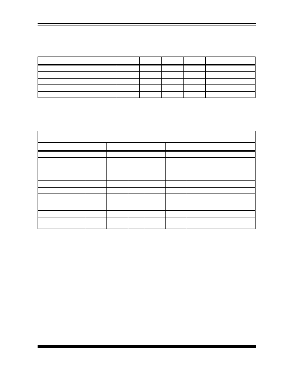
TABLE 2-1:
ABSOLUTE RATINGS
TABLE 2-2:
OPERATING DC CHARACTERISTICS
Parameters
Symbol
Min
Max
Units
Conditions
Coil current into coil pad
I
PP
_
AC
--
40
mA
Peak-to-Peak coil current
Maximum power dissipation
P
MPD
--
0.5
W
--
Ambient temperature with power applied
T
AMB
-40
+125
∞C
--
Assembly temperature
T
ASM
--
300
∞C
< 10 sec.
Storage temperature
T
STORE
-65
150
∞C
--
Note:
Stresses above those listed under "Maximum ratings" may cause permanent damage to the device. This is
a stress rating only and functional operation of the device at those or any other conditions above those
indicated in the operational listings of this specification is not implied. Exposure to maximum rating
conditions for extended periods may affect device reliability.
Standard Operating Conditions (unless otherwise stated)
Operating Temperature = -20∞C to +70∞C
Parameters
Symbol
Min
Typ
Max
Units
Conditions
Reading voltage
V
DDR
2.8
--
--
V
V
DD
voltage for reading at 25∞C
Operating current in
Normal mode
I
OPER
_
N
--
20
--
µA
V
DD
= 2.8V during reading at 25∞C
Operating current in
Fast mode
I
OPER
_
F
--
45
--
µA
V
DD
= 2.8V during reading at 25∞C
Writing current
I
WRITE
--
130
--
µA
At 25∞C, V
DD
= 2.8V
Writing voltage
V
WRITE
2.8
--
--
V
DC
At 25 ∞C
Modulation resistance
R
M
--
3.0
5.0
DC turn-on resistance between
Drain and Source terminals of the
modulation transistor at V
DD
= 2.8V
Data retention
--
200
--
--
Years
For T < 120∞C
Endurance
--
1.0
--
--
Million
Cycles
At 25∞C
Document Outline
- 1.0 Description of Device Features
- 2.0 Electrical Characteristics
- 3.0 Block Diagram
- 4.0 Analog Front-End
- 5.0 Detection And Encoding
- 6.0 Read/Write Anticollision Logic
- TABLE 6-1: conditions for tcmax = elapsed for itf mode�
- 6.1 Description of Algorithm
- FIGURE 6-1: anticollision flow chart�
- TABLE 6-2: read/write commands from interrogator to device�
- TABLE 6-3: interrogator commands and device responses��
- TABLE 6-4: specification of gap signal for FRR and FRB commands��
- TABLE 6-5: specification OF modulation sequence for frr COMMAND��
- TABLE 6-6: specification of modulation sequence for frb command�
- FIGURE 6-2: pulse waveform of gap and 1-of-16�ppm signals�
- TABLE 6-7: waveform characteristics of gap and 1-of-16�ppm signals�
- FIGURE 6-3: gap modulation patterns for frr, normal speed, tsmax = 1�
- FIGURE 6-4: gap modulation patterns for frr, fast speed, tsmax = 1�
- FIGURE 6-5: gap modulation patterns for frr, normal speed, tsmax = 16�
- FIGURE 6-6: gap modulation patterns for frr, fast speed, tsmax = 16�
- FIGURE 6-7: gap modulation patterns for frr, tsmax = 64, TCMAX = 1�
- FIGURE 6-8: gap modulation patterns for frB (fast request bypass)�
- TABLE 6-8: frr command repeat time vs. (tsmax, tcmax)�
- TABLE 6-9: 1-of-16�ppm pulse specifications�
- FIGURE 6-9: 1-0f-16�ppm representation for hex values for normal speed mode�
- FIGURE 6-10: calibration pulses for normal speed mode�
- TABLE 6-10: example: tag id = h¥825fe1a0��
- 7.0 Memory Section
- 8.0 Device Testing
- 9.0 Examples
- 10.0 Failed Die Identification
- 11.0 Wafer Delivery Documentation
- 12.0 Notice On Die And Wafer Handling
- 13.0 References
- 14.0 Packaging Information
- On-Line Support
- Systems Information and Upgrade Hot Line
- Reader Response
- Product Identification System
- Trademarks
- Worldwide Sales