 | –≠–ª–µ–∫—Ç—Ä–æ–Ω–Ω—ã–π –∫–æ–º–ø–æ–Ω–µ–Ω—Ç: MTE1122IP | –°–∫–∞—á–∞—Ç—å:  PDF PDF  ZIP ZIP |

©
1995 Microchip Technology Inc.
Preliminary
DS21112B-page 1
FEATURES
∑ Energy Management Controller
∑ Based on 8-bit RISC Technology
∑ Proprietary Power Management Algorithm
∑ Reduces the power consumption of induction
motor systems
∑ 5V Operation
∑ 18-pin PDIP and SOIC Packages
∑ 8-bit Analog-to-Digital (A/D) Converter
∑ Automatic Power-on Reset
∑ Power-up Timer
∑ Commercial and Industrial Temperature Range
Operation
∑ Multiple parts can be slaved for three-phase oper-
ation
INTRODUCTION
The MTE1122 is an Energy Management Controller IC
for single-phase induction motors. This CMOS device
is based on Microchip Technology Inc's RISC proces-
sor core and proprietary algorithms. When combined
with some external analog components, it will provide
an electronic system that economically reduces the
operating costs of small induction motors by as much
as 58%. It will also allow motors to run cooler and with
less vibration. The system operates on single phase
110 or 220 VAC.
PACKAGE TYPE
FIGURE 1: SYSTEM BLOCK DIAGRAM
V
SS
1
P-Sense
V
SS
RESET
V
SS
ZC-Sense
TTRIG
NC
NC
∑
1
2
3
4
5
6
7
8
9
V
SS
Gate Input
OSC1
OSC2
V
DD
IND
NC
NC
NC
18
17
16
15
14
13
12
11
10
M
T
E1
122
18-Lead PDIP/SOIC
MTE1122
LINE IN
LINE OUT
TO MOTOR
TRIAC
VOLTAGE
ZERO-CROSS
VOLTAGE AMP
CURRENT
ZERO-CROSS
V
CC
POWER
NEUTRAL IN
NEUTRAL OUT
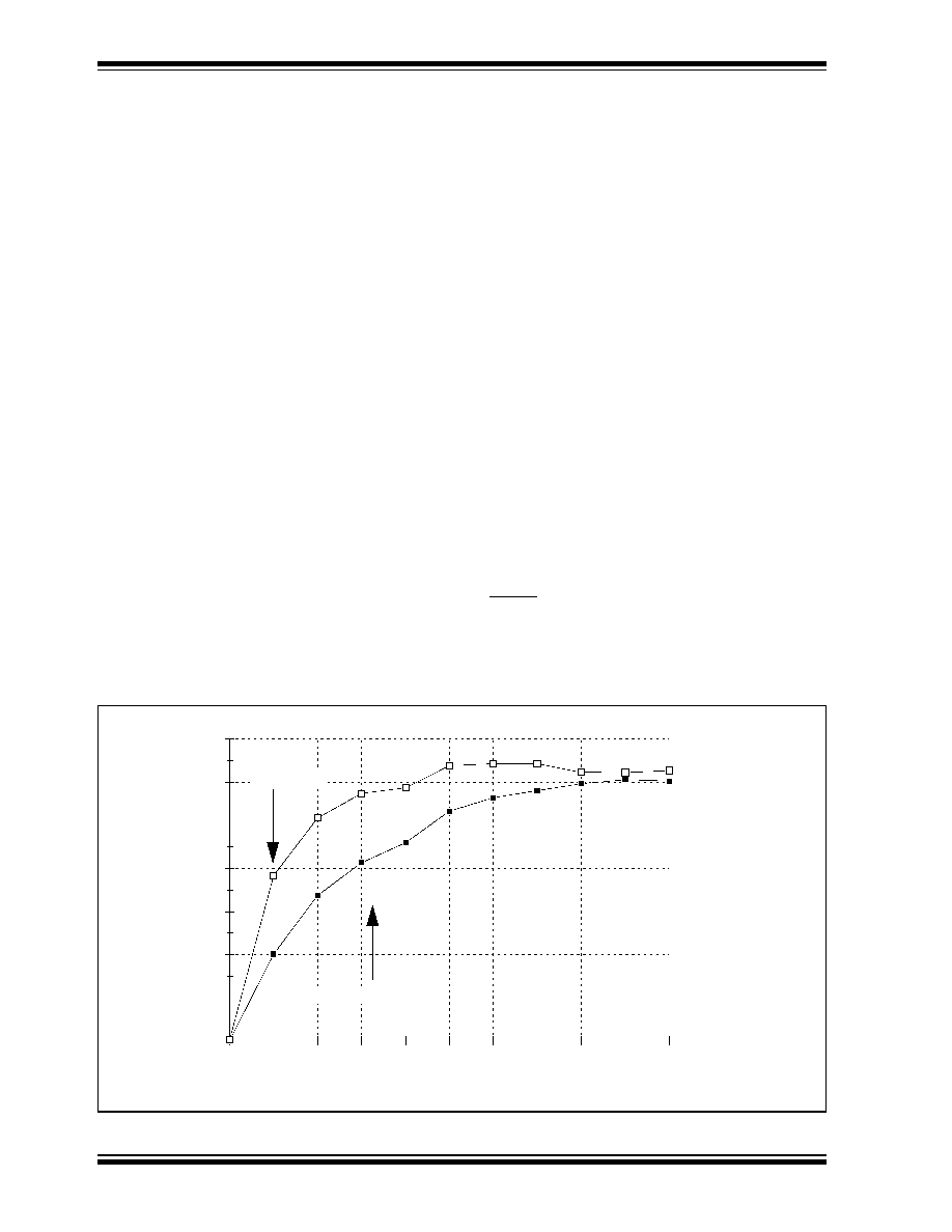
FIGURE 2: ENERGY SAVINGS
0 . 0
10.0
20.0
30.0
40.0
50.0
60.0
0
1 0
2 0
3 0
4 0
5 0
6 0
7 0
8 0
9 0
1 0 0
P
e
r
c
ent Sa
vin
g
s
Percent Load
MTE1122
Energy Management Controller IC
MTE1122
DS21112B-page 2
Preliminary
©
1995 Microchip Technology Inc.
FUNCTIONAL DESCRIPTION
Single-phase induction motors run most efficiently at
full load. As the applied load lessens, a greater portion
of the energy consumed by the motor is wasted, mostly
as heat.
It is estimated by the EPA that 50% of the energy pro-
duced in the US is consumed by small electric motors,
and that 20% of this energy does no useful work. There
are perhaps three major reasons for this:
1.
Over-specification -- sometimes its easier or
costs no more to specify a larger motor than
determine actual loads.
2.
Worst case design -- pumps, conveyers, fans,
and the like must be able to operate properly
with clogged filters, maximum heads, or speci-
fied loads. If filters are clean, or loads are lower,
the motor will be running only partly loaded.
3.
Idle time -- many times, systems can't be shut
down conveniently when not in use.
Number 1 above can be corrected by proper design.
For example, in modern refrigerators, the compressor
systems have been optimized quite effectively. Num-
bers 2 and 3 can not be improved using traditional
approaches. This is where the MTE1122 provides a
new, cost-effective solution.
The MTE1122 calculates the amount of load on a motor
connected to it, and adjusts the motor's supply voltage
to match that load. For example, if the load is lower
than the motor's rated load, the voltage to the motor
can be reduced, thus decreasing the energy used by
the motor.
A 1/3 HP motor will typically see 85 VAC at no load
when powered through the MTE1122, for an energy
savings of as much as 58%.
A system block diagram is shown in Figure 1. A graph
of energy savings vs. motor load is shown in Figure 2.
A graph of motor efficiency with and without an
MTE1122-based energy management controller (EMC)
is shown in Figure 3. The data for the graphs are
shown in Table 1. These figures are based on a 1/3 HP
induction motor coupled to a dynamometer. Actual
savings may vary based on motor size, motor load and
motor construction.
PINOUT DESCRIPTIONS
P-Sense - analog input that is used by the device to
measure the load voltage.
Gate Enable - analog input that monitors the voltage
across the triac. It is used as a current feedback mech-
anism.
IND - TTL-compatible output that indicates that the sys-
tem is operating normally. It is intended to control an
LED or another indicator device.
ZC-Sense - TTL-compatible input that is used to deter-
mine the zero crossing point of the AC voltage wave-
form.
TTRIG - TTL-compatible output that is used to drive the
triac.
RESET - TTL-compatible input used to reset the device
by holding this pin low.
OSC1, OSC2 - Oscillator crystal or resonator connec-
tions.
FIGURE 3: MOTOR EFFICIENCY
0 . 0
10.0
20.0
30.0
40.0
50.0
60.0
70.0
0
1 0
2 0
3 0
4 0
5 0
6 0
7 0
8 0
9 0
1 0 0
E
f
fic
i
ency
Percent Load
With E.M.C.
Without E.M.C.
©
1995 Microchip Technology Inc.
Preliminary
DS21112B-page 3
MTE1122
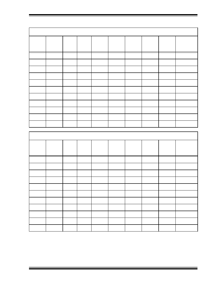
TABLE 1:
OPERATING PARAMTER COMPARISONS
1/3 HP Motor without E.M.C.
Load
(%)
Load
(Nm)
Vrms
Irms
(A)
Power
Factor
Power
In (W)
RPM
Power
Out (W)
Power
Out
(HP)
Efficiency
(%)
0
0.00
115
5.7
0.18
120
1791
0
0.00
0.2
10
0.14
115
5.7
0.20
130
1788
26
0.04
20.1
20
0.29
115
5.7
0.24
160
1781
54
0.07
33.7
30
0.43
115
5.7
0.29
193
1777
80
0.11
41.4
40
0.57
115
5.7
0.35
229
1768
105
0.14
46.0
50
0.72
115
5.8
0.37
249
1764
133
0.18
53.3
60
0.86
115
5.8
0.42
280
1758
158
0.21
56.4
70
1.00
115
6.0
0.46
315
1750
183
0.25
58.0
80
1.14
116
6.1
0.49
348
1744
208
0.28
59.7
90
1.29
115
6.3
0.53
386
1736
234
0.31
60.6
100
1.43
116
6.5
0.57
428
1727
258
0.35
60.3
1/3 HP Motor with E.M.C.
Load
(%)
Load
(Nm)
Vrms
Irms
(A)
Power
Factor
Power
In (W)
RPM
Power
Out (W)
Power
Out
(HP)
Efficiency
(%)
0
0.00
113
3.1
0.14
50
1794
0
0.00
0.4
10
0.14
113
3.2
0.19
68
1786
26
0.04
38.4
20
0.29
113
3.5
0.26
104
1775
54
0.07
51.7
30
0.43
113
3.8
0.32
138
1764
79
0.11
57.4
40
0.57
113
4.1
0.38
178
1755
104
0.14
58.7
50
0.72
113
4.3
0.42
206
1749
132
0.18
63.8
60
0.86
112
4.6
0.47
243
1740
156
0.21
64.3
70
1.00
112
4.9
0.51
281
1730
181
0.24
64.3
80
1.14
112
5.3
0.55
329
1722
205
0.27
62.3
90
1.29
112
5.6
0.59
371
1713
231
0.31
62.2
100
1.43
111
6.0
0.61
406
1705
255
0.34
62.7

MTE1122
DS21112B-page 4
Preliminary
©
1995 Microchip Technology Inc.
ELECTRICAL CHARACTERISTICS
Absolute Maximum Rating
Ambient temperature under bias .................................................................................................................-55 to +125∞C
Storage Temperature.............................................................................................................................. -65∞C to +150∞C
Voltage on any pin with respect to V
SS
(except V
DD
and RESET).................................................... -0.6V to V
DD
+0.6V
Voltage on V
DD
with respect to V
SS
..................................................................................................................0 to +7.5V
Voltage on RESET with respect to V
SS
(Note 1) ................................................................................................0 to +14V
Total power Dissipation (Note 2) ...........................................................................................................................800mW
Max. Current out of V
SS
pin ...................................................................................................................................150mA
Max. Current into V
DD
pin ......................................................................................................................................100mA
Input Clamping Current, IIK (VI<0 or VI>V
DD
)
.................................................................................................................. ±
20mA
Output Clamping Current, IOK (V0<0 or V0>V
DD
)
.......................................................................................................... ±
20mA
Max. Output Current sunk by any I/O pin .................................................................................................................25mA
Max. Output Current sourced by any I/O pin............................................................................................................20mA
Note 1: Voltage spikes below V
SS
at the RESET pin, inducing currents greater than 80mA, may cause latch-up.
Thus, a series resistor of 50-100
should be used when applying a "low' level to the RESET pin rather than
pulling this pin directly to V
SS
.
Note 2: Total power dissipation should not exceed 800 mW for the package. Power dissipation is calculated as fol-
lows:
P
DIS
= V
DD
x {I
DD
-
I
OH
} +
{(V
DD
-V
OH
) x I
OH
} +
(V
OL
x I
OL
)
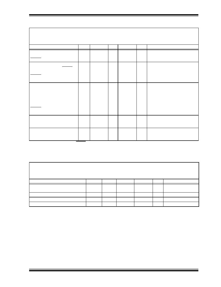
TABLE 2:
DC CHARACTERISTICS POWER SUPPLY PINS
NOTICE: Stresses above those listed under "Maximum Ratings" may cause permanent damage to the device. This
is a stress rating only and functional operation of the device or compliance to AC and DC parametric specifications at
those or any other conditions above those indicated in the operation listings of this specification is not implied. Expo-
sure to maximum rating conditions for extended periods may affect device reliability.
Power Supply Pins
Standard Operating Conditions (unless otherwise stated)
Operating temperature
-40∞C
T
A
+ 85∞C for industrial,
0∞C
T
A
+70∞C for commercial
Operating voltage V
DD
= 4.0V to 6.0V
Characteristic
Sym
Min
Typ
(Note 1)
Max Units
Conditions
Supply Voltage
V
DD
4.0
6.0
V
V
DD
start voltage to guarantee
power on reset
V
POR
Vss
V
V
DD
rise rate to guarantee
Power-On Reset (Note 2)
S
VDD
0.05
V/ms
Supply Current (Note 3)
I
DD
1.8
3.3
mA
F
OSC
= 4 MHz, V
DD
= 5.5V
Note 1: Data in the column labeled "Typical" is based on characterization results at 25
∞
C. This data is for design guidance only and
is not tested for, or guaranteed by Microchip Technology.
2: This parameter is characterized but not tested.
3: The supply current is mainly a function of the operating voltage and frequency. Other factors such as I/O pin loading and
switching rate, oscillator type, internal code execution pattern, and temperature also have an impact on the current con-
sumption.
©
1995 Microchip Technology Inc.
Preliminary
DS21112B-page 5
MTE1122
TABLE 3:
DC CHARACTERISTICS: ALL PINS EXCEPT POWER SUPPLY
TABLE 4:
AC CHARACTERISTICS
All Pins Except Power
Standard Operating Conditions (unless otherwise stated)
Operating temperature
-40∞C
T
A
+ 85∞C for industrial,
0∞C
T
A
+70∞C for commercial
Operating voltage V
DD
= 4.0V to 6.0V
Characteristic
Sym
Min
Typ
Max
Units
Conditions
Input Low Voltage:
All Input Pins (Except OSC1)
RESET OSC1
V
IL
V
IH
V
SS
V
SS
0.2 V
DD
0.3 V
DD
V
V
Input High Voltage:
All Input Pins (Except RESET,
OSC1)
RESET
OSC1
V
IH
V
IH
V
IH
0.36 V
DD
0.85 V
DD
0.7 V
DD
V
DD
V
DD
V
DD
V
V
V
4.5V
V
DD
5.5V
Input Leakage Current:
(Notes 1,2)
IND, TTRIG, AC-Sense
P-Sense, Gate Input
RESET
OSC1
I
IL
±1
±1
±1
±1
µ
A
µ
A
µ
A
µ
A
V
SS
V
PIN
V
DD
,
Pin at hi-impedance
V
SS
V
PIN
V
DD
,
Pin at hi-impedance
V
SS
V
PIN
V
DD
V
SS
V
PIN
V
DD
Output Low Voltage:
All Output Pins
V
OL
0.6
V
I
OL
= 8.5mA, V
DD
= 4.5V,
-40
∞
C to +85
∞
C
Output High Voltage:
All Output Pins (Note 2)
V
OH
0.7 V
DD
V
I
OH
83.mA, V
DD
= 4.5V,
-40
∞
C to +85
∞
C
Note 1: The leakage current on the RESET pin is strongly dependent on the applied voltage level. The specified levels represent
normal operating conditions. Higher leakage current may be measured at different input voltages.
2: Negative current is defined as current coming out of the pin.
AC Characteristics
Standard Operating Conditions (unless otherwise stated)
Operating temperature
-40∞C
T
A
+ 85∞C for industrial,
0∞C
T
A
+70∞C for commercial
Operating voltage V
DD
= 4.0V to 6.0V
Characteristic
Sym
Min
Typ
Max
Units
Conditions
Oscillator Frequency
F
OSC
4
4
MHz
Clock in (OSC1) High or Low Time
T
CKHLXT
50
ns
Note
1
Clock in (OSC1) Rise or Fall Time
TCKRFXT
25
ns
Note 1
RESET Pulse Width (low)
T
MCL
200
ns
Note 1