©
1999 Microchip Technology Inc.
Preliminary
DS41106A-page 1
Devices included in this Data Sheet:
· PIC16C712
· PIC16C716
Microcontroller Core Features:
· High-performance RISC CPU
· Only 35 single word instructions to learn
· All single cycle instructions except for program
branches which are two cycle
· Operating speed: DC - 20 MHz clock input
DC - 200 ns instruction cycle
· Interrupt capability
(up to 7 internal/external interrupt sources)
· Eight level deep hardware stack
· Direct, indirect and relative addressing modes
· Power-on Reset (POR)
· Power-up Timer (PWRT) and
Oscillator Start-up Timer (OST)
· Watchdog Timer (WDT) with its own on-chip RC
oscillator for reliable operation
· Brown-out detection circuitry for
Brown-out Reset (BOR)
· Programmable code-protection
· Power saving SLEEP mode
· Selectable oscillator options
· Low-power, high-speed CMOS EPROM
technology
· Fully static design
· In-Circuit Serial Programming
TM
(ICSP)
· Wide operating voltage range: 2.5V to 5.5V
· High Sink/Source Current 25/25 mA
· Commercial, Industrial and Extended temperature
ranges
· Low-power consumption:
- < 2 mA @ 5V, 4 MHz
- 22.5
µ
A typical @ 3V, 32 kHz
- < 1
µ
A typical standby current
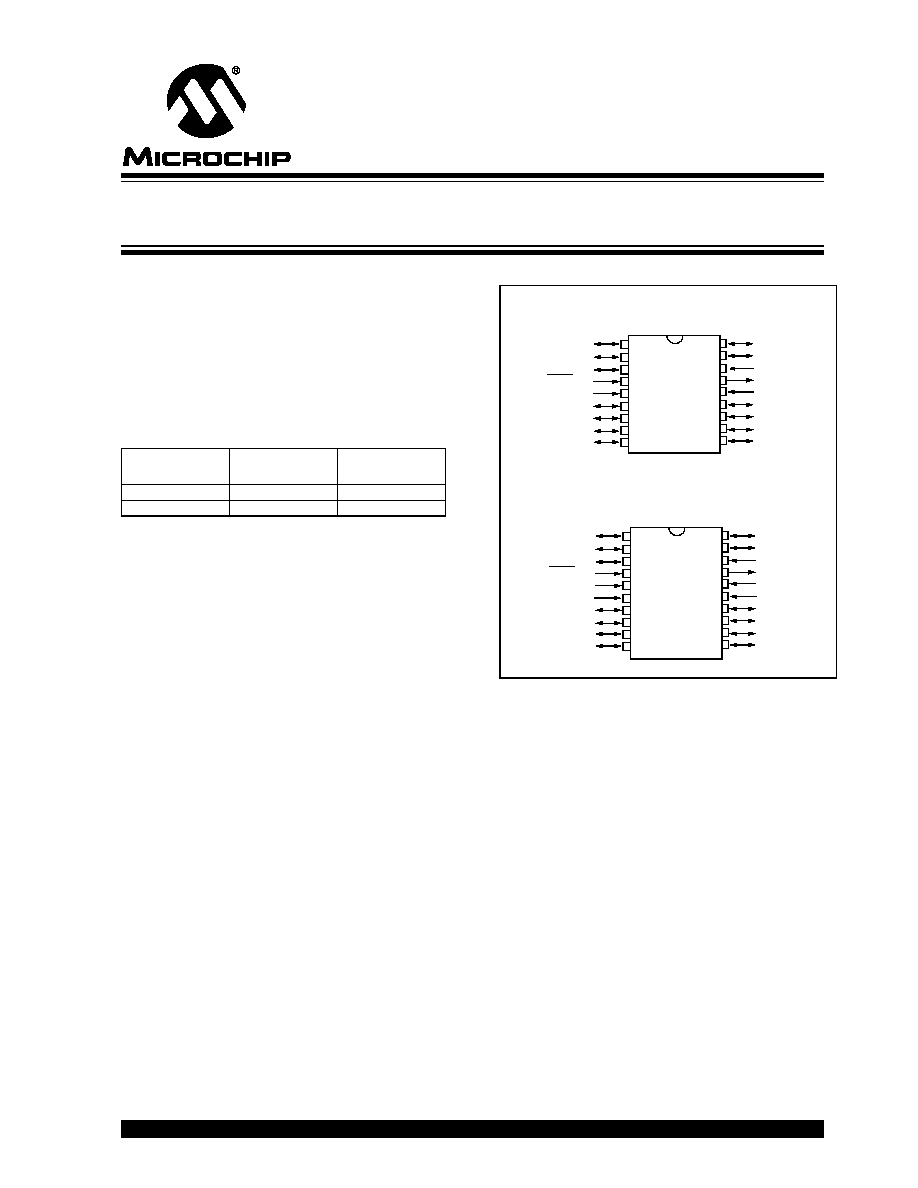
Pin Diagrams
Peripheral Features:
· Timer0: 8-bit timer/counter with 8-bit prescaler
· Timer1: 16-bit timer/counter with prescaler
can be incremented during sleep via external
crystal/clock
· Timer2: 8-bit timer/counter with 8-bit period
register, prescaler and postscaler
· Capture, Compare, PWM module
· Capture is 16-bit, max. resolution is 12.5 ns,
Compare is 16-bit, max. resolution is 200 ns,
PWM maximum resolution is 10-bit
· 8-bit multi-channel Analog-to-Digital converter
Device
Program
Memory
Data Memory
PIC16C712
1K
128
PIC16C716
2K
128
P
I
C16C
712
RA2/AN2
RA4/T0CKI
RB0/INT
RB1/T1OSO/T1CKI
RA0/AN0
OSC1/CLKIN
RB7
RB6
1
2
3
4
5
6
7
18
17
16
15
14
13
12
8
9
11
10
18-pin PDIP, SOIC, Windowed CERDIP
MCLR/V
PP
RA3/AN3/V
REF
RB2/T1OSI
RB3/CCP1
RB4
RB5
RA1/AN1
V
DD
OSC2/CLKOUT
V
SS
P
I
C16C
716
PI
C16C712
RA2/AN2
RA4/T0CKI
RB0/INT
RB1/T1OSO/T1CKI
RA0/AN0
OSC1/CLKIN
RB7
RB6
1
2
3
4
5
6
7
20
19
18
17
16
15
14
8
9
13
12
20-pin SSOP
MCLR/V
PP
RA3/AN3/V
REF
RB2/T1OSI
RB3/CCP1
RB4
RB5
RA1/AN1
V
DD
OSC2/CLKOUT
V
SS
PI
C16C716
10
V
SS
V
DD
11
PIC16C712/716
8-Bit CMOS Microcontrollers with A/D Converter
and Capture/Compare/PWM
PIC16C712/716
DS41106A-page 2
Preliminary
©
1999 Microchip Technology Inc.
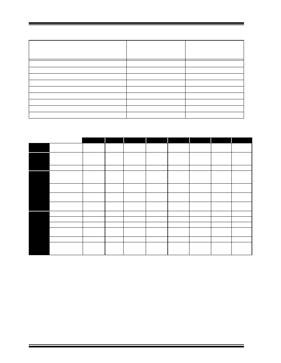
PIC16C7XX FAMILY OF DEVICES
Key Features
PICmicro
TM
Mid-Range Reference Manual
(DS33023)
PIC16C712
PIC16C716
Operating Frequency
DC - 20 MHz
DC - 20 MHz
Resets (and Delays)
POR, BOR (PWRT, OST)
POR, BOR (PWRT, OST)
Program Memory (14-bit words)
1K
2K
Data Memory (bytes)
128
128
Interrupts
7
7
I/O Ports
Ports A,B
Ports A,B
Timers
3
3
Capture/Compare/PWM modules
1
1
8-bit Analog-to-Digital Module
4 input channels
4 input channels
PIC16C710
PIC16C71
PIC16C711
PIC16C712
PIC16C715
PIC16C716
PIC16C72A
PIC16C73B
Clock
Maximum Frequency
of Operation (MHz)
20
20
20
20
20
20
20
20
Memory
EPROM Program
Memory
(x14 words)
512
1K
1K
1K
2K
2K
2K
4K
Data Memory (bytes)
36
36
68
128
128
128
128
192
Peripherals
Timer Module(s)
TMR0
TMR0
TMR0
TMR0
TMR1
TMR2
TMR0
TMR0
TMR1
TMR2
TMR0
TMR1
TMR2
TMR0
TMR1
TMR2
Capture/Compare/
PWM Module(s)
--
--
--
1
--
1
1
2
Serial Port(s)
(SPI/I
2
C, USART)
--
--
--
--
--
--
SPI/I
2
C
SPI/I
2
C,
USART
A/D Converter (8-bit)
Channels
4
4
4
4
4
4
5
5
Features
Interrupt Sources
4
4
4
7
4
7
8
11
I/O Pins
13
13
13
13
13
13
22
22
Voltage Range (Volts)
2.5-6.0
3.0-6.0
2.5-6.0
2.5-5.5
2.5-5.5
2.5-5.5
2.5-5.5
2.5-5.5
In-Circuit Serial
Programming
Yes
Yes
Yes
Yes
Yes
Yes
Yes
Yes
Brown-out Reset
Yes
--
Yes
Yes
Yes
Yes
Yes
Yes
Packages
18-pin DIP,
SOIC;
20-pin SSOP
18-pin DIP,
SOIC
18-pin DIP,
SOIC;
20-pin SSOP
18-pin DIP,
SOIC;
20-pin SSOP
18-pin DIP,
SOIC;
20-pin SSOP
18-pin DIP,
SOIC;
20-pin SSOP
28-pin SDIP,
SOIC, SSOP
28-pin SDIP,
SOIC

©
1999 Microchip Technology Inc.
Preliminary
DS41106A-page 3
PIC16C712/716
Table of Contents
1.0
Device Overview.................................................................................................................................................. 5
2.0
Memory Organization .......................................................................................................................................... 9
3.0
I/O Ports ............................................................................................................................................................ 21
4.0
Timer0 Module................................................................................................................................................... 29
5.0
Timer1 Module................................................................................................................................................... 31
6.0
Timer2 Module................................................................................................................................................... 36
7.0
Capture/Compare/PWM (CCP) Module(s) ........................................................................................................ 39
8.0
Analog-to-Digital Converter (A/D) Module ......................................................................................................... 45
9.0
Special Features of the CPU ............................................................................................................................. 51
10.0
Instruction Set Summary ................................................................................................................................... 67
11.0
Development Support........................................................................................................................................ 69
12.0
Electrical Characteristics ................................................................................................................................... 75
13.0
DC and AC Characteristics Graphs and Tables ................................................................................................ 91
14.0
Packaging Information....................................................................................................................................... 93
Revision History ........................................................................................................................................................... 99
Conversion Considerations .......................................................................................................................................... 99
Migration from Base-line to Mid-Range Devices .......................................................................................................... 99
Index ........................................................................................................................................................................... 101
On-Line Support.......................................................................................................................................................... 105
Reader Response ....................................................................................................................................................... 106
PIC16C712/716 Product Identification System ........................................................................................................... 107
To Our Valued Customers
Most Current Data Sheet
To obtain the most up-to-date version of this data sheet, please register at our Worldwide Web site at:
http://www.microchip.com
You can determine the version of a data sheet by examining its literature number found on the bottom outside corner of any page.
The last character of the literature number is the version number. e.g., DS30000A is version A of document DS30000.
New Customer Notification System
Register on our web site (www.microchip.com/cn) to receive the most current information on our products.
Errata
An errata sheet may exist for current devices, describing minor operational differences (from the data sheet) and recommended
workarounds. As device/documentation issues become known to us, we will publish an errata sheet. The errata will specify the revi-
sion of silicon and revision of document to which it applies.
To determine if an errata sheet exists for a particular device, please check with one of the following:
· Microchip's Worldwide Web site; http://www.microchip.com
· Your local Microchip sales office (see last page)
· The Microchip Corporate Literature Center; U.S. FAX: (480) 786-7277
When contacting a sales office or the literature center, please specify which device, revision of silicon and data sheet (include liter-
ature number) you are using.
Corrections to this Data Sheet
We constantly strive to improve the quality of all our products and documentation. We have spent a great deal of time to ensure
that this document is correct. However, we realize that we may have missed a few things. If you find any information that is missing
or appears in error, please:
· Fill out and mail in the reader response form in the back of this data sheet.
· E-mail us at webmaster@microchip.com.
We appreciate your assistance in making this a better document.
PIC16C712/716
©
1999 Microchip Technology Inc.
Preliminary
DS41106A-page 5
1.0
DEVICE OVERVIEW
This document contains device-specific information.
Additional information may be found in the PICmicroTM
Mid-Range Reference Manual, (DS33023), which may
be obtained from your local Microchip Sales Represen-
tative or downloaded from the Microchip website. The
Reference Manual should be considered a comple-
mentary document to this data sheet, and is highly rec-
ommended reading for a better understanding of the
device architecture and operation of the peripheral
modules.
There are two devices (PIC16C712, PIC16C716) cov-
ered by this datasheet.
Figure 1-1 is the block diagram for both devices. The
pinouts are listed in Table 1-1.
FIGURE 1-1:
PIC16C712/716 BLOCK DIAGRAM
EPROM
Program
Memory
13
Data Bus
8
14
Program
Bus
Instruction reg
Program Counter
8 Level Stack
(13-bit)
RAM
File
Registers
Direct Addr
7
RAM Addr
(1)
9
Addr MUX
Indirect
Addr
FSR reg
STATUS reg
MUX
ALU
W reg
Power-up
Timer
Oscillator
Start-up Timer
Power-on
Reset
Watchdog
Timer
Instruction
Decode &
Control
Timing
Generation
OSC1/CLKIN
OSC2/CLKOUT
MCLR
V
DD
, V
SS
PORTA
PORTB
RB0/INT
RB1/T1OSO/T1CKI
RB2/T1OSI
RB3/CCP1
RB4
RB5
RB6
RB7
8
8
Brown-out
Reset
Note 1:
Higher order bits are from the STATUS register.
CCP1
A/D
Timer0
Timer1
Timer2
RA4/T0CKI
RA3/AN3/V
REF
RA2/AN2
RA1/AN1
RA0/AN0
8
3
1K X 14
128 x 8
or
2K x 14