Äîêóìåíòàöèÿ è îïèñàíèÿ www.docs.chipfind.ru
©
1997 Microchip Technology Inc.
DS30444E - page 1
PIC16C9XX
8-Bit CMOS Microcontroller with LCD Driver
Devices included in this data sheet:
· PIC16C923
· PIC16C924
Microcontroller Core Features:
· High performance RISC CPU
· Only 35 single word instructions to learn
· 4K x 14 on-chip EPROM program memory
· 176 x 8 general purpose registers (SRAM)
· All single cycle instructions (500 ns) except for
program branches which are two-cycle
· Operating speed: DC - 8 MHz clock input
DC - 500 ns instruction cycle
· Interrupt capability
· Eight level deep hardware stack
· Direct, indirect and relative addressing modes
Peripheral Features:
· 25 I/O pins with individual direction control
· 25-27 input only pins
· Timer0: 8-bit timer/counter with 8-bit prescaler
· Timer1: 16-bit timer/counter, can be incremented
during sleep via external crystal/clock
· Timer2: 8-bit timer/counter with 8-bit period regis-
ter, prescaler and postscaler
· One pin that can be configured a capture input,
PWM output, or compare output
- Capture is 16-bit, max. resolution 31.25 ns
- Compare is 16-bit, max. resolution 500 ns
- PWM max resolution is 10-bits.
Maximum PWM frequency @ 8-bit resolution
= 32 kHz, @ 10-bit resolution = 8 kHz
· Programmable LCD timing module
- Multiple LCD timing sources available
- Can drive LCD panel while in Sleep mode
- Static, 1/2, 1/3, 1/4 multiplex
- Static drive and 1/3 bias capability
- 16 bytes of dedicated LCD RAM
- Up to 32 segments, up to 4 commons
Common
Segment
Pixels
1
32
32
2
31
62
3
30
90
4
29
116
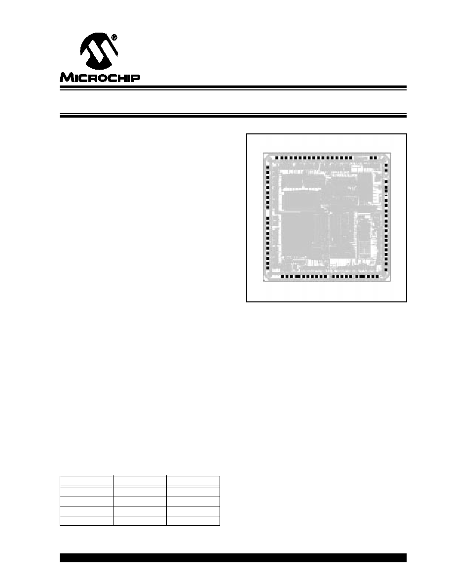
Available in Die Form
· Synchronous Serial Port (SSP) with SPI
TM
and I
2
C
TM
· 8-bit multi-channel Analog to Digital converter
(PIC16C924 only)
Special Microcontroller Features:
· Power-on Reset (POR)
· Power-up Timer (PWRT) and Oscillator Start-up
Timer (OST)
· Watchdog Timer (WDT) with its own on-chip RC
oscillator for reliable operation
· Programmable code-protection
· Power saving SLEEP mode
· Selectable oscillator options
· In-Circuit Serial ProgrammingTM (via two pins)
CMOS Technology
· Low-power, high-speed CMOS EPROM
technology
· Fully static design
· Wide operating voltage range: 2.5V to 6.0V
· Commercial and Industrial temperature ranges
· Low-power consumption:
- < 2 mA @ 5.5V, 4 MHz
- 22.5
µ
A typical @ 4V, 32 kHz
- < 1
µ
A typical standby current @ 3.0V
ICSP is a trademark of Microchip Technology Inc. I
2
C is a trademark of Philips Corporation. SPI is a trademark of Motorola Corporation.
PIC16C9XX
DS30444E - page 2
©
1997 Microchip Technology Inc.
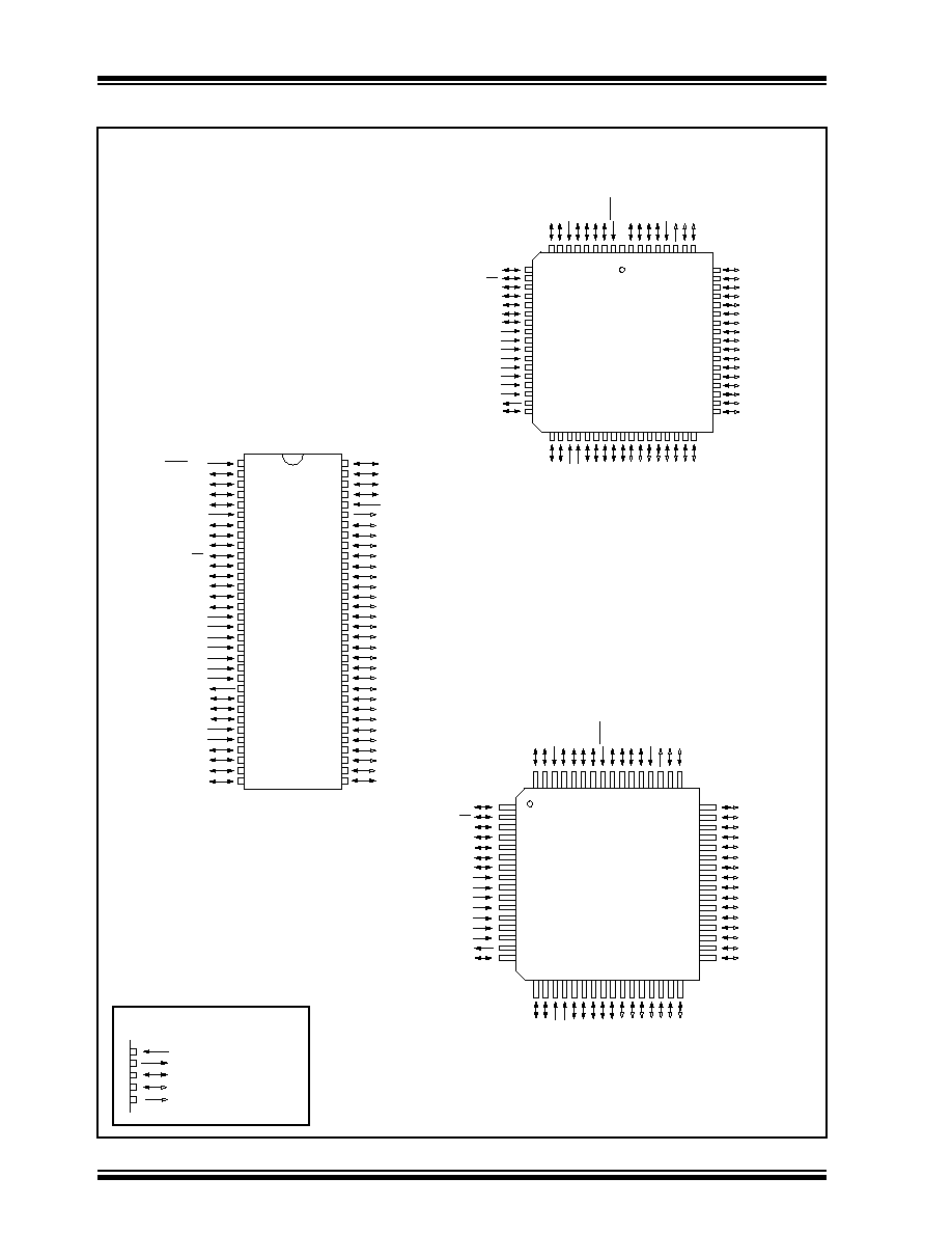
Pin Diagrams
TQFP
1
2
3
4
5
6
7
8
9
10
11
12
13
14
15
16
48
47
46
45
44
43
42
41
40
39
38
37
36
35
34
33
64
63
62
61
60
59
58
57
56
55
54
53
52
51
50
49
17
18
19
20
21
22
23
24
25
26
27
28
29
30
31
32
PIC16C923
RD5/SEG29/COM3
RG6/SEG26
RG3/SEG23
RG2/SEG22
RG1/SEG21
RG0/SEG20
RF7/SEG19
RF6/SEG18
RF5/SEG17
RF4/SEG16
RF3/SEG15
RF2/SEG14
RF1/SEG13
RF0/SEG12
RA4/T0CKI
RA5/SS
RB1
RB0/INT
RC3/SCK/SCL
RC4/SDI/SDA
RC5/SDO
V
LCD
2
V
LCD
3
V
DD
V
SS
C1
C2
OSC1/CLKIN
OSC2/CLKOUT
RC0/T1OSO/T1CKI
RA3
RA2
V
SS
RA1
RA0
RB2
RB3
RB4
RB5
RB7
RB6
V
DD
COM0
RD7/SEG31/COM1
RD6/SEG30/COM2
RC1/T1OSI
RC2/CCP1
V
LCD
1
VLCDADJ
RD0/SEG00
RD1/SEG01
RD2/SEG02
RD3/SEG03
RD4/SEG04
RE0/SEG05
RE1/SEG06
RE2/SEG07
RE3/SEG08
RE4/SEG09
RE6/SEG11
RE5/SEG10
RG5/SEG25
RG4/SEG24
MCLR
/
V
PP
10
11
12
13
14
15
16
17
18
19
20
21
22
23
24
25
26
60
59
58
57
56
55
54
53
52
51
50
49
48
47
46
45
44
9
8
7
6
5
4
3
2
1
68
67
66
65
64
63
62
61
27
28
29
30
31
32
33
34
35
36
37
38
39
40
41
42
43
PIC16C923
RD5/SEG29/COM3
RG6/SEG26
RG5/SEG25
RG4/SEG24
RG3/SEG23
RG2/SEG22
RG1/SEG21
RG0/SEG20
RG7/SEG28
RF7/SEG19
RF6/SEG18
RF5/SEG17
RF4/SEG16
RF3/SEG15
RF2/SEG14
RF1/SEG13
RF0/SEG12
RA4/T0CKI
RA5/SS
RB1
RB0/INT
RC3/SCK/SCL
RC4/SDI/SDA
RC5/SDO
V
LCD
2
V
LCD
3
V
DD
V
DD
V
SS
C1
C2
OSC1/CLKIN
OSC2/CLKOUT
RC0/T1OSO/T1CKI
RA3
RA2
V
SS
RA1
RA0
RB2
RB3
MCLR
/
V
PP
N/C
RB4
RB5
RB7
RB6
V
DD
COM0
RD7/SEG31/COM1
RD6/SEG30/COM2
RC1/T1OSI
RC2/CCP1
V
LCD
1
VLCDADJ
RD0/SEG00
RD1/SEG01
RD2/SEG02
RD3/SEG03
RD4/SEG04
RE7/SEG27
RE0/SEG05
RE1/SEG06
RE2/SEG07
RE3/SEG08
RE4/SEG09
RE6/SEG11
RE5/SEG10
PLCC
Input Pin
Output Pin
Digital Input/LCD Output Pin
LEGEND:
Input/Output Pin
LCD Output Pin
Shrink PDIP (750 mil)
RB4
RB5
RB7
RB6
V
DD
COM0
RD7/SEG31/COM1
RD6/SEG30/COM2
RD5/SEG29/COM3
RG6/SEG26
RG5/SEG25
RG4/SEG24
RG3/SEG23
RG2/SEG22
RG1/SEG21
RG0/SEG20
RF7/SEG19
RF6/SEG18
RF5/SEG17
RF4/SEG16
MCLR/V
PP
RB3
RB2
RA0
RA1
V
SS
RA2
RA4/T0CKI
RA5/SS
RB1
RB0/INT
RC3/SCK/SCL
RC4/SDI/SDA
RC5/SDO
V
LCD
2
V
LCD
3
V
DD
V
SS
C1
C2
1
2
3
4
5
6
7
8
9
10
11
12
13
14
15
16
17
18
19
20
64
63
62
61
60
59
58
57
56
55
54
53
52
51
50
49
48
47
46
45
PIC16C923
OSC1/CLKIN
OSC2/CLKOUT
RC0/T1OSO/T1CKI
RC1/T1OSI
RC2/CCP1
V
LCD
1
VLCDADJ
RD0/SEG00
RD1/SEG01
RD2/SEG02
RD3/SEG03
21
22
23
24
25
26
27
28
29
30
31
32
RA3
40
39
38
37
36
35
34
33
44
43
42
41
RF3/SEG15
RF2/SEG14
RF1/SEG13
RF0/SEG12
RE6/SEG11
RE5/SEG10
RE4/SEG09
RE3/SEG08
RE2/SEG07
RE1/SEG06
RE0/SEG05
RD4/SEG04
©
1997 Microchip Technology Inc.
DS30444E - page 3
PIC16C9XX
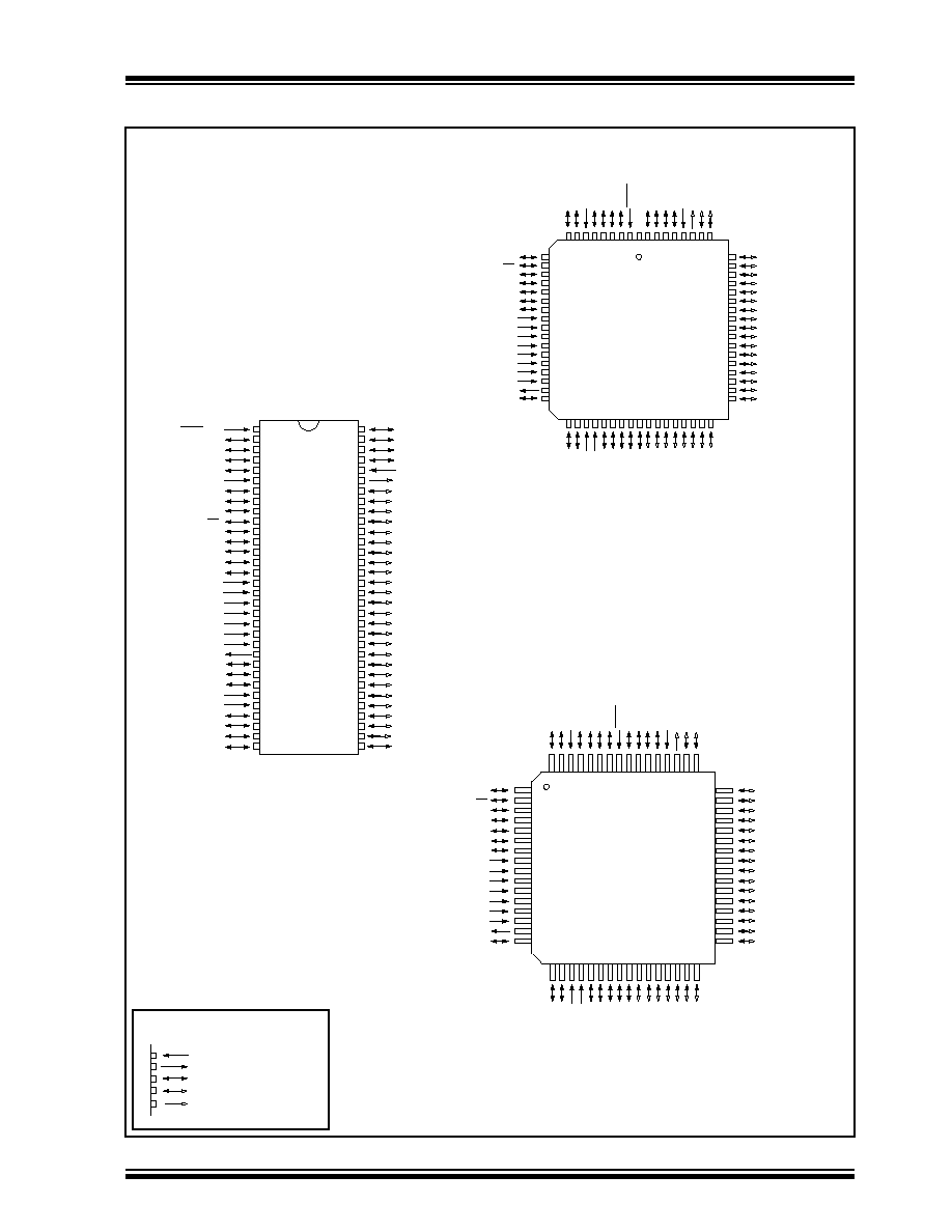
Pin Diagrams (Cont.'d)
10
11
12
13
14
15
16
17
18
19
20
21
22
23
24
25
26
60
59
58
57
56
55
54
53
52
51
50
49
48
47
46
45
44
9
8
7
6
5
4
3
2
1
68
67
66
65
64
63
62
61
27
28
29
30
31
32
33
34
35
36
37
38
39
40
41
42
43
PIC16C924
RD5/SEG29/COM3
RG6/SEG26
RG5/SEG25
RG4/SEG24
RG3/SEG23
RG2/SEG22
RG1/SEG21
RG0/SEG20
RG7/SEG28
RF7/SEG19
RF6/SEG18
RF5/SEG17
RF4/SEG16
RF3/SEG15
RF2/SEG14
RF1/SEG13
RF0/SEG12
RA4/T0CKI
RA5/AN4/SS
RB1
RB0/INT
RC3/SCK/SCL
RC4/SDI/SDA
RC5/SDO
V
LCD
2
V
LCD
3
A
VDD
V
DD
V
SS
C1
C2
OSC1/CLKIN
OSC2/CLKOUT
RC0/T1OSO/T1CKI
RA3/AN3/V
REF
RA2/AN2
V
SS
RA1/AN1
RA0/AN0
RB2
RB3
MCLR
/
V
PP
N/C
RB4
RB5
RB7
RB6
V
DD
COM0
RD7/SEG31/COM1
RD6/SEG30/COM2
RC1/T1OSI
RC2/CCP1
V
LCD
1
VLCDADJ
RD0/SEG00
RD1/SEG01
RD2/SEG02
RD3/SEG03
RD4/SEG04
RE7/SEG27
RE0/SEG05
RE1/SEG06
RE2/SEG07
RE3/SEG08
RE4/SEG09
RE6/SEG11
RE5/SEG10
PLCC
TQFP
1
2
3
4
5
6
7
8
9
10
11
12
13
14
15
16
48
47
46
45
44
43
42
41
40
39
38
37
36
35
34
33
64
63
62
61
60
59
58
57
56
55
54
53
52
51
50
49
17
18
19
20
21
22
23
24
25
26
27
28
29
30
31
32
PIC16C924
RD5/SEG29/COM3
RG6/SEG26
RG3/SEG23
RG2/SEG22
RG1/SEG21
RG0/SEG20
RF7/SEG19
RF6/SEG18
RF5/SEG17
RF4/SEG16
RF3/SEG15
RF2/SEG14
RF1/SEG13
RF0/SEG12
RA4/T0CKI
RA5/AN4/SS
RB1
RB0/INT
RC3/SCK/SCL
RC4/SDI/SDA
RC5/SDO
V
LCD
2
V
LCD
3
V
DD
V
SS
C1
C2
OSC1/CLKIN
OSC2/CLKOUT
RC0/T1OSO/T1CKI
RA3/AN3/
V
REF
RA2/AN2
V
SS
RA1/AN1
RA0/AN0
RB2
RB3
RB4
RB5
RB7
RB6
V
DD
COM0
RD7/SEG31/COM1
RD6/SEG30/COM2
RC1/T1OSI
RC2/CCP1
V
LCD
1
VLCDADJ
RD0/SEG00
RD1/SEG01
RD2/SEG02
RD3/SEG03
RD4/SEG04
RE0/SEG05
RE1/SEG06
RE2/SEG07
RE3/SEG08
RE4/SEG09
RE6/SEG11
RE5/SEG10
RG5/SEG25
RG4/SEG24
MCLR
/
V
PP
Input Pin
Output Pin
Digital Input/LCD Output Pin
LEGEND:
Input/Output Pin
LCD Output Pin
Shrink PDIP (750 mil)
RB4
RB5
RB7
RB6
V
DD
COM0
RD7/SEG31/COM1
RD6/SEG30/COM2
RD5/SEG29/COM3
RG6/SEG26
RG5/SEG25
RG4/SEG24
RG3/SEG23
RG2/SEG22
RG1/SEG21
RG0/SEG20
RF7/SEG19
RF6/SEG18
RF5/SEG17
RF4/SEG16
MCLR/V
PP
RB3
RB2
RA0/AN0
RA1/AN1
V
SS
RA2/AN2
RA4/T0CKI
RA5/AN4/SS
RB1
RB0/INT
RC3/SCK/SCL
RC4/SDI/SDA
RC5/SDO
V
LCD
2
V
LCD
3
V
DD
V
SS
C1
C2
1
2
3
4
5
6
7
8
9
10
11
12
13
14
15
16
17
18
19
20
64
63
62
61
60
59
58
57
56
55
54
53
52
51
50
49
48
47
46
45
PIC16C924
OSC1/CLKIN
OSC2/CLKOUT
RC0/T1OSO/T1CKI
RC1/T1OSI
RC2/CCP1
V
LCD
1
VLCDADJ
RD0/SEG00
RD1/SEG01
RD2/SEG02
RD3/SEG03
21
22
23
24
25
26
27
28
29
30
31
32
RA3/AN3/V
REF
40
39
38
37
36
35
34
33
44
43
42
41
RF3/SEG15
RF2/SEG14
RF1/SEG13
RF0/SEG12
RE6/SEG11
RE5/SEG10
RE4/SEG09
RE3/SEG08
RE2/SEG07
RE1/SEG06
RE0/SEG05
RD4/SEG04

PIC16C9XX
DS30444E - page 4
©
1997 Microchip Technology Inc.
Table of Contents
1.0
General Description..................................................................................................................................................................... 5
2.0
PIC16C9XX Device Varieties ...................................................................................................................................................... 7
3.0
Architectural Overview ................................................................................................................................................................ 9
4.0
Memory Organization ................................................................................................................................................................ 17
5.0
Ports .......................................................................................................................................................................................... 31
6.0
Overview of Timer Modules....................................................................................................................................................... 43
7.0
Timer0 Module .......................................................................................................................................................................... 45
8.0
Timer1 Module .......................................................................................................................................................................... 51
9.0
Timer2 Module .......................................................................................................................................................................... 55
10.0
Capture/Compare/PWM (CCP) Module .................................................................................................................................... 57
11.0
Synchronous Serial Port (SSP) Module .................................................................................................................................... 63
12.0
Analog-to-Digital Converter (A/D) Module ................................................................................................................................. 79
13.0
LCD Module .............................................................................................................................................................................. 89
14.0
Special Features of the CPU ................................................................................................................................................... 103
15.0
Instruction Set Summary ......................................................................................................................................................... 119
16.0
Development Support.............................................................................................................................................................. 137
17.0
Electrical Characteristics ......................................................................................................................................................... 141
18.0
DC and AC Characteristics Graphs and Tables ...................................................................................................................... 161
19.0
Packaging Information............................................................................................................................................................. 171
Appendix A:
................................................................................................................................................................................... 175
Appendix B:
Compatibility ............................................................................................................................................................. 175
Appendix C:
What's New................................................................................................................................................................ 176
Appendix D:
What's Changed ........................................................................................................................................................ 176
Index .................................................................................................................................................................................................. 177
List of Equations And Examples ........................................................................................................................................................ 181
List of Figures..................................................................................................................................................................................... 181
List of Tables...................................................................................................................................................................................... 182
Reader Response .............................................................................................................................................................................. 186
PIC16C9XX Product Identification System ........................................................................................................................................ 187
To Our Valued Customers
We constantly strive to improve the quality of all our products and documentation. We have spent an exceptional
amount of time to ensure that these documents are correct. However, we realize that we may have missed a few
things. If you find any information that is missing or appears in error, please use the reader response form in the
back of this data sheet to inform us. We appreciate your assistance in making this a better document.

©
1997 Microchip Technology Inc.
DS30444E- page 5
PIC16C9XX
1.0
GENERAL DESCRIPTION
The PIC16C9XX is a family of
low-cost, high-perfor-
mance, CMOS, fully-static, 8-bit microcontrollers with
an integrated LCD Driver module, in the PIC16CXXX
mid-range family.
All PICmicroTM microcontrollers employ an advanced
RISC architecture. The PIC16CXXX microcontroller
family has enhanced core features, eight-level deep
stack, and multiple internal and external interrupt
sources.
The separate instruction and data buses of the
Harvard architecture allow a 14-bit wide instruction
word with the separate 8-bit wide data. The two stage
instruction pipeline allows all instructions to execute in
a single cycle, except for program branches (which
require two cycles). A total of 35 instructions (reduced
instruction set) are available. Additionally, a large regis-
ter set gives some of the architectural innovations used
to achieve a very high performance.
PIC16CXXX microcontrollers typically achieve a 2:1
code compression and a 4:1 speed improvement over
other 8-bit microcontrollers in their class.
The
PIC16C923
devices have 176 bytes of RAM and
25 I/O pins. In addition several peripheral features are
available including: three timer/counters, one Cap-
ture/Compare/PWM module, one serial port and one
LCD module. The Synchronous Serial Port can be con-
figured as either a 3-wire Serial Peripheral Interface
(SPI) or the two-wire Inter-Integrated Circuit (I
2
C) bus.
The LCD module features programmable multiplex
mode (static, 1/2, 1/3 and 1/4) and drive bias (static and
1/3). It is capable of driving up to 32 segments and up
to 4 commons. It can also drive the LCD panel while in
SLEEP mode.
The
PIC16C924
devices have 176 bytes of RAM and
25 I/O pins. In addition several peripheral features are
available including: three timer/counters, one Cap-
ture/Compare/PWM module, one serial port and one
LCD module. The Synchronous Serial Port can be con-
figured as either a 3-wire Serial Peripheral Interface
(SPI) or the two-wire Inter-Integrated Circuit (I
2
C) bus.
The LCD module features programmable multiplex
mode (static, 1/2, 1/3 and 1/4) and drive bias (static and
1/3). It is capable of driving up to 32 segments and up
to 4 commons. It can also drive the LCD panel while in
SLEEP mode. The PIC16C924 also has an 5-channel
high-speed 8-bit A/D. The 8-bit resolution is ideally
suited for applications requiring low-cost analog inter-
face, e.g. thermostat control, pressure sensing, and
meters.
The PIC16C9XX family has special features to reduce
external components, thus reducing cost, enhancing
system reliability and reducing power consumption.
There are four oscillator options, of which the single pin
RC oscillator provides a low-cost solution, the LP oscil-
lator minimizes power consumption, XT is a standard
crystal, and the HS is for High Speed crystals. The
SLEEP (power-down) feature provides a power saving
mode. The user can wake up the chip from SLEEP
through several external and internal interrupts and
reset(s).
A highly reliable Watchdog Timer with its own on-chip
RC oscillator provides recovery in the event of a soft-
ware lock-up.
A UV erasable CERQUAD (compatible with PLCC)
packaged version is ideal for code development while
the cost-effective One-Time-Programmable (OTP) ver-
sion is suitable for production in any volume.
The PIC16C9XX family fits perfectly in applications
ranging from handheld meters, thermostats, to home
security products. The EPROM technology makes cus-
tomization of application programs (LCD panels, cali-
bration constants, sensor interfaces, etc.) extremely
fast and convenient. The small footprint packages make
this microcontroller series perfect for all applications
with space limitations. Low cost, low power, high perfor-
mance, ease of use and I/O flexibility make the
PIC16C9XX very versatile even in areas where no
microcontroller use has been considered before (e.g.
timer functions, capture and compare, PWM functions
and coprocessor applications).
1.1
Family and Upward Compatibility
Users familiar with the PIC16C5X microcontroller family
will realize that this is an enhanced version of the
PIC16C5X architecture. Please refer to Appendix A for
a detailed list of enhancements. Code written for the
PIC16C5X can be easily ported to the PIC16CXXX
family of devices (Appendix B).
1.2
Development Support
PIC16C9XX devices are supported by the complete
line of Microchip Development tools.
Please refer to Section 16.0 for more details about
Microchip's development tools.
PIC16C9XX
DS30444E - page 6
©
1997 Microchip Technology Inc.
TABLE 1-1: PIC16C9XX FAMILY OF DEVICES
PIC16C923
PIC16C924
Clock
Maximum Frequency of Operation (MHz)
8
8
Memory
EPROM Program Memory
4K
4K
Data Memory (bytes)
176
176
Peripherals
Timer Module(s)
TMR0,
TMR1,
TMR2
TMR0,
TMR1,
TMR2
Capture/Compare/PWM Module(s)
1
1
Serial Port(s)
(SPI/I
2
C, USART)
SPI/I
2
C
SPI/I
2
C
Parallel Slave Port
--
--
A/D Converter (8-bit) Channels
--
5
LCD Module
4 Com,
32 Seg
4 Com,
32 Seg
Features
Interrupt Sources
8
9
I/O Pins
25
25
Input Pins
27
27
Voltage Range (Volts)
2.5-6.0
2.5-6.0
In-Circuit Serial Programming
Yes
Yes
Brown-out Reset
--
--
Packages
64-pin SDIP,
TQFP;
68-pin PLCC,
Die
64-pin SDIP,
TQFP;
68-pin PLCC,
Die
All PICmicro Family devices have Power-on Reset, selectable Watchdog Timer, selectable code protect and high I/O current capabil-
ity. All PIC16C9XX Family devices use serial programming with clock pin RB6 and data pin RB7.

©
1997 Microchip Technology Inc.
DS30444E - page 7
PIC16C9XX
2.0
PIC16C9XX DEVICE VARIETIES
A variety of frequency ranges and packaging options
are available. Depending on application and production
requirements, the proper device option can be selected
using the information in the PIC16C9XX Product Iden-
tification System section at the end of this data sheet.
When placing orders, please use that page of the data
sheet to specify the correct part number.
For the PIC16C9XX family, there are two device "types"
as indicated in the device number:
1.
C
, as in PIC16
C
924. These devices have
EPROM type memory and operate over the
standard voltage range.
2.
LC
, as in PIC16
LC
924. These devices have
EPROM type memory and operate over an
extended voltage range.
2.1
UV Erasable Devices
The UV erasable version, offered in CERQUAD pack-
age, is optimal for prototype development and pilot pro-
grams.
The UV erasable version can be erased and repro-
grammed to any of the configuration modes.
Microchip's
PICSTART
®
Plus and PRO MATE
®
II pro-
grammers both support the PIC16C9XX. Third party
programmers also are available; refer to the
Microchip
Third Party Guide
for a list of sources.
2.2
One-Time-Programmable (OTP)
Devices
The availability of OTP devices is especially useful for
customers who need the flexibility for frequent code
updates and small volume applications.
The OTP devices, packaged in plastic packages, permit
the user to program them once. In addition to the pro-
gram memory, the configuration bits must also be pro-
grammed.
2.3
Quick-Turnaround-Production (QTP)
Devices
Microchip offers a QTP Programming Service for fac-
tory production orders. This service is made available
for users who choose not to program a medium to high
quantity of units and whose code patterns have stabi-
lized. The devices are identical to the OTP devices but
with all EPROM locations and configuration options
already programmed by the factory. Certain code and
prototype verification procedures apply before produc-
tion shipments are available. Please contact your local
Microchip Technology sales office for more details.
2.4
Serialized Quick-Turnaround
Production (SQTP
SM
) Devices
Microchip offers a unique programming service where
a few user-defined locations in each device are pro-
grammed with different serial numbers. The serial num-
bers may be random, pseudo-random or sequential.
Serial programming allows each device to have a
unique number which can serve as an entry-code,
password or ID number.

PIC16C9XX
DS30444E - page 8
©
1997 Microchip Technology Inc.
NOTES:

©
1997 Microchip Technology Inc.
DS30444E - page 9
PIC16C9XX
3.0
ARCHITECTURAL OVERVIEW
The high performance of the PIC16CXXX family can be
attributed to a number of architectural features com-
monly found in RISC microprocessors. To begin with,
the PIC16CXXX uses a Harvard architecture, in which,
program and data are accessed from separate memo-
ries using separate buses. This improves bandwidth
over traditional von Neumann architecture where pro-
gram and data are fetched from the same memory
using the same bus. Separating program and data
buses further allows instructions to be sized differently
than the 8-bit wide data word. Instruction opcodes are
14-bits wide making it possible to have all single word
instructions. A 14-bit wide program memory access bus
fetches a 14-bit instruction in a single cycle. A
two-stage pipeline overlaps fetch and execution of
instructions (Example 3-1). Consequently, all instruc-
tions execute in a single cycle (500 ns @ 8 MHz) except
for program branches.
The PIC16C923 and PIC16C924 both address 4K x 14
of program memory and 176 x 8 of data memory.
The PIC16CXXX can directly or indirectly address its
register files or data memory. All special function regis-
ters, including the program counter, are mapped in the
data memory. The PIC16CXXX has an orthogonal
(symmetrical) instruction set that makes it possible to
carry out any operation on any register using any
addressing mode. This symmetrical nature and lack of
`special optimal situations' make programming with the
PIC16CXXX simple yet efficient, thus significantly
reducing the learning curve.
PIC16CXXX devices contain an 8-bit ALU and working
register. The ALU is a general purpose arithmetic unit.
It performs arithmetic and Boolean functions between
the data in the working register and any register file.
The ALU is 8-bits wide and capable of addition, sub-
traction, shift and logical operations. Unless otherwise
mentioned, arithmetic operations are two's comple-
ment in nature. In two-operand instructions, typically
one operand is the working register (W register). The
other operand is a file register or an immediate con-
stant. In single operand instructions, the operand is
either the W register or a file register.
The W register is an 8-bit working register used for ALU
operations. It is not an addressable register.
Depending on the instruction executed, the ALU may
affect the values of the Carry (C), Digit Carry (DC), and
Zero (Z) bits in the STATUS register. The C and DC bits
operate as a borrow bit and a digit borrow out bit,
respectively, in subtraction. See the
SUBLW
and
SUBWF
instructions for examples.
PIC16C9XX
DS30444E - page 10
©
1997 Microchip Technology Inc.
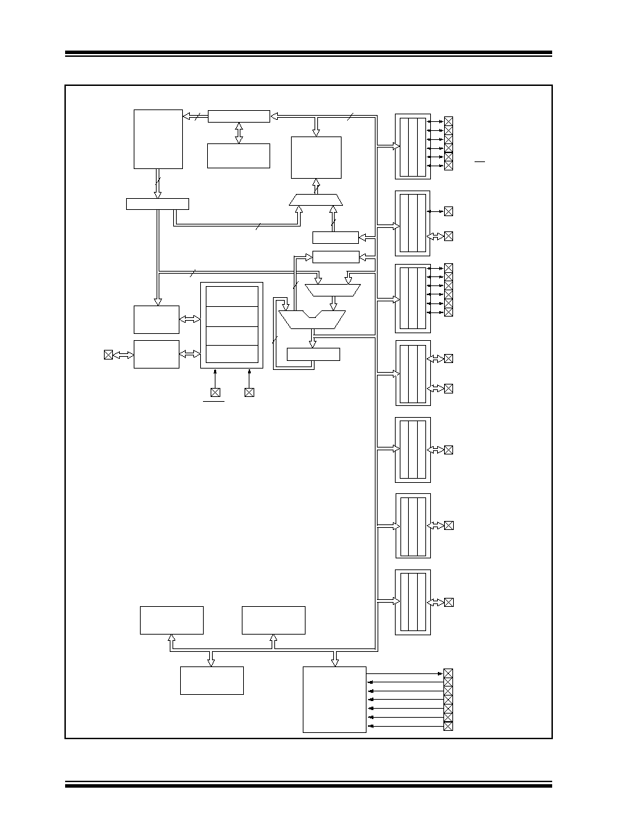
FIGURE 3-1:
PIC16C923 BLOCK DIAGRAM
EPROM
Program
Memory
4K x 14
13
Data Bus
8
14
Program
Bus
Instruction reg
Program Counter
8 Level Stack
(13-bit)
RAM
File
Registers
176 x 8
Direct Addr
7
RAM Addr
9
Addr MUX
Indirect
Addr
FSR reg
STATUS reg
MUX
ALU
W reg
Power-up
Timer
Oscillator
Start-up Timer
Power-on
Reset
Watchdog
Timer
Instruction
Decode &
Control
Timing
Generation
OSC1/CLKIN
OSC2/CLKOUT
MCLR
PORTA
PORTB
PORTC
PORTD
PORTE
RA4/T0CKI
RA5/SS
RB0/INT
RB1-RB7
RC0/T1OSO/T1CKI
RC1/T1OSI
RC2/CCP1
RC3/SCK/SCL
RC4/SDI/SDA
RC5/SDO
RD0-RD4/SEGnn
RE0-RE7/SEGnn
8
8
LCD
Synchronous
Timer0
Timer1, Timer2,
RA3
RA2
RA1
RA0
CCP1
Serial Port
V
LCD
1
PORTF
PORTG
RF0-RF7/SEGnn
RG0-RG7/SEGnn
RD5-RD7/SEGnn/COMn
COM0
3
8
V
DD
, V
SS
V
LCD
2
V
LCD
3
C1
C2
VLCDADJ
©
1997 Microchip Technology Inc.
DS30444E - page 11
PIC16C9XX
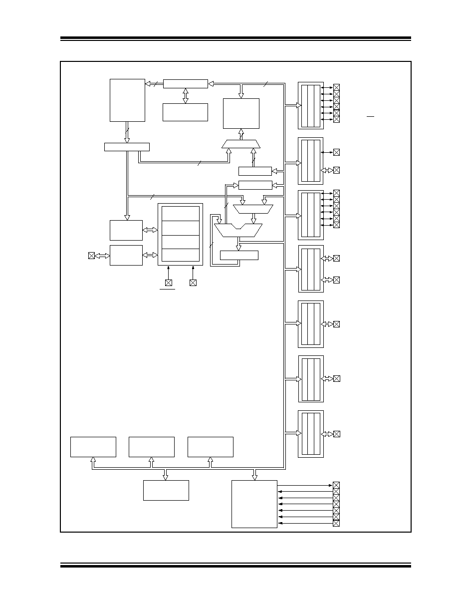
FIGURE 3-2:
PIC16C924 BLOCK DIAGRAM
EPROM
Program
Memory
4K x 14
13
Data Bus
8
14
Program
Bus
Instruction reg
Program Counter
8 Level Stack
(13-bit)
RAM
File
Registers
176 x 8
Direct Addr
7
RAM Addr
9
Addr MUX
Indirect
Addr
FSR reg
STATUS reg
MUX
ALU
W reg
Power-up
Timer
Oscillator
Start-up Timer
Power-on
Reset
Watchdog
Timer
Instruction
Decode &
Control
Timing
Generation
OSC1/CLKIN
OSC2/CLKOUT
MCLR
PORTA
PORTB
PORTC
PORTD
PORTE
RA4/T0CKI
RA5/AN4/SS
RB0/INT
RB1-RB7
RC0/T1OSO/T1CKI
RC1/T1OSI
RC2/CCP1
RC3/SCK/SCL
RC4/SDI/SDA
RC5/SDO
RD0-RD4/SEGnn
RE0-RE7/SEGnn
8
8
LCD
Synchronous
Timer0
Timer1, Timer2,
RA3/AN3/V
REF
RA2/AN2
RA1/AN1
RA0/AN0
CCP1
Serial Port
PORTF
PORTG
RF0-RF7/SEGnn
RG0-RG7/SEGnn
RD5-RD7/SEGnn/COMn
3
8
V
DD
, V
SS
A/D
V
LCD
1
COM0
V
LCD
2
V
LCD
3
C1
C2
VLCDADJ
PIC16C9XX
DS30444E - page 12
©
1997 Microchip Technology Inc.
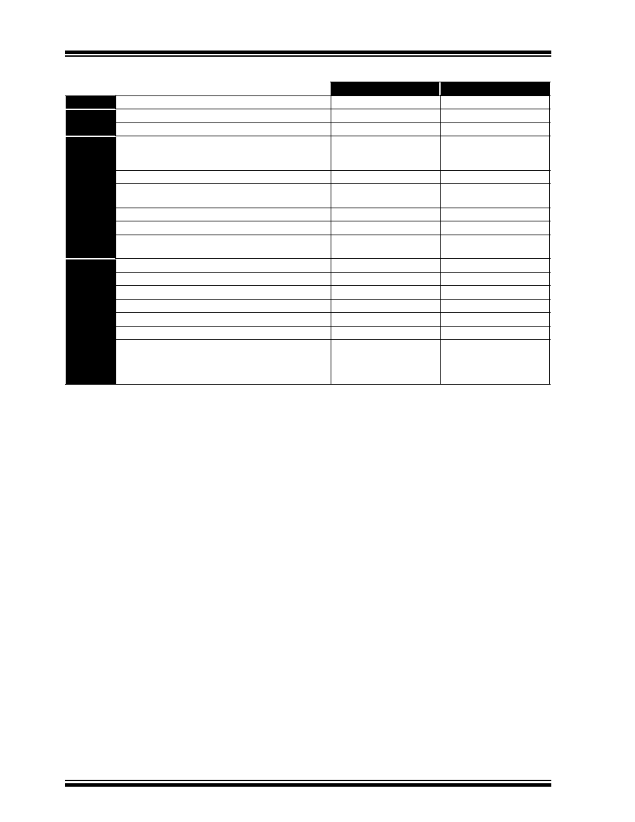
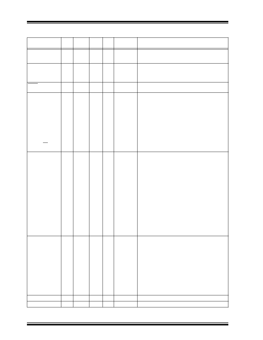
TABLE 3-1: PIC16C9XX PINOUT DESCRIPTION
Pin Name
DIP
Pin#
PLCC
Pin#
TQFP
Pin#
Pin
Type
Buffer
Type
Description
OSC1/CLKIN
22
24
14
I
ST/CMOS
Oscillator crystal input or external clock source input. This
buffer is a Schmitt Trigger input when configured in RC
oscillator mode and a CMOS input otherwise.
OSC2/CLKOUT
23
25
15
O
--
Oscillator crystal output. Connects to crystal or resonator
in crystal oscillator mode. In RC mode, OSC2 pin outputs
CLKOUT which has 1/4 the frequency of OSC1, and
denotes the instruction cycle rate.
MCLR/V
PP
1
2
57
I/P
ST
Master clear (reset) input or programming voltage input.
This pin is an active low reset to the device.
PORTA is a bi-directional I/O port. The AN and V
REF
multi-
plexed functions are used by the PIC16C924 only.
RA0/AN0
4
5
60
I/O
TTL
RA0 can also be Analog input0.
RA1/AN1
5
6
61
I/O
TTL
RA1 can also be Analog input1.
RA2/AN2
7
8
63
I/O
TTL
RA2 can also be Analog input2.
RA3/AN3/V
REF
8
9
64
I/O
TTL
RA3 can also be Analog input3 or A/D Voltage Refer-
ence.
RA4/T0CKI
9
10
1
I/O
ST
RA4 can also be the clock input to the Timer0
timer/counter. Output is open drain type.
RA5/AN4/SS
10
11
2
I/O
TTL
RA5 can be the slave select for the synchronous serial
port or Analog input4.
PORTB is a bi-directional I/O port. PORTB can be software
programmed for internal weak pull-ups on all inputs.
RB0/INT
12
13
4
I/O
TTL/ST
RB0 can also be the external interrupt pin. This buffer
is a Schmitt Trigger input when configured as an exter-
nal interrupt.
RB1
11
12
3
I/O
TTL
RB2
3
4
59
I/O
TTL
RB3
2
3
58
I/O
TTL
RB4
64
68
56
I/O
TTL
Interrupt on change pin.
RB5
63
67
55
I/O
TTL
Interrupt on change pin.
RB6
61
65
53
I/O
TTL/ST
Interrupt on change pin. Serial programming clock.
This buffer is a Schmitt Trigger input when used in
serial programming mode.
RB7
62
66
54
I/O
TTL/ST
Interrupt on change pin. Serial programming data.
This buffer is a Schmitt Trigger input when used in
serial programming mode.
PORTC is a bi-directional I/O port.
RC0/T1OSO/T1CKI
24
26
16
I/O
ST
RC0 can also be the Timer1 oscillator output or
Timer1 clock input.
RC1/T1OSI
25
27
17
I/O
ST
RC1 can also be the Timer1 oscillator input.
RC2/CCP1
26
28
18
I/O
ST
RC2 can also be the Capture1 input/Compare1 out-
put/PWM1 output.
RC3/SCK/SCL
13
14
5
I/O
ST
RC3 can also be the synchronous serial clock
input/output for both SPI and I
2
C modes.
RC4/SDI/SDA
14
15
6
I/O
ST
RC4 can also be the SPI Data In (SPI mode) or data
I/O (I
2
C mode).
RC5/SDO
15
16
7
I/O
ST
RC5 can also be the SPI Data Out (SPI mode).
C1
16
17
8
P
LCD Voltage Generation.
C2
17
18
9
P
LCD Voltage Generation.
Legend: I = input
O = output
P = power
L = LCD Driver
-- = Not used
TTL = TTL input
ST = Schmitt Trigger input
©
1997 Microchip Technology Inc.
DS30444E - page 13
PIC16C9XX
COM0
59
63
51
L
Common Driver0
PORTD is a digital input/output port. These pins are also
used as LCD Segment and/or Common Drivers.
RD0/SEG00
29
31
21
I/O/L
ST
Segment Driver00/Digital Input/Output.
RD1/SEG01
30
32
22
I/O/L
ST
Segment Driver01/Digital Input/Output.
RD2/SEG02
31
33
23
I/O/L
ST
Segment Driver02/Digital Input/Output.
RD3/SEG03
32
34
24
I/O/L
ST
Segment Driver03/Digital Input/Output.
RD4/SEG04
33
35
25
I/O/L
ST
Segment Driver04/Digital Input/Output.
RD5/SEG29/COM3
56
60
48
I/L
ST
Segment Driver29/Common Driver3/Digital Input.
RD6/SEG30/COM2
57
61
49
I/L
ST
Segment Driver30/Common Driver2/Digital Input.
RD7/SEG31/COM1
58
62
50
I/L
ST
Segment Driver31/Common Driver1/Digital Input.
PORTE is a digital input or LCD Segment Driver port.
RE0/SEG05
34
37
26
I/L
ST
Segment Driver05.
RE1/SEG06
35
38
27
I/L
ST
Segment Driver06.
RE2/SEG07
36
39
28
I/L
ST
Segment Driver07.
RE3/SEG08
37
40
29
I/L
ST
Segment Driver08.
RE4/SEG09
38
41
30
I/L
ST
Segment Driver09.
RE5/SEG10
39
42
31
I/L
ST
Segment Driver10.
RE6/SEG11
40
43
32
I/L
ST
Segment Driver11.
RE7/SEG27
-
36
-
I/L
ST
Segment Driver27 (Not available on 64-pin devices).
PORTF is a digital input or LCD Segment Driver port.
RF0/SEG12
41
44
33
I/L
ST
Segment Driver12.
RF1/SEG13
42
45
34
I/L
ST
Segment Driver13.
RF2/SEG14
43
46
35
I/L
ST
Segment Driver14.
RF3/SEG15
44
47
36
I/L
ST
Segment Driver15.
RF4/SEG16
45
48
37
I/L
ST
Segment Driver16.
RF5/SEG17
46
49
38
I/L
ST
Segment Driver17.
RF6/SEG18
47
50
39
I/L
ST
Segment Driver18.
RF7/SEG19
48
51
40
I/L
ST
Segment Driver19.
PORTG is a digital input or LCD Segment Driver port.
RG0/SEG20
49
53
41
I/L
ST
Segment Driver20.
RG1/SEG21
50
54
42
I/L
ST
Segment Driver21.
RG2/SEG22
51
55
43
I/L
ST
Segment Driver22.
RG3/SEG23
52
56
44
I/L
ST
Segment Driver23.
RG4/SEG24
53
57
45
I/L
ST
Segment Driver24.
RG5/SEG25
54
58
46
I/L
ST
Segment Driver25.
RG6/SEG26
55
59
47
I/L
ST
Segment Driver26.
RG7/SEG28
--
52
--
I/L
ST
Segment Driver28 (Not available on 64-pin devices).
VLCDADJ
28
30
20
P
LCD Voltage Generation.
A
VDD
--
21
--
P
Analog Power (PIC16C924 only).
V
DD
--
21
--
P
Power (PIC16C923 only).
V
LCD
1
27
29
19
P
LCD Voltage.
V
LCD
2
18
19
10
P
--
LCD Voltage.
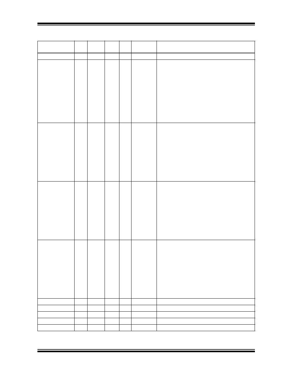
TABLE 3-1: PIC16C9XX PINOUT DESCRIPTION (Cont.'d)
Pin Name
DIP
Pin#
PLCC
Pin#
TQFP
Pin#
Pin
Type
Buffer
Type
Description
Legend: I = input
O = output
P = power
L = LCD Driver
-- = Not used
TTL = TTL input
ST = Schmitt Trigger input

PIC16C9XX
DS30444E - page 14
©
1997 Microchip Technology Inc.
V
LCD
3
19
20
11
P
--
LCD Voltage.
V
DD
20, 60
22, 64
12, 52
P
--
Digital power.
V
SS
6, 21
7, 23
13, 62
P
--
Ground reference.
NC
--
1
--
--
--
These pins are not internally connected. These pins should
be left unconnected.
TABLE 3-1: PIC16C9XX PINOUT DESCRIPTION (Cont.'d)
Pin Name
DIP
Pin#
PLCC
Pin#
TQFP
Pin#
Pin
Type
Buffer
Type
Description
Legend: I = input
O = output
P = power
L = LCD Driver
-- = Not used
TTL = TTL input
ST = Schmitt Trigger input
©
1997 Microchip Technology Inc.
DS30444E - page 15
PIC16C9XX
3.1
Clocking Scheme/Instruction Cycle
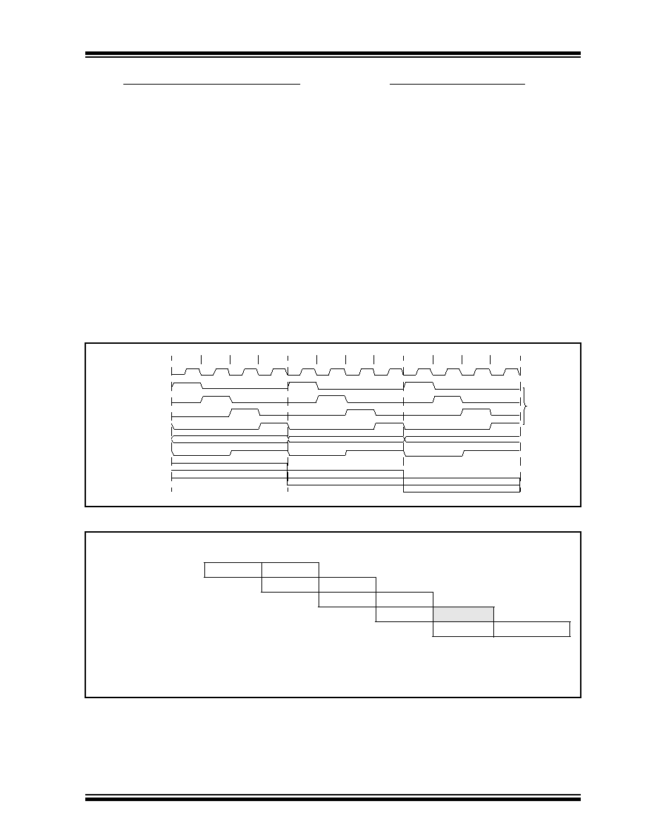
The clock input (from OSC1) is internally divided by
four to generate four non-overlapping quadrature
clocks namely Q1, Q2, Q3 and Q4. Internally, the pro-
gram counter (PC) is incremented every Q1, the
instruction is fetched from the program memory and
latched into the instruction register in Q4. The instruc-
tion is decoded and executed during the following Q1
through Q4. The clocks and instruction execution flow
is shown in Figure 3-3.
3.2
Instruction Flow/Pipelining
An "Instruction Cycle" consists of four Q cycles (Q1,
Q2, Q3 and Q4). The instruction fetch and execute are
pipelined such that fetch takes one instruction cycle
while decode and execute takes another instruction
cycle. However, due to the pipelining, each instruction
effectively executes in one cycle. If an instruction
causes the program counter to change (e.g.
GOTO
)
then two cycles are required to complete the instruction
(Example 3-1).
A fetch cycle begins with the program counter (PC)
incrementing in Q1.
In the execution cycle, the fetched instruction is latched
into the "Instruction Register" in cycle Q1. This instruc-
tion is then decoded and executed during the Q2, Q3,
and Q4 cycles. Data memory is read during Q2 (oper-
and read) and written during Q4 (destination write).
FIGURE 3-3:
CLOCK/INSTRUCTION CYCLE
EXAMPLE 3-1:
INSTRUCTION PIPELINE FLOW
Q1
Q2
Q3
Q4
Q1
Q2
Q3
Q4
Q1
Q2
Q3
Q4
OSC1
Q1
Q2
Q3
Q4
PC
OSC2/CLKOUT
(RC mode)
PC
PC+1
PC+2
Fetch INST (PC)
Execute INST (PC-1)
Fetch INST (PC+1)
Execute INST (PC)
Fetch INST (PC+2)
Execute INST (PC+1)
Internal
phase
clock
All instructions are single cycle, except for any program branches. These take two cycles since the fetch
instruction is "flushed" from the pipeline while the new instruction is being fetched and then executed.
Tcy0
Tcy1
Tcy2
Tcy3
Tcy4
Tcy5
1. MOVLW 55h
Fetch 1
Execute 1
2. MOVWF PORTB
Fetch 2
Execute 2
3. CALL SUB_1
Fetch 3
Execute 3
4. BSF PORTA, BIT3 (Forced NOP)
Fetch 4
Flush
5. Instruction @ address SUB_1
Fetch SUB_1 Execute SUB_1

PIC16C9XX
DS30444E - page 16
©
1997 Microchip Technology Inc.
NOTES:
©
1997 Microchip Technology Inc.
DS30444E - page 17
PIC16C9XX
4.0
MEMORY ORGANIZATION
4.1
Program Memory Organization
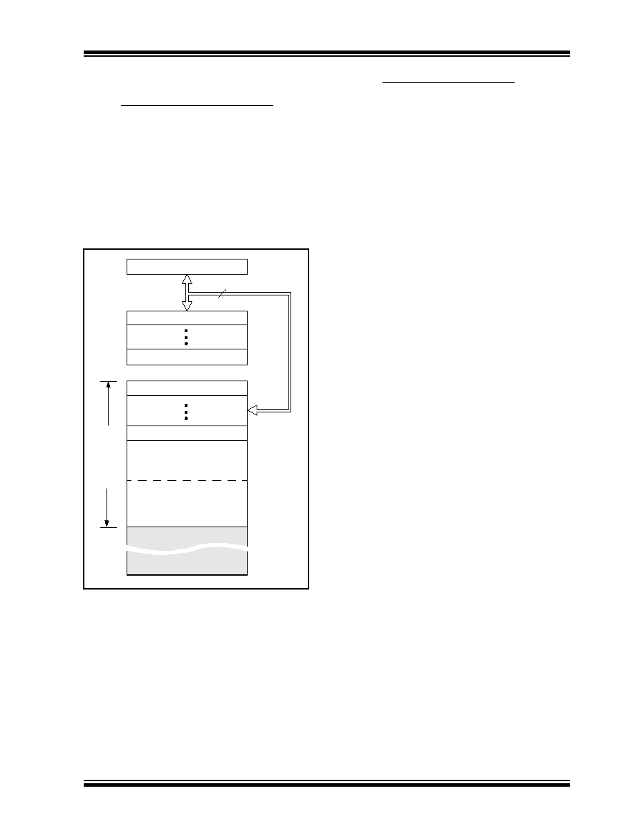
The PIC16C9XX family has a 13-bit program counter
capable of addressing an 8K x 14 program memory
space.
Only the first 4K x 14 (0000h-0FFFh) is physically
implemented. Accessing a location above the physi-
cally implemented addresses will cause a wraparound.
The reset vector is at 0000h and the interrupt vector is
at 0004h.
FIGURE 4-1:
PROGRAM MEMORY MAP
AND STACK
PC<12:0>
13
0000h
0004h
0005h
07FFh
0800h
0FFFh
1000h
1FFFh
Stack Level 1
Stack Level 8
Reset Vector
Interrupt Vector
On-chip Program
On-chip Program
Memory (Page 1)
Memory (Page 0)
CALL, RETURN
RETFIE, RETLW
User Memor
y
Space
4.2
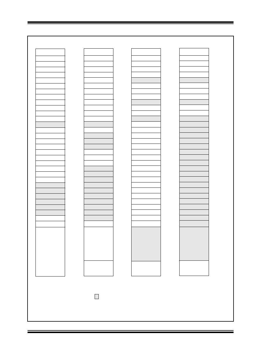
Data Memory Organization
The data memory is partitioned into four Banks which
contain the General Purpose Registers and the Special
Function Registers. Bits RP1 and RP0 are the bank
select bits.
RP1:RP0 (STATUS<6:5>)
11 = Bank 3 (180h-1FFh)
10 = Bank 2 (100h-17Fh)
01 = Bank 1 (80h-FFh)
00 = Bank 0 (00h-7Fh)
The lower locations of each Bank are reserved for the
Special Function Registers. Above the Special Func-
tion Registers are General Purpose Registers imple-
mented as static RAM. All four banks contain special
function registers. Some "high use" special function
registers are mirrored in other banks for code reduction
and quicker access.
4.2.1
GENERAL PURPOSE REGISTER FILE
The register file can be accessed either directly, or indi-
rectly through the File Select Register FSR
(Section
4.5).
The following General Purpose Registers are not phys-
ically implemented:
· F0h-FFh of Bank 1
· 170h-17Fh of Bank 2
· 1F0h-1FFh of Bank 3
These locations are used for common access across
banks.
PIC16C9XX
DS30444E - page 18
©
1997 Microchip Technology Inc.
FIGURE 4-2:
REGISTER FILE MAP
TRISF
TRISG
TRISB
PORTF
PORTG
PORTB
Indirect addr.
(1)
TMR0
PCL
STATUS
FSR
PORTA
PORTB
PORTC
PCLATH
INTCON
PIR1
TMR1L
TMR1H
T1CON
TMR2
T2CON
SSPBUF
SSPCON
CCPR1L
CCPR1H
CCP1CON
ADRES
(2)
ADCON0
(2)
OPTION
PCL
STATUS
FSR
TRISA
TRISB
TRISC
PCLATH
INTCON
PIE1
PCON
PR2
SSPADD
SSPSTAT
ADCON1
(2)
00h
01h
02h
03h
04h
05h
06h
07h
08h
09h
0Ah
0Bh
0Ch
0Dh
0Eh
0Fh
10h
11h
12h
13h
14h
15h
16h
17h
18h
19h
1Ah
1Bh
1Ch
1Dh
1Eh
1Fh
80h
81h
82h
83h
84h
85h
86h
87h
88h
89h
8Ah
8Bh
8Ch
8Dh
8Eh
8Fh
90h
91h
92h
93h
94h
95h
96h
97h
98h
99h
9Ah
9Bh
9Ch
9Dh
9Eh
9Fh
20h
A0h
General
Purpose
Register
General
Purpose
Register
7Fh
FFh
Bank 0
Bank 1
EFh
F0h
Unimplemented data memory locations, read as '0'.
Note
1: Not a physical register.
2: These registers are not implemented on the PIC16C923.
File
Address
Indirect addr.
(1)
Mapped in
70h-7Fh
Indirect addr.
(1)
PCL
STATUS
FSR
PCLATH
INTCON
PCL
STATUS
FSR
PCLATH
INTCON
LCDPS
LCDD02
LCDD03
LCDD04
LCDD15
100h
101h
102h
103h
104h
105h
106h
107h
108h
109h
10Ah
10Bh
10Ch
10Dh
10Eh
10Fh
110h
111h
112h
113h
114h
115h
116h
117h
118h
119h
11Ah
11Bh
11Ch
11Dh
11Eh
11Fh
180h
181h
182h
183h
184h
185h
186h
187h
188h
189h
18Ah
18Bh
18Ch
18Dh
18Eh
18Fh
190h
191h
192h
193h
194h
195h
196h
197h
198h
199h
19Ah
19Bh
19Ch
19Dh
19Eh
19Fh
120h
1A0h
17F
1FFh
Bank 2
Bank 3
1EFh
1F0h
Indirect addr.
(1)
16F
170
LCDD05
LCDD06
LCDD07
LCDD08
LCDD09
LCDD10
LCDD11
LCDD12
LCDD13
LCDD14
LCDCON
LCDD00
LCDD01
LCDSE
PORTD
PORTE
TRISD
TRISE
TMR0
OPTION
File
Address
File
Address
File
Address
Bank 0
Mapped in
70h-7Fh
Bank 0
Mapped in
70h-7Fh
Bank 0
©
1997 Microchip Technology Inc.
DS30444E - page 19
PIC16C9XX
4.2.2
SPECIAL FUNCTION REGISTERS
The Special Function Registers are registers used by
the CPU and Peripheral Modules for controlling the
desired operation of the device. These registers are
implemented as static RAM.
The special function registers can be classified into two
sets (core and peripheral). Those registers associated
with the "core" functions are described in this section,
and those related to the operation of the peripheral fea-
tures are described in the section of that peripheral fea-
ture.
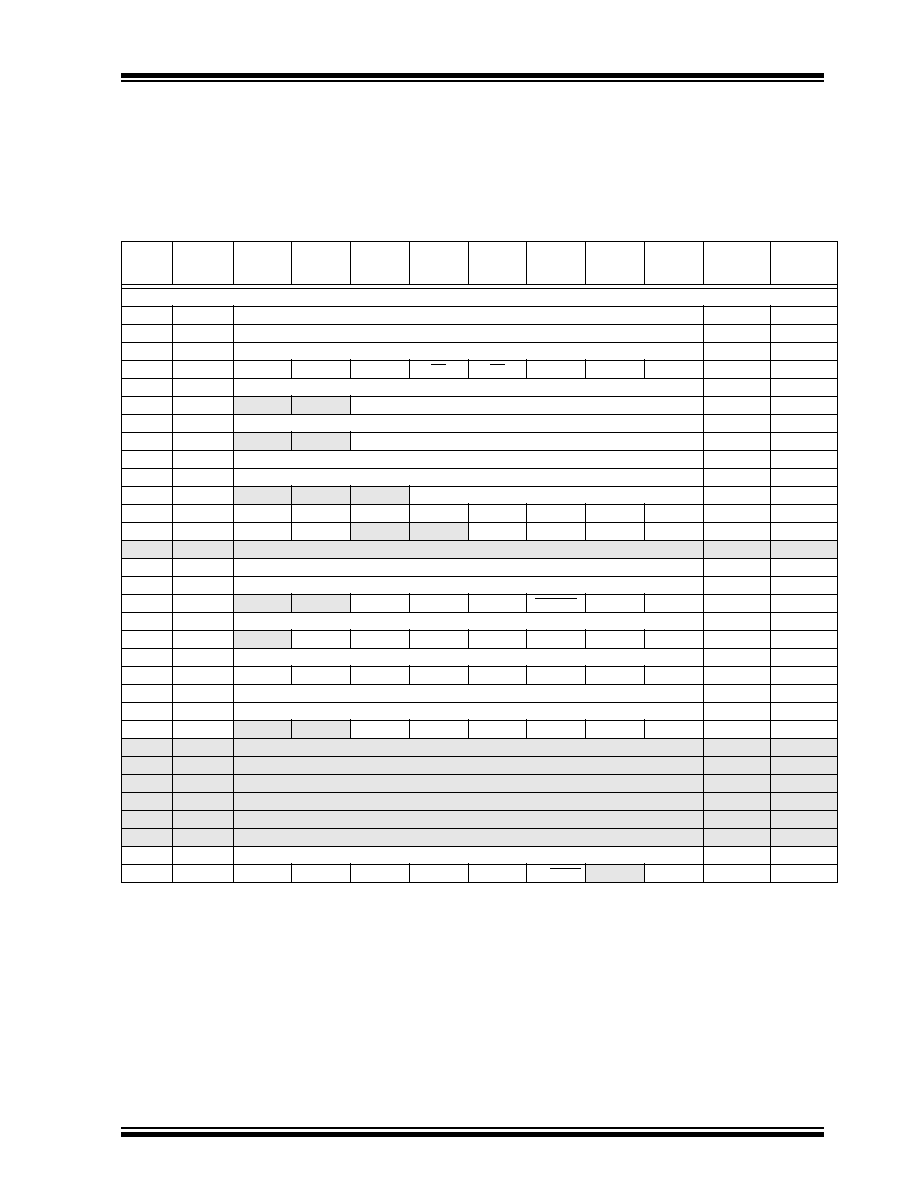
TABLE 4-1: SPECIAL FUNCTION REGISTER SUMMARY
Address Name
Bit 7
Bit 6
Bit 5
Bit 4
Bit 3
Bit 2
Bit 1
Bit 0
Value on
Power-on
Reset
Value on all
other resets
Bank 0
00h
INDF
Addressing this location uses contents of FSR to address data memory (not a physical register)
0000 0000
0000 0000
01h
TMR0
Timer0 module's register
xxxx xxxx
uuuu uuuu
02h
PCL
Program Counter's (PC) Least Significant Byte
0000 0000
0000 0000
03h
STATUS
IRP
RP1
RP0
TO
PD
Z
DC
C
0001 1xxx
000q quuu
04h
FSR
Indirect data memory address pointer
xxxx xxxx
uuuu uuuu
05h
PORTA
--
--
PORTA Data Latch when written: PORTA pins when read
(4)
(4)
06h
PORTB
PORTB Data Latch when written: PORTB pins when read
xxxx xxxx
uuuu uuuu
07h
PORTC
--
--
PORTC Data Latch when written: PORTC pins when read
--xx xxxx
--uu uuuu
08h
PORTD
PORTD Data Latch when written: PORTD pins when read
0000 0000
0000 0000
09h
PORTE
PORTE pins when read
0000 0000
0000 0000
0Ah
PCLATH
--
--
--
Write Buffer for the upper 5 bits of the Program Counter
---0 0000
---0 0000
0Bh
INTCON
GIE
PEIE
T0IE
INTE
RBIE
T0IF
INTF
RBIF
0000 000x
0000 000u
0Ch
PIR1
LCDIF
ADIF
(2)
--
--
SSPIF
CCP1IF
TMR2IF
TMR1IF
00-- 0000
00-- 0000
0Dh
--
Unimplemented
--
--
0Eh
TMR1L
Holding register for the Least Significant Byte of the 16-bit TMR1 register
xxxx xxxx
uuuu uuuu
0Fh
TMR1H
Holding register for the Most Significant Byte of the 16-bit TMR1 register
xxxx xxxx
uuuu uuuu
10h
T1CON
--
--
T1CKPS1
T1CKPS0
T1OSCEN
T1SYNC
TMR1CS
TMR1ON
--00 0000
--uu uuuu
11h
TMR2
Timer2 module's register
0000 0000
0000 0000
12h
T2CON
--
TOUTPS3
TOUTPS2
TOUTPS1
TOUTPS0
TMR2ON
T2CKPS1
T2CKPS0
-000 0000
-000 0000
13h
SSPBUF
Synchronous Serial Port Receive Buffer/Transmit Register
xxxx xxxx
uuuu uuuu
14h
SSPCON
WCOL
SSPOV
SSPEN
CKP
SSPM3
SSPM2
SSPM1
SSPM0
0000 0000
0000 0000
15h
CCPR1L
Capture/Compare/PWM Register (LSB)
xxxx xxxx
uuuu uuuu
16h
CCPR1H
Capture/Compare/PWM Register (MSB)
xxxx xxxx
uuuu uuuu
17h
CCP1CON
--
--
CCP1X
CCP1Y
CCP1M3
CCP1M2
CCP1M1
CCP1M0
--00 0000
--00 0000
18h
--
Unimplemented
--
--
19h
--
Unimplemented
--
--
1Ah
--
Unimplemented
--
--
1Bh
--
Unimplemented
--
--
1Ch
--
Unimplemented
--
--
1Dh
--
Unimplemented
--
--
1Eh
(1)
ADRES
A/D Result Register
xxxx xxxx
uuuu uuuu
1Fh
(1)
ADCON0
ADCS1
ADCS0
CHS2
CHS1
CHS0
GO/DONE
(5)
ADON
0000 0000
0000 0000
Legend:
x
= unknown,
u
= unchanged,
q
= value depends on condition, - = unimplemented read as '0',
shaded locations are unimplemented, read as `0'.
Note
1: Registers ADRES, ADCON0, and ADCON1 are not implemented in the PIC16C923, read as '0'.
2: These bits are reserved on the PIC16C923, always maintain these bits clear.
3: These pixels do not display, but can be used as general purpose RAM.
4: PIC16C923 reset values for PORTA:
--xx xxxx
for a POR, and
--uu uuuu
for all other resets,
PIC16C924 reset values for PORTA:
--0x 0000
when read.
5: Bit1 of ADCON0 is reserved on the PIC16C924, always maintain this bit clear.
PIC16C9XX
DS30444E - page 20
©
1997 Microchip Technology Inc.
Bank 1
80h
INDF
Addressing this location uses contents of FSR to address data memory (not a physical register)
0000 0000
0000 0000
81h
OPTION
RBPU
INTEDG
T0CS
T0SE
PSA
PS2
PS1
PS0
1111 1111
1111 1111
82h
PCL
Program Counter's (PC) Least Significant Byte
0000 0000
0000 0000
83h
STATUS
IRP
RP1
RP0
TO
PD
Z
DC
C
0001 1xxx
000q quuu
84h
FSR
Indirect data memory address pointer
xxxx xxxx
uuuu uuuu
85h
TRISA
--
--
PORTA Data Direction Register
--11 1111
--11 1111
86h
TRISB
PORTB Data Direction Register
1111 1111
1111 1111
87h
TRISC
--
--
PORTC Data Direction Register
--11 1111
--11 1111
88h
TRISD
PORTD Data Direction Register
1111 1111
1111 1111
89h
TRISE
PORTE Data Direction Register
1111 1111
1111 1111
8Ah
PCLATH
--
--
--
Write Buffer for the upper 5 bits of the PC
---0 0000
---0 0000
8Bh
INTCON
GIE
PEIE
T0IE
INTE
RBIE
T0IF
INTF
RBIF
0000 000x
0000 000u
8Ch
PIE1
LCDIE
ADIE
(2)
--
--
SSPIE
CCP1IE
TMR2IE
TMR1IE
00-- 0000
00-- 0000
8Dh
--
Unimplemented
--
--
8Eh
PCON
--
--
--
--
--
--
POR
--
---- --0-
---- --u-
8Fh
--
Unimplemented
--
--
90h
--
Unimplemented
--
--
91h
--
Unimplemented
--
--
92h
PR2
Timer2 Period Register
1111 1111
1111 1111
93h
SSPADD
Synchronous Serial Port (I
2
C mode) Address Register
0000 0000
0000 0000
94h
SSPSTAT
SMP
CKE
D/A
P
S
R/W
UA
BF
0000 0000
0000 0000
95h
--
Unimplemented
--
--
96h
--
Unimplemented
--
--
97h
--
Unimplemented
--
--
98h
--
Unimplemented
--
--
99h
--
Unimplemented
--
--
9Ah
--
Unimplemented
--
--
9Bh
--
Unimplemented
--
--
9Ch
--
Unimplemented
--
--
9Dh
--
Unimplemented
--
--
9Eh
--
Unimplemented
--
--
9Fh
(1)
ADCON1
--
--
--
--
--
PCFG2
PCFG1
PCFG0
---- -000 ---- -000
TABLE 4-1: SPECIAL FUNCTION REGISTER SUMMARY (Cont.'d)
Address Name
Bit 7
Bit 6
Bit 5
Bit 4
Bit 3
Bit 2
Bit 1
Bit 0
Value on
Power-on
Reset
Value on all
other resets
Legend:
x
= unknown,
u
= unchanged,
q
= value depends on condition, - = unimplemented read as '0',
shaded locations are unimplemented, read as `0'.
Note
1: Registers ADRES, ADCON0, and ADCON1 are not implemented in the PIC16C923, read as '0'.
2: These bits are reserved on the PIC16C923, always maintain these bits clear.
3: These pixels do not display, but can be used as general purpose RAM.
4: PIC16C923 reset values for PORTA:
--xx xxxx
for a POR, and
--uu uuuu
for all other resets,
PIC16C924 reset values for PORTA:
--0x 0000
when read.
5: Bit1 of ADCON0 is reserved on the PIC16C924, always maintain this bit clear.
©
1997 Microchip Technology Inc.
DS30444E - page 21
PIC16C9XX
Bank 2
100h
INDF
Addressing this location uses contents of FSR to address data memory (not a physical register)
0000 0000
0000 0000
101h
TMR0
Timer0 module's register
xxxx xxxx
uuuu uuuu
102h
PCL
Program Counter's (PC) Least Significant Byte
0000 0000
0000 0000
103h
STATUS
IRP
RP1
RP0
TO
PD
Z
DC
C
0001 1xxx
000q quuu
104h
FSR
Indirect data memory address pointer
xxxx xxxx
uuuu uuuu
105h
--
Unimplemented
--
--
106h
PORTB
PORTB Data Latch when written: PORTB pins when read
xxxx xxxx
uuuu uuuu
107h
PORTF
PORTF pins when read
0000 0000
0000 0000
108h
PORTG
PORTG pins when read
0000 0000
0000 0000
109h
--
Unimplemented
--
--
10Ah
PCLATH
--
--
--
Write Buffer for the upper 5 bits of the PC
---0 0000
---0 0000
10Bh
INTCON
GIE
PEIE
T0IE
INTE
RBIE
T0IF
INTF
RBIF
0000 000x
0000 000u
10Ch
--
Unimplemented
--
--
10Dh
LCDSE
SE29
SE27
SE20
SE16
SE12
SE9
SE5
SE0
1111 1111
1111 1111
10Eh
LCDPS
--
--
--
--
LP3
LP2
LP1
LP0
---- 0000
---- 0000
10Fh
LCDCON
LCDEN
SLPEN
--
VGEN
CS1
CS0
LMUX1
LMUX0
00-0 0000
00-0 0000
110h
LCDD00
SEG07
COM0
SEG06
COM0
SEG05
COM0
SEG04
COM0
SEG03
COM0
SEG02
COM0
SEG01
COM0
SEG00
COM0
xxxx xxxx
uuuu uuuu
111h
LCDD01
SEG15
COM0
SEG14
COM0
SEG13
COM0
SEG12
COM0
SEG11
COM0
SEG10
COM0
SEG09
COM0
SEG08
COM0
xxxx xxxx
uuuu uuuu
112h
LCDD02
SEG23
COM0
SEG22
COM0
SEG21
COM0
SEG20
COM0
SEG19
COM0
SEG18
COM0
SEG17
COM0
SEG16
COM0
xxxx xxxx
uuuu uuuu
113h
LCDD03
SEG31
COM0
SEG30
COM0
SEG29
COM0
SEG28
COM0
SEG27
COM0
SEG26
COM0
SEG25
COM0
SEG24
COM0
xxxx xxxx
uuuu uuuu
114h
LCDD04
SEG07
COM1
SEG06
COM1
SEG05
COM1
SEG04
COM1
SEG03
COM1
SEG02
COM1
SEG01
COM1
SEG00
COM1
xxxx xxxx
uuuu uuuu
115h
LCDD05
SEG15
COM1
SEG14
COM1
SEG13
COM1
SEG12
COM1
SEG11
COM1
SEG10
COM1
SEG09
COM1
SEG08
COM1
xxxx xxxx
uuuu uuuu
116h
LCDD06
SEG23
COM1
SEG22
COM1
SEG21
COM1
SEG20
COM1
SEG19
COM1
SEG18
COM1
SEG17
COM1
SEG16
COM1
xxxx xxxx
uuuu uuuu
117h
LCDD07
SEG31
COM1
(3)
SEG30
COM1
SEG29
COM1
SEG28
COM1
SEG27
COM1
SEG26
COM1
SEG25
COM1
SEG24
COM1
xxxx xxxx
uuuu uuuu
118h
LCDD08
SEG07
COM2
SEG06
COM2
SEG05
COM2
SEG04
COM2
SEG03
COM2
SEG02
COM2
SEG01
COM2
SEG00
COM2
xxxx xxxx
uuuu uuuu
119h
LCDD09
SEG15
COM2
SEG14
COM2
SEG13
COM2
SEG12
COM2
SEG11
COM2
SEG10
COM2
SEG09
COM2
SEG08
COM2
xxxx xxxx
uuuu uuuu
11Ah
LCDD10
SEG23
COM2
SEG22
COM2
SEG21
COM2
SEG20
COM2
SEG19
COM2
SEG18
COM2
SEG17
COM2
SEG16
COM2
xxxx xxxx
uuuu uuuu
11Bh
LCDD11
SEG31
COM2
(3)
SEG30
COM2
(3)
SEG29
COM2
SEG28
COM2
SEG27
COM2
SEG26
COM2
SEG25
COM2
SEG24
COM2
xxxx xxxx
uuuu uuuu
11Ch
LCDD12
SEG07
COM3
SEG06
COM3
SEG05
COM3
SEG04
COM3
SEG03
COM3
SEG02
COM3
SEG01
COM3
SEG00
COM3
xxxx xxxx
uuuu uuuu
11Dh
LCDD13
SEG15
COM3
SEG14
COM3
SEG13
COM3
SEG12
COM3
SEG11
COM3
SEG10
COM3
SEG09
COM3
SEG08
COM3
xxxx xxxx
uuuu uuuu
11Eh
LCDD14
SEG23
COM3
SEG22
COM3
SEG21
COM3
SEG20
COM3
SEG19
COM3
SEG18
COM3
SEG17
COM3
SEG16
COM3
xxxx xxxx
uuuu uuuu
11Fh
LCDD15
SEG31
COM3
(3)
SEG30
COM3
(3)
SEG29
COM3
(3)
SEG28
COM3
SEG27
COM3
SEG26
COM3
SEG25
COM3
SEG24
COM3
xxxx xxxx
uuuu uuuu
TABLE 4-1: SPECIAL FUNCTION REGISTER SUMMARY (Cont.'d)
Address Name
Bit 7
Bit 6
Bit 5
Bit 4
Bit 3
Bit 2
Bit 1
Bit 0
Value on
Power-on
Reset
Value on all
other resets
Legend:
x
= unknown,
u
= unchanged,
q
= value depends on condition, - = unimplemented read as '0',
shaded locations are unimplemented, read as `0'.
Note
1: Registers ADRES, ADCON0, and ADCON1 are not implemented in the PIC16C923, read as '0'.
2: These bits are reserved on the PIC16C923, always maintain these bits clear.
3: These pixels do not display, but can be used as general purpose RAM.
4: PIC16C923 reset values for PORTA:
--xx xxxx
for a POR, and
--uu uuuu
for all other resets,
PIC16C924 reset values for PORTA:
--0x 0000
when read.
5: Bit1 of ADCON0 is reserved on the PIC16C924, always maintain this bit clear.
PIC16C9XX
DS30444E - page 22
©
1997 Microchip Technology Inc.
Bank 3
180h
INDF
Addressing this location uses contents of FSR to address data memory (not a physical register)
0000 0000
0000 0000
181h
OPTION
RBPU
INTEDG
T0CS
T0SE
PSA
PS2
PS1
PS0
1111 1111
1111 1111
182h
PCL
Program Counter's (PC) Least Significant Byte
0000 0000
0000 0000
183h
STATUS
IRP
RP1
RP0
TO
PD
Z
DC
C
0001 1xxx
000q quuu
184h
FSR
Indirect data memory address pointer
xxxx xxxx
uuuu uuuu
185h
--
Unimplemented
--
--
186h
TRISB
PORTB Data Direction Register
1111 1111
1111 1111
187h
TRISF
PORTF Data Direction Register
1111 1111
1111 1111
188h
TRISG
PORTG Data Direction Register
1111 1111
1111 1111
189h
--
Unimplemented
--
--
18Ah
PCLATH
--
--
--
Write Buffer for the upper 5 bits of the PC
---0 0000
---0 0000
18Bh
INTCON
GIE
PEIE
T0IE
INTE
RBIE
T0IF
INTF
RBIF
0000 000x
0000 000u
18Ch
--
Unimplemented
--
--
18Dh
--
Unimplemented
--
--
18Eh
--
Unimplemented
--
--
18Fh
--
Unimplemented
--
--
190h
--
Unimplemented
--
--
191h
--
Unimplemented
--
--
192h
--
Unimplemented
--
--
193h
--
Unimplemented
--
--
194h
--
Unimplemented
--
--
195h
--
Unimplemented
--
--
196h
--
Unimplemented
--
--
197h
--
Unimplemented
--
--
198h
--
Unimplemented
--
--
199h
--
Unimplemented
--
--
19Ah
--
Unimplemented
--
--
19Bh
--
Unimplemented
--
--
19Ch
--
Unimplemented
--
--
19Dh
--
Unimplemented
--
--
19Eh
--
Unimplemented
--
--
19Fh
--
Unimplemented
--
--
TABLE 4-1: SPECIAL FUNCTION REGISTER SUMMARY (Cont.'d)
Address Name
Bit 7
Bit 6
Bit 5
Bit 4
Bit 3
Bit 2
Bit 1
Bit 0
Value on
Power-on
Reset
Value on all
other resets
Legend:
x
= unknown,
u
= unchanged,
q
= value depends on condition, - = unimplemented read as '0',
shaded locations are unimplemented, read as `0'.
Note
1: Registers ADRES, ADCON0, and ADCON1 are not implemented in the PIC16C923, read as '0'.
2: These bits are reserved on the PIC16C923, always maintain these bits clear.
3: These pixels do not display, but can be used as general purpose RAM.
4: PIC16C923 reset values for PORTA:
--xx xxxx
for a POR, and
--uu uuuu
for all other resets,
PIC16C924 reset values for PORTA:
--0x 0000
when read.
5: Bit1 of ADCON0 is reserved on the PIC16C924, always maintain this bit clear.
©
1997 Microchip Technology Inc.
DS30444E - page 23
PIC16C9XX
4.2.2.1
STATUS REGISTER
The STATUS register, shown in Figure 4-3, contains the
arithmetic status of the ALU, the RESET status and the
bank select bits for data memory.
The STATUS register can be the destination for any
instruction, as with any other register. If the STATUS
register is the destination for an instruction that affects
the Z, DC or C bits, then the write to these three bits is
disabled. These bits are set or cleared according to the
device logic. Furthermore, the TO and PD bits are not
writable. Therefore, the result of an instruction with the
STATUS register as destination may be different than
intended.
For example,
CLRF STATUS
will clear the upper-three
bits and set the Z bit. This leaves the STATUS register
as
000u u1uu
(where
u
= unchanged).
It is recommended, therefore, that only
BCF, BSF,
SWAPF
and
MOVWF
instructions are used to alter the
STATUS register because these instructions do not
affect the Z, C or DC bits from the STATUS register. For
other instructions, not affecting any status bits, see the
"Instruction Set Summary."
Note 1: The C and DC bits operate as a borrow
and digit borrow bit, respectively, in sub-
traction. See the
SUBLW
and
SUBWF
instructions for examples.
FIGURE 4-3:
STATUS REGISTER (ADDRESS 03h, 83h, 103h, 183h)
R/W-0
R/W-0
R/W-0
R-1
R-1
R/W-x
R/W-x
R/W-x
IRP
RP1
RP0
TO
PD
Z
DC
C
R = Readable bit
W = Writable bit
U = Unimplemented bit,
read as `0'
- n = Value at POR reset
bit7
bit0
bit 7:
IRP: Register Bank Select bit (used for indirect addressing)
1 = Bank 2, 3 (100h - 1FFh)
0 = Bank 0, 1 (00h - FFh)
bit 6-5: RP1:RP0: Register Bank Select bits (used for direct addressing)
11
= Bank 3 (180h - 1FFh)
10
= Bank 2 (100h - 17Fh)
01
= Bank 1 (80h - FFh)
00
= Bank 0 (00h - 7Fh)
bit 4:
TO: Time-out bit
1 = After power-up,
CLRWDT
instruction, or
SLEEP
instruction
0 = A WDT time-out occurred
bit 3:
PD: Power-down bit
1 = After power-up or by the
CLRWDT
instruction
0 = By execution of the
SLEEP
instruction
bit 2:
Z: Zero bit
1 = The result of an arithmetic or logic operation is zero
0 = The result of an arithmetic or logic operation is not zero
bit 1:
DC: Digit carry/borrow bit (
ADDWF
,
ADDLW,SUBLW,SUBWF
instructions) (for borrow the polarity is reversed)
1 = A carry-out from the 4th low order bit of the result occurred
0 = No carry-out from the 4th low order bit of the result
bit 0:
C: Carry/borrow bit (
ADDWF
,
ADDLW,SUBLW,SUBWF
instructions) (for borrow the polarity is reversed)
1 = A carry-out from the most significant bit of the result occurred
0 = No carry-out from the most significant bit of the result occurred
Note: A subtraction is executed by adding the two's complement of the second operand. For rotate (
RRF
,
RLF
) instructions, this bit is loaded with either the high or low order bit of the source register.

PIC16C9XX
DS30444E - page 24
©
1997 Microchip Technology Inc.
4.2.2.2
OPTION REGISTER
The OPTION register is a readable and writable regis-
ter which contains various control bits to configure the
TMR0/WDT prescaler, the external RB0/INT pin inter-
rupt, TMR0, and the weak pull-ups on PORTB.
Note:
To achieve a 1:1 prescaler assignment for
the TMR0 register, assign the prescaler to
the Watchdog Timer.
FIGURE 4-4:
OPTION REGISTER
(ADDRESS 81h, 181h)
R/W-1
R/W-1
R/W-1
R/W-1
R/W-1
R/W-1
R/W-1
R/W-1
RBPU
INTEDG
T0CS
T0SE
PSA
PS2
PS1
PS0
R
= Readable bit
W = Writable bit
U
= Unimplemented bit,
read as `0'
- n = Value at POR reset
bit7
bit0
bit 7:
RBPU: PORTB Pull-up Enable bit
1 = PORTB pull-ups are disabled
0 = PORTB pull-ups are enabled by individual port latch values
bit 6:
INTEDG: Interrupt Edge Select bit
1 = Interrupt on rising edge of RB0/INT pin
0 = Interrupt on falling edge of RB0/INT pin
bit 5:
T0CS: TMR0 Clock Source Select bit
1 = Transition on RA4/T0CKI pin
0 = Internal instruction cycle clock (CLKOUT)
bit 4:
T0SE: TMR0 Source Edge Select bit
1 = Increment on high-to-low transition on RA4/T0CKI pin
0 = Increment on low-to-high transition on RA4/T0CKI pin
bit 3:
PSA: Prescaler Assignment bit
1 = Prescaler is assigned to the WDT
0 = Prescaler is assigned to the Timer0 module
bit 2-0: PS2:PS0: Prescaler Rate Select bits
000
001
010
011
100
101
110
111
1 : 2
1 : 4
1 : 8
1 : 16
1 : 32
1 : 64
1 : 128
1 : 256
1 : 1
1 : 2
1 : 4
1 : 8
1 : 16
1 : 32
1 : 64
1 : 128
Bit Value
TMR0 Rate
WDT Rate
©
1997 Microchip Technology Inc.
DS30444E - page 25
PIC16C9XX
4.2.2.3
INTCON REGISTER
The INTCON Register is a readable and writable regis-
ter which contains various enable and flag bits for the
TMR0 register overflow, RB Port change and external
RB0/INT pin interrupts.
Note:
Interrupt flag bits get set when an interrupt
condition occurs regardless of the state of
its corresponding enable bit or the global
enable bit, GIE (INTCON<7>).
FIGURE 4-5:
INTCON REGISTER (ADDRESS 0Bh, 8Bh, 10Bh, 18Bh)
R/W-0
R/W-0
R/W-0
R/W-0
R/W-0
R/W-0
R/W-0
R/W-x
GIE
PEIE
T0IE
INTE
RBIE
T0IF
INTF
RBIF
R
= Readable bit
W = Writable bit
U
= Unimplemented bit,
read as `0'
- n = Value at POR reset
bit7
bit0
bit 7:
GIE: Global Interrupt Enable bit
1 = Enables all un-masked interrupts
0 = Disables all interrupts
bit 6:
PEIE: Peripheral Interrupt Enable bit
1 = Enables all un-masked peripheral interrupts
0 = Disables all peripheral interrupts
bit 5:
T0IE: TMR0 Overflow Interrupt Enable bit
1 = Enables the TMR0 interrupt
0 = Disables the TMR0 interrupt
bit 4:
INTE: RB0/INT External Interrupt Enable bit
1 = Enables the RB0/INT external interrupt
0 = Disables the RB0/INT external interrupt
bit 3:
RBIE: RB Port Change Interrupt Enable bit
1 = Enables the RB port change interrupt
0 = Disables the RB port change interrupt
bit 2:
T0IF: TMR0 Overflow Interrupt Flag bit
1 = TMR0 register has overflowed (must be cleared in software)
0 = TMR0 register did not overflow
bit 1:
INTF: RB0/INT External Interrupt Flag bit
1 = The RB0/INT external interrupt occurred (must be cleared in software)
0 = The RB0/INT external interrupt did not occur
bit 0:
RBIF: RB Port Change Interrupt Flag bit
1 = At least one of the RB7:RB4 pins changed state (see Section 5.2 to clear interrupt)
0 = None of the RB7:RB4 pins have changed state
Interrupt flag bits get set when an interrupt condition occurs regardless of the state of its corresponding enable bit or the
global enable bit, GIE (INTCON<7>). User software should ensure the appropriate interrupt flag bits are clear prior to
enabling an interrupt.
PIC16C9XX
DS30444E - page 26
©
1997 Microchip Technology Inc.
4.2.2.4
PIE1 REGISTER
This register contains the individual enable bits for the
peripheral interrupts.
Note:
Bit PEIE (INTCON<6>) must be set to
enable any peripheral interrupt.
FIGURE 4-6:
PIE1 REGISTER (ADDRESS 8Ch)
R/W-0
R/W-0
U-0
U-0
R/W-0
R/W-0
R/W-0
R/W-0
LCDIE
ADIE
(1)
--
--
SSPIE
CCP1IE
TMR2IE
TMR1IE
R
= Readable bit
W = Writable bit
U
= Unimplemented bit,
read as `0'
- n = Value at POR reset
bit7
bit0
bit 7:
LCDIE: LCD Interrupt Enable bit
1 = Enables the LCD interrupt
0 = Disables the LCD interrupt
bit 6:
ADIE: A/D Converter Interrupt Enable bit
(1)
1 = Enables the A/D interrupt
0 = Disables the A/D interrupt
bit 5-4: Unimplemented: Read as '0'
bit 3:
SSPIE: Synchronous Serial Port Interrupt Enable bit
1 = Enables the SSP interrupt
0 = Disables the SSP interrupt
bit 2:
CCP1IE: CCP1 Interrupt Enable bit
1 = Enables the CCP1 interrupt
0 = Disables the CCP1 interrupt
bit 1:
TMR2IE: TMR2 to PR2 Match Interrupt Enable bit
1 = Enables the TMR2 to PR2 match interrupt
0 = Disables the TMR2 to PR2 match interrupt
bit 0:
TMR1IE: TMR1 Overflow Interrupt Enable bit
1 = Enables the TMR1 overflow interrupt
0 = Disables the TMR1 overflow interrupt
Note 1: Bit ADIE is reserved on the PIC16C923, always maintain this bit clear.
©
1997 Microchip Technology Inc.
DS30444E - page 27
PIC16C9XX
4.2.2.5
PIR1 REGISTER
This register contains the individual flag bits for the
peripheral interrupts.
Note:
Interrupt flag bits get set when an interrupt
condition occurs regardless of the state of
its corresponding enable bit or the global
enable bit, GIE (INTCON<7>). User soft-
ware should ensure the appropriate inter-
rupt flag bits are clear prior to enabling an
interrupt.
FIGURE 4-7:
PIR1 REGISTER (ADDRESS 0Ch)
R/W-0
R/W-0
U-0
U-0
R/W-0
R/W-0
R/W-0
R/W-0
LCDIF
ADIF
(1)
--
--
SSPIF
CCP1IF
TMR2IF
TMR1IF
R
= Readable bit
W = Writable bit
U
= Unimplemented bit,
read as `0'
- n = Value at POR reset
bit7
bit0
bit 7:
LCDIF: LCD Interrupt Flag bit
1 = LCD interrupt occurred (must be cleared in software)
0 = LCD interrupt did not occur
bit 6:
ADIF: A/D Converter Interrupt Flag bit
(1)
1 = An A/D conversion completed (must be cleared in software)
0 = The A/D conversion is not complete
bit 5-4: Unimplemented: Read as '0'
bit 3:
SSPIF: Synchronous Serial Port Interrupt Flag bit
1 = The transmission/reception is complete (must be cleared in software)
0 = Waiting to transmit/receive
bit 2:
CCP1IF: CCP1 Interrupt Flag bit
Capture Mode
1 = A TMR1 register capture occurred (must be cleared in software)
0 = No TMR1 register capture occurred
Compare Mode
1 = A TMR1 register compare match occurred (must be cleared in software)
0 = No TMR1 register compare match occurred
PWM Mode
Unused in this mode
bit 1:
TMR2IF: TMR2 to PR2 Match Interrupt Flag bit
1 = TMR2 to PR2 match occurred (must be cleared in software)
0 = No TMR2 to PR2 match occurred
bit 0:
TMR1IF: TMR1 Overflow Interrupt Flag bit
1 = TMR1 register overflowed (must be cleared in software)
0 = TMR1 register did not overflow
Note 1: Bit ADIF is reserved on the PIC16C923, always maintain this bit clear.
Interrupt flag bits get set when an interrupt condition occurs regardless of the state of its corresponding enable bit or the
global enable bit, GIE (INTCON<7>). User software should ensure the appropriate interrupt flag bits are clear prior to
enabling an interrupt.
PIC16C9XX
DS30444E - page 28
©
1997 Microchip Technology Inc.
4.2.2.6
PCON REGISTER
The Power Control (PCON) register contains a flag bit
to allow differentiation between a Power-on Reset
(POR) to an external MCLR Reset or WDT Reset.
For various reset conditions see Table
14-4 and
Table
14-5.
FIGURE 4-8:
PCON REGISTER (ADDRESS 8Eh)
U-0
U-0
U-0
U-0
U-0
U-0
R/W-0
U-0
--
--
--
--
--
--
POR
--
R
= Readable bit
W = Writable bit
U
= Unimplemented bit,
read as `0'
- n = Value at POR reset
bit7
bit0
bit 7-2:
Unimplemented: Read as '0'
bit 1:
POR: Power-on Reset Status bit
1 = No Power-on Reset occurred
0 = A Power-on Reset occurred (must be set in software after a Power-on Reset occurs)
bit 0:
Unimplemented: Read as '0'
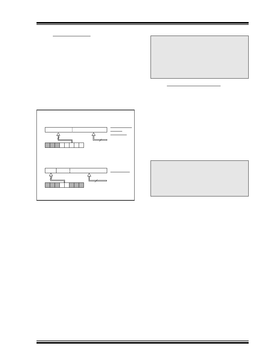
©
1997 Microchip Technology Inc.
DS30444E - page 29
PIC16C9XX
4.3
PCL and PCLATH
The program counter (PC) is 13-bits wide. The low byte
comes from the PCL register, which is a readable and
writable register. The upper bits (PC<12:8>) are not
readable, but are indirectly writable through the
PCLATH register. On any reset, the upper bits of the PC
will be cleared. Figure 4-9 shows the two situations for
the loading of the PC. The upper example in the figure
shows how the PC is loaded on a write to PCL
(PCLATH<4:0>
PCH). The lower example in the fig-
ure shows how the PC is loaded during a
CALL
or
GOTO
instruction (PCLATH<4:3>
PCH).
FIGURE 4-9:
LOADING OF PC IN
DIFFERENT SITUATIONS
4.3.1
COMPUTED GOTO
A computed GOTO is accomplished by adding an offset
to the program counter (
ADDWF PCL
). When doing a
table read using a computed GOTO method, care
should be exercised if the table location crosses a PCL
memory boundary (each 256 byte block). Refer to the
application note
"Implementing a Table Read" (AN556).
4.3.2
STACK
The PIC16CXXX family has an 8 level deep x 13-bit
wide hardware stack. The stack space is not part of
either program or data space and the stack pointer is
not readable or writable. The PC is PUSHed onto the
stack when a
CALL
instruction is executed or an inter-
rupt causes a branch. The stack is POPed in the event
of a
RETURN, RETLW
or a
RETFIE
instruction execu-
tion. PCLATH is not affected by a PUSH or POP oper-
ation.
The stack operates as a circular buffer. This means that
after the stack has been PUSHed eight times, the ninth
push overwrites the value that was stored from the first
push. The tenth push overwrites the second push (and
so on).
PC
12
8
7
0
5
PCLATH<4:0>
PCLATH
Instruction with
ALU result
GOTO, CALL
Opcode <10:0>
8
PC
12
11 10
0
11
PCLATH<4:3>
PCH
PCL
8
7
2
PCLATH
PCH
PCL
PCL as
Destination
4.4
Program Memory Paging
PIC16C9XX devices are capable of addressing a con-
tinuous 8K word block of program memory. The
CALL
and
GOTO
instructions provide only 11 bits of address
to allow branching within any 2K program memory
page. When doing a
CALL
or
GOTO
instruction the
upper 2 bits of the address are provided by
PCLATH<4:3>.
When doing a
CALL
or
GOTO
instruc-
tion, the user must ensure that the page select bits are
programmed so that the desired program memory
page is addressed. If a return from a
CALL
instruction
(or interrupt) is executed, the entire 13-bit PC is pushed
onto the stack. Therefore, manipulation of the
PCLATH<4:3> bits are not required for the return
instructions (which POPs the address from the stack).
Note 1: There are no status bits to indicate stack
overflow or stack underflow conditions.
Note 2: There are no instructions/mnemonics
called PUSH or POP. These are actions
that occur from the execution of the
CALL, RETURN, RETLW,
and
RETFIE
instructions, or the vectoring to an inter-
rupt address.
Note:
The PIC16C9XX ignores paging bit
PCLATH<4>, which is used to access pro-
gram memory pages 2 and 3. The use of
PCLATH<4> as a general purpose
read/write bit is not recommended since
this may affect upward compatibility with
future products.
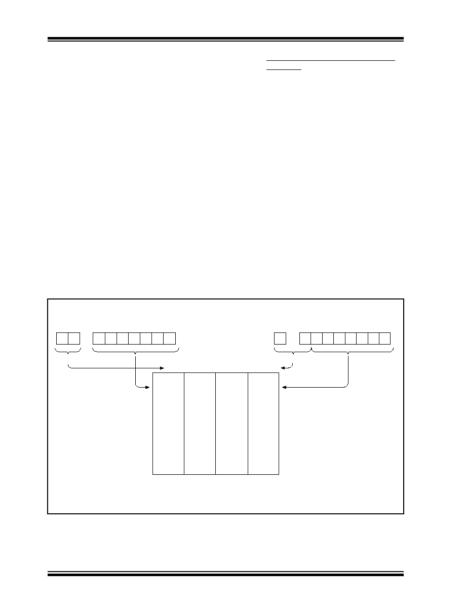
PIC16C9XX
DS30444E - page 30
©
1997 Microchip Technology Inc.
Example 4-1 shows the calling of a subroutine in
page 1 of the program memory. This example assumes
that PCLATH is saved and restored by the interrupt ser-
vice routine (if interrupts are used).
EXAMPLE 4-1:
CALL OF A SUBROUTINE IN
PAGE 1 FROM PAGE 0
ORG 0x500
BSF PCLATH,3 ;Select page 1 (800h-FFFh)
CALL SUB1_P1 ;Call subroutine in
: ;page 1 (800h-FFFh)
:
:
ORG 0x900
SUB1_P1: ;called subroutine
: ;page 1 (800h-FFFh)
:
RETURN ;return to Call subroutine
;in page 0 (000h-7FFh)
4.5
Indirect Addressing, INDF and FSR
Registers
The INDF register is not a physical register. Addressing
the INDF register will cause indirect addressing.
Indirect addressing is possible by using the INDF reg-
ister. Any instruction using the INDF register actually
accesses the register pointed to by the File Select Reg-
ister (FSR). Reading the INDF register itself indirectly
(FSR = '0') will produce 00h. Writing to the INDF regis-
ter indirectly results in a no-operation (although status
bits may be affected). An effective 9-bit address is
obtained by concatenating the 8-bit FSR register and
the IRP bit (STATUS<7>), as shown in Figure 4-10.
A simple program to clear RAM locations 20h-2Fh
using indirect addressing is shown in Example 4-2.
EXAMPLE 4-2:
INDIRECT ADDRESSING
movlw 0x20 ;initialize pointer
movwf FSR ;to RAM
NEXT clrf INDF ;clear INDF register
incf FSR,F ;inc pointer
btfss FSR,4 ;all done?
goto NEXT ;no clear next
CONTINUE
: ;yes continue
FIGURE 4-10: DIRECT/INDIRECT ADDRESSING
For memory map detail see Figure 4-2.
Data
Memory
Indirect Addressing
Direct Addressing
bank select
location select
RP1:RP0
6
0
from opcode
IRP
FSR register
7
0
bank select
location select
00
01
10
11
00h
7Fh
00h
7Fh
Bank 0
Bank 1
Bank 2
Bank 3
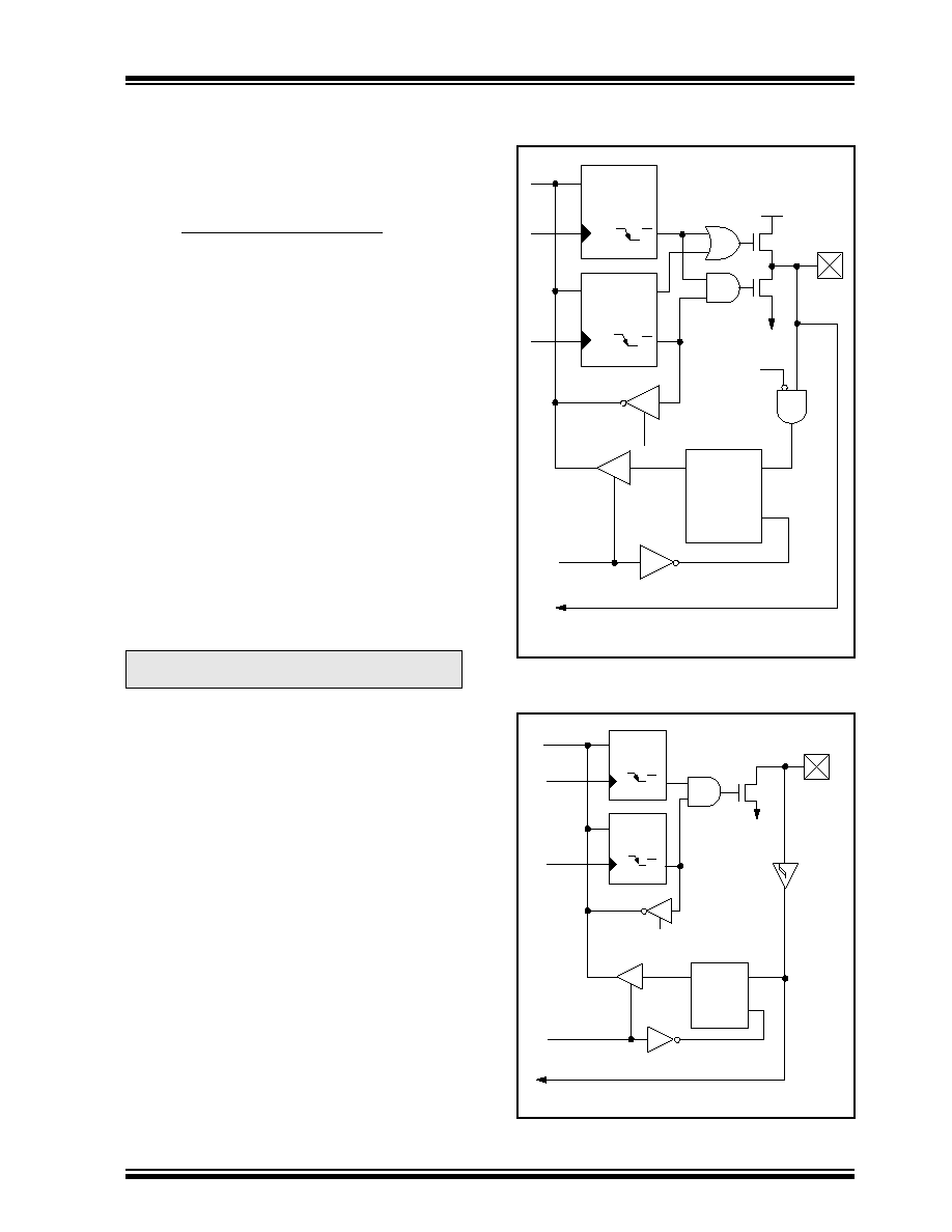
©
1997 Microchip Technology Inc.
DS30444E - page 31
PIC16C9XX
5.0
PORTS
Some pins for these ports are multiplexed with an alter-
nate function for the peripheral features on the device.
In general, when a peripheral is enabled, that pin may
not be used as a general purpose I/O pin.
5.1
PORTA and TRISA Register
The RA4/T0CKI pin is a Schmitt Trigger input and an
open drain output. All other RA port pins have TTL input
levels and full CMOS output drivers. All RA pins have
data direction bits (TRISA register) which can configure
these pins as output or input.
Setting a bit in the TRISA register puts the correspond-
ing output driver in a hi-impedance mode. Clearing a bit
in the TRISA register puts the contents of the output
latch on the selected pin.
Reading the PORTA register reads the status of the
pins whereas writing to it will write to the port latch. All
write operations are read-modify-write operations.
Therefore, a write to a port implies that the port pins are
read, this value is modified, and then written to the port
data latch.
Pin RA4 is multiplexed with the Timer0 module clock
input to become the RA4/T0CKI pin.
For the PIC16C924 only, other PORTA pins are multi-
plexed with analog inputs and the analog V
REF
input.
The operation of each pin is selected by clearing/set-
ting the control bits in the ADCON1 register (A/D Con-
trol Register1).
The TRISA register controls the direction of the RA
pins, even when they are being used as analog inputs.
The user must ensure the bits in the TRISA register are
maintained set when using them as analog inputs.
EXAMPLE 5-1:
INITIALIZING PORTA
BCF STATUS, RP0 ; Select Bank0
BCF STATUS, RP1
CLRF PORTA ; Initialize PORTA
BSF STATUS, RP0 ;
MOVLW 0xCF ; Value used to
; initialize data
; direction
MOVWF TRISA ; Set RA<3:0> as inputs
; RA<5:4> as outputs
; RA<7:6> are always
; read as '0'.
Note:
On a Power-on Reset, these pins are con-
figured as analog inputs and read as '0'.
FIGURE 5-1:
BLOCK DIAGRAM OF PINS
RA3:RA0 AND RA5
FIGURE 5-2:
BLOCK DIAGRAM OF
RA4/T0CKI PIN
Data
bus
Q
D
Q
CK
Q
D
Q
CK
Q
D
EN
P
N
WR
Port
WR
TRIS
Data Latch
TRIS Latch
RD TRIS
RD PORT
V
SS
V
DD
I/O pin
(1)
Note 1: I/O pins have protection diodes to V
DD
and V
SS
.
Analog
input
mode
TTL
input
buffer
To A/D Converter (PIC16C924 only)
Data
bus
WR
PORT
WR
TRIS
RD PORT
Data Latch
TRIS Latch
RD TRIS
Schmitt
Trigger
input
buffer
N
V
SS
I/O pin
(1)
TMR0 clock input
Note 1: I/O pin has protection diodes to V
SS
only.
Q
D
Q
CK
Q
D
Q
CK
EN
Q
D
EN
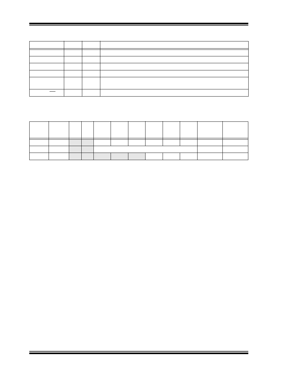
PIC16C9XX
DS30444E - page 32
©
1997 Microchip Technology Inc.
TABLE 5-1: PORTA FUNCTIONS
TABLE 5-2: SUMMARY OF REGISTERS ASSOCIATED WITH PORTA
Name
Bit#
Buffer
Function
RA0/AN0
(1)
bit0
TTL
Input/output or analog input
RA1/AN1
(1)
bit1
TTL
Input/output or analog input
RA2/AN2
(1)
bit2
TTL
Input/output or analog input
RA3/AN3/V
REF
(1)
bit3
TTL
Input/output or analog input or V
REF
RA4/T0CKI
bit4
ST
Input/output or external clock input for Timer0
Output is open drain type
RA5/AN4/SS
(1)
bit5
TTL
Input/output or analog input or slave select input for synchronous serial port
Legend: TTL = TTL input, ST = Schmitt Trigger input
Note 1: The AN and V
REF
functions are for the A/D module and are only implemented on the PIC16C924.
Address
Name
Bit 7
Bit 6
Bit 5
Bit 4
Bit 3
Bit 2
Bit 1
Bit 0
Value on
Power-on
Reset
Value on
all other
resets
05h
PORTA
--
--
RA5
RA4
RA3
RA2
RA1
RA0
(2)
(2)
85h
TRISA
--
--
PORTA Data Direction Control Register
--11 1111
--11 1111
9Fh
(1)
ADCON1
--
--
--
--
--
PCFG2
PCFG1
PCFG0
---- -000
---- -000
Legend:
x
= unknown,
u
= unchanged,
-
= unimplemented locations read as '0'. Shaded cells are not used by PORTA.
Note
1: The ADCON1 register is implemented on the PIC16C924 only.
2: PIC16C923 reset values for PORTA:
--xx xxxx
for a POR, and
--uu uuuu
for all other resets,
PIC16C924 reset values for PORTA:
--0x 0000
when read.
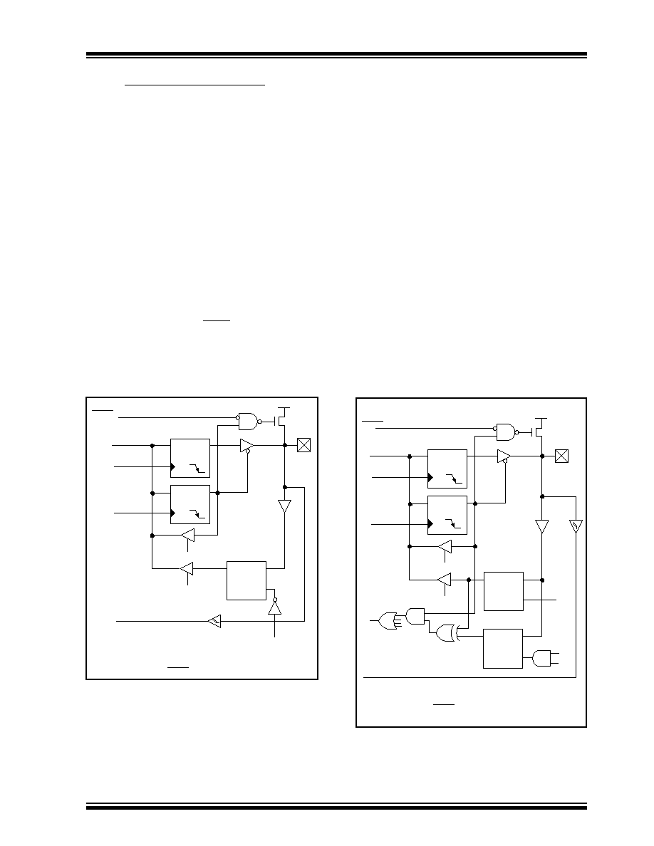
©
1997 Microchip Technology Inc.
DS30444E - page 33
PIC16C9XX
5.2
PORTB and TRISB Register
PORTB is an 8-bit wide bi-directional port. The corre-
sponding data direction register is TRISB. Setting a bit
in the TRISB register puts the corresponding output
driver in a hi-impedance input mode. Clearing a bit in
the TRISB register puts the contents of the output latch
on the selected pin(s).
EXAMPLE 5-2:
INITIALIZING PORTB
BCF STATUS, RP0 ; Select Bank0
BCF STATUS, RP1
CLRF PORTB ; Initialize PORTB
BSF STATUS, RP0 ;
MOVLW 0xCF ; Value used to
; initialize data
; direction
MOVWF TRISB ; Set RB<3:0> as inputs
; RB<5:4> as outputs
; RB<7:6> as inputs
Each of the PORTB pins has a weak internal pull-up. A
single control bit can turn on all the pull-ups. This is
performed by clearing bit RBPU (OPTION<7>). The
weak pull-up is automatically turned off when the port
pin is configured as an output. The pull-ups are also dis-
abled on a Power-on Reset.
FIGURE 5-3:
BLOCK DIAGRAM OF
RB3:RB0 PINS
Four of PORTB's pins, RB7:RB4, have an interrupt on
change feature. Only pins configured as inputs can
cause this interrupt to occur (i.e. any RB7:RB4 pin con-
figured as an output is excluded from the interrupt on
change comparison). The input pins (of RB7:RB4) are
compared with the old value latched on the last read of
Data Latch
RBPU
(2)
P
V
DD
Q
D
CK
Q
D
CK
Q
D
EN
Data bus
WR Port
WR TRIS
RD TRIS
RD Port
weak
pull-up
RD Port
RB0/INT
I/O
pin
(1)
TTL
Input
Buffer
Note 1: I/O pins have diode protection to V
DD
and V
SS
.
2: To enable weak pull-ups, set the appropriate TRIS bit
and clear the RBPU bit (OPTION<7>).
Schmitt Trigger
Buffer
TRIS Latch
PORTB. The "mismatch" outputs of RB7:RB4 are
OR'ed together to generate the RB Port Change Inter-
rupt with flag bit RBIF (INTCON<0>).
This interrupt can wake the device from SLEEP. The
user, in the interrupt service routine, can clear the inter-
rupt in the following manner:
a)
Any read or write of PORTB. This will end the
mismatch condition.
b)
Clear flag bit RBIF.
A mismatch condition will continue to set flag bit RBIF.
Reading PORTB will end the mismatch condition, and
allow flag bit RBIF to be cleared.
This interrupt on mismatch feature, together with soft-
ware configurable pull-ups on these four pins allow
easy interface to a keypad and make it possible for
wake-up on key-depression. Refer to the
Embedded
Control Handbook, "Implementing Wake-Up on Key
Stroke" (AN552).
The interrupt on change feature is recommended for
wake-up on key depression operation and operations
where PORTB is only used for the interrupt on change
feature. Polling of PORTB is not recommended while
using the interrupt on change feature.
FIGURE 5-4:
BLOCK DIAGRAM OF
RB7:RB4 PINS
Data Latch
From other
RBPU
(2)
P
V
DD
I/O
Q
D
CK
Q
D
CK
Q
D
EN
Q
D
EN
Data bus
WR Port
WR TRIS
Set RBIF
TRIS Latch
RD TRIS
RD Port
RB7:RB4 pins
weak
pull-up
RD Port
Latch
TTL
Input
Buffer
pin
(1)
Note 1: I/O pins have diode protection to V
DD
and V
SS
.
2: To enable weak pull-ups, set the appropriate TRIS bit
and clear the RBPU bit (OPTION<7>).
ST
Buffer
RB7:RB6 in serial programming mode
Q3
Q1
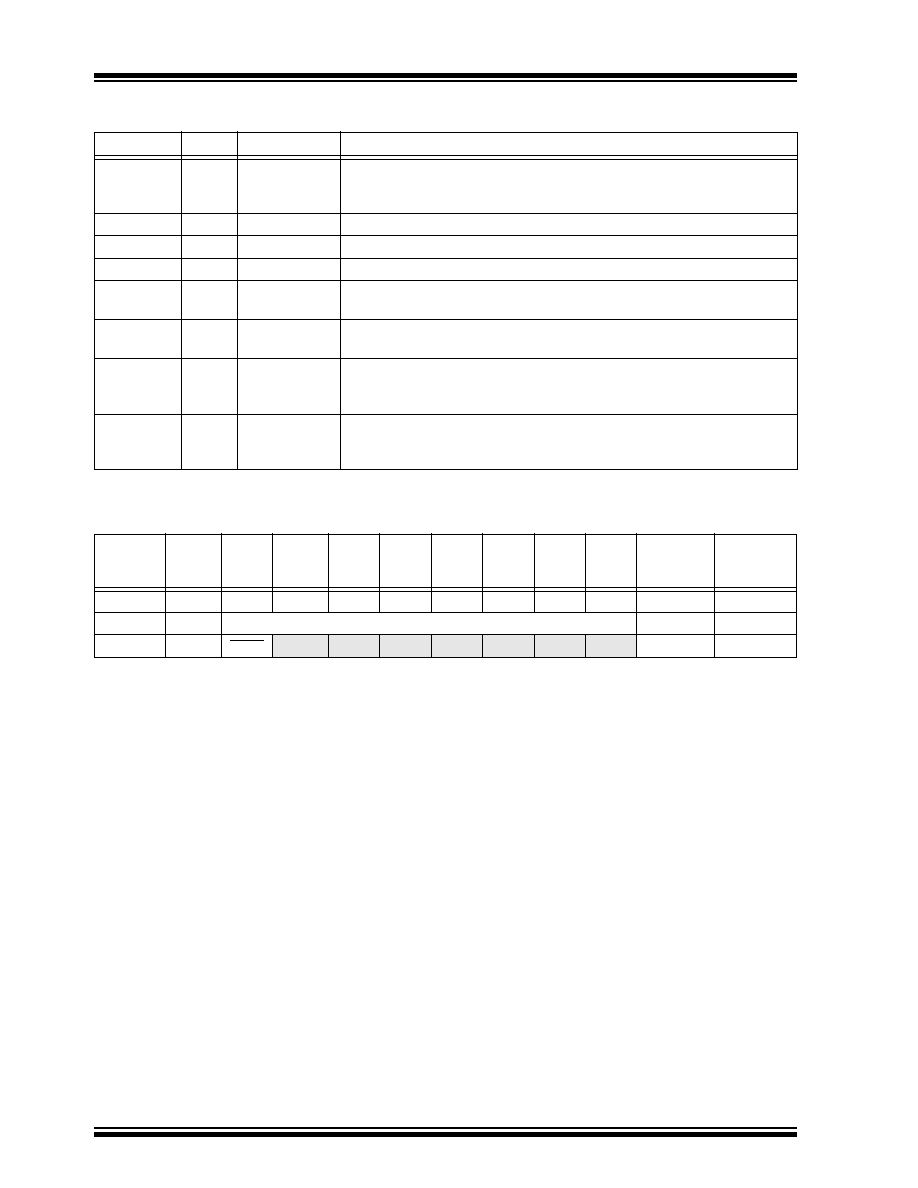
PIC16C9XX
DS30444E - page 34
©
1997 Microchip Technology Inc.
TABLE 5-3: PORTB FUNCTIONS
TABLE 5-4: SUMMARY OF REGISTERS ASSOCIATED WITH PORTB
Name
Bit#
Buffer
Function
RB0/INT
bit0
TTL/ST
Input/output pin or external interrupt input. Internal software
programmable weak pull-up. This buffer is a Schmitt Trigger input when
configured as the external interrupt.
RB1
bit1
TTL
Input/output pin. Internal software programmable weak pull-up.
RB2
bit2
TTL
Input/output pin. Internal software programmable weak pull-up.
RB3
bit3
TTL
Input/output pin. Internal software programmable weak pull-up.
RB4
bit4
TTL
Input/output pin (with interrupt on change). Internal software programmable
weak pull-up.
RB5
bit5
TTL
Input/output pin (with interrupt on change). Internal software programmable
weak pull-up.
RB6
bit6
TTL/ST
Input/output pin (with interrupt on change). Internal software programmable
weak pull-up. Serial programming clock. This buffer is a Schmitt Trigger
input when used in serial programming mode.
RB7
bit7
TTL/ST
Input/output pin (with interrupt on change). Internal software programmable
weak pull-up. Serial programming data. This buffer is a Schmitt Trigger input
when used in serial programming mode.
Legend: TTL = TTL input, ST = Schmitt Trigger input
Address
Name
Bit 7
Bit 6
Bit 5
Bit 4
Bit 3
Bit 2
Bit 1
Bit 0
Value on
Power-on
Reset
Value on all
other resets
06h, 106h
PORTB
RB7
RB6
RB5
RB4
RB3
RB2
RB1
RB0
xxxx xxxx
uuuu uuuu
86h, 186h
TRISB
PORTB Data Direction Control Register
1111 1111
1111 1111
81h, 181h
OPTION
RBPU
INTEDG
T0CS
T0SE
PSA
PS2
PS1
PS0
1111 1111
1111 1111
Legend:
x
= unknown,
u
= unchanged. Shaded cells are not used by PORTB.
©
1997 Microchip Technology Inc.
DS30444E - page 35
PIC16C9XX
5.3
PORTC and TRISC Register
PORTC is an 6-bit bi-directional port. Each pin is indi-
vidually configurable as an input or output through the
TRISC register. PORTC is multiplexed with several
peripheral functions (Table 5-5). PORTC pins have
Schmitt Trigger input buffers.
When enabling peripheral functions, care should be
taken in defining TRIS bits for each PORTC pin. Some
peripherals override the TRIS bit to make a pin an out-
put, while other peripherals override the TRIS bit to
make a pin an input. Since the TRIS bit override is in
effect while the peripheral is enabled, read-mod-
ify-write instructions (
BSF, BCF, XORWF
) with TRISC
as destination should be avoided. The user should refer
to the corresponding peripheral section for the correct
TRIS bit settings.
EXAMPLE 5-3:
INITIALIZING PORTC
BCF STATUS,RP0 ; Select Bank0
BCF STATUS,RP1
CLRF PORTC ; Initialize PORTC
BSF STATUS,RP0 ;
MOVLW 0xCF ; Value used to
; initialize data
; direction
MOVWF TRISC ; Set RC<3:0> as inputs
; RC<5:4> as outputs
; RC<7:6> always read 0
FIGURE 5-5:
PORTC BLOCK DIAGRAM
(PERIPHERAL OUTPUT
OVERRIDE)
Data Latch
RBPU
(2)
P
V
DD
Q
D
CK
Q
D
CK
Q
D
EN
Data bus
WR Port
WR TRIS
RD TRIS
RD Port
weak
pull-up
RD Port
RB0/INT
I/O
pin
(1)
TTL
Input
Buffer
Note 1: I/O pins have diode protection to V
DD
and V
SS
.
2: To enable weak pull-ups, set the appropriate TRIS bit(s)
and clear the RBPU bit (OPTION<7>).
Schmitt Trigger
Buffer
TRIS Latch
TABLE 5-5: PORTC FUNCTIONS
TABLE 5-6: SUMMARY OF REGISTERS ASSOCIATED WITH PORTC
Name
Bit#
Buffer Type
Function
RC0/T1OSO/T1CKI
bit0
ST
Input/output port pin or Timer1 oscillator output or Timer1 clock input
RC1/T1OSI
bit1
ST
Input/output port pin or Timer1 oscillator input
RC2/CCP1
bit2
ST
Input/output port pin or Capture input/Compare output/PWM output
RC3/SCK/SCL
bit3
ST
Input/output port pin or the synchronous serial clock for both SPI and
I
2
C modes.
RC4/SDI/SDA
bit4
ST
Input/output port pin or the SPI Data In (SPI mode) or data I/O (I
2
C
mode).
RC5/SDO
bit5
ST
Input/output port pin or Synchronous Serial Port data out
Legend: ST = Schmitt Trigger input
Address Name
Bit 7
Bit 6
Bit 5
Bit 4
Bit 3
Bit 2
Bit 1
Bit 0
Value on
Power-on
Reset
Value on all
other resets
07h
PORTC
--
--
RC5
RC4
RC3
RC2
RC1
RC0
--xx xxxx
--uu uuuu
87h
TRISC
--
--
PORTC Data Direction Control Register
--11 1111
--11 1111
Legend:
x
= unknown,
u
= unchanged,
-
= unimplemented, read as '0'. Shaded cells are not used by PORTC.
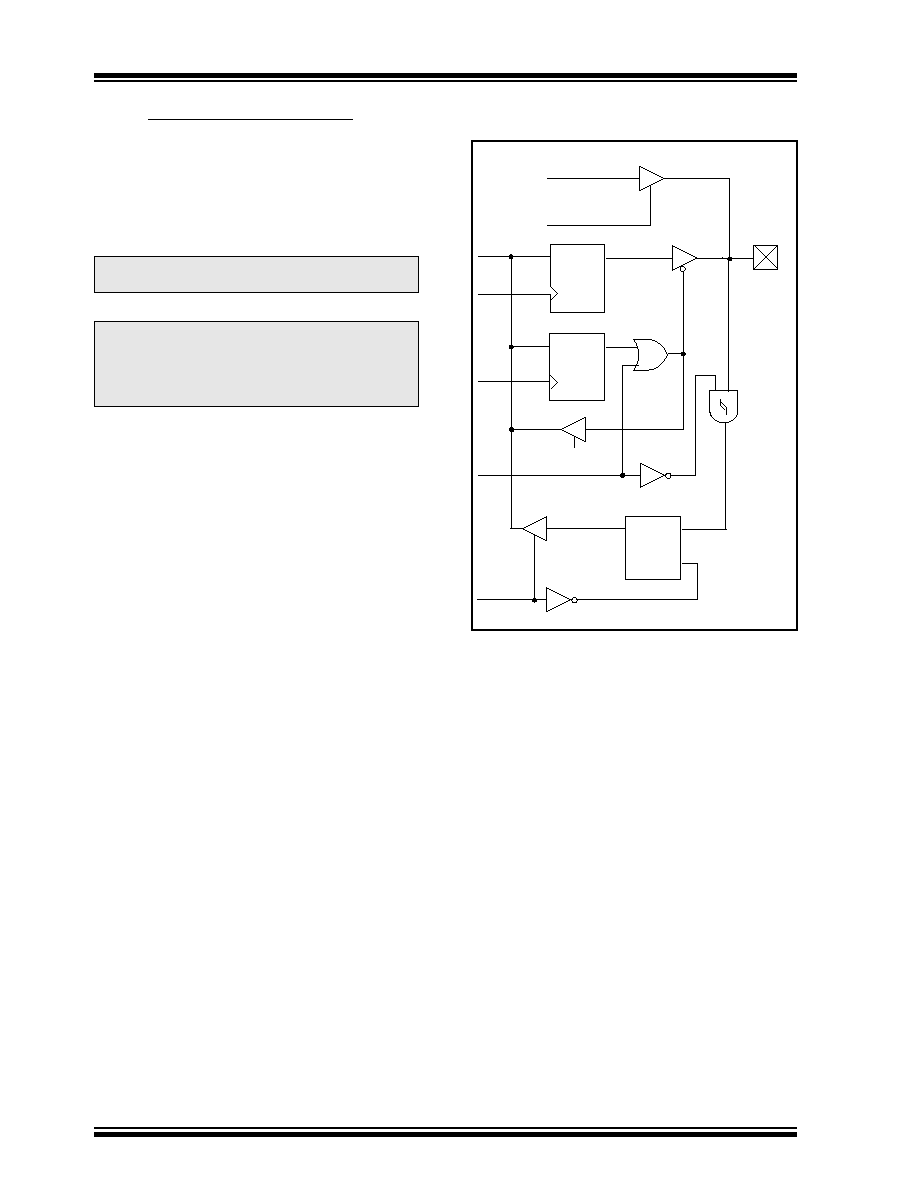
PIC16C9XX
DS30444E - page 36
©
1997 Microchip Technology Inc.
5.4
PORTD and TRISD Registers
PORTD is an 8-bit port with Schmitt Trigger input buff-
ers. The first five pins are configurable as general pur-
pose I/O pins or LCD segment drivers. Pins RD5, RD6
and RD7 can be digital inputs or LCD segment or com-
mon drivers.
TRISD controls the direction of pins RD0 through RD4
when PORTD is configured as a digital port.
EXAMPLE 5-4:
INITIALIZING PORTD
BCF STATUS,RP0 ;Select Bank2
BSF STATUS,RP1 ;
BCF LCDSE,SE29 ;Make RD<7:5> digital
BCF LCDSE,SE0 ;Make RD<4:0> digital
BSF STATUS,RP0 ;Select Bank1
BCF STATUS,RP1 ;
MOVLW 0x07 ;Make RD<4:0> outputs
MOVWF TRISD ;Make RD<7:5> inputs
Note:
On a Power-on Reset these pins are con-
figured as LCD segment drivers.
Note:
To configure the pins as a digital port, the
corresponding bits in the LCDSE register
must be cleared. Any bit set in the LCDSE
register overrides any bit settings in the
corresponding TRIS register.
FIGURE 5-6:
PORTD<4:0> BLOCK
DIAGRAM
Data Bus
WR
WR
RD
Data Latch
TRIS Latch
Schmitt
Trigger
input
buffer
Q
D
CK
Q
D
CK
EN
Q
D
EN
I/O pin
RD TRIS
LCDSE<n>
LCD
LCD Segment
Segment Data
Output Enable
PORT
TRIS
PORT
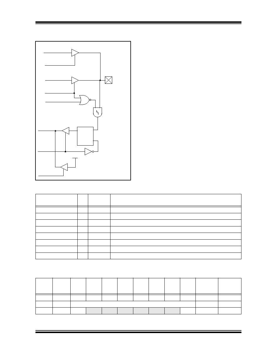
©
1997 Microchip Technology Inc.
DS30444E - page 37
PIC16C9XX
FIGURE 5-7:
PORTD<7:5> BLOCK
DIAGRAM
RD PORT
Schmitt
Trigger
input
buffer
EN
Q
D
EN
Digital Input/
LCDSE<n>
LCD
LCD Segment
LCD Output pin
LCD
LCD Common
Data Bus
RD TRIS
V
DD
Segment Data
Output Enable
Common Data
Output Enable
TABLE 5-7: PORTD FUNCTIONS
TABLE 5-8: SUMMARY OF REGISTERS ASSOCIATED WITH PORTD
Name
Bit#
Buffer
Type
Function
RD0/SEG00
bit0
ST
Input/output port pin or Segment Driver00
RD1/SEG01
bit1
ST
Input/output port pin or Segment Driver01
RD2/SEG02
bit2
ST
Input/output port pin or Segment Driver02
RD3/SEG03
bit3
ST
Input/output port pin or Segment Driver03
RD4/SEG04
bit4
ST
Input/output port pin or Segment Driver04
RD5/SEG29/COM3
bit5
ST
Digital input pin or Segment Driver29 or Common Driver3
RD6/SEG30/COM2
bit6
ST
Digital input pin or Segment Driver30 or Common Driver2
RD7/SEG31/COM1
bit7
ST
Digital input pin or Segment Driver31 or Common Driver1
Legend: ST = Schmitt Trigger input
Address Name
Bit 7
Bit 6
Bit 5
Bit 4
Bit 3
Bit 2
Bit 1
Bit 0
Value on
Power-on
Reset
Value on all
other resets
08h
PORTD
RD7
RD6
RD5
RD4
RD3
RD2
RD1
RD0
0000 0000
0000 0000
88h
TRISD
PORTD Data Direction Control Register
1111 1111
1111 1111
10Dh
LCDSE
SE29
SE27
SE20
SE16
SE12
SE9
SE5
SE0
1111 1111
1111 1111
Legend: Shaded cells are not used by PORTD.
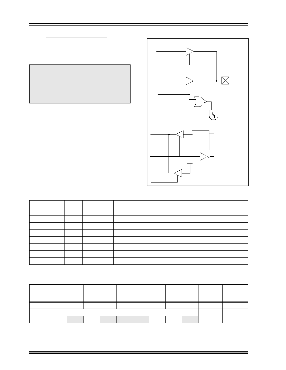
PIC16C9XX
DS30444E - page 38
©
1997 Microchip Technology Inc.
5.5
PORTE and TRISE Register
PORTE is an digital input only port. Each pin is multi-
plexed with an LCD segment driver. These pins have
Schmitt Trigger input buffers.
EXAMPLE 5-5:
INITIALIZING PORTE
BCF STATUS,RP0 ;Select Bank2
BSF STATUS,RP1 ;
BCF LCDSE,SE27 ;Make all PORTE
BCF LCDSE,SE5 ;and PORTG<7>
BCF LCDSE,SE9 ;digital inputs
Note 1: On a Power-on Reset these pins are con-
figured as LCD segment drivers.
Note 2: To configure the pins as a digital port, the
corresponding bits in the LCDSE register
must be cleared. Any bit set in the LCDSE
register overrides any bit settings in the
corresponding TRIS register.
FIGURE 5-8:
PORTE BLOCK DIAGRAM
RD PORT
Schmitt
Trigger
input
buffer
EN
Q
D
EN
Digital Input/
LCDSE<n>
LCD
LCD Segment
LCD Output pin
LCD
LCD Common
Data Bus
RD TRIS
V
DD
Segment Data
Output Enable
Common Data
Output Enable
TABLE 5-9: PORTE FUNCTIONS
TABLE 5-10: SUMMARY OF REGISTERS ASSOCIATED WITH PORTE
Name
Bit#
Buffer Type
Function
RE0/SEG05
bit0
ST
Digital input or Segment Driver05
RE1/SEG06
bit1
ST
Digital input or Segment Driver06
RE2/SEG07
bit2
ST
Digital input or Segment Driver07
RE3/SEG08
bit3
ST
Digital input or Segment Driver08
RE4/SEG09
bit4
ST
Digital input or Segment Driver09
RE5/SEG10
bit5
ST
Digital input or Segment Driver10
RE6/SEG11
bit6
ST
Digital input or Segment Driver11
RE7/SEG27
bit7
ST
Digital input or Segment Driver27 (not available on 64-pin devices)
Legend: ST = Schmitt Trigger input
Address Name
Bit 7
Bit 6
Bit 5
Bit 4
Bit 3
Bit 2
Bit 1
Bit 0
Value on
Power-on
Reset
Value on all
other resets
09h
PORTE
RE7
RE6
RE5
RE4
RE3
RE2
RE1
RE0
0000 0000
0000 0000
89h
TRISE
PORTE Data Direction Control Register
1111 1111
1111 1111
10Dh
LCDSE
SE29
SE27
SE20
SE16
SE12
SE9
SE5
SE0
1111 1111
1111 1111
Legend: Shaded cells are not used by PORTE.
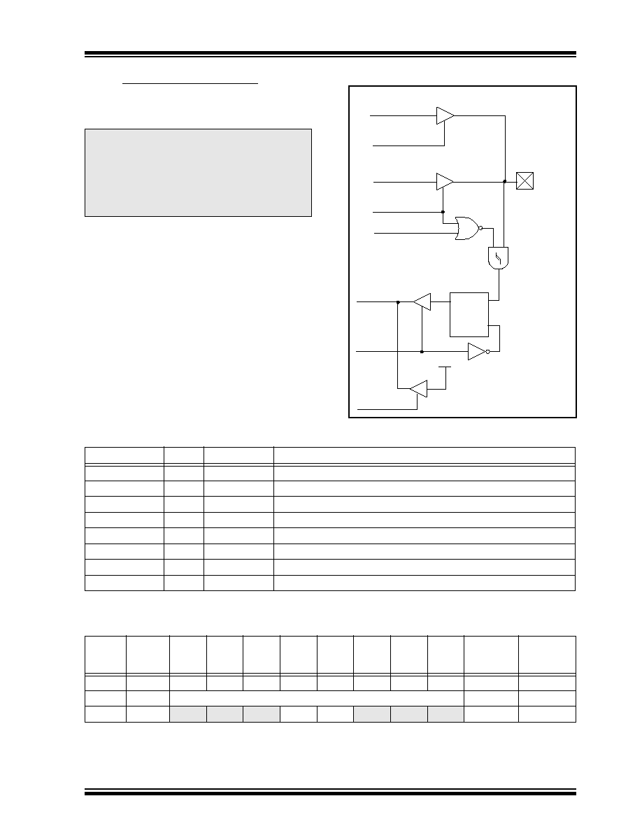
©
1997 Microchip Technology Inc.
DS30444E - page 39
PIC16C9XX
5.6
PORTF and TRISF Register
PORTF is an digital input only port. Each pin is multi-
plexed with an LCD segment driver. These pins have
Schmitt Trigger input buffers.
EXAMPLE 5-6:
INITIALIZING PORTF
BCF STATUS,RP0 ;Select Bank2
BSF STATUS,RP1 ;
BCF LCDSE,SE16 ;Make all PORTF
BCF LCDSE,SE12 ;digital inputs
Note 1: On a Power-on Reset these pins are con-
figured as LCD segment drivers.
Note 2: To configure the pins as a digital port, the
corresponding bits in the LCDSE register
must be cleared. Any bit set in the LCDSE
register overrides any bit settings in the
corresponding TRIS register.
FIGURE 5-9:
PORTF BLOCK DIAGRAM
RD PORT
Schmitt
Trigger
input
buffer
EN
Q
D
EN
Digital Input/
LCDSE<n>
LCD
LCD Segment
LCD Output pin
LCD
LCD Common
Data Bus
RD TRIS
V
DD
Segment Data
Output Enable
Common Data
Output Enable
TABLE 5-11: PORTF FUNCTIONS
TABLE 5-12: SUMMARY OF REGISTERS ASSOCIATED WITH PORTF
Name
Bit#
Buffer Type
Function
RF0/SEG12
bit0
ST
Digital input or Segment Driver12
RF1/SEG13
bit1
ST
Digital input or Segment Driver13
RF2/SEG14
bit2
ST
Digital input or Segment Driver14
RF3/SEG15
bit3
ST
Digital input or Segment Driver15
RF4/SEG16
bit4
ST
Digital input or Segment Driver16
RF5/SEG17
bit5
ST
Digital input or Segment Driver17
RF6/SEG18
bit6
ST
Digital input or Segment Driver18
RF7/SEG19
bit7
ST
Digital input or Segment Driver19
Legend: ST = Schmitt Trigger input
Address Name
Bit 7
Bit 6
Bit 5
Bit 4
Bit 3
Bit 2
Bit 1
Bit 0
Value on
Power-on
Reset
Value on all
other resets
107h
PORTF
RF7
RF6
RF5
RF4
RF3
RF2
RF1
RF0
0000 0000
0000 0000
187h
TRISF
PORTF Data Direction Control Register
1111 1111
1111 1111
10Dh
LCDSE
SE29
SE27
SE20
SE16
SE12
SE9
SE5
SE0
1111 1111
1111 1111
Legend: Shaded cells are not used by PORTF.
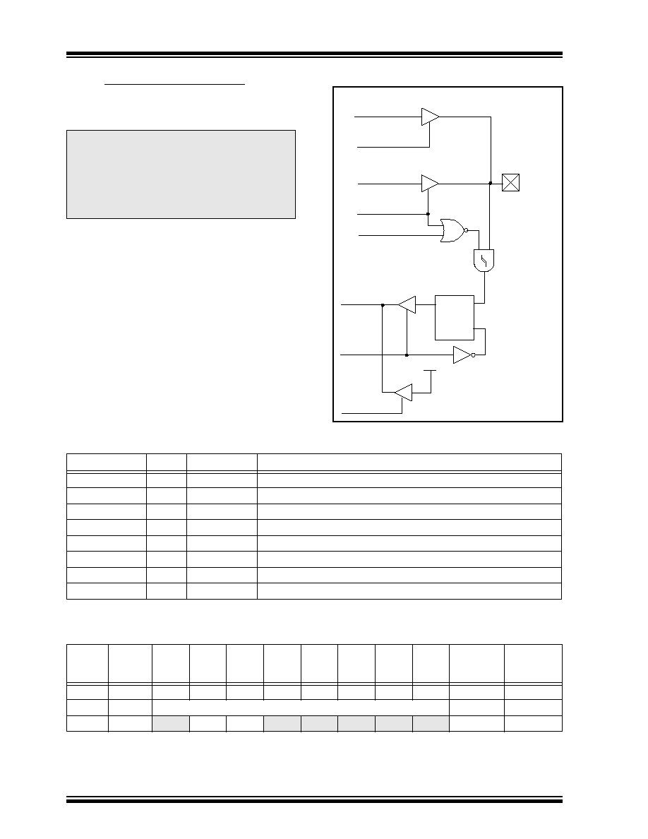
PIC16C9XX
DS30444E - page 40
©
1997 Microchip Technology Inc.
5.7
PORTG and TRISG Register
PORTG is an digital input only port. Each pin is multi-
plexed with an LCD segment driver. These pins have
Schmitt Trigger input buffers.
EXAMPLE 5-7:
INITIALIZING PORTG
BCF STATUS,RP0 ;Select Bank2
BSF STATUS,RP1 ;
BCF LCDSE,SE27 ;Make all PORTG
BCF LCDSE,SE20 ;and PORTE<7>
;digital inputs
Note 1: On a Power-on Reset these pins are con-
figured as LCD segment drivers.
Note 2: To configure the pins as a digital port, the
corresponding bits in the LCDSE register
must be cleared. Any bit set in the LCDSE
register overrides any bit settings in the
corresponding TRIS register.
FIGURE 5-10: PORTG BLOCK DIAGRAM
RD PORT
Schmitt
Trigger
input
buffer
EN
Q
D
EN
Digital Input/
LCDSE<n>
LCD
LCD Segment
LCD Output pin
LCD
LCD Common
Data Bus
RD TRIS
V
DD
Segment Data
Output Enable
Common Data
Output Enable
TABLE 5-13: PORTG FUNCTIONS
TABLE 5-14: SUMMARY OF REGISTERS ASSOCIATED WITH PORTG
Name
Bit#
Buffer Type
Function
RG0/SEG20
bit0
ST
Digital input or Segment Driver20
RG1/SEG21
bit1
ST
Digital input or Segment Driver21
RG2/SEG22
bit2
ST
Digital input or Segment Driver22
RG3/SEG23
bit3
ST
Digital input or Segment Driver23
RG4/SEG24
bit4
ST
Digital input or Segment Driver24
RG5/SEG25
bit5
ST
Digital input or Segment Driver25
RG6/SEG26
bit6
ST
Digital input or Segment Driver26
RG7/SEG28
bit7
ST
Digital input or Segment Driver28 (not available on 64-pin devices)
Legend: ST = Schmitt Trigger input
Address Name
Bit 7
Bit 6
Bit 5
Bit 4
Bit 3
Bit 2
Bit 1
Bit 0
Value on
Power-on
Reset
Value on all
other resets
108h
PORTG
RG7
RG6
RG5
RG4
RG3
RG2
RG1
RG0
0000 0000
0000 0000
188h
TRISG
PORTG Data Direction Control Register
1111 1111
1111 1111
10Dh
LCDSE
SE29
SE27
SE20
SE16
SE12
SE9
SE5
SE0
1111 1111
1111 1111
Legend: Shaded cells are not used by PORTG.
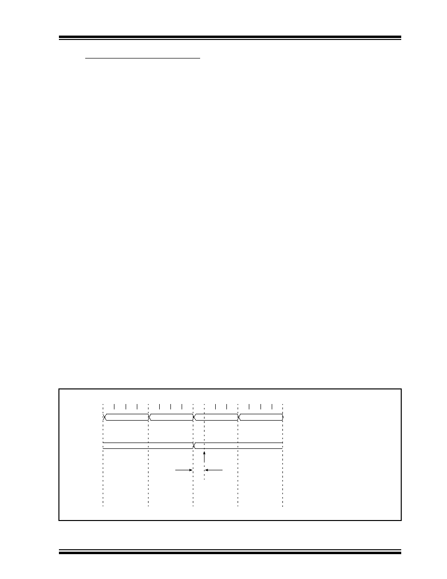
©
1997 Microchip Technology Inc.
DS30444E - page 41
PIC16C9XX
5.8
I/O Programming Considerations
5.8.1
BI-DIRECTIONAL I/O PORTS
Any instruction which writes, operates internally as a
read followed by a write operation. The
BCF
and
BSF
instructions, for example, read the register into the
CPU, execute the bit operation and write the result back
to the register. Caution must be used when these
instructions are applied to a port with both inputs and
outputs defined. For example, a
BSF
operation on bit5
of PORTB will cause all eight bits of PORTB to be read
into the CPU. Then the
BSF
operation takes place on
bit5 and PORTB is written to the output latches. If
another bit of PORTB is used as a bi-directional I/O pin
(e.g., bit0) and it is defined as an input at this time, the
input signal present on the pin itself would be read into
the CPU and rewritten to the data latch of this particular
pin, overwriting the previous content. As long as the pin
stays in the input mode, no problem occurs. However, if
bit0 is switched into output mode later on, the contents
of the data latch may now be unknown.
Reading the port register, reads the values of the port
pins. Writing to the port register writes the value to the
port latch. When using read-modify-write instructions
(ex.
BCF, BSF
) on a port, the value of the port pins is
read, the desired operation is done to this value, and
this value is then written to the port latch.
Example 5-8 shows the effect of two sequential
read-modify-write instructions on an I/O port.
EXAMPLE 5-8:
READ-MODIFY-WRITE
INSTRUCTIONS ON AN I/O
PORT
;Initial PORT settings: PORTB<7:4> Inputs
; PORTB<3:0> Outputs
;PORTB<7:6> have external pull-ups and are
;not connected to other circuitry
;
; PORT latch PORT pins
; ---------- ---------
BCF PORTB, 7 ; 01pp pppp 11pp pppp
BCF PORTB, 6 ; 10pp pppp 11pp pppp
BCF STATUS, RP1 ;
BSF STATUS, RP0 ;
BCF TRISB, 7 ; 10pp pppp 11pp pppp
BCF TRISB, 6 ; 10pp pppp 10pp pppp
;
;Note that the user may have expected the
;pin values to be 00pp ppp. The 2nd BCF
;caused RB7 to be latched as the pin value
;(high).
A pin actively outputting a Low or High should not be
driven from external devices at the same time in order
to change the level on this pin ("wired-or", "wired-and").
The resulting high output currents may damage the
chip.
5.8.2
SUCCESSIVE OPERATIONS ON I/O PORTS
The actual write to an I/O port happens at the end of an
instruction cycle, whereas for reading, the data must be
valid at the beginning of the instruction cycle
(Figure
5-11).
Therefore, care must be exercised if a
write followed by a read operation is carried out on the
same I/O port. The sequence of instructions should be
such to allow the pin voltage to stabilize (load depen-
dent) before the next instruction which causes that file
to be read into the CPU is executed. Otherwise, the
previous state of that pin may be read into the CPU
rather than the new state. When in doubt, it is better to
separate these instructions with a
NOP
or another
instruction not accessing this I/O port.
FIGURE 5-11: SUCCESSIVE I/O OPERATION
PC
PC + 1
PC + 2
PC + 3
Q1 Q2 Q3 Q4
Q1 Q2 Q3 Q4 Q1 Q2 Q3 Q4
Q1 Q2 Q3 Q4
Instruction
fetched
RB7:RB0
MOVWF PORTB
write to
PORTB
NOP
Port pin
sampled here
NOP
MOVF PORTB,W
Instruction
executed
MOVWF PORTB
write to
PORTB
NOP
MOVF PORTB,W
PC
T
PD
Note:
This example shows a write to PORTB
followed by a read from PORTB.
Note that:
data setup time = (0.25T
CY
- T
PD
)
where T
CY
= instruction cycle
T
PD
= propagation delay
Therefore, at higher clock frequencies,
a write followed by a read may be prob-
lematic.

PIC16C9XX
DS30444E - page 42
©
1997 Microchip Technology Inc.
NOTES:

©
1997 Microchip Technology Inc.
DS30444E - page 43
PIC16C9XX
6.0
OVERVIEW OF TIMER
MODULES
Each module can generate an interrupt to indicate that
an event has occurred (e.g. timer overflow). Each of
these modules is explained in full detail in the following
sections. The timer modules are:
· Timer0 Module (Section 7.0)
· Timer1 Module (Section 8.0)
· Timer2 Module (Section 9.0)
6.1
Timer0 Overview
The Timer0 module is a simple 8-bit timer/counter. The
clock source can be either the internal system clock
(Fosc/4) or an external clock. When the clock source is
an external clock, the Timer0 module can be selected
to increment on either the rising or falling edge.
The Timer0 module also has a programmable prescaler
option. This prescaler can be assigned to either the
Timer0 module or the Watchdog Timer. Bit PSA
(OPTION<3>) assigns the prescaler, and bits PS2:PS0
(OPTION<2:0>) determine the prescaler value. Timer0
can increment at the following rates: 1:1 when pres-
caler assigned to Watchdog timer, 1:2, 1:4, 1:8, 1:16,
1:32, 1:64, 1:128, and 1:256.
Synchronization of the external clock occurs after the
prescaler. When the prescaler is used, the external
clock frequency may be higher then the device's fre-
quency. The maximum frequency is 50 MHz, given the
high and low time requirements of the clock.
6.2
Timer1 Overview
Timer1 is a 16-bit timer/counter. The clock source can
be either the internal system clock (Fosc/4), an external
clock, or an external crystal. Timer1 can operate as
either a timer or a counter. When operating as a counter
(external clock source), the counter can either operate
synchronized to the device or asynchronously to the
device. Asynchronous operation allows Timer1 to oper-
ate during sleep, which is useful for applications that
require a real-time clock as well as the power savings
of SLEEP mode.
Timer1 also has a prescaler option which allows Timer1
to increment at the following rates: 1:1, 1:2, 1:4, and
1:8. Timer1 can be used in conjunction with the Cap-
ture/Compare/PWM module. When used with a CCP
module, Timer1 is the time-base for 16-bit capture or
the 16-bit compare and must be synchronized to the
device. Timer1 oscillator is also one of the clock
sources for the LCD module.
6.3
Timer2 Overview
Timer2 is an 8-bit timer with a programmable prescaler
and postscaler, as well as an 8-bit period register
(PR2). Timer2 can be used with the CCP1 module (in
PWM mode) as well as the clock source for the Syn-
chronous Serial Port (SSP). The prescaler option
allows Timer2 to increment at the following rates: 1:1,
1:4, 1:16.
The postscaler allows the TMR2 register to match the
period register (PR2) a programmable number of times
before generating an interrupt. The postscaler can be
programmed from 1:1 to 1:16 (inclusive).
6.4
CCP Overview
The CCP module can operate in one of these three
modes: 16-bit capture, 16-bit compare, or up to 10-bit
Pulse Width Modulation (PWM).
Capture mode captures the 16-bit value of TMR1 into
the CCPR1H:CCPR1L register pair. The capture event
can be programmed for either the falling edge, rising
edge, fourth rising edge, or the sixteenth rising edge of
the CCP1 pin.
Compare mode compares the TMR1H:TMR1L register
pair to the CCPR1H:CCPR1L register pair. When a
match occurs an interrupt can be generated, and the
output pin CCP1 can be forced to given state (High or
Low), TMR1 can be reset and start A/D conversion.
This depends on the control bits CCP1M3:CCP1M0.
PWM mode compares the TMR2 register to a 10-bit
duty cycle register (CCPR1H:CCPR1L<5:4>) as well
as to an 8-bit period register (PR2). When the TMR2
register = Duty Cycle register, the CCP1 pin will be
forced low. When TMR2 = PR2, TMR2 is cleared to 00h,
an interrupt can be generated, and the CCP1 pin (if an
output) will be forced high.

PIC16C9XX
DS30444E - page 44
©
1997 Microchip Technology Inc.
NOTES:
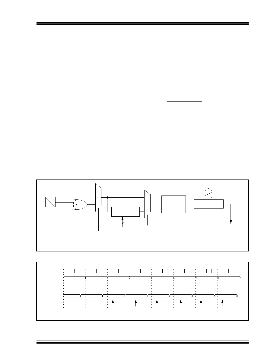
©
1997 Microchip Technology Inc.
DS30444E - page 45
PIC16C9XX
7.0
TIMER0 MODULE
The Timer0 module has the following features:
· 8-bit timer/counter
· Readable and writable
· 8-bit software programmable prescaler
· Internal or external clock select
· Interrupt on overflow from FFh to 00h
· Edge select for external clock
Figure 7-1 is a simplified block diagram of the Timer0
module.
Timer mode is selected by clearing bit T0CS
(OPTION<5>). In timer mode, the Timer0 module will
increment every instruction cycle (without prescaler). If
the TMR0 register is written, the increment is inhibited
for the following two instruction cycles (Figure 7-2 and
Figure 7-3). The user can work around this by writing
an adjusted value to the TMR0 register.
Counter mode is selected by setting bit T0CS
(OPTION<5>). In counter mode Timer0 will increment
either on every rising or falling edge of pin RA4/T0CKI.
The incrementing edge is determined by the Timer0
Source Edge Select bit T0SE (OPTION<4>). Clearing
bit T0SE selects the rising edge. Restrictions on the
external clock input are discussed in detail in
Section
7.2.
The prescaler is mutually exclusively shared between
the Timer0 module and the Watchdog Timer. The pres-
caler assignment is controlled in software by control bit
PSA (OPTION<3>). Clearing bit PSA will assign the
prescaler to the Timer0 module. The prescaler is not
readable or writable. When the prescaler is assigned to
the Timer0 module, prescale values of 1:2, 1:4, ...,
1:256 are selectable. Section 7.3 details the operation
of the prescaler.
7.1
Timer0 Interrupt
The TMR0 interrupt is generated when the TMR0 reg-
ister overflows from FFh to 00h. This overflow sets bit
T0IF (INTCON<2>). The interrupt can be masked by
clearing bit T0IE (INTCON<5>). Bit T0IF must be
cleared in software by the Timer0 module interrupt ser-
vice routine before re-enabling this interrupt. The TMR0
interrupt cannot awaken the processor from SLEEP
since the timer is shut off during SLEEP. Figure 7-4 dis-
plays the Timer0 interrupt timing.
FIGURE 7-1:
TIMER0 BLOCK DIAGRAM
FIGURE 7-2:
TIMER0 TIMING: INTERNAL CLOCK/NO PRESCALE
Note 1: T0CS, T0SE, PSA, PS2:PS0 (OPTION<5:0>).
2: The prescaler is shared with Watchdog Timer (refer to Figure 7-6 for detailed block diagram).
RA4/T0CKI
T0SE
0
1
1
0
pin
T0CS
F
OSC
/4
Programmable
Prescaler
Sync with
Internal
clocks
TMR0
PSout
(2 cycle delay)
PSout
Data bus
8
PSA
PS2, PS1, PS0
Set interrupt
flag bit T0IF
on overflow
3
PC-1
Q1 Q2 Q3 Q4 Q1 Q2 Q3 Q4 Q1 Q2 Q3 Q4 Q1 Q2 Q3 Q4 Q1 Q2 Q3 Q4 Q1 Q2 Q3 Q4 Q1 Q2 Q3 Q4 Q1 Q2 Q3 Q4
PC
(Program
Counter)
Instruction
Fetch
TMR0
PC
PC+1
PC+2
PC+3
PC+4
PC+5
PC+6
T0
T0+1
T0+2
NT0
NT0
NT0
NT0+1
NT0+2
T0
MOVWF TMR0
MOVF TMR0,W
MOVF TMR0,W
MOVF TMR0,W
MOVF TMR0,W
MOVF TMR0,W
Write TMR0
executed
Read TMR0
reads NT0
Read TMR0
reads NT0
Read TMR0
reads NT0
Read TMR0
reads NT0 + 1
Read TMR0
reads NT0 + 2
Instruction
Executed
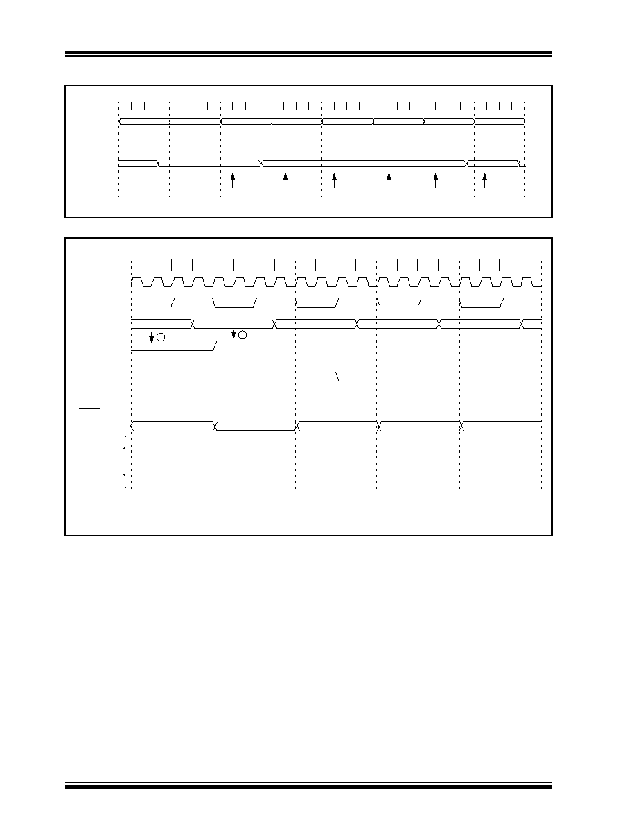
PIC16C9XX
DS30444E - page 46
©
1997 Microchip Technology Inc.
FIGURE 7-3:
TIMER0 TIMING: INTERNAL CLOCK/PRESCALE 1:2
FIGURE 7-4:
TIMER0 INTERRUPT TIMING
PC+6
PC-1
Q1 Q2 Q3 Q4 Q1 Q2 Q3 Q4 Q1 Q2 Q3 Q4 Q1 Q2 Q3 Q4 Q1 Q2 Q3 Q4 Q1 Q2 Q3 Q4 Q1 Q2 Q3 Q4 Q1 Q2 Q3 Q4
PC
(Program
Counter)
Instruction
Fetch
TMR0
PC
PC+1
PC+2
PC+3
PC+4
PC+5
PC+6
T0
NT0+1
MOVWF TMR0
MOVF TMR0,W
MOVF TMR0,W
MOVF TMR0,W
MOVF TMR0,W
MOVF TMR0,W
Write TMR0
executed
Read TMR0
reads NT0
Read TMR0
reads NT0
Read TMR0
reads NT0
Read TMR0
reads NT0
Read TMR0
reads NT0 + 1
T0+1
NT0
Instruction
Execute
Q2
Q1
Q3
Q4
Q2
Q1
Q3
Q4
Q2
Q1
Q3
Q4
Q2
Q1
Q3
Q4
Q2
Q1
Q3
Q4
1
1
OSC1
CLKOUT(3)
Timer0
T0IF bit
(INTCON<2>)
FEh
GIE bit
(INTCON<7>)
INSTRUCTION
PC
Instruction
fetched
PC
PC +1
PC +1
0004h
0005h
Instruction
executed
Inst (PC)
Inst (PC-1)
Inst (PC+1)
Inst (PC)
Inst (0004h)
Inst (0005h)
Inst (0004h)
Dummy cycle
Dummy cycle
FFh
00h
01h
02h
Note 1: Interrupt flag bit T0IF is sampled here (every Q1).
2: Interrupt latency = 4T
CY
where T
CY
= instruction cycle time.
3: CLKOUT is available only in RC oscillator mode.
FLOW
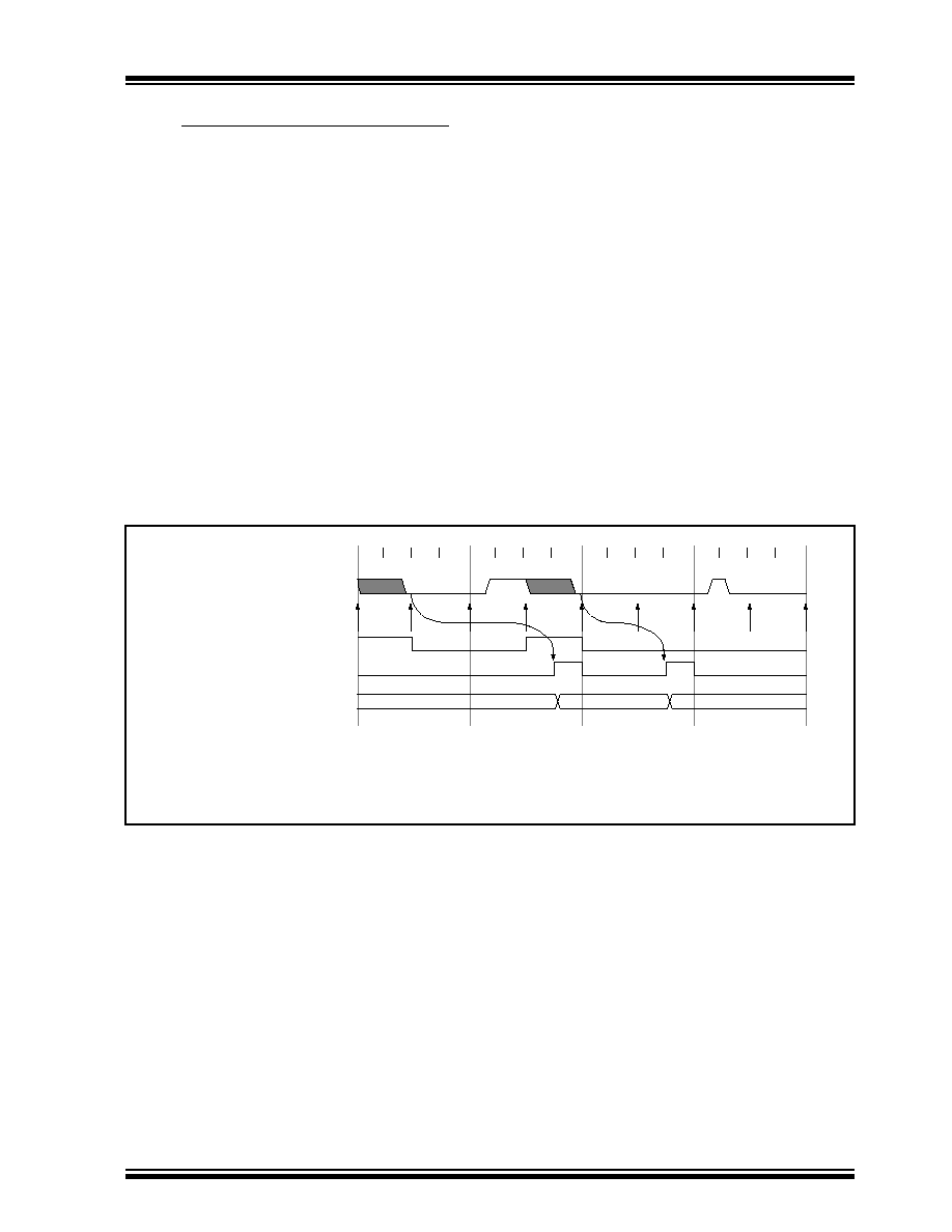
©
1997 Microchip Technology Inc.
DS30444E - page 47
PIC16C9XX
7.2
Using Timer0 with an External Clock
When an external clock input is used for Timer0, it must
meet certain requirements. The requirements ensure
the external clock can be synchronized with the internal
phase clock (T
OSC
). Also, there is a delay in the actual
incrementing of Timer0 after synchronization.
7.2.1
EXTERNAL CLOCK SYNCHRONIZATION
When no prescaler is used, the external clock input is
the same as the prescaler output. The synchronization
of T0CKI with the internal phase clocks is accom-
plished by sampling the prescaler output on the Q2 and
Q4 cycles of the internal phase clocks (Figure 7-5).
Therefore, it is necessary for T0CKI to be high for at
least 2Tosc (and a small RC delay of 20 ns) and low for
at least 2Tosc (and a small RC delay of 20 ns). Refer to
the electrical specification of the desired device.
When a prescaler is used, the external clock input is
divided by the asynchronous ripple-counter type pres-
caler so that the prescaler output is symmetrical. For
the external clock to meet the sampling requirement,
the ripple-counter must be taken into account. There-
fore, it is necessary for T0CKI to have a period of at
least 4Tosc (and a small RC delay of 40 ns) divided by
the prescaler value. The only requirement on T0CKI
high and low time is that they do not violate the mini-
mum pulse width requirement of 10 ns. Refer to param-
eters 40, 41 and 42 in the electrical specification of the
desired device.
7.2.2
TMR0 INCREMENT DELAY
Since the prescaler output is synchronized with the
internal clocks, there is a small delay from the time the
external clock edge occurs to the time the Timer0 mod-
ule is actually incremented. Figure 7-5 shows the delay
from the external clock edge to the timer incrementing.
FIGURE 7-5:
TIMER0 TIMING WITH EXTERNAL CLOCK
Q1
Q2 Q3 Q4
Q1 Q2 Q3 Q4
Q1 Q2 Q3 Q4
Q1 Q2 Q3 Q4
External Clock Input or
Prescaler output
(2)
External Clock/Prescaler
Output after sampling
Increment Timer0 (Q4)
Timer0
T0
T0 + 1
T0 + 2
Small pulse
misses sampling
Note 1: Delay from clock input change to Timer0 increment is 3Tosc to 7Tosc. (Duration of Q = Tosc).
Therefore, the error in measuring the interval between two edges on Timer0 input =
±
4Tosc max.
2: External clock if no prescaler selected, Prescaler output otherwise.
3: The arrows indicate the points in time where sampling occurs.
(3)
(1)
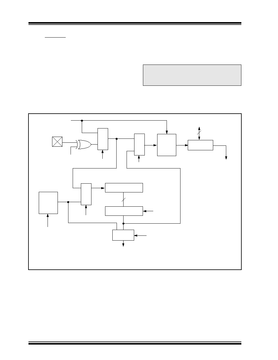
PIC16C9XX
DS30444E - page 48
©
1997 Microchip Technology Inc.
7.3
Prescaler
An 8-bit counter is available as a prescaler for the
Timer0 module, or as a postscaler for the Watchdog
Timer (Figure 7-6). For simplicity, this counter is being
referred to as "prescaler" throughout this data sheet.
Note that the prescaler may be used by either the
Timer0 module or the WDT but not both. Thus, a pres-
caler assignment for the Timer0 module means that
there is no prescaler for the Watchdog Timer, and
vice-versa.
The PSA and PS2:PS0 bits (OPTION<3:0>) determine
the prescaler assignment and prescale ratio.
When assigned to the Timer0 module, all instructions
writing to the TMR0 register (e.g.
CLRF 1, MOVWF 1,
BSF 1,x
....etc.) will clear the prescaler count. When
assigned to WDT, a
CLRWDT
instruction will clear the
prescaler count along with the Watchdog Timer. The
prescaler is not readable or writable.
Note:
Writing to TMR0 when the prescaler is
assigned to Timer0 will clear the prescaler
count, but will not change the prescaler
assignment.
FIGURE 7-6:
BLOCK DIAGRAM OF THE TIMER0/WDT PRESCALER
RA4/T0CKI
T0SE
pin
M
U
X
CLKOUT (=Fosc/4)
SYNC
2
Cycles
TMR0 reg
8-bit Prescaler
8 - to - 1MUX
M
U
X
M U X
Watchdog
Timer
PSA
0
1
0
1
WDT
Time-out
PS2:PS0
8
Note: T0CS, T0SE, PSA, PS2:PS0 are (OPTION<5:0>).
PSA
WDT Enable bit
M
U
X
0
1
0
1
Data Bus
Set flag bit T0IF
on Overflow
8
PSA
T0CS
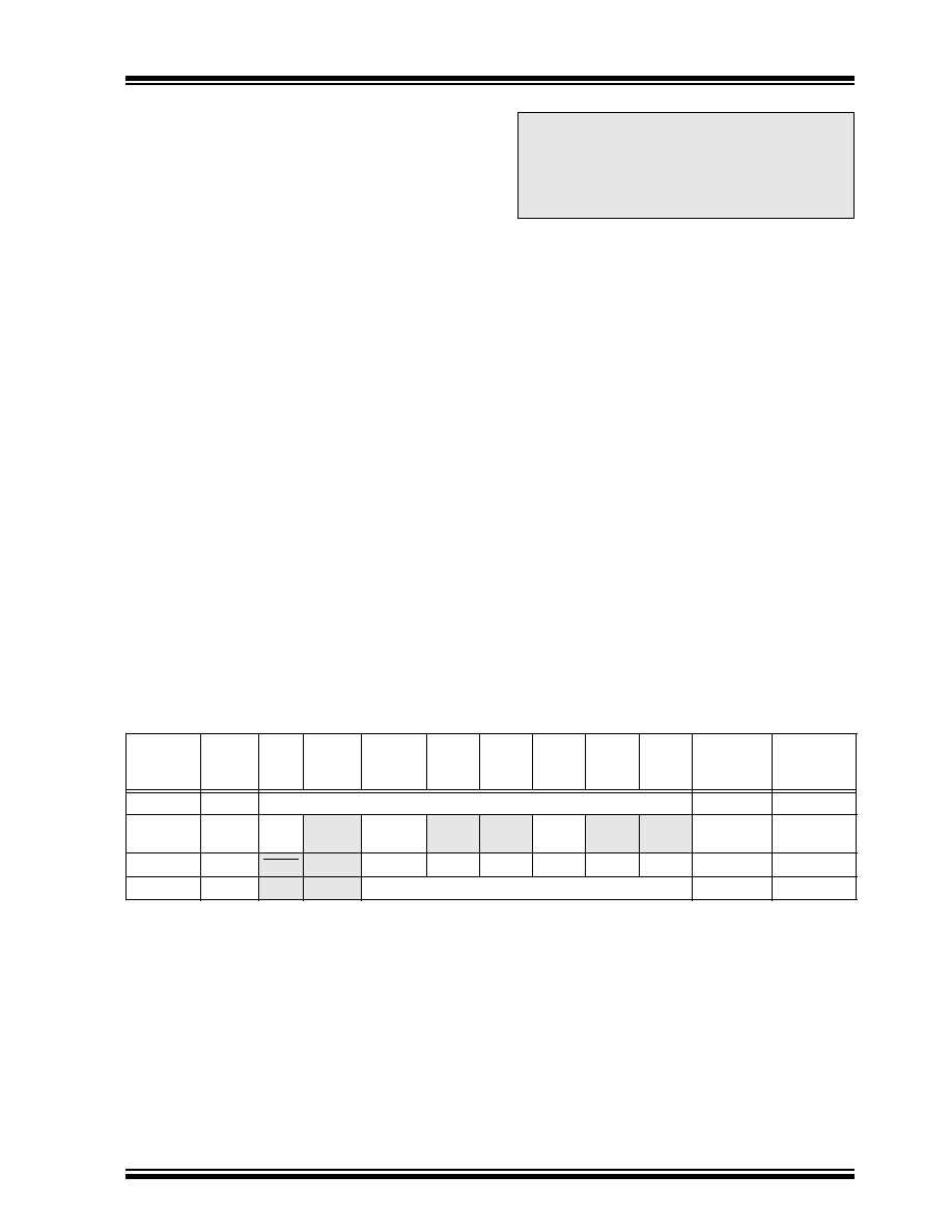
©
1997 Microchip Technology Inc.
DS30444E - page 49
PIC16C9XX
7.3.1
SWITCHING PRESCALER ASSIGNMENT
The prescaler assignment is fully under software con-
trol, i.e., it can be changed "on the fly" during program
execution.
Note:
To avoid an unintended device RESET, the
following instruction sequence (shown in
Example 7-1) must be executed when
changing the prescaler assignment from
Timer0 to the WDT. This precaution must
be followed even if the WDT is disabled.
EXAMPLE 7-1:
CHANGING PRESCALER (TIMER0
WDT)
To change prescaler from the WDT to the Timer0 mod-
ule use the precaution shown in Example 7-2.
EXAMPLE 7-2:
CHANGING PRESCALER (WDT
TIMER0)
CLRWDT ;Clear WDT and prescaler
BSF STATUS, RP0 ;Select Bank1
MOVLW b'xxxx0xxx' ;Select TMR0, new prescale value and
MOVWF OPTION_REG ;clock source
BCF STATUS, RP0 ;Select Bank0
TABLE 7-1: REGISTERS ASSOCIATED WITH TIMER0
1) BSF STATUS, RP0 ;Select Bank1
Lines 2 and 3 do NOT have to
be included if the final desired
prescale value is other than 1:1.
If 1:1 is final desired value, then
a temporary prescale value is
set in lines 2 and 3 and the final
prescale value will be set in lines
10 and 11.
2) MOVLW b'xx0x0xxx' ;Select clock source and prescale value of
3) MOVWF OPTION_REG ;other than 1:1
4) BCF STATUS, RP0 ;Select Bank0
5) CLRF TMR0 ;Clear TMR0 and prescaler
6) BSF STATUS, RP1 ;Select Bank1
7) MOVLW b'xxxx1xxx' ;Select WDT, do not change prescale value
8) MOVWF OPTION_REG ;
9) CLRWDT ;Clears WDT and prescaler
10) MOVLW b'xxxx1xxx' ;Select new prescale value and WDT
11) MOVWF OPTION_REG ;
12) BCF STATUS, RP0 ;Select Bank0
Address
Name
Bit 7
Bit 6
Bit 5
Bit 4
Bit 3
Bit 2
Bit 1
Bit 0
Value on
Power-on
Reset
Value on all
other resets
01h, 101h
TMR0
Timer0 module's register
xxxx xxxx
uuuu uuuu
0Bh, 8Bh,
10Bh, 18Bh
INTCON
GIE
PEIE
T0IE
INTE
RBIE
T0IF
INTF
RBIF
0000 000x
0000 000u
81h, 181h
OPTION RBPU INTEDG
T0CS
T0SE
PSA
PS2
PS1
PS0
1111 1111
1111 1111
85h
TRISA
--
--
PORTA Data Direction Control Register
--11 1111
--11 1111
Legend:
x
= unknown,
u
= unchanged,
-
= unimplemented locations read as '0'. Shaded cells are not used by Timer0.

PIC16C9XX
DS30444E - page 50
©
1997 Microchip Technology Inc.
NOTES:
©
1997 Microchip Technology Inc.
DS30444E - page 51
PIC16C9XX
8.0
TIMER1 MODULE
Timer1 is a 16-bit timer/counter consisting of two 8-bit
registers (TMR1H and TMR1L) which are readable and
writable. The TMR1 Register pair (TMR1H:TMR1L)
increments from 0000h to FFFFh and rolls over to
0000h. The TMR1 Interrupt, if enabled, is generated on
overflow which is latched in interrupt flag bit TMR1IF
(PIR1<0>). This interrupt can be enabled/disabled by
setting/clearing TMR1 interrupt enable bit TMR1IE
(PIE1<0>).
Timer1 can operate in one of two modes:
· As a timer
· As a counter
The operating mode is determined by the clock select
bit, TMR1CS (T1CON<1>).
In timer mode, Timer1 increments every instruction
cycle. In counter mode, it increments on every rising
edge of the external clock input.
Timer1 can be turned on and off using the control bit
TMR1ON (T1CON<0>).
Timer1 also has an internal "reset input". This reset can
be generated by the CCP module (Section 10.0).
Figure 8-1 shows the Timer1 control register.
When the Timer1 oscillator is enabled (T1OSCEN is
set), the RC1/T1OSI and RC0/T1OSO/T1CKI pins
become inputs.
FIGURE 8-1:
T1CON: TIMER1 CONTROL REGISTER
(ADDRESS 10h)
U-0
U-0
R/W-0
R/W-0
R/W-0
R/W-0
R/W-0
R/W-0
--
--
T1CKPS1 T1CKPS0 T1OSCEN
T1SYNC
TMR1CS TMR1ON
R
= Readable bit
W = Writable bit
U
= Unimplemented bit,
read as `0'
- n = Value at POR reset
bit7
bit0
bit 7-6:
Unimplemented: Read as '0'
bit 5-4: T1CKPS1:T1CKPS0: Timer1 Input Clock Prescale Select bits
11
= 1:8 Prescale value
10
= 1:4 Prescale value
01
= 1:2 Prescale value
00
= 1:1 Prescale value
bit 3:
T1OSCEN: Timer1 Oscillator Enable Control bit
1 = Oscillator is enabled
0 = Oscillator is shut off
Note: The oscillator inverter and feedback resistor are turned off to eliminate power drain
bit 2:
T1SYNC: Timer1 External Clock Input Synchronization Control bit
TMR1CS = 1
1 = Do not synchronize external clock input
0 = Synchronize external clock input
TMR1CS = 0
This bit is ignored. Timer1 uses the internal clock when TMR1CS = 0.
bit 1:
TMR1CS: Timer1 Clock Source Select bit
1 = External clock from pin T1CKI (on the rising edge)
0 = Internal clock (Fosc/4)
bit 0:
TMR1ON: Timer1 On bit
1 = Enables Timer1
0 = Stops Timer1
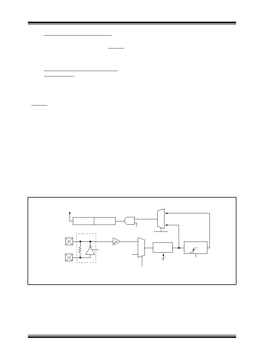
PIC16C9XX
DS30444E - page 52
©
1997 Microchip Technology Inc.
8.1
Timer1 Operation in Timer Mode
Timer mode is selected by clearing the TMR1CS
(T1CON<1>) bit. In this mode, the input clock to the
timer is Fosc/4. The synchronize control bit T1SYNC
(T1CON<2>) has no effect since the internal clock is
always in sync.
8.2
Timer1 Operation in Synchronized
Counter Mode
Counter mode is selected by setting bit TMR1CS. In
this mode the timer increments on every rising edge of
clock input on pin RC1/T1OSI when bit T1OSCEN is
set or pin RC0/T1OSO/T1CKI when bit T1OSCEN is
cleared.
If T1SYNC is cleared, then the external clock input is
synchronized with internal phase clocks. The synchro-
nization is done after the prescaler stage. The pres-
caler is an asynchronous ripple-counter.
In this configuration, during SLEEP mode, Timer1 will
not increment even if the external clock is present,
since the synchronization circuit is shut off. The pres-
caler however will continue to increment.
8.2.1
EXTERNAL CLOCK INPUT TIMING FOR
SYNCHRONIZED COUNTER MODE
When an external clock input is used for Timer1 in syn-
chronized counter mode, it must meet certain require-
ments. The external clock requirement is due to
internal phase clock (Tosc) synchronization. Also, there
is a delay in the actual incrementing of TMR1 after syn-
chronization.
When the prescaler is 1:1, the external clock input is
the same as the prescaler output. The synchronization
of T1CKI with the internal phase clocks is accom-
plished by sampling the prescaler output on the Q2 and
Q4 cycles of the internal phase clocks. Therefore, it is
necessary for T1CKI to be high for at least 2Tosc (and
a small RC delay of 20 ns) and low for at least 2Tosc
(and a small RC delay of 20 ns). Refer to the appropri-
ate electrical specifications, parameters 45, 46, and 47.
When a prescaler other than 1:1 is used, the external
clock input is divided by the asynchronous rip-
ple-counter type prescaler so that the prescaler output
is symmetrical. In order for the external clock to meet
the sampling requirement, the ripple-counter must be
taken into account. Therefore, it is necessary for T1CKI
to have a period of at least 4Tosc (and a small RC delay
of 40 ns) divided by the prescaler value. The only
requirement on T1CKI high and low time is that they do
not violate the minimum pulse width requirements of
10 ns). Refer to the appropriate electrical specifica-
tions, parameters 40, 42, 45, 46, and 47.
FIGURE 8-2:
TIMER1 BLOCK DIAGRAM
TMR1H
TMR1L
T1OSC
T1SYNC
TMR1CS
T1CKPS1:T1CKPS0
SLEEP input
T1OSCEN
Enable
Oscillator
(1)
Fosc/4
Internal
Clock
TMR1ON
on/off
Prescaler
1, 2, 4, 8
Synchronize
det
1
0
0
1
Synchronized
clock input
2
RC0/T1OSO/T1CKI
RC1/T1OSI
Note
1: When the T1OSCEN bit is cleared, the inverter and feedback resistor are turned off. This eliminates power drain.
Set flag bit
TMR1IF on
Overflow
TMR1
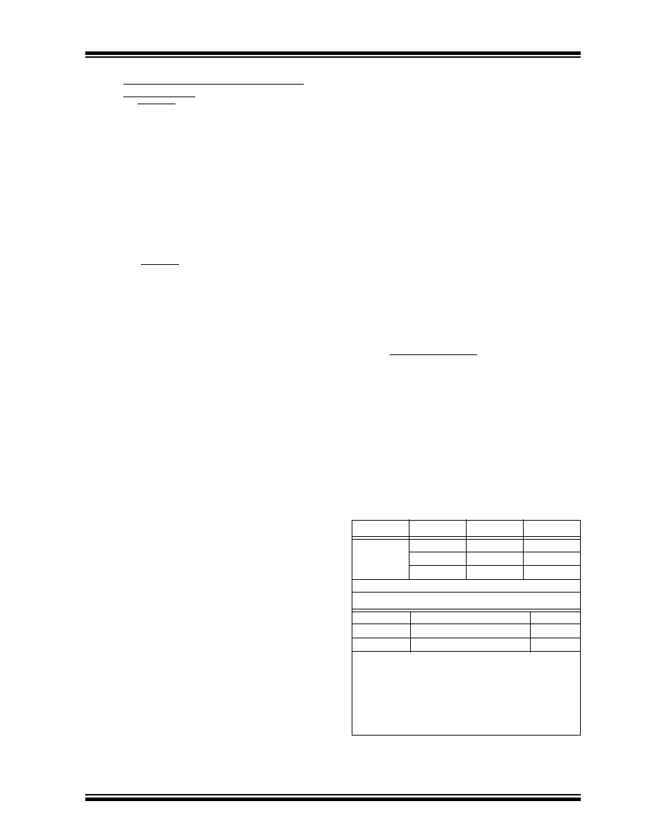
©
1997 Microchip Technology Inc.
DS30444E - page 53
PIC16C9XX
8.3
Timer1 Operation in Asynchronous
Counter Mode
If control bit T1SYNC (T1CON<2>) is set, the external
clock input is not synchronized. The timer continues to
increment asynchronous to the internal phase clocks.
The timer will continue to run during SLEEP and can
generate an interrupt on overflow which will wake-up
the processor. However, special precautions in soft-
ware are needed to read-from or write-to the Timer1
register pair (TMR1H:TMR1L) (Section 8.3.2).
In asynchronous counter mode, Timer1 cannot be used
as a time-base for capture or compare operations.
8.3.1
EXTERNAL CLOCK INPUT TIMING WITH
UNSYNCHRONIZED CLOCK
If control bit T1SYNC is set, the timer will increment
completely asynchronously. The input clock must meet
certain minimum high time and low time requirements,
as specified in timing parameters 45, 46, and 47.
8.3.2
READING AND WRITING TMR1 IN
ASYNCHRONOUS COUNTER MODE
Reading TMR1H or TMR1L while the timer is running,
from an external asynchronous clock, will ensure a
valid read (taken care of in hardware). However, the
user should keep in mind that reading the 16-bit timer
in two 8-bit values itself poses certain problems since
the timer may overflow between the reads.
For writes, it is recommended that the user simply stop
the timer and write the desired values. A write conten-
tion may occur by writing to the timer registers while the
register is incrementing. This may produce an unpre-
dictable value in the timer register.
Reading the 16-bit value requires some care.
Example
8-1 is an example routine to read the 16-bit
timer value. This is useful if the timer cannot be
stopped.
EXAMPLE 8-1:
READING A 16-BIT
FREE-RUNNING TIMER
; All interrupts are disabled
MOVF TMR1H, W ;Read high byte
MOVWF TMPH ;
MOVF TMR1L, W ;Read low byte
MOVWF TMPL ;
MOVF TMR1H, W ;Read high byte
SUBWF TMPH, W ;Sub 1st read
; with 2nd read
BTFSC STATUS,Z ;Is result = 0
GOTO CONTINUE ;Good 16-bit read
;
; TMR1L may have rolled over between the read
; of the high and low bytes. Reading the high
; and low bytes now will read a good value.
;
MOVF TMR1H, W ;Read high byte
MOVWF TMPH ;
MOVF TMR1L, W ;Read low byte
MOVWF TMPL ;
; Re-enable the Interrupt (if required)
CONTINUE ;Continue with your code
8.4
Timer1 Oscillator
A crystal oscillator circuit is built in between pins T1OSI
(input) and T1OSO (amplifier output). It is enabled by
setting control bit T1OSCEN (T1CON<3>). The oscilla-
tor is a low power oscillator rated up to 200 kHz. It will
continue to run during SLEEP. It is primarily intended
for a 32 kHz crystal. Table 8-1 shows the capacitor
selection for the Timer1 oscillator.
The Timer1 oscillator is identical to the LP oscillator.
The user must provide a software time delay to ensure
proper oscillator start-up.
TABLE 8-1: CAPACITOR SELECTION FOR
THE TIMER1 OSCILLATOR
Osc Type
Freq
C1
C2
LP
32 kHz
33 pF
33 pF
100 kHz
15 pF
15 pF
200 kHz
15 pF
15 pF
These values are for design guidance only.
Crystals Tested:
32.768 kHz
Epson C-001R32.768K-A
±
20 PPM
100 kHz
Epson C-2 100.00 KC-P
±
20 PPM
200 kHz
STD XTL 200.000 kHz
±
20 PPM
Note 1: Higher capacitance increases the stability
of oscillator but also increases the start-up
time.
2: Since each resonator/crystal has its own
characteristics, the user should consult the
resonator/crystal manufacturer for appropri-
ate values of external components.
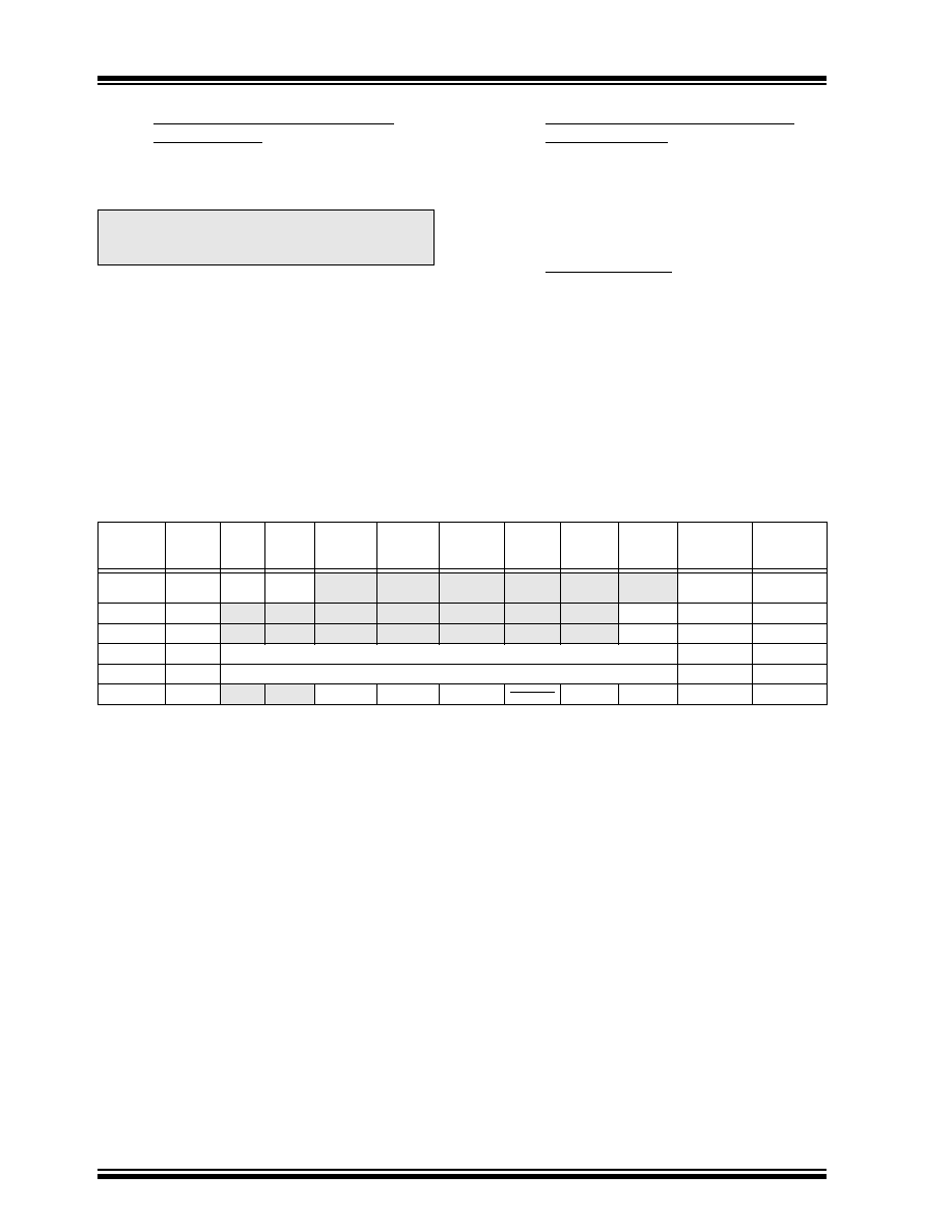
PIC16C9XX
DS30444E - page 54
©
1997 Microchip Technology Inc.
8.5
Resetting Timer1 using the CCP
Trigger Output
If the CCP1 module is configured in compare mode to
generate a "special event trigger" (CCP1M3:CCP1M0
=
1011
), this signal will reset Timer1.
Timer1 must be configured for either timer or synchro-
nized counter mode to take advantage of this feature. If
Timer1 is running in asynchronous counter mode, this
reset operation may not work.
In the event that a write to Timer1 coincides with a spe-
cial event trigger from CCP1, the write will take prece-
dence.
In this mode of operation, the CCPR1H:CCPR1L regis-
ters pair effectively becomes the period register for
Timer1.
Note:
The special event trigger from the CCP1
module will not set interrupt flag bit
TMR1IF (PIR1<0>).
8.6
Resetting of Timer1 Register Pair
(TMR1H:TMR1L)
TMR1H and TMR1L registers are not reset on a POR
or any other reset except by the CCP1 special event
trigger.
T1CON register is reset to 00h on a Power-on Reset. In
any other reset, the register is unaffected.
8.7
Timer1 Prescaler
The prescaler counter is cleared on writes to the
TMR1H or TMR1L registers.
TABLE 8-2: REGISTERS ASSOCIATED WITH TIMER1 AS A TIMER/COUNTER
Address
Name
Bit 7
Bit 6
Bit 5
Bit 4
Bit 3
Bit 2
Bit 1
Bit 0
Value on
Power-on
Reset
Value on
all other
resets
0Bh, 8Bh,
10Bh, 18Bh
INTCON
GIE
PEIE
T0IE
INTE
RBIE
T0IF
INTF
RBIF
0000 000x
0000 000u
0Ch
PIR1
LCDIF
ADIF
(1)
--
--
SSPIF
CCP1IF
TMR2IF
TMR1IF
00-- 0000
00-- 0000
8Ch
PIE1
LCDIE
ADIE
(1)
--
--
SSPIE
CCP1IE
TMR2IE
TMR1IE
00-- 0000
00-- 0000
0Eh
TMR1L
Holding register for the Least Significant Byte of the 16-bit TMR1 register
xxxx xxxx
uuuu uuuu
0Fh
TMR1H
Holding register for the Most Significant Byte of the 16-bit TMR1 register
xxxx xxxx
uuuu uuuu
10h
T1CON
--
--
T1CKPS1
T1CKPS0
T1OSCEN
T1SYNC
TMR1CS
TMR1ON
--00 0000
--uu uuuu
Legend:
x
= unknown,
u
= unchanged,
-
= unimplemented read as '0'. Shaded cells are not used by theTimer1 module.
Note
1: Bits ADIE and ADIF are reserved on the PIC16C923, always maintain these bits clear.
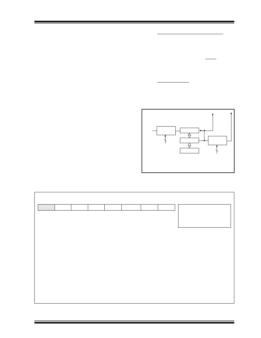
©
1997 Microchip Technology Inc.
DS30444E - page 55
PIC16C9XX
9.0
TIMER2 MODULE
Timer2 is an 8-bit timer with a prescaler and a
postscaler. It can be used as the PWM time-base for
the PWM mode of the CCP module. The TMR2 register
is readable and writable, and is cleared on any device
reset.
The input clock (F
OSC
/4) has a prescale option of 1:1,
1:4 or 1:16 (selected by control bits
T2CKPS1:T2CKPS0 (T2CON<1:0>)).
The Timer2 module has an 8-bit period register, PR2.
TMR2 increments from 00h until it matches PR2 and
then resets to 00h on the next increment cycle. PR2 is
a readable and writable register. The PR2 register is set
during RESET.
The match output of TMR2 goes through a 4-bit
postscaler (which gives a 1:1 to 1:16 scaling inclusive)
to generate a TMR2 interrupt (latched in flag bit
TMR2IF, (PIR1<1>)).
Timer2 can be shut off by clearing control bit TMR2ON
(T2CON<2>) to minimize power consumption.
Figure 9-2 shows the Timer2 control register.
9.1
Timer2 Prescaler and Postscaler
The prescaler and postscaler counters are cleared
when any of the following occurs:
· a write to the TMR2 register
· a write to the T2CON register
· any device reset (Power-on Reset, MCLR Reset,
or Watchdog Timer Reset)
TMR2 will not clear when T2CON is written.
9.2
Output of TMR2
The output of TMR2 (before the postscaler) is fed to the
Synchronous Serial Port module which optionally uses
it to generate shift clock.
FIGURE 9-1:
TIMER2 BLOCK DIAGRAM
Comparator
TMR2
Sets flag
TMR2 reg
output
(1)
Reset
Postscaler
Prescaler
PR2 reg
2
Fosc/4
1:1
1:16
1:1, 1:4, 1:16
EQ
4
bit TMR2IF
Note
1: TMR2 register output can be software selected
by the SSP Module as the source clock.
to
FIGURE 9-2:
T2CON: TIMER2 CONTROL REGISTER (ADDRESS 12h)
U-0
R/W-0
R/W-0
R/W-0
R/W-0
R/W-0
R/W-0
R/W-0
--
TOUTPS3 TOUTPS2 TOUTPS1 TOUTPS0 TMR2ON
T2CKPS1 T2CKPS0
R
= Readable bit
W = Writable bit
U
= Unimplemented bit,
read as `0'
- n = Value at POR reset
bit7
bit0
bit 7:
Unimplemented: Read as '0'
bit 6-3:
TOUTPS3:TOUTPS0: Timer2 Output Postscale Select bits
0000
= 1:1 Postscale
0001
= 1:2 Postscale
·
·
·
1111
= 1:16 Postscale
bit 2:
TMR2ON: Timer2 On bit
1 = Timer2 is on
0 = Timer2 is off
bit 1-0:
T2CKPS1:T2CKPS0: Timer2 Clock Prescale Select bits
00
= Prescaler is 1
01
= Prescaler is 4
1x
= Prescaler is 16
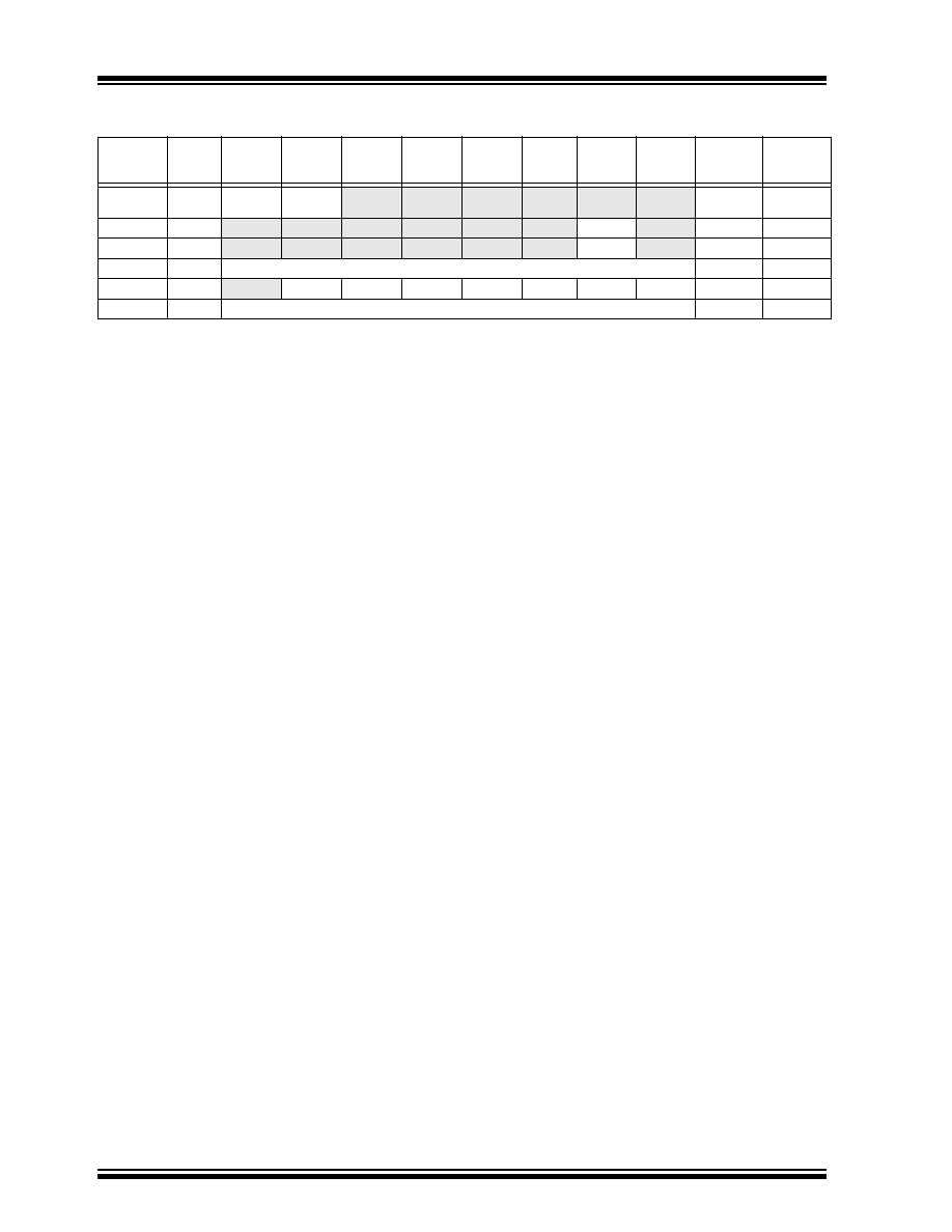
PIC16C9XX
DS30444E - page 56
©
1997 Microchip Technology Inc.
TABLE 9-1: REGISTERS ASSOCIATED WITH TIMER2 AS A TIMER/COUNTER
Address
Name
Bit 7
Bit 6
Bit 5
Bit 4
Bit 3
Bit 2
Bit 1
Bit 0
Value on
Power-on
Reset
Value on
all other
resets
0Bh, 8Bh,
10Bh, 18Bh
INTCON
GIE
PEIE
T0IE
INTE
RBIE
T0IF
INTF
RBIF
0000 000x
0000 000u
0Ch
PIR1
LCDIF
ADIF
(1)
--
--
SSPIF
CCP1IF
TMR2IF
TMR1IF
00-- 0000
00-- 0000
8Ch
PIE1
LCDIE
ADIE
(1)
--
--
SSPIE
CCP1IE
TMR2IE
TMR1IE
00-- 0000
00-- 0000
11h
TMR2
Timer2 module's register
0000 0000
0000 0000
12h
T2CON
--
TOUTPS3
TOUTPS2
TOUTPS1
TOUTPS0 TMR2ON T2CKPS1
T2CKPS0
-000 0000
-000 0000
92h
PR2
Timer2 Period Register
1111 1111
1111 1111
Legend:
x
= unknown,
u
= unchanged,
-
= unimplemented read as '0'. Shaded cells are not used by the Timer2 module.
Note
1: Bits ADIE and ADIF are reserved on the PIC16C923, always maintain these bits clear.

©
1997 Microchip Technology Inc.
DS30444E - page 57
PIC16C9XX
10.0
CAPTURE/COMPARE/PWM
(CCP) MODULE
The CCP (Capture/Compare/PWM) module contains a
16-bit register which can operate as a 16-bit capture
register, as a 16-bit compare register, or as a PWM
master/slave duty cycle register. Table 10-1 shows the
timer resources used by the CCP module.
Capture/Compare/PWM Register1 (CCPR1) is com-
prised of two 8-bit registers: CCPR1L (low byte) and
CCPR1H (high byte). The CCP1CON register controls
the operation of CCP1. All three are readable and writ-
able.
Figure 10-1 shows the CCP1CON register.
For use of the CCP module, refer to the
Embedded
Control Handbook, "Using the CCP Modules" (AN594).
TABLE 10-1: CCP MODE - TIMER RESOURCE
CCP Mode
Timer Resource
Capture
Compare
PWM
Timer1
Timer1
Timer2
FIGURE 10-1: CCP1CON REGISTER (ADDRESS 17h)
U-0
U-0
R/W-0
R/W-0
R/W-0
R/W-0
R/W-0
R/W-0
--
--
CCP1X
CCP1Y CCP1M3
CCP1M2
CCP1M1 CCP1M0
R = Readable bit
W = Writable bit
U = Unimplemented bit,
read as `0'
- n =Value at POR reset
bit7
bit0
bit 7-6:
Unimplemented: Read as '0'
bit 5-4: CCP1X:CCP1Y: PWM Least Significant bits
Capture Mode
Unused
Compare Mode
Unused
PWM Mode
These bits are the two LSbs of the PWM duty cycle. The eight MSbs are found in CCPR1L.
bit 3-0: CCP1M3:CCP1M0: CCP1 Mode Select bits
0000
= Capture/Compare/PWM off (resets CCP1 module)
0100
= Capture mode, every falling edge
0101
= Capture mode, every rising edge
0110
= Capture mode, every 4th rising edge
0111
= Capture mode, every 16th rising edge
1000
= Compare mode, set output on match (bit CCP1IF is set)
1001
= Compare mode, clear output on match (bit CCP1IF is set)
1010
= Compare mode, generate software interrupt on match (bit CCP1IF is set, CCP1 pin is unaffected)
1011
= Compare mode, trigger special event (CCP1IF bit is set; CCP1 resets TMR1)
11xx
= PWM mode
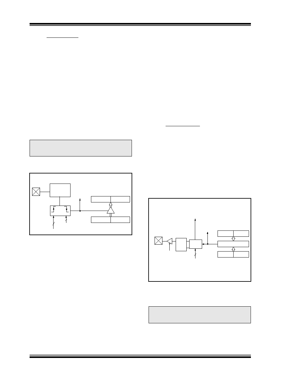
PIC16C9XX
DS30444E - page 58
©
1997 Microchip Technology Inc.
10.1
Capture Mode
In Capture mode, CCPR1H:CCPR1L captures the
16-bit value of the TMR1 register when an event occurs
on pin RC2/CCP1 (Figure 10-2). An event is defined as:
· Every falling edge
· Every rising edge
· Every 4th rising edge
· Every 16th rising edge
An event is selected by control bits CCP1M3:CCP1M0
(CCP1CON<3:0>). When a capture is made, the inter-
rupt request flag bit CCP1IF (PIR1<2>) is set. It must
be cleared in software. If another capture occurs before
the value in register CCPR1 is read, the old captured
value will be lost.
10.1.1
CCP PIN CONFIGURATION
In capture mode, the RC2/CCP1 pin should be config-
ured as an input by setting the TRISC<2> bit.
FIGURE 10-2: CAPTURE MODE OPERATION
BLOCK DIAGRAM
10.1.2
TIMER1 MODE SELECTION
Timer1 must be running in timer mode or synchronized
counter mode for the CCP module to use the capture
feature. In asynchronous counter mode the capture
operation may not work.
10.1.3
SOFTWARE INTERRUPT
When the Capture mode is changed, a false capture
interrupt may be generated. The user should keep
enable bit CCP1IE (PIE1<2>) clear to avoid false inter-
rupts and should clear flag bit CCP1IF following any
such change in operating mode.
10.1.4
CCP PRESCALER
There are four prescaler settings, specified by bits
CCP1M3:CCP1M0. Whenever the CCP module is
turned off, or the CCP module is not in Capture mode,
the prescaler counter is cleared. This means that any
reset will clear the prescaler counter.
Note:
If the RC2/CCP1 pin is configured as an
output, a write to the port can cause a cap-
ture condition.
CCPR1H
CCPR1L
TMR1H
TMR1L
Set CCP1IF
PIR1<2>
Capture
Enable
Q's
CCP1CON<3:0>
RC2/CCP1
Prescaler
÷
1, 4, 16
and
edge detect
pin
CCP
Switching from one capture prescaler to another may
generate an interrupt. Also, the prescaler counter will
not be cleared, therefore the first capture may be from
a non-zero prescaler. Example 10-1 shows the recom-
mended method for switching between capture prescal-
ers. This example also clears the prescaler counter and
will not generate the "false" interrupt.
EXAMPLE 10-1: CHANGING BETWEEN
CAPTURE PRESCALERS
CLRF CCP1CON
; Turn CCP module off
MOVLW NEW_CAPT_PS ; Load the W reg with
; the new prescaler
; mode value and CCP ON
MOVWF CCP1CON
; Load CCP1CON with
; this value
10.2
Compare Mode
In Compare mode, the 16-bit CCPR1 register value is
constantly compared against the TMR1 register pair
value. When a match occurs, the RC2/CCP1 pin is:
· Driven High
· Driven Low
· Remains Unchanged
The action on the pin is based on the value of control
bits CCP1M3:CCP1M0 (CCP1CON<3:0>). At the
same time, a compare interrupt is also generated.
FIGURE 10-3: COMPARE MODE
OPERATION BLOCK DIAGRAM
10.2.1
CCP PIN CONFIGURATION
The user must configure the RC2/CCP1 pin as an out-
put by clearing the TRISC<2> bit.
Note:
Clearing the CCP1CON register will force
the RC2/CCP1 compare output latch to the
default low level. This is not the data latch.
CCPR1H CCPR1L
TMR1H
TMR1L
Comparator
Q
S
R
Output
Logic
Special event trigger will reset Timer1, but not
T
r
igger
Set CCP1IF
PIR1<2>
match
RC2/CCP1
TRISC<2>
CCP1CON<3:0>
Mode Select
Output Enable
set interrupt flag bit TMR1IF (PIR1<0>).
©
1997 Microchip Technology Inc.
DS30444E - page 59
PIC16C9XX
10.2.1
TIMER1 MODE SELECTION
Timer1 must be running in Timer mode or Synchro-
nized Counter mode if the CCP module is using the
compare feature. In Asynchronous Counter mode, the
compare operation may not work.
10.2.2
SOFTWARE INTERRUPT MODE
When Generate Software Interrupt is chosen, the
CCP1 pin is not affected. Only a CCP interrupt is gen-
erated (if enabled).
10.2.3
SPECIAL EVENT TRIGGER
In this mode, an internal hardware trigger is generated
which may be used to initiate an action.
The special event trigger output of CCP1 resets the
TMR1 register pair and starts an A/D conversion. This
allows the CCPR1H:CCPR1L register pair to effectively
be a 16-bit programmable period register for Timer1.
10.3
PWM Mode
In Pulse Width Modulation (PWM) mode, the CCP1 pin
produces up to a 10-bit resolution PWM output. Since
the CCP1 pin is multiplexed with the PORTC data latch,
the TRISC<2> bit must be cleared to make the CCP1
pin an output.
Figure 10-4 shows a simplified block diagram of the
CCP module in PWM mode.
For a step by step procedure on how to set up the CCP
module for PWM operation, see Section 10.3.3.
Note:
The "special event trigger" from the CCP1
module will not set interrupt flag bit
TMR1IF (PIR1<0>).
Note:
Clearing the CCP1CON register will force
the CCP1 PWM output latch to the default
low level. This is not the PORTC I/O data
latch.
FIGURE 10-4: SIMPLIFIED PWM BLOCK
DIAGRAM
A PWM output (Figure 10-5) has a time-base (period)
and a time that the output stays high (duty cycle). The
frequency of the PWM is the inverse of the period
(1/period).
FIGURE 10-5: PWM OUTPUT
10.3.1
PWM PERIOD
The PWM period is specified by writing to the PR2 reg-
ister. The PWM period can be calculated using the fol-
lowing formula:
PWM period = [ (PR2) + 1 ] · 4 · T
OSC
·
(TMR2 prescale value)
PWM frequency is defined as 1 / [PWM period].
When TMR2 is equal to PR2, the following three events
occur on the next increment cycle:
· TMR2 is cleared
· The CCP1 pin is set (exception: if PWM duty
cycle = 0%, the CCP1 pin will not be set)
· The PWM duty cycle is latched from CCPR1L into
CCPR1H
CCPR1L
CCPR1H (Slave)
Comparator
TMR2
Comparator
PR2
(Note 1)
R
Q
S
Duty cycle registers
CCP1CON<5:4>
Clear Timer,
CCP1 pin and
latch D.C.
TRISC<2>
RC1/CCP1
Note 1: 8-bit timer is concatenated with 2-bit internal Q clock
or 2 bits of the prescaler to create 10-bit time-base.
Period
Duty Cycle
TMR2 = PR2
TMR2 = Duty Cycle
TMR2 = PR2
PIC16C9XX
DS30444E - page 60
©
1997 Microchip Technology Inc.
10.3.2
PWM DUTY CYCLE
The PWM duty cycle is specified by writing to the
CCPR1L register and to the CCP1CON<5:4> bits. Up
to 10-bit resolution is available: the CCPR1L contains
the eight MSbs and CCP1CON<5:4> contains the two
LSbs.
This 10-bit value is represented by
CCPR1L:CCP1CON<5:4>.
The following equation is
used to calculate the PWM duty cycle in time:
PWM duty cycle = (CCPR1L:CCP1CON<5:4>) ·
Tosc · (TMR2 prescale value)
CCPR1L and CCP1CON<5:4> can be written to at any
time, but the duty cycle value is not latched into
CCPR1H until after a match between PR2 and TMR2
occurs (i.e., the period is complete). In PWM mode,
CCPR1H is a read-only register.
The CCPR1H register and a 2-bit internal latch are
used to double buffer the PWM duty cycle. This double
buffering is essential for glitchless PWM operation.
When the CCPR1H and 2-bit latch match TMR2 con-
catenated with an internal 2-bit Q clock or 2 bits of the
TMR2 prescaler, the CCP1 pin is cleared.
Maximum PWM resolution (bits) for a given PWM fre-
quency:
Note:
The Timer2 postscaler (Section 9.0) is not
used in the determination of the PWM fre-
quency. The postscaler could be used to
have a servo update rate at a different fre-
quency than the PWM output.
Note:
If the PWM duty cycle value is longer than
the PWM period the CCP1 pin will not be
cleared.
log
(
F
PWM
log(2)
F
OSC
)
bits
=
EXAMPLE 10-2: PWM PERIOD AND DUTY
CYCLE CALCULATION
Desired PWM frequency is 31.25 kHz,
Fosc = 8 MHz
TMR2 prescale = 1
1/31.25 kHz
= [ (PR2) + 1 ] · 4 · 1/8 MHz · 1
32
µ
s
= [ (PR2) + 1 ] · 4 · 125 ns · 1
PR2
= 63
Find the maximum resolution of the duty cycle that can
be used with a 31.25 kHz frequency and 8 MHz oscilla-
tor:
1/31.25 kHz
= 2
PWM
RESOLUTION
· 1/8 MHz · 1
32
µ
s
= 2
PWM
RESOLUTION
· 125 ns · 1
256
= 2
PWM
RESOLUTION
log(256)
= (PWM Resolution) · log(2)
8.0
= PWM Resolution
At most, an 8-bit resolution duty cycle can be obtained
from a 31.25 kHz frequency and a 8 MHz oscillator, i.e.,
0
CCPR1L:CCP1CON<5:4>
255. Any value greater
than 255 will result in a 100% duty cycle.
In order to achieve higher resolution, the PWM fre-
quency must be decreased. In order to achieve higher
PWM frequency, the resolution must be decreased.
Table 10-2 lists example PWM frequencies and resolu-
tions for Fosc = 8 MHz. TMR2 prescaler and PR2 val-
ues are also shown.
10.3.3
SET-UP FOR PWM OPERATION
The following steps should be taken when configuring
the CCP module for PWM operation:
1.
Set the PWM period by writing to the PR2 regis-
ter.
2.
Set the PWM duty cycle by writing to the
CCPR1L register and CCP1CON<5:4> bits.
3.
Make the CCP1 pin an output by clearing the
TRISC<2> bit.
4.
Set the TMR2 prescale value and enable Timer2
by writing to T2CON.
5.
Configure the CCP module for PWM operation.
TABLE 10-2: EXAMPLE PWM FREQUENCIES AND RESOLUTIONS AT 8 MHz
PWM Frequency
488 Hz
1.95 kHz
7.81 kHz
31.25 kHz
62.5 kHz
250 kHz
Timer Prescaler (1, 4, 16)
16
4
1
1
1
1
PR2 Value
0xFF
0xFF
0xFF
0x3F
0x1F
0x07
Maximum Resolution (bits)
10
10
10
8
7
5
©
1997 Microchip Technology Inc.
DS30444E - page 61
PIC16C9XX
TABLE 10-3: REGISTERS ASSOCIATED WITH TIMER1, CAPTURE AND COMPARE
TABLE 10-4: REGISTERS ASSOCIATED WITH PWM AND TIMER2
Address
Name
Bit 7
Bit 6
Bit 5
Bit 4
Bit 3
Bit 2
Bit 1
Bit 0
Value on
Power-on
Reset
Value on
all other
Resets
0Bh, 8Bh,
10Bh, 18Bh
INTCON
GIE
PEIE
T0IE
INTE
RBIE
T0IF
INTF
RBIF
0000 000x
0000 000u
0Ch
PIR1
LCDIF
ADIF
(1)
--
--
SSPIF
CCP1IF
TMR2IF
TMR1IF
00-- 0000
00-- 0000
8Ch
PIE1
LCDIE
ADIE
(1)
--
--
SSPIE
CCP1IE
TMR2IE
TMR1IE
00-- 0000
00-- 0000
87h
TRISC
--
--
PORTC Data Direction Control Register
--11 1111
--11 1111
0Eh
TMR1L
Holding register for the Least Significant Byte of the 16-bit TMR1 register
xxxx xxxx
uuuu uuuu
0Fh
TMR1H
Holding register for the Most Significant Byte of the 16-bit TMR1 register
xxxx xxxx
uuuu uuuu
10h
T1CON
--
--
T1CKPS1
T1CKPS0
T1OSCEN
T1SYNC
TMR1CS
TMR1ON
--00 0000
--uu uuuu
15h
CCPR1L
Capture/Compare/PWM1 (LSB)
xxxx xxxx
uuuu uuuu
16h
CCPR1H
Capture/Compare/PWM1 (MSB)
xxxx xxxx
uuuu uuuu
17h
CCP1CON
--
--
CCP1X
CCP1Y
CCP1M3
CCP1M2
CCP1M1
CCP1M0
--00 0000
--00 0000
Legend:
x
= unknown,
u
= unchanged,
-
= unimplemented locations read as '0'. Shaded cells are not used in these modes.
Note
1: Bits ADIE and ADIF reserved on the PIC16C923, always maintain these bits clear.
Address
Name
Bit 7
Bit 6
Bit 5
Bit 4
Bit 3
Bit 2
Bit 1
Bit 0
Value on
Power-on
Reset
Value on
all other
Resets
0Bh, 8Bh,
10Bh, 18Bh
INTCON
GIE
PEIE
T0IE
INTE
RBIE
T0IF
INTF
RBIF
0000 000x
0000 000u
0Ch
PIR1
LCDIF
ADIF
(1)
--
--
SSPIF
CCP1IF
TMR2IF
TMR1IF
00-- 0000
00-- 0000
8Ch
PIE1
LCDIE
ADIE
(1)
--
--
SSPIE
CCP1IE
TMR2IE
TMR1IE
00-- 0000
00-- 0000
87h
TRISC
--
--
PORTC Data Direction Control Register
--11 1111
--11 1111
11h
TMR2
Timer2 module's register
0000 0000
0000 0000
92h
PR2
Timer2 module's Period register
1111 1111
1111 1111
12h
T2CON
--
TOUTPS3
TOUTPS2
TOUTPS1
TOUTPS0
TMR2ON T2CKPS1
T2CKPS0
-000 0000
-000 0000
15h
CCPR1L
Capture/Compare/PWM1 (LSB)
xxxx xxxx
uuuu uuuu
16h
CCPR1H
Capture/Compare/PWM1 (MSB)
xxxx xxxx
uuuu uuuu
17h
CCP1CON
--
--
CCP1X
CCP1Y
CCP1M3
CCP1M2
CCP1M1
CCP1M0
--00 0000
--00 0000
Legend:
x
= unknown,
u
= unchanged,
-
= unimplemented locations read as '0'. Shaded cells are not used in this mode.
Note
1: Bits ADIE and ADIF reserved on the PIC16C923, always maintain these bits clear.

PIC16C9XX
DS30444E - page 62
©
1997 Microchip Technology Inc.
NOTES:
©
1997 Microchip Technology Inc.
DS30444E - page 63
PIC16C9XX
11.0
SYNCHRONOUS SERIAL
PORT (SSP) MODULE
The Synchronous Serial Port (SSP) module is a serial
interface useful for communicating with other periph-
eral or microcontroller devices. These peripheral
devices may be serial EEPROMs, shift registers, dis-
play drivers, A/D converters, etc. The SSP module can
operate in one of two modes:
· Serial Peripheral Interface (SPI)
· Inter-Integrated Circuit (I
2
C)
Refer to Application Note AN578,
"Use of the SSP
Module in the I
2
C Multi-Master Environment."
FIGURE 11-1: SSPSTAT: SYNC SERIAL PORT STATUS REGISTER
(ADDRESS 94h)
R/W-0 R/W-0
R-0
R-0
R-0
R-0
R-0
R-0
SMP
CKE
D/A
P
S
R/W
UA
BF
R = Readable bit
W = Writable bit
U = Unimplemented bit,
read as `0'
- n =Value at POR reset
bit7
bit0
bit 7:
SMP: SPI data input sample phase
SPI Master Mode
1 = Input data sampled at end of data output time
0 = Input data sampled at middle of data output time
SPI Slave Mode
SMP must be cleared when SPI is used in slave mode
bit 6:
CKE: SPI Clock Edge Select (Figure 11-5, Figure 11-6, and Figure 11-7)
CKP = 0
1 = Data transmitted on rising edge of SCK
0 = Data transmitted on falling edge of SCK
CKP = 1
1 = Data transmitted on falling edge of SCK
0 = Data transmitted on rising edge of SCK
bit 5:
D/A: Data/Address bit (I
2
C mode only)
1 = Indicates that the last byte received or transmitted was data
0 = Indicates that the last byte received or transmitted was address
bit 4:
P: Stop bit (I
2
C mode only. This bit is cleared when the SSP module is disabled, or when the Start bit was
detected last)
1 = Indicates that a stop bit has been detected last (this bit is '0' on RESET)
0 = Stop bit was not detected last
bit 3:
S: Start bit (I
2
C mode only. This bit is cleared when the SSP module is disabled, or when the Stop bit was
detected last)
1 = Indicates that a start bit has been detected last (this bit is '0' on RESET)
0 = Start bit was not detected last
bit 2:
R/W: Read/Write bit information (I
2
C mode only)
This bit holds the R/W bit information following the last address match. This bit is only valid from the
address match to the next start bit, stop bit, or ACK bit.
1 = Read
0 = Write
bit 1:
UA: Update Address (10-bit I
2
C mode only)
1 = Indicates that the user needs to update the address in the SSPADD register
0 = Address does not need to be updated
bit 0:
BF: Buffer Full Status bit
Receive (SPI and I
2
C modes)
1 = Receive complete, SSPBUF is full
0 = Receive not complete, SSPBUF is empty
Transmit (I
2
C mode only)
1 = Transmit in progress, SSPBUF is full
0 = Transmit complete, SSPBUF is empty

PIC16C9XX
DS30444E - page 64
©
1997 Microchip Technology Inc.
FIGURE 11-2: SSPCON: SYNC SERIAL PORT CONTROL REGISTER (ADDRESS 14h)
R/W-0
R/W-0
R/W-0
R/W-0
R/W-0
R/W-0
R/W-0
R/W-0
WCOL
SSPOV
SSPEN
CKP
SSPM3
SSPM2
SSPM1
SSPM0
R = Readable bit
W = Writable bit
U = Unimplemented bit,
read as `0'
- n =Value at POR reset
bit7
bit0
bit 7:
WCOL: Write Collision Detect bit
1 = The SSPBUF register is written while it is still transmitting the previous word
(must be cleared in software)
0 = No collision
bit 6:
SSPOV: Receive Overflow Indicator bit
In SPI mode
1 = A new byte is received while the SSPBUF register is still holding the previous data. In case of overflow,
the data in SSPSR is lost. Overflow can only occur in slave mode. The user must read the SSPBUF, even
if only transmitting data, to avoid setting overflow. In master mode the overflow bit is not set since each
new reception (and transmission) is initiated by writing to the SSPBUF register.
0 = No overflow
In I
2
C mode
1 = A byte is received while the SSPBUF register is still holding the previous byte. SSPOV is a "don't care"
in transmit mode. SSPOV must be cleared in software in either mode.
0 = No overflow
bit 5:
SSPEN: Synchronous Serial Port Enable bit
In SPI mode
1 = Enables serial port and configures SCK, SDO, and SDI as serial port pins
0 = Disables serial port and configures these pins as I/O port pins
In I
2
C mode
1 = Enables the serial port and configures the SDA and SCL pins as serial port pins
0 = Disables serial port and configures these pins as I/O port pins
In both modes, when enabled, these pins must be properly configured as input or output.
bit 4:
CKP: Clock Polarity Select bit
In SPI mode
1 = Idle state for clock is a high level
0 = Idle state for clock is a low level
In I
2
C mode
SCK release control
1 = Enable clock
0 = Holds clock low (clock stretch) (Used to ensure data setup time)
bit 3-0: SSPM3:SSPM0: Synchronous Serial Port Mode Select bits
0000
= SPI master mode, clock = F
OSC
/4
0001
= SPI master mode, clock = F
OSC
/16
0010
= SPI master mode, clock = F
OSC
/64
0011
= SPI master mode, clock = TMR2 output/2
0100
= SPI slave mode, clock = SCK pin. SS pin control enabled.
0101
= SPI slave mode, clock = SCK pin. SS pin control disabled. SS can be used as I/O pin
0110
= I
2
C slave mode, 7-bit address
0111
= I
2
C slave mode, 10-bit address
1011
= I
2
C Firmware controlled master mode (slave idle)
1110
= I
2
C slave mode, 7-bit address with start and stop bit interrupts enabled
1111
= I
2
C slave mode, 10-bit address with start and stop bit interrupts enabled
©
1997 Microchip Technology Inc.
DS30444E - page 65
PIC16C9XX
11.1
SPI Mode
The SPI mode allows 8-bits of data to be synchro-
nously transmitted and received simultaneously. To
accomplish communication, typically three pins are
used:
· Serial Data Out (SDO) RC5/SDO
· Serial Data In (SDI) RC4/SDI
· Serial Clock (SCK) RC3/SCK
Additionally a fourth pin may be used when in a slave
mode of operation:
· Slave Select (SS) RA5/AN4/SS (the AN4 function
is implemented on the PIC16C924 only)
When initializing the SPI, several options need to be
specified. This is done by programming the appropriate
control bits in the SSPCON register (SSPCON<5:0>)
and SSPSTAT<7:6>. These control bits allow the fol-
lowing to be specified:
· Master Mode (SCK is the clock output)
· Slave Mode (SCK is the clock input)
· Clock Polarity (Idle state of SCK)
· Clock edge (output data on rising/falling edge of
SCK)
· Clock Rate (Master mode only)
· Slave Select Mode (Slave mode only)
The SSP consists of a transmit/receive Shift Register
(SSPSR) and a buffer register (SSPBUF). The SSPSR
shifts the data in and out of the device, MSb first. The
SSPBUF holds the data that was written to the SSPSR,
until the received data is ready. Once the 8-bits of data
have been received, that byte is moved to the SSPBUF
register. Then the buffer full detect bit BF
(SSPSTAT<0>) and interrupt flag bit SSPIF (PIR1<3>)
are set. This double buffering of the received data
(SSPBUF) allows the next byte to start reception before
reading the data that was just received. Any write to the
SSPBUF register during transmission/reception of data
will be ignored, and the write collision detect bit WCOL
(SSPCON<7>) will be set. User software must clear the
WCOL bit so that it can be determined if the following
write(s) to the SSPBUF register completed success-
fully. When the application software is expecting to
receive valid data, the SSPBUF should be read before
the next byte of data to transfer is written to the
SSPBUF. Buffer full bit BF (SSPSTAT<0>) indicates
when SSPBUF has been loaded with the received data
(transmission is complete). When the SSPBUF is read,
bit BF is cleared. This data may be irrelevant if the SPI
is only a transmitter. Generally the SSP Interrupt is
used to determine when the transmission/reception
has completed. The SSPBUF must be read and/or writ-
ten. If the interrupt method is not going to be used, then
software polling can be done to ensure that a write col-
lision does not occur. Example 11-1 shows the loading
of the SSPBUF (SSPSR) for data transmission. The
shaded instruction is only required if the received data
is meaningful.
EXAMPLE 11-1: LOADING THE SSPBUF
(SSPSR) REGISTER
BCF STATUS, RP1 ;Select Bank1
BSF STATUS, RP0 ;
LOOP BTFSS SSPSTAT, BF ;Has data been
;received
;(transmit
;complete)?
GOTO LOOP ;No
BCF STATUS, RP0 ;Select Bank0
MOVF SSPBUF, W ;W reg = contents
; of SSPBUF
MOVF TXDATA, W ;W reg = contents
; of TXDATA
MOVWF SSPBUF ;New data to xmit
The block diagram of the SSP module, when in SPI
mode (Figure 11-3), shows that the SSPSR is not
directly readable or writable, and can only be accessed
from addressing the SSPBUF register. Additionally, the
SSP status register (SSPSTAT) indicates the various
status conditions.
FIGURE 11-3: SSP BLOCK DIAGRAM
(SPI MODE)
MOVWF RXDATA ;Save in user RAM
Read
Write
Internal
data bus
RC4/SDI/SDA
RC5/SDO
RA5/AN4/SS
RC3/SCK/
SSPSR reg
SSPBUF reg
SSPM3:SSPM0
bit0
shift
clock
SS Control
Enable
Edge
Select
Clock Select
TMR2 output
T
CY
Prescaler
4, 16, 64
TRISC<3>
2
Edge
Select
2
4
SCL
PIC16C9XX
DS30444E - page 66
©
1997 Microchip Technology Inc.
To enable the serial port, SSP Enable bit, SSPEN
(SSPCON<5>) must be set. To reset or reconfigure SPI
mode, clear bit SSPEN, re-initialize the SSPCON reg-
ister, and then set bit SSPEN. This configures the SDI,
SDO, SCK, and SS pins as serial port pins. For the pins
to behave as the serial port function, they must have
their data direction bits (in the TRISC register) appro-
priately programmed. That is:
· SDI must have TRISC<4> set
· SDO must have TRISC<5> cleared
· SCK (Master mode) must have TRISC<3>
cleared
· SCK (Slave mode) must have TRISC<3> set
· SS must have TRISA<5> set
Any serial port function that is not desired may be over-
ridden by programming the corresponding data direc-
tion (TRIS) register to the opposite value. An example
would be in master mode where you are only sending
data (to a display driver), then both SDI and SS could
be used as general purpose outputs by clearing their
corresponding TRIS register bits.
Figure 11-4 shows a typical connection between two
microcontrollers. The master controller (Processor 1)
initiates the data transfer by sending the SCK signal.
Data is shifted out of both shift registers on their pro-
grammed clock edge, and latched on the opposite edge
of the clock. Both processors should be programmed to
same Clock Polarity (CKP), then both controllers would
send and receive data at the same time. Whether the
data is meaningful (or dummy data) depends on the
application software. This leads to three scenarios for
data transmission:
· Master sends data
--
Slave sends dummy data
· Master sends data
--
Slave sends data
· Master sends dummy data
--
Slave sends data
The master can initiate the data transfer at any time
because it controls the SCK. The master determines
when the slave (Processor 2) is to broadcast data by
the firmware protocol.
In master mode the data is transmitted/received as
soon as the SSPBUF register is written to. If the SPI is
only going to receive, the SCK output could be disabled
(programmed as an input). The SSPSR register will
continue to shift in the signal present on the SDI pin at
the programmed clock rate. As each byte is received, it
will be loaded into the SSPBUF register as if a normal
received byte (interrupts and status bits appropriately
set). This could be useful in receiver applications as a
"line activity monitor" mode.
In slave mode, the data is transmitted and received as
the external clock pulses appear on SCK. When the last
bit is latched the interrupt flag bit SSPIF (PIR1<3>) is
set.
The clock polarity is selected by appropriately program-
ming bit CKP (SSPCON<4>). This then would give
waveforms for SPI communication as shown in
Figure
11-5, Figure
11-6, and Figure 11-7 where the
MSB is transmitted first. In master mode, the SPI clock
rate (bit rate) is user programmable to be one of the fol-
lowing:
· F
OSC
/4 (or T
CY
)
· F
OSC
/16 (or 4 · T
CY
)
· F
OSC
/64 (or 16 · T
CY
)
· Timer2 output/2
This allows a maximum bit clock frequency (at 8 MHz)
of 2 MHz. When in slave mode the external clock must
meet the minimum high and low times.
In sleep mode, the slave can transmit and receive data
and wake the device from sleep.
FIGURE 11-4: SPI MASTER/SLAVE CONNECTION
Serial Input Buffer
(SSPBUF)
Shift Register
(SSPSR)
MSb
LSb
SDO
SDI
PROCESSOR 1
SCK
SPI Master SSPM3:SSPM0 =
00xx
b
Serial Input Buffer
(SSPBUF)
Shift Register
(SSPSR)
LSb
MSb
SDI
SDO
PROCESSOR 2
SCK
SPI Slave SSPM3:SSPM0 =
010x
b
Serial Clock
©
1997 Microchip Technology Inc.
DS30444E - page 67
PIC16C9XX
The SS pin allows a synchronous slave mode. The
SPI must be in slave mode (SSPCON<3:0> = 04h)
and the TRISA<5> bit must be set for the synchro-
nous slave mode to be enabled. When the SS pin is
low, transmission and reception are enabled and the
SDO pin is driven. When the SS pin goes high, the
SDO pin is no longer driven, even if in the middle of
a transmitted byte, and becomes a floating output.
External pull-up/ pull-down resistors may be desirable,
depending on the application.
To emulate two-wire communication, the SDO pin can
be connected to the SDI pin. When the SPI needs to
operate as a receiver the SDO pin can be configured as
an input. This disables transmissions from the SDO.
The SDI can always be left as an input (SDI function)
since it cannot create a bus conflict.
Note:
When the SPI is in Slave Mode with SS pin
control enabled, (SSPCON<3:0> =
0100
)
the SPI module will reset if the SS pin is set
to V
DD
.
Note:
If the SPI is used in Slave Mode with
CKE = '1', then the SS pin control must be
enabled.
FIGURE 11-5: SPI MODE TIMING, MASTER MODE
FIGURE 11-6: SPI MODE TIMING (SLAVE MODE WITH CKE = 0)
SCK (CKP = 0,
SDI (SMP = 0)
SSPIF
bit7
bit6
bit5
bit4
bit3
bit2
bit1
bit0
SDI (SMP = 1)
SCK (CKP = 0,
SCK (CKP = 1,
SCK (CKP = 1,
SDO
bit7
bit7
bit0
bit0
CKE = 0)
CKE = 1)
CKE = 0)
CKE = 1)
SCK (CKP = 0)
SDI (SMP = 0)
SSPIF
bit7
bit6
bit5
bit4
bit3
bit2
bit1
bit0
SCK (CKP = 1)
SDO
bit7
bit0
SS (optional)
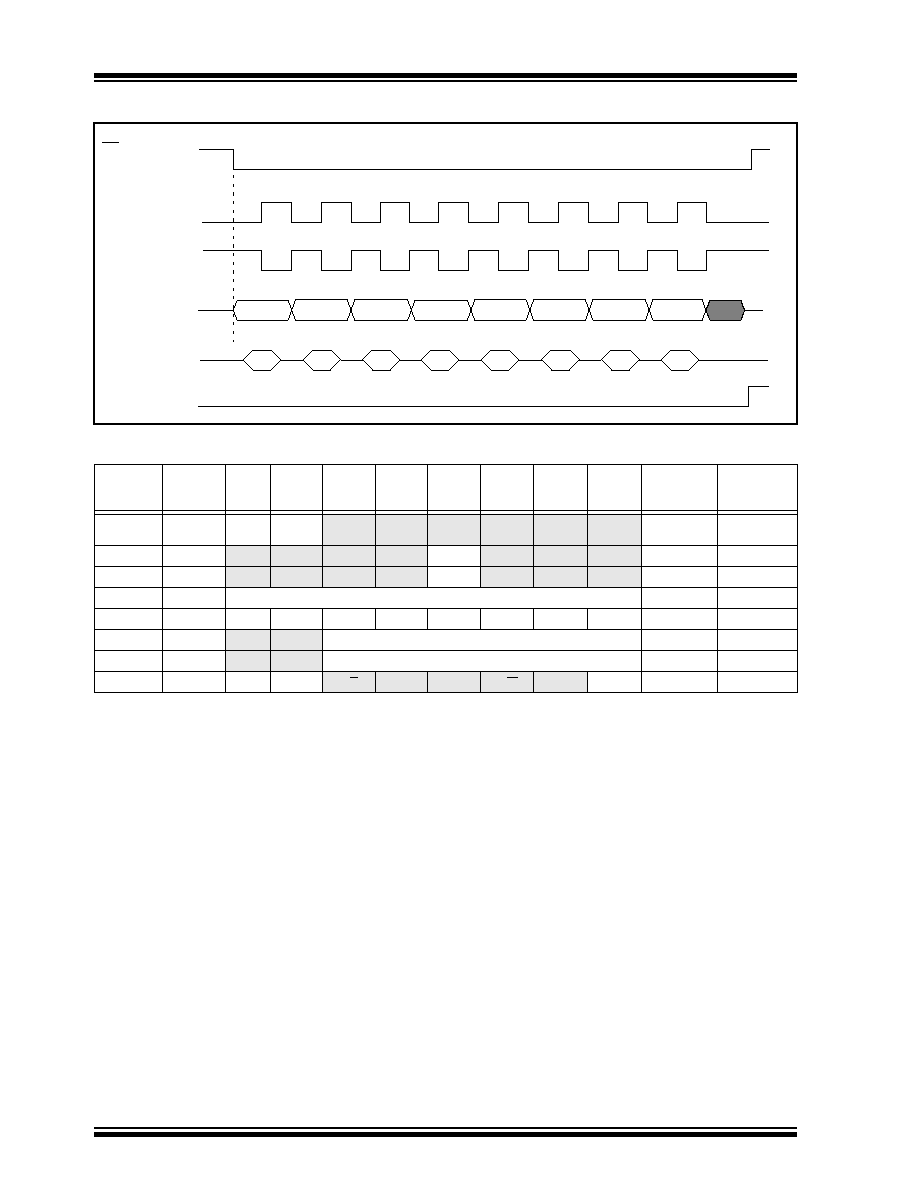
PIC16C9XX
DS30444E - page 68
©
1997 Microchip Technology Inc.
FIGURE 11-7: SPI MODE TIMING (SLAVE MODE WITH CKE = 1)
TABLE 11-1: REGISTERS ASSOCIATED WITH SPI OPERATION
Address
Name
Bit 7
Bit 6
Bit 5
Bit 4
Bit 3
Bit 2
Bit 1
Bit 0
Value on
Power-on
Reset
Value on all
other resets
0Bh, 8Bh,
10Bh, 18Bh
INTCON
GIE
PEIE
T0IE
INTE
RBIE
T0IF
INTF
RBIF
0000 000x
0000 000u
0Ch
PIR1
LCDIF
ADIF
(1)
--
--
SSPIF
CCP1IF
TMR2IF
TMR1IF
00-- 0000
00-- 0000
8Ch
PIE1
LCDIE
ADIE
(1)
--
--
SSPIE
CCP1IE
TMR2IE
TMR1IE
00-- 0000
00-- 0000
13h
SSPBUF
Synchronous Serial Port Receive Buffer/Transmit Register
xxxx xxxx
uuuu uuuu
14h
SSPCON
WCOL
SSPOV
SSPEN
CKP
SSPM3
SSPM2
SSPM1
SSPM0
0000 0000
0000 0000
85h
TRISA
--
--
PORTA Data Direction Control Register
--11 1111
--11 1111
87h
TRISC
--
--
PORTC Data Direction Control Register
--11 1111
--11 1111
94h
SSPSTAT
SMP
CKE
D/A
P
S
R/W
UA
BF
0000 0000
0000 0000
Legend:
x
= unknown,
u
= unchanged,
-
= unimplemented read as '0'. Shaded cells are not used by the SSP in SPI mode.
Note
1: Bits ADIE and ADIF are reserved on the PIC16C923, always maintain these bits clear.
SCK (CKP = 0)
SDI (SMP = 0)
SSPIF
bit7
bit6
bit5
bit4
bit3
bit2
bit1
bit0
SCK (CKP = 1)
SDO
bit7
bit0
SS
(not optional)
©
1997 Microchip Technology Inc.
DS30444E - page 69
PIC16C9XX
11.2
I
2
C
TM
Overview
This section provides an overview of the Inter-Inte-
grated Circuit (I
2
C) bus, with Section 11.3 discussing
the operation of the SSP module in I
2
C mode.
The I
2
C bus is a two-wire serial interface developed by
the Philips Corporation. The original specification, or
standard mode, was for data transfers of up to 100
Kbps. An enhanced specification, or fast mode is not
supported. This device will communicate with fast
mode devices if attached to the same bus.
The I
2
C interface employs a comprehensive protocol to
ensure reliable transmission and reception of data.
When transmitting data, one device is the "master"
which initiates transfer on the bus and generates the
clock signals to permit that transfer, while the other
device(s) acts as the "slave." All portions of the slave
protocol are implemented in the SSP module's hard-
ware, except general call support, while portions of the
master protocol need to be addressed in the
PIC16CXXX software. Table 11-2 defines some of the
I
2
C bus terminology. For additional information on the
I
2
C interface specification, refer to the Philips docu-
ment "
The I
2
C bus and how to use it." #939839340011,
which can be obtained from the Philips Corporation.
In the I
2
C interface protocol each device has an
address. When a master wishes to initiate a data trans-
fer, it first transmits the address of the device that it
wishes to "talk" to. All devices "listen" to see if this is
their address. Within this address, a bit specifies if the
master wishes to read-from/write-to the slave device.
The master and slave are always in opposite modes
(transmitter/receiver) of operation during a data trans-
fer. That is they can be thought of as operating in either
of these two relations:
· Master-transmitter and Slave-receiver
· Slave-transmitter and Master-receiver
In both cases the master generates the clock signal.
The output stages of the clock (SCL) and data (SDA)
lines must have an open-drain or open-collector in
order to perform the wired-AND function of the bus.
External pull-up resistors are used to ensure a high
level when no device is pulling the line down. The num-
ber of devices that may be attached to the I
2
C bus is
limited only by the maximum bus loading specification
of 400 pF.
11.2.1
INITIATING AND TERMINATING DATA
TRANSFER
During times of no data transfer (idle time), both the
clock line (SCL) and the data line (SDA) are pulled high
through the external pull-up resistors. The START and
STOP conditions determine the start and stop of data
transmission. The START condition is defined as a high
to low transition of the SDA when the SCL is high. The
STOP condition is defined as a low to high transition of
the SDA when the SCL is high. Figure 11-8 shows the
START and STOP conditions. The master generates
these conditions for starting and terminating data trans-
fer. Due to the definition of the START and STOP con-
ditions, when data is being transmitted, the SDA line
can only change state when the SCL line is low.
FIGURE 11-8: START AND STOP
CONDITIONS
SDA
SCL
S
P
Start
Condition
Change
of Data
Allowed
Change
of Data
Allowed
Stop
Condition
TABLE 11-2: I
2
C BUS TERMINOLOGY
Term
Description
Transmitter
The device that sends the data to the bus.
Receiver
The device that receives the data from the bus.
Master
The device which initiates the transfer, generates the clock and terminates the transfer.
Slave
The device addressed by a master.
Multi-master
More than one master device in a system. These masters can attempt to control the bus at the
same time without corrupting the message.
Arbitration
Procedure that ensures that only one of the master devices will control the bus. This ensure that
the transfer data does not get corrupted.
Synchronization
Procedure where the clock signals of two or more devices are synchronized.
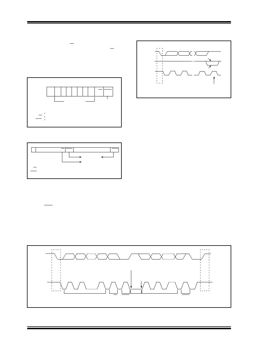
PIC16C9XX
DS30444E - page 70
©
1997 Microchip Technology Inc.
11.2.2
ADDRESSING I
2
C DEVICES
There are two address formats. The simplest is the 7-bit
address format with a R/W bit (Figure 11-9). The more
complex is the 10-bit address with a R/W bit
(Figure
11-10). For 10-bit address format, two bytes
must be transmitted with the first five bits specifying this
to be a 10-bit address.
FIGURE 11-9: 7-BIT ADDRESS FORMAT
FIGURE 11-10: I
2
C 10-BIT ADDRESS
FORMAT
11.2.3
TRANSFER ACKNOWLEDGE
All data must be transmitted per byte, with no limit to the
number of bytes transmitted per data transfer. After
each byte, the slave-receiver generates an acknowl-
edge bit (ACK) (Figure 11-11). When a slave-receiver
doesn't acknowledge the slave address or received
data, the master must abort the transfer. The slave
must leave SDA high so that the master can generate
the STOP condition (Figure 11-8).
S
R/W ACK
Sent by
Slave
slave address
S
R/W Read/Write pulse
MSb
LSb
Start Condition
ACK
Acknowledge
S 1 1 1 1 0 A9 A8 R/W ACK A7 A6 A5 A4 A3 A2 A1 A0 ACK
sent by slave
= 0 for write
S
R/W
ACK
- Start Condition
- Read/Write Pulse
- Acknowledge
FIGURE 11-11: SLAVE-RECEIVER
ACKNOWLEDGE
If the master is receiving the data (master-receiver), it
generates an acknowledge signal for each received
byte of data, except for the last byte. To signal the end
of data to the slave-transmitter, the master does not
generate an acknowledge (not acknowledge). The
slave then releases the SDA line so the master can
generate the STOP condition. The master can also
generate the STOP condition during the acknowledge
pulse for valid termination of data transfer.
If the slave needs to delay the transmission of the next
byte, holding the SCL line low will force the master into
a wait state. Data transfer continues when the slave
releases the SCL line. This allows the slave to move the
received data or fetch the data it needs to transfer
before allowing the clock to start. This wait state tech-
nique can also be implemented at the bit level,
Figure 11-12.
The slave will inherently stretch the clock,
when it is a transmitter, but will not when it is a receiver.
The slave will have to clear the SSPCON<4> bit to
enable clock stretching when it is a receiver.
S
Data
Output by
Transmitter
Data
Output by
Receiver
SCL from
Master
Start
Condition
Clock Pulse for
Acknowledgment
not acknowledge
acknowledge
1
2
8
9
FIGURE 11-12:
DATA TRANSFER WAIT STATE
1
2
7
8
9
1
2
3
·
8
9
P
SDA
SCL
S
Start
Condition
Address
R/W
ACK
Wait
State
Data
ACK
MSB
acknowledgment
signal from receiver
acknowledgment
signal from receiver
byte complete
interrupt with receiver
clock line held low while
interrupts are serviced
Stop
Condition
©
1997 Microchip Technology Inc.
DS30444E - page 71
PIC16C9XX
Figure 11-13 and Figure 11-14 show Master-transmit-
ter and Master-receiver data transfer sequences.
When a master does not wish to relinquish the bus (by
generating a STOP condition), a repeated START con-
dition (Sr) must be generated. This condition is identical
to the start condition (SDA goes high-to-low while SCL
is high), but occurs after a data transfer acknowledge
pulse (not the bus-free state). This allows a master to
send "commands" to the slave and then receive the
requested information or to address a different slave
device. This sequence is shown in Figure 11-15.
FIGURE 11-13: MASTER-TRANSMITTER SEQUENCE
FIGURE 11-14: MASTER-RECEIVER SEQUENCE
FIGURE 11-15: COMBINED FORMAT
For 7-bit address:
S
Slave Address
First 7 bits
S
R/W A1 Slave Address
Second byte
A2
Data A
Data
P
A master transmitter addresses a slave receiver
with a 10-bit address.
A/A
Slave Address R/W A Data A Data A/A P
'0' (write)
data transferred
(n bytes - acknowledge)
A master transmitter addresses a slave receiver with a
7-bit address. The transfer direction is not changed.
From master to slave
From slave to master
A = acknowledge (SDA low)
A = not acknowledge (SDA high)
S = Start Condition
P = Stop Condition
(write)
For 10-bit address:
For 7-bit address:
S
Slave Address
First 7 bits
S
R/W A1 Slave Address
Second byte
A2
A master transmitter addresses a slave receiver
with a 10-bit address.
Slave Address R/W A Data A Data A
P
'1' (read)
data transferred
(n bytes - acknowledge)
A master reads a slave immediately after the first byte.
From master to slave
From slave to master
A = acknowledge (SDA low)
A = not acknowledge (SDA high)
S = Start Condition
P = Stop Condition
(write)
For 10-bit address:
Slave Address
First 7 bits
Sr
R/W A3
A
Data A
P
Data
(read)
Combined format:
S
Combined format - A master addresses a slave with a 10-bit address, then transmits
Slave Address R/W A Data A/A Sr
P
(read)
Sr = repeated
Transfer direction of data and acknowledgment bits depends on R/W bits.
From master to slave
From slave to master
A = acknowledge (SDA low)
A = not acknowledge (SDA high)
S = Start Condition
P = Stop Condition
Slave Address
First 7 bits
Sr
R/W A
(write)
data to this slave and reads data from this slave.
Slave Address
Second byte
Data
Sr Slave Address
First 7 bits
R/W A Data A
A P
A
A
Data A/A
Data
(read)
Slave Address R/W A Data A/A
Start Condition
(write)
Direction of transfer
may change at this point
(read or write)
(n bytes + acknowledge)
PIC16C9XX
DS30444E - page 72
©
1997 Microchip Technology Inc.
11.2.4
MULTI-MASTER
The I
2
C protocol allows a system to have more than
one master. This is called multi-master. When two or
more masters try to transfer data at the same time, arbi-
tration and synchronization occur.
11.2.4.1
ARBITRATION
Arbitration takes place on the SDA line, while the SCL
line is high. The master which transmits a high when the
other master transmits a low loses arbitration
(Figure
11-16), and turns off its data output stage. A
master which lost arbitration can generate clock pulses
until the end of the data byte where it lost arbitration.
When the master devices are addressing the same
device, arbitration continues into the data.
FIGURE 11-16: MULTI-MASTER
ARBITRATION
(TWO MASTERS)
Masters that also incorporate the slave function, and
have lost arbitration must immediately switch over to
slave-receiver mode. This is because the winning mas-
ter-transmitter may be addressing it.
Arbitration is not allowed between:
· A repeated START condition
· A STOP condition and a data bit
· A repeated START condition and a STOP condi-
tion
Care needs to be taken to ensure that these conditions
do not occur.
transmitter 1 loses arbitration
DATA 1 SDA
DATA 1
DATA 2
SDA
SCL
11.2.4.2 Clock Synchronization
Clock synchronization occurs after the devices have
started arbitration. This is performed using a
wired-AND connection to the SCL line. A high to low
transition on the SCL line causes the concerned
devices to start counting off their low period. Once a
device clock has gone low, it will hold the SCL line low
until its SCL high state is reached. The low to high tran-
sition of this clock may not change the state of the SCL
line, if another device clock is still within its low period.
The SCL line is held low by the device with the longest
low period. Devices with shorter low periods enter a
high wait-state, until the SCL line comes high. When the
SCL line comes high, all devices start counting off their
high periods. The first device to complete its high period
will pull the SCL line low. The SCL line high time is
determined by the device with the shortest high period,
Figure 11-17.
FIGURE 11-17: CLOCK SYNCHRONIZATION
CLK
1
CLK
2
SCL
wait
state
start counting
HIGH period
counter
reset
©
1997 Microchip Technology Inc.
DS30444E - page 73
PIC16C9XX
11.3
SSP I
2
C Operation
The SSP module in I
2
C mode fully implements all slave
functions, except general call support, and provides
interrupts on start and stop bits in hardware to facilitate
firmware implementations of the master functions. The
SSP module implements the standard mode specifica-
tions as well as 7-bit and 10-bit addressing. Two pins
are used for data transfer. These are the RC3/SCK/SCL
pin, which is the clock (SCL), and the RC4/SDI/SDA
pin, which is the data (SDA). The user must configure
these pins as inputs or outputs through the
TRISC<4:3> bits. The SSP module functions are
enabled by setting SSP Enable bit SSPEN (SSP-
CON<5>).
FIGURE 11-18: SSP BLOCK DIAGRAM
(I
2
C MODE)
The SSP module has five registers for I
2
C operation.
These are the:
· SSP Control Register (SSPCON)
· SSP Status Register (SSPSTAT)
· Serial Receive/Transmit Buffer (SSPBUF)
· SSP Shift Register (SSPSR) - Not directly acces-
sible
· SSP Address Register (SSPADD)
Read
Write
SSPSR reg
Match detect
SSPADD reg
Start and
Stop bit detect
SSPBUF reg
Internal
data bus
Addr Match
Set, Reset
S, P bits
(SSPSTAT reg)
RC3/SCK/SCL
RC4/
shift
clock
MSb
SDI/
LSb
SDA
The SSPCON register allows control of the I
2
C opera-
tion. Four mode selection bits (SSPCON<3:0>) allow
one of the following I
2
C modes to be selected:
· I
2
C Slave mode (7-bit address)
· I
2
C Slave mode (10-bit address)
· I
2
C Slave mode (7-bit address), with start and
stop bit interrupts enabled
· I
2
C Slave mode (10-bit address), with start and
stop bit interrupts enabled
· I
2
C Firmware controlled Master Mode, slave is
idle
Selection of any I
2
C mode, with the SSPEN bit set,
forces the SCL and SDA pins to be open drain, pro-
vided these pins are programmed to inputs by setting
the appropriate TRISC bits.
The SSPSTAT register gives the status of the data
transfer. This information includes detection of a START
or STOP bit, specifies if the received byte was data or
address if the next byte is the completion of 10-bit
address, and if this will be a read or write data transfer.
The SSPSTAT register is read only.
The SSPBUF is the register to which transfer data is
written to or read from. The SSPSR register shifts the
data in or out of the device. In receive operations, the
SSPBUF and SSPSR create a doubled buffered
receiver.
This allows reception of the next byte to begin
before reading the last byte of received data. When the
complete byte is received, it is transferred to the
SSPBUF register and flag bit SSPIF is set. If another
complete byte is received before the SSPBUF register
is read, a receiver overflow has occurred and bit
SSPOV (SSPCON<6>) is set and the byte in the
SSPSR is lost.
The SSPADD register holds the slave address. In 10-bit
mode, the user needs to write the high byte of the
address (
1111 0 A9 A8 0
). Following the high byte
address match, the low byte of the address needs to be
loaded (A7:A0).
PIC16C9XX
DS30444E - page 74
©
1997 Microchip Technology Inc.
11.3.1
SLAVE MODE
In slave mode, the SCL and SDA pins must be config-
ured as inputs (TRISC<4:3> set). The SSP module will
override the input state with the output data when
required (slave-transmitter).
When an address is matched or the data transfer after
an address match is received, the hardware automati-
cally will generate the acknowledge (ACK) pulse, and
then load the SSPBUF register with the received value
currently in the SSPSR register.
There are certain conditions that will cause the SSP
module not to give this ACK pulse. These are if either
(or both):
a)
The buffer full bit BF (SSPSTAT<0>) was set
before the transfer was received.
b)
The overflow bit SSPOV (SSPCON<6>) was set
before the transfer was received.
In this case, the SSPSR register value is not loaded into
the SSPBUF, but bit SSPIF (PIR1<3>) is set. Table 11-3
shows what happens when a data transfer byte is
received, given the status of bits BF and SSPOV. The
shaded cells show the condition where user software
did not properly clear the overflow condition. Flag bit BF
is cleared by reading the SSPBUF register while bit
SSPOV is cleared through software.
The SCL clock input must have a minimum high and
low time for proper operation. The high and low times of
the I
2
C specification as well as the requirement of the
SSP module is shown in timing parameter #100 and
parameter #101.
11.3.1.1
ADDRESSING
Once the SSP module has been enabled, it waits for a
START condition to occur. Following the START condi-
tion, the 8-bits are shifted into the SSPSR register. All
incoming bits are sampled with the rising edge of the
clock (SCL) line. The value of register SSPSR<7:1> is
compared to the value of the SSPADD register. The
address is compared on the falling edge of the eighth
clock (SCL) pulse. If the addresses match, and the BF
and SSPOV bits are clear, the following events occur:
a)
The SSPSR register value is loaded into the
SSPBUF register.
b)
The buffer full bit, BF is set.
c)
An ACK pulse is generated.
d)
SSP interrupt flag bit, SSPIF (PIR1<3>) is set
(interrupt is generated if enabled) - on the falling
edge of the ninth SCL pulse.
In 10-bit address mode, two address bytes need to be
received by the slave (Figure 11-10). The five Most Sig-
nificant bits (MSbs) of the first address byte specify if
this is a 10-bit address. Bit R/W (SSPSTAT<2>) must
specify a write so the slave device will receive the sec-
ond address byte. For a 10-bit address the first byte
would equal `
1111 0 A9 A8 0
', where A9 and A8 are
the two MSbs of the address. The sequence of events
for a 10-bit address is as follows, with steps 7- 9 for
slave-transmitter:
1.
Receive first (high) byte of Address (bits SSPIF,
BF, and bit UA (SSPSTAT<1>) are set).
2.
Update the SSPADD register with second (low)
byte of Address (clears bit UA and releases the
SCL line).
3.
Read the SSPBUF register (clears bit BF) and
clear flag bit SSPIF.
4.
Receive second (low) byte of Address (bits
SSPIF, BF, and UA are set).
5.
Update the SSPADD register with the first (high)
byte of Address, if match releases SCL line, this
will clear bit UA.
6.
Read the SSPBUF register (clears bit BF) and
clear flag bit SSPIF.
7.
Receive repeated START condition.
8.
Receive first (high) byte of Address (bits SSPIF
and BF are set).
9.
Read the SSPBUF register (clears bit BF) and
clear flag bit SSPIF.
TABLE 11-3: DATA TRANSFER RECEIVED BYTE ACTIONS
Status Bits as Data
Transfer is Received
SSPSR
SSPBUF
Generate ACK
Pulse
Set bit SSPIF
(SSP Interrupt occurs
if enabled)
BF
SSPOV
0
0
Yes
Yes
Yes
1
0
No
No
Yes
1
1
No
No
Yes
0
1
No
No
Yes
©
1997 Microchip Technology Inc.
DS30444E - page 75
PIC16C9XX
11.3.1.2
RECEPTION
When the R/W bit of the address byte is clear and an
address match occurs, the R/W bit of the SSPSTAT reg-
ister is cleared. The received address is loaded into the
SSPBUF register.
When the address byte overflow condition exists, then
no acknowledge (ACK) pulse is given. An overflow con-
dition is defined as either bit BF (SSPSTAT<0>) is set
or bit SSPOV (SSPCON<6>) is set.
An SSP interrupt is generated for each data transfer
byte. Flag bit SSPIF (PIR1<3>) must be cleared in soft-
ware. The SSPSTAT register is used to determine the
status of the byte.
FIGURE 11-19: I
2
C WAVEFORMS FOR RECEPTION (7-BIT ADDRESS)
P
9
8
7
6
5
D0
D1
D2
D3
D4
D5
D6
D7
S
A7 A6 A5 A4 A3 A2 A1
SDA
SCL
1
2
3
4
5
6
7
8
9
1
2
3
4
5
6
7
8
9
1
2
3
4
Bus Master
terminates
transfer
Bit SSPOV is set because the SSPBUF register is still full.
Cleared in software
SSPBUF register is read
ACK
Receiving Data
Receiving Data
D0
D1
D2
D3
D4
D5
D6
D7
ACK
R/W=0
Receiving Address
SSPIF (PIR1<3>)
BF (SSPSTAT<0>)
SSPOV (SSPCON<6>)
ACK
ACK is not sent.
PIC16C9XX
DS30444E - page 76
©
1997 Microchip Technology Inc.
11.3.1.3
TRANSMISSION
When the R/W bit of the incoming address byte is set
and an address match occurs, the R/W bit of the
SSPSTAT register is set. The received address is
loaded into the SSPBUF register. The ACK pulse will be
sent on the ninth bit, and pin RC3/SCK/SCL is held low.
The transmit data must be loaded into the SSPBUF
register, which also loads the SSPSR register. Then pin
RC3/SCK/SCL should be enabled by setting bit CKP
(SSPCON<4>). The master must monitor the SCL pin
prior to asserting another clock pulse. The slave
devices may be holding off the master by stretching the
clock. The eight data bits are shifted out on the falling
edge of the SCL input. This ensures that the SDA signal
is valid during the SCL high time (Figure 11-20).
An SSP interrupt is generated for each data transfer
byte. Flag bit SSPIF must be cleared in software, and
the SSPSTAT register is used to determine the status of
the byte. Flag bit SSPIF is set on the falling edge of the
ninth clock pulse.
As a slave-transmitter, the ACK pulse from the mas-
ter-receiver is latched on the rising edge of the ninth
SCL input pulse. If the SDA line was high (not ACK),
then the data transfer is complete. When the ACK is
latched by the slave, the slave logic is reset and the
slave then monitors for another occurrence of the
START bit. If the SDA line was low (ACK), the transmit
data must be loaded into the SSPBUF register, which
also loads the SSPSR register. Then pin
RC3/SCK/SCL should be enabled by setting bit CKP.
FIGURE 11-20: I
2
C WAVEFORMS FOR TRANSMISSION (7-BIT ADDRESS)
SDA
SCL
SSPIF (PIR1<3>)
BF (SSPSTAT<0>)
CKP (SSPCON<4>)
A7
A6
A5
A4
A3
A2
A1
ACK
D7
D6
D5
D4
D3
D2
D1
D0
ACK
Transmitting Data
R/W = 1
Receiving Address
1
2
3
4
5
6
7
8
9
1
2
3
4
5
6
7
8
9
P
cleared in software
SSPBUF is written in software
From SSP interrupt
service routine
Set bit after writing to SSPBUF
S
Data in
sampled
SCL held low
while CPU
responds to SSPIF
(the SSPBUF must be written-to
before the CKP bit can be set)
©
1997 Microchip Technology Inc.
DS30444E - page 77
PIC16C9XX
11.3.2
MASTER MODE
Master mode of operation is supported, in firmware,
using interrupt generation on the detection of the
START and STOP conditions. The STOP (P) and
START (S) bits are cleared from a reset or when the
SSP module is disabled. The STOP and START bits will
toggle based on the start and stop conditions. Control
of the I
2
C bus may be taken when the P bit is set, or the
bus is idle with both the S and P bits clear.
In master mode the SCL and SDA lines are manipu-
lated by clearing the corresponding TRISC<4:3> bit(s).
The output level is always low, irrespective of the
value(s) in PORTC<4:3>. So when transmitting data, a
'1' data bit must have the TRISC<4> bit set (input) and
a '0' data bit must have the TRISC<4> bit cleared (out-
put). The same scenario is true for the SCL line with the
TRISC<3> bit.
The following events will cause SSP Interrupt Flag bit,
SSPIF, to be set (SSP Interrupt if enabled):
· START condition
· STOP condition
· Data transfer byte transmitted/received
Master mode of operation can be done with either the
slave mode idle (SSPM3:SSPM0 =
1011
) or with the
slave active. When both master and slave modes are
enabled, the software needs to differentiate the
source(s) of the interrupt.
11.3.3
MULTI-MASTER MODE
In multi-master mode, the interrupt generation on the
detection of the START and STOP conditions allows the
determination of when the bus is free. The STOP (P)
and START (S) bits are cleared from a reset or when
the SSP module is disabled. The STOP and START bits
will toggle based on the start and stop conditions. Con-
trol of the I
2
C bus may be taken when bit P (SSP-
STAT<4>) is set, or the bus is idle with both the S and
P bits clear. When the bus is busy, enabling the SSP
Interrupt will generate the interrupt when the STOP
condition occurs.
In multi-master operation, the SDA line must be moni-
tored to see if the signal level is the expected output
level. This check only needs to be done when a high
level is output. If a high level is expected and a low level
is present, the device needs to release the SDA and
SCL lines (set TRISC<4:3>). There are two stages
where this arbitration can be lost, they are:
· Address Transfer
· Data Transfer
When the slave logic is enabled, the slave continues to
receive. If arbitration was lost during the address trans-
fer stage, communication to the device may be in
progress. If addressed an ACK pulse will be generated.
If arbitration was lost during the data transfer stage, the
device will need to re-transfer the data at a later time.
TABLE 11-4: REGISTERS ASSOCIATED WITH I
2
C OPERATION
Address
Name
Bit 7
Bit 6
Bit 5
Bit 4
Bit 3
Bit 2
Bit 1
Bit 0
Value on
Power-on
Reset
Value on all
other resets
0Bh, 8Bh,
10Bh, 18Bh
INTCON
GIE
PEIE
T0IE
INTE
RBIE
T0IF
INTF
RBIF
0000 000x
0000 000u
0Ch
PIR1
LCDIF
ADIF
(1)
--
--
SSPIF
CCP1IF
TMR2IF
TMR1IF
00-- 0000
00-- 0000
8Ch
PIE1
LCDIE
ADIE
(1)
--
--
SSPIE
CCP1IE
TMR2IE
TMR1IE
00-- 0000
00-- 0000
13h
SSPBUF
Synchronous Serial Port Receive Buffer/Transmit Register
xxxx xxxx
uuuu uuuu
93h
SSPADD
Synchronous Serial Port (I
2
C mode) Address Register
0000 0000
0000 0000
14h
SSPCON
WCOL
SSPOV
SSPEN
CKP
SSPM3
SSPM2
SSPM1
SSPM0
0000 0000
0000 0000
94h
SSPSTAT
SMP
CKE
D/A
P
S
R/W
UA
BF
0000 0000
0000 0000
87h
TRISC
--
--
PORTC Data Direction Control Register
--11 1111
--11 1111
Legend:
x
= unknown,
u
= unchanged,
-
= unimplemented read as '0'. Shaded cells are not used by SSP in I
2
C mode.
Note
1: Bits ADIE and ADIF are reserved on the PIC16C923, always maintain these bits clear.

PIC16C9XX
DS30444E - page 78
©
1997 Microchip Technology Inc.
FIGURE 11-21: OPERATION OF THE I
2
C MODULE IN IDLE_MODE, RCV_MODE OR XMIT_MODE
IDLE_MODE (7-bit):
if (Addr_match)
{
Set interrupt;
if (R/W = 1)
{
Send ACK = 0;
set XMIT_MODE;
}
else if (R/W = 0) set RCV_MODE;
}
RCV_MODE:
if ((SSPBUF=Full) OR (SSPOV = 1))
{
Set SSPOV;
Do not acknowledge;
}
else
{
transfer SSPSR
SSPBUF;
send ACK = 0;
}
Receive 8-bits in SSPSR;
Set interrupt;
XMIT_MODE:
While ((SSPBUF = Empty) AND (CKP=0)) Hold SCL Low;
Send byte;
Set interrupt;
if ( ACK Received = 1)
{
End of transmission;
Go back to IDLE_MODE;
}
else if ( ACK Received = 0) Go back to XMIT_MODE;
IDLE_MODE (10-Bit):
If (High_byte_addr_match AND (R/W = 0))
{
PRIOR_ADDR_MATCH = FALSE;
Set interrupt;
if ((SSPBUF = Full) OR ((SSPOV = 1))
{
Set SSPOV;
Do not acknowledge;
}
else
{
Set UA = 1;
Send ACK = 0;
While (SSPADD not updated) Hold SCL low;
Clear UA = 0;
Receive Low_addr_byte;
Set interrupt;
Set UA = 1;
If (Low_byte_addr_match)
{
PRIOR_ADDR_MATCH = TRUE;
Send ACK = 0;
while (SSPADD not updated) Hold SCL low;
Clear UA = 0;
Set RCV_MODE;
}
}
}
else if (High_byte_addr_match AND (R/W = 1)
{
if (PRIOR_ADDR_MATCH)
{
send ACK = 0;
set XMIT_MODE;
}
else PRIOR_ADDR_MATCH = FALSE;
}
©
1997 Microchip Technology Inc.
DS30444E - page 79
PIC16C9XX
FIGURE 12-1: ADCON0 REGISTER (ADDRESS 1Fh)
R/W-0
R/W-0
R/W-0
R/W-0
R/W-0
R/W-0
R/W-0
R/W-0
ADCS1 ADCS0
CHS2
CHS1
CHS0
GO/DONE
--
ADON
R = Readable bit
W = Writable bit
U = Unimplemented bit,
read as `0'
- n = Value at POR reset
bit7
bit0
bit 7-6:
ADCS1:ADCS0: A/D Conversion Clock Select bits
00
= F
OSC
/2
01
= F
OSC
/8
10
= F
OSC
/32
11
= F
RC
(clock derived from an RC oscillation)
bit 5-3: CHS2:CHS0: Analog Channel Select bits
000
= channel 0, (RA0/AN0)
001
= channel 1, (RA1/AN1)
010
= channel 2, (RA2/AN2)
011
= channel 3, (RA3/AN3)
100
= channel 4, (RA5/AN4)
bit 2:
GO/DONE: A/D Conversion Status bit
If ADON = 1
1 = A/D conversion in progress (setting this bit starts the A/D conversion)
0 = A/D conversion not in progress (This bit is automatically cleared by hardware when the A/D conversion
is complete)
bit 1:
Reserved: Always maintain this bit clear
bit 0:
ADON: A/D On bit
1 = A/D converter module is operating
0 = A/D converter module is shutoff and consumes no operating current
12.0
ANALOG-TO-DIGITAL
CONVERTER (A/D) MODULE
This section applies to the PIC16C924 only.
The analog-to-digital (A/D) converter module has five
inputs.
The A/D allows conversion of an analog input signal to
a corresponding 8-bit digital number (refer to Applica-
tion Note AN546 for use of A/D Converter). The output
of the sample and hold is the input into the converter,
which generates the result via successive approxima-
tion. The analog reference voltage is software select-
able to either the device's A
VDD
pin or the voltage level
on the RA3/AN3/V
REF
pin. The A/D converter has a
unique feature of being able to operate while the device
is in SLEEP mode.
To operate in sleep, the A/D conversion clock must be
derived from the A/D's internal RC oscillator.
The A/D module has three registers. These registers
are:
· A/D Result Register (ADRES)
· A/D Control Register 0 (ADCON0)
· A/D Control Register 1 (ADCON1)
The ADCON0 register, shown in Figure 12-1, controls
the operation of the A/D module. The ADCON1 regis-
ter, shown in Figure 12-2, configures the functions of
the port pins. The port pins can be configured as ana-
log inputs (RA3 can also be a voltage reference) or as
digital I/O.

PIC16C9XX
DS30444E - page 80
©
1997 Microchip Technology Inc.
FIGURE 12-2: ADCON1 REGISTER (ADDRESS 9Fh)
U-0
U-0
U-0
U-0
U-0
R/W-0
R/W-0
R/W-0
--
--
--
--
--
PCFG2
PCFG1
PCFG0
R = Readable bit
W = Writable bit
U = Unimplemented
bit, read as `0'
- n = Value at POR reset
bit7
bit0
bit 7-3:
Unimplemented: Read as '0'
bit 2-0:
PCFG2:PCFG0: A/D Port Configuration Control bits
A = Analog input
D = Digital I/O
PCFG2:PCFG0
RA0
RA1
RA2
RA5
RA3
V
REF
000
A
A
A
A
A
A
VDD
001
A
A
A
A
V
REF
RA3
010
A
A
A
A
A
A
VDD
011
A
A
A
A
V
REF
RA3
100
A
A
D
D
A
A
VDD
111
D
D
D
D
D
--
The ADRES register contains the result of the A/D con-
version. When the A/D conversion is complete, the
result is loaded into the ADRES register, the GO/DONE
bit (ADCON0<2>) is cleared, and A/D interrupt flag bit
ADIF is set. The block diagram of the A/D module is
shown in Figure 12-3.
After the A/D module has been configured as desired,
the selected channel must be acquired before the con-
version is started. The analog input channels must
have their corresponding TRIS bits selected as an
input. To determine acquisition time, see Section 12.1.
After this acquisition time has elapsed the A/D conver-
sion can be started. The following steps should be fol-
lowed for doing an A/D conversion:
1.
Configure the A/D module:
· Configure analog pins / voltage reference /
and digital I/O (ADCON1)
· Select A/D input channel (ADCON0)
· Select A/D conversion clock (ADCON0)
· Turn on A/D module (ADCON0)
2.
Configure A/D interrupt (if desired):
· Clear ADIF bit
· Set ADIE bit
· Set GIE bit
3.
Wait the required acquisition time.
4.
Start conversion:
· Set GO/DONE bit (ADCON0)
5.
Wait for A/D conversion to complete, by either:
· Polling for the GO/DONE bit to be cleared
OR
· Waiting for the A/D interrupt
6.
Read A/D Result register (ADRES), clear bit
ADIF if required.
7.
For next conversion, go to step 1 or step 2 as
required. The A/D conversion time per bit is
defined as T
AD
. A minimum wait of 2T
AD
is
required before next acquisition starts.
©
1997 Microchip Technology Inc.
DS30444E - page 81
PIC16C9XX
FIGURE 12-3: A/D BLOCK DIAGRAM
(Input voltage)
V
AIN
V
REF
(Reference
voltage)
A
VDD
PCFG2:PCFG0
CHS2:CHS0
000
or
010
or
100
001
or
011
RA5/AN4
RA3/AN3/V
REF
RA2/AN2
RA1/AN1
RA0/AN0
100
011
010
001
000
A/D
Converter
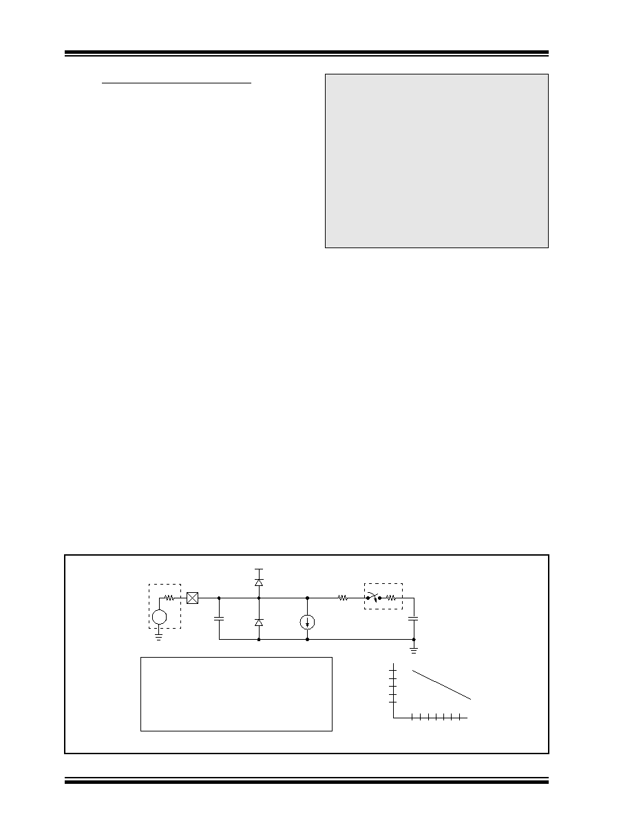
PIC16C9XX
DS30444E - page 82
©
1997 Microchip Technology Inc.
12.1
A/D Acquisition Requirements
For the A/D converter to meet its specified accuracy,
the charge holding capacitor (C
HOLD
) must be allowed
to fully charge to the input channel voltage level. The
analog input model is shown in Figure 12-4. The source
impedance (R
S
) and the internal sampling switch (R
SS
)
impedance directly affect the time required to charge
the capacitor C
HOLD
. The sampling switch (R
SS
) imped-
ance varies over the device voltage (V
DD
),
(Figure
12-4).
The source impedance affects the offset
voltage at the analog input (due to pin leakage current).
The maximum recommended impedance for ana-
log sources is 10 k
. After the analog input channel is
selected (changed) this acquisition must be done
before the conversion can be started.
To calculate the minimum acquisition time,
Equation
12-1 may be used. This equation calculates
the acquisition time to within 1/2 LSb error (512 steps
for the A/D). The 1/2 LSb error is the maximum error
allowed for the A/D to meet its specified accuracy.
EQUATION 12-1:
A/D MINIMUM CHARGING
TIME
V
HOLD
= (V
REF
- (V
REF
/512)) · (1 - e
(-Tc/C
HOLD
(R
IC
+ R
SS
+ R
S
))
)
Given: V
HOLD
= (V
REF
/512), for 1/2 LSb resolution
The above equation reduces to:
T
C
= -(51.2 pF)(1 k
- R
SS
+ R
S
) ln(1/511)
Example 12-1 shows the calculation of the minimum
required acquisition time (T
ACQ
). This calculation is
based on the following system assumptions.
C
HOLD
= 51.2 pF
Rs = 10 k
1/2 LSb error
V
DD
= 5V
Rss = 7 k
Temp (system max.) = 50
°
C
V
HOLD
= 0 @ t = 0
EXAMPLE 12-1: CALCULATING THE
MINIMUM REQUIRED
SAMPLE TIME
T
ACQ
= Amplifier Settling Time +
Holding Capacitor Charging Time +
Temperature Coefficient
T
ACQ
= 5
µ
s + Tc + [(Temp - 25
°
C)(0.05
µ
s/
°
C)]
T
C
=
-C
HOLD
(R
IC
+ R
SS
+ R
S
) ln(1/511)
-51.2 pF (1 k
+ 7 k
+ 10 k
) ln(0.0020)
-51.2 pF (18 k
) ln(0.0020)
-0.921
µ
s (-6.2364)
5.747
µ
s
T
ACQ
= 5
µ
s + 5.747
µ
s + [(50
°
C - 25
°
C)(0.05
µ
s/
°
C)]
10.747
µ
s + 1.25
µ
s
11.997
µ
s
Note 1: The reference voltage (V
REF
) has no
effect on the equation, since it cancels
itself out.
Note 2: The charge holding capacitor (C
HOLD
) is
not discharged after each conversion.
Note 3: The maximum recommended impedance
for analog sources is 10 k
. This is
required to meet the pin leakage specifi-
cation.
Note 4: After a conversion has completed, a
2.0
T
AD
delay must complete before
acquisition can begin again. During this
time the holding capacitor is not con-
nected to the selected A/D input channel.
FIGURE 12-4: ANALOG INPUT MODEL
C
PIN
VA
Rs
RAx
5 pF
V
DD
V
T
= 0.6V
V
T
= 0.6V
I leakage
R
IC
1k
Sampling
Switch
SS
R
SS
C
HOLD
= DAC capacitance
V
SS
6V
Sampling Switch
5V
4V
3V
2V
5 6 7 8 9 10 11
( k
)
V
DD
= 51.2 pF
±
500 nA
Legend C
PIN
V
T
I leakage
R
IC
SS
C
HOLD
= input capacitance
= threshold voltage
= leakage current at the pin due to
= interconnect resistance
= sampling switch
= sample/hold capacitance (from DAC)
various junctions
©
1997 Microchip Technology Inc.
DS30444E - page 83
PIC16C9XX
12.2
Selecting the A/D Conversion Clock
The A/D conversion time per bit is defined as T
AD
. The
A/D conversion requires 9.5 T
AD
per 8-bit conversion.
The source of the A/D conversion clock is software
selected. The four possible options for T
AD
are:
· 2T
OSC
· 8T
OSC
· 32T
OSC
· Internal RC oscillator
For correct A/D conversions, the A/D conversion clock
(T
AD
) must be selected to ensure a minimum T
AD
time
of 1.6
µ
s.
Table 12-1 shows the resultant T
AD
times derived from
the device operating frequencies and the A/D clock
source selected.
12.3
Configuring Analog Port Pins
The ADCON1 and TRISA registers control the opera-
tion of the A/D port pins. The port pins that are desired
as analog inputs must have their corresponding TRIS
bits set (input). If the TRIS bit is cleared (output), the
digital output level (V
OH
or V
OL
) will be converted.
The A/D operation is independent of the state of the
CHS2:CHS0 bits and the TRIS bits.
Note 1: When reading the port register, all pins
configured as analog inputs will read as
cleared (a low level). Pins configured as
digital inputs, will convert an analog input.
Analog levels on a digitally configured
input will not affect the conversion accu-
racy.
Note 2: Analog levels on any pin that is defined as
a digital input (including the AN4:AN0
pins), may cause the input buffer to con-
sume current that is out of the devices
specification.
TABLE 12-1: T
AD
vs. DEVICE OPERATING FREQUENCIES
A/D Clock Source (T
AD
)
Device Frequency
Operation
ADCS1:ADCS0
8 MHz
5 MHz
1.25 MHz
333.33 kHz
2T
OSC
00
250 ns
(2)
400 ns
(2)
1.6
µ
s
6
µ
s
8T
OSC
01
1
µ
s
1.6
µ
s
6.4
µ
s
24
µ
s
(3)
32T
OSC
10
4
µ
s
6.4
µ
s
25.6
µ
s
(3)
96
µ
s
(3)
RC
11
2 - 6
µ
s
(1,4)
2 - 6
µ
s
(1,4)
2 - 6
µ
s
(1,4)
2 - 6
µ
s
(1)
Legend: Shaded cells are outside of recommended range.
Note 1: The RC source has a typical T
AD
time of 4
µ
s.
2: These values violate the minimum required T
AD
time.
3: For faster conversion times, the selection of another clock source is recommended.
4: When derived frequency is greater than 1 MHz, the RC A/D conversion clock source is recommended for
sleep mode only
5: For extended voltage devices (LC), please refer to the electrical specifications section.

PIC16C9XX
DS30444E - page 84
©
1997 Microchip Technology Inc.
12.4
A/D Conversions
Example 12-2 show how to perform an A/D conversion.
The RA pins are configured as analog inputs. The ana-
log reference (V
REF
) is the device V
DD
. The A/D inter-
rupt is enabled, and the A/D conversion clock is F
RC
.
The conversion is performed on the RA0 pin
(channel0).
Note:
The GO/DONE bit should NOT be set in
the same instruction that turns on the A/D.
Clearing the GO/DONE bit during a conversion will
abort the current conversion. The ADRES register will
NOT be updated with the partially completed A/D con-
version sample. That is, the ADRES register will con-
tinue to contain the value of the last completed
conversion (or the last value written to the ADRES reg-
ister). After the A/D conversion is aborted, a 2T
AD
wait
is required before the next acquisition is started. After
this 2T
AD
wait, an acquisition is automatically started on
the selected channel.
EXAMPLE 12-2: DOING AN A/D CONVERSION
BCF STATUS, RP1 ; Select Bank1
BSF STATUS, RP0 ;
CLRF ADCON1 ; Configure A/D inputs
BSF PIE1, ADIE ; Enable A/D interrupts
BCF STATUS, RP0 ; Select Bank0
MOVLW 0xC1 ; RC Clock, A/D is on, Channel 0 is selected
MOVWF ADCON0 ;
BCF PIR1, ADIF ; Clear A/D interrupt flag bit
BSF INTCON, PEIE ; Enable peripheral interrupts
BSF INTCON, GIE ; Enable all interrupts
;
; Ensure that the required acquisition time for the selected input channel has elapsed.
; Then the conversion may be started.
;
BSF ADCON0, GO ; Start A/D Conversion
: ; The ADIF bit will be set and the GO/DONE bit
: ; is cleared upon completion of the A/D Conversion.
©
1997 Microchip Technology Inc.
DS30444E - page 85
PIC16C9XX
12.4.1
FASTER CONVERSION - LOWER
RESOLUTION TRADE-OFF
Not all applications require a result with 8-bits of reso-
lution, but may instead require a faster conversion time.
The A/D module allows users to make the trade-off of
conversion speed to resolution. Regardless of the res-
olution required, the acquisition time is the same. To
speed up the conversion, the clock source of the A/D
module may be switched so that the T
AD
time violates
the minimum specified time (see the applicable electri-
cal specification). Once the T
AD
time violates the mini-
mum specified time, all the following A/D result bits are
not valid (see A/D Conversion Timing in the Electrical
Specifications section.) The clock sources may only be
switched between the three oscillator versions (cannot
be switched from/to RC). The equation to determine
the time before the oscillator can be switched is as fol-
lows:
Conversion time = 2T
AD
+ N · T
AD
+ (8 - N)(2T
OSC
)
Where: N = number of bits of resolution required.
Since the T
AD
is based from the device oscillator, the
user must use some method (a timer, software loop,
etc.) to determine when the A/D oscillator may be
changed. Example 12-3 shows a comparison of time
required for a conversion with 4-bits of resolution, ver-
sus the 8-bit resolution conversion. The example is for
devices operating at 8 MHz (The A/D clock is pro-
grammed for 32T
OSC
), and assumes that immediately
after 6T
AD
, the A/D clock is programmed for 2T
OSC
.
The 2T
OSC
violates the minimum T
AD
time, therefore
the last 4-bits will not be converted to correct values.
EXAMPLE 12-3: 4-BIT vs. 8-BIT CONVERSION TIMES
Freq. (MHz)
Resolution
4-bit
8-bit
T
AD
8
1.6
µ
s
1.6
µ
s
T
OSC
8
12.5 ns
125 ns
2T
AD
+ N · T
AD
+ (8 - N)(2T
OSC
)
8
10.6
µ
s
16
µ
s

PIC16C9XX
DS30444E - page 86
©
1997 Microchip Technology Inc.
12.5
A/D Operation During Sleep
The A/D module can operate during SLEEP mode. This
requires that the A/D clock source be set to RC
(ADCS1:ADCS0 =
11
). When the RC clock source is
selected, the A/D module waits one instruction cycle
before starting the conversion. This allows the
SLEEP
instruction to be executed, which eliminates all digital
switching noise from the conversion. When the conver-
sion is completed the GO/DONE bit will be cleared, and
the result loaded into the ADRES register. If the A/D
interrupt is enabled, the device will wake-up from
SLEEP. If the A/D interrupt is not enabled, the A/D mod-
ule will then be turned off, although the ADON bit will
remain set.
When the A/D clock source is another clock option (not
RC), a
SLEEP
instruction will cause the present conver-
sion to be aborted and the A/D module to be turned off,
though the ADON bit will remain set.
Turning off the A/D places the A/D module in its lowest
current consumption state.
12.6
A/D Accuracy/Error
The absolute accuracy specified for the A/D converter
includes the sum of all contributions for quantization
error, integral error, differential error, full scale error, off-
set error, and monotonicity. It is defined as the maxi-
mum deviation from an actual transition versus an ideal
transition for any code. The absolute error of the A/D
converter is specified at <
±
1 LSb for V
DD
= V
REF
(over
the device's specified operating range). However, the
accuracy of the A/D converter will degrade as V
DD
diverges from V
REF
.
For a given range of analog inputs, the output digital
code will be the same. This is due to the quantization of
the analog input to a digital code. Quantization error is
typically
±
1/2 LSb and is inherent in the analog to dig-
ital conversion process. The only way to reduce quanti-
zation error is to increase the resolution of the A/D
converter.
Offset error measures the first actual transition of a
code versus the first ideal transition of a code. Offset
error shifts the entire transfer function. Offset error can
be calibrated out of a system or introduced into a sys-
tem through the interaction of the total leakage current
and source impedance at the analog input.
Gain error measures the maximum deviation of the last
actual transition and the last ideal transition adjusted for
offset error. This error appears as a change in slope of
the transfer function. The difference in gain error to full
Note:
For the A/D module to operate in SLEEP,
the A/D clock source must be set to RC
(ADCS1:ADCS0 =
11
). To perform an A/D
conversion in SLEEP, ensure the
SLEEP
instruction immediately follows the instruc-
tion that sets the GO/DONE bit.
scale error is that full scale does not take offset error
into account. Gain error can be calibrated out in soft-
ware.
Linearity error refers to the uniformity of the code
changes. Linearity errors cannot be calibrated out of
the system. Integral non-linearity error measures the
actual code transition versus the ideal code transition
adjusted by the gain error for each code.
Differential non-linearity measures the maximum actual
code width versus the ideal code width. This measure
is unadjusted.
The maximum pin leakage current is
±
1
µ
A.
In systems where the device frequency is low, use of
the A/D RC clock is preferred. At moderate to high fre-
quencies, T
AD
should be derived from the device oscil-
lator. T
AD
must not violate the minimum and should be
8
µ
s for preferred operation. This is because T
AD
,
when derived from T
OSC
, is kept away from on-chip
phase clock transitions. This reduces, to a large extent,
the effects of digital switching noise. This is not possible
with the RC derived clock. The loss of accuracy due to
digital switching noise can be significant if many I/O
pins are active.
In systems where the device will enter SLEEP mode
after the start of the A/D conversion, the RC clock
source selection is required. In this mode, the digital
noise from the modules in SLEEP are stopped. This
method gives high accuracy.
12.7
Effects of a RESET
A device reset forces all registers to their reset state.
This forces the A/D module to be turned off, and any
conversion is aborted.
The value that is in the ADRES register is not modified
for a Power-on Reset. The ADRES register will contain
unknown data after a Power-on Reset.
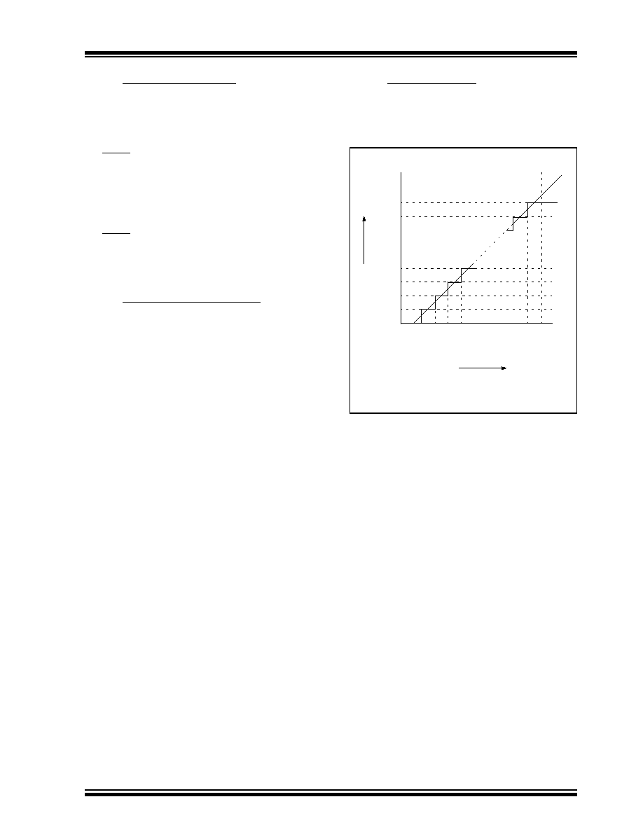
©
1997 Microchip Technology Inc.
DS30444E - page 87
PIC16C9XX
12.8
Use of the CCP Trigger
An A/D conversion can be started by the "special event
trigger" of the CCP1 module. This requires that the
CCP1M3:CCP1M0 bits (CCP1CON<3:0>) be pro-
grammed as
1011
and that the A/D module is enabled
(ADON bit is set). When the trigger occurs, the
GO/DONE bit will be set, starting the A/D conversion,
and the Timer1 counter will be reset to zero. Timer1 is
reset to automatically repeat the A/D acquisition period
with minimal software overhead (moving the ADRES to
the desired location). The appropriate analog input
channel must be selected and the minimum acquisition
done before the "special event trigger" sets the
GO/DONE bit (starts a conversion).
If the A/D module is not enabled (ADON is cleared),
then the "special event trigger" will be ignored by the
A/D module, but will still reset the Timer1 counter.
12.9
Connection Considerations
If the input voltage exceeds the rail values (V
SS
or V
DD
)
by greater than 0.2V, then the accuracy of the conver-
sion is out of specification.
An external RC filter is sometimes added for anti-alias-
ing of the input signal. The R component should be
selected to ensure that the total source impedance is
kept under the 10 k
recommended specification. Any
external components connected (via hi-impedance) to
an analog input pin (capacitor, zener diode, etc.) should
have very little leakage current at the pin.
12.10
Transfer Function
The ideal transfer function of the A/D converter is as fol-
lows: the first transition occurs when the analog input
voltage (V
AIN
) is Analog V
REF
/ 256 (Figure 12-5).
FIGURE 12-5: A/D TRANSFER FUNCTION
Digital code output
FFh
FEh
04h
03h
02h
01h
00h
0.5 LSb
1 LSb
2 LSb
3 LSb
4 LSb
255 LSb
256 LSb
(full scale)
Analog input voltage
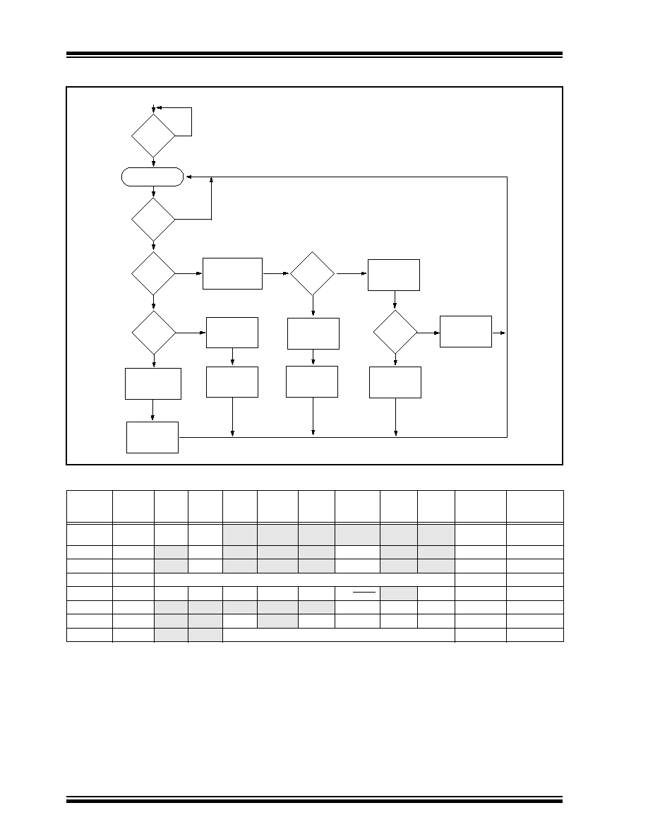
PIC16C9XX
DS30444E - page 88
©
1997 Microchip Technology Inc.
FIGURE 12-6: FLOWCHART OF A/D OPERATION
TABLE 12-2: SUMMARY OF A/D REGISTERS
Address
Name
Bit 7
Bit 6
Bit 5
Bit 4
Bit 3
Bit 2
Bit 1
Bit 0
Value on
Power-on
Reset
Value on all
other Resets
0Bh, 8Bh,
10Bh, 18Bh
INTCON
GIE
PEIE
T0IE
INTE
RBIE
T0IF
INTF
RBIF
0000 000x
0000 000u
0Ch
PIR1
LCDIF
ADIF
--
--
SSPIF
CCP1IF
TMR2IF
TMR1IF
00-- 0000
00-- 0000
8Ch
PIE1
LCDIE
ADIE
--
--
SSPIE
CCP1IE
TMR2IE
TMR1IE
00-- 0000
00-- 0000
1Eh
ADRES
A/D Result Register
xxxx xxxx
uuuu uuuu
1Fh
ADCON0
ADCS1
ADCS0
CHS2
CHS1
CHS0
GO/DONE
(1)
ADON
0000 0000
0000 0000
9Fh
ADCON1
--
--
--
--
--
PCFG2
PCFG1
PCFG0
---- -000
---- -000
05h
PORTA
--
--
RA5
RA4
RA3
RA2
RA1
RA0
--0x 0000
--0u 0000
85h
TRISA
--
--
PORTA Data Direction Control Register
--11 1111
--11 1111
Legend:
x
= unknown,
u
= unchanged,
-
= unimplemented read as '0'. Shaded cells are not used for A/D conversion.
Note
1: Bit1 of ADCON0 is reserved, always maintain this bit clear.
Acquire
ADON = 0
ADON = 0?
GO = 0?
A/D Clock
GO = 0
ADIF = 0
Abort Conversion
SLEEP
Power-down A/D
Wait 2 T
AD
Wake-up
Yes
No
Yes
No
No
Yes
Finish Conversion
GO = 0
ADIF = 1
Device in
No
Yes
Finish Conversion
GO = 0
ADIF = 1
Wait 2 T
AD
Stay in Sleep
Selected Channel
= RC?
SLEEP
No
Yes
Instruction?
Start of A/D
Conversion Delayed
1 Instruction Cycle
From Sleep?
Power-down A/D
Yes
No
Wait 2 T
AD
Finish Conversion
GO = 0
ADIF = 1
SLEEP?
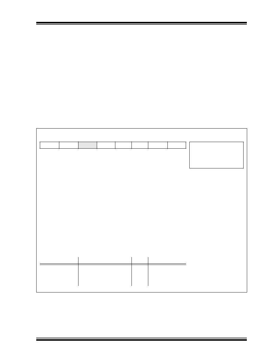
©
1997 Microchip Technology Inc.
DS30444E - page 89
PIC16C9XX
13.0
LCD MODULE
The LCD module generates the timing control to drive
a static or multiplexed LCD panel, with support for up to
32 segments multiplexed with up to 4 commons. It also
provides control of the LCD pixel data.
The interface to the module consists of 3 control regis-
ters (LCDCON, LCDSE, and LCDPS) used to define
the timing requirements of the LCD panel and up to 16
LCD data registers (LCD00-LCD15) that represent the
array of the pixel data. In normal operation, the control
registers are configured to match the LCD panel being
used. Primarily, the initialization information consists of
selecting the number of commons required by the LCD
panel, and then specifying the LCD Frame clock rate to
be used by the panel.
Once the module is initialized for the LCD panel, the
individual bits of the LCD data registers are cleared/set
to represent a clear/dark pixel respectively.
Once the module is configured, the LCDEN
(LCDCON<7>) bit is used to enable or disable the LCD
module. The LCD panel can also operate during sleep
by clearing the SLPEN (LCDCON<6>) bit.
Figure 13-4 through Figure 13-7 provides waveforms
for Static, 1/2, 1/3, and 1/4 MUX drives.
FIGURE 13-1: LCDCON REGISTER (ADDRESS 10Fh)
R/W-0
R/W-0
U-0
R/W-0
R/W-0
R/W-0
R/W-0
R/W-0
LCDEN
SLPEN
--
VGEN
CS1
CS0
LMUX1
LMUX0
R =Readable bit
W =Writable bit
U =Unimplemented bit,
Read as `0'
-n =Value at POR reset
bit7
bit0
bit 7:
LCDEN: Module drive enable bit
1 = LCD drive enabled
0 = LCD drive disabled
bit 6:
SLPEN: LCD display sleep enable
1 = LCD module will stop operating during SLEEP
0 = LCD module will continue to display during SLEEP
bit 5:
Unimplemented: Read as '0'
bit 4:
VGEN: Voltage Generator Enable
1 = Internal LCD Voltage Generator Enabled, (powered-up)
0 = Internal LCD Voltage Generator powered-down, voltage is expected to be provided externally
bit 3-2: CS1:CS0: Clock Source Select bits
00 = Fosc/256
01 = T1CKI (Timer1)
1x = Internal RC oscillator
bit 1-0:
LMUX1:LMUX0: Common Selection bits
Specifies the number of commons and the bias method
LMUX1:LMUX0
MULTIPLEX
BIAS
Max # of Segments
00
01
10
11
Static (COM0)
1/2
(COM0, 1)
1/3
(COM0, 1, 2)
1/4
(COM0, 1, 2, 3)
Static
1/3
1/3
1/3
32
31
30
29
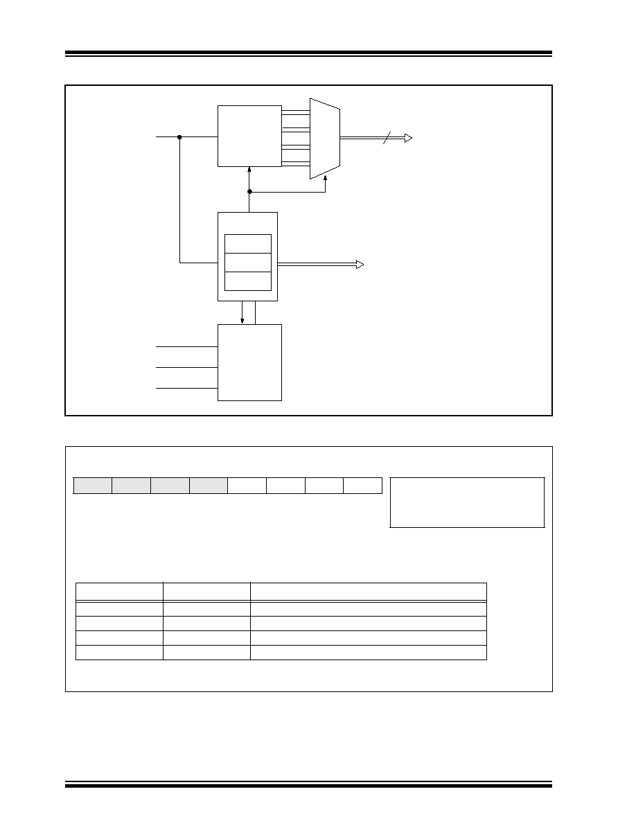
PIC16C9XX
DS30444E - page 90
©
1997 Microchip Technology Inc.
FIGURE 13-2: LCD MODULE BLOCK DIAGRAM
FIGURE 13-3: LCDPS REGISTER (ADDRESS 10Eh)
U-0
U-0
U-0
U-0
R/W-0
R/W-0
R/W-0
R/W-0
--
--
--
--
LP3
LP2
LP1
LP0
R =Readable bit
W =Writable bit
U =Unimplemented bit, Read as `0'
-n =Value at POR reset
bit7
bit0
bit 7-4:
Unimplemented, read as '0'
bit 3-0:
LP3:LP0: Frame Clock Prescale Selection bits
COM3:COM0
32 x 4
Clock
Source
Timing Control
Data Bus
Select
and
Divide
Internal RC osc
Fosc/4
T1CKI
RAM
128
to
32
MUX
SEG<31:0>
TO I/O PADS
TO I/O PADS
LCDCON
LCDPS
LCDSE
LCD
LMUX1:LMUX0
Multiplex
Frame Frequency =
00
Static
Clock source / (128 * (LP3:LP0 + 1))
01
1/2
Clock source / (128 * (LP3:LP0 + 1))
10
1/3
Clock source / (96 * (LP3:LP0 + 1))
11
1/4
Clock source / (128 * (LP3:LP0 + 1))
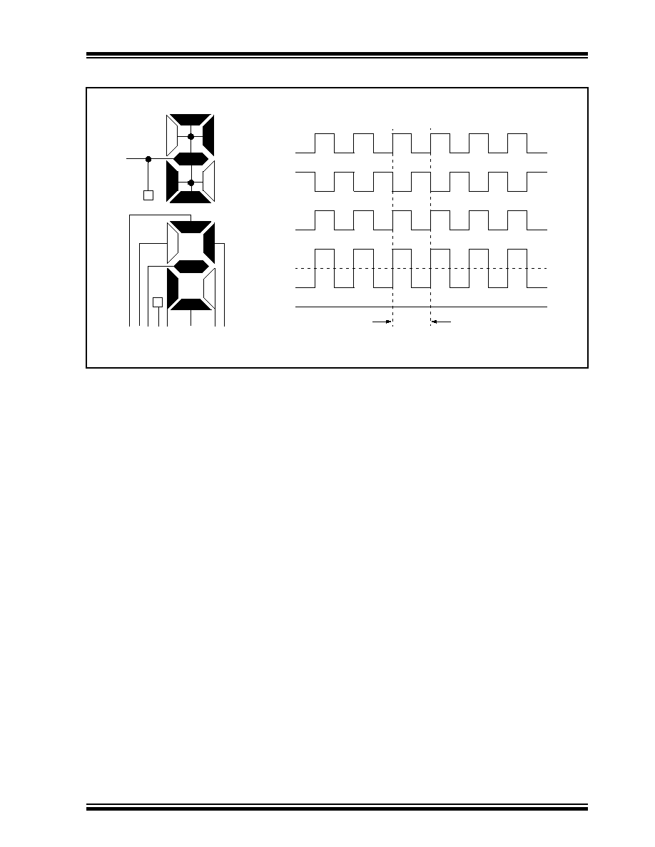
©
1997 Microchip Technology Inc.
DS30444E - page 91
PIC16C9XX
FIGURE 13-4: WAVEFORMS IN STATIC DRIVE
V
1
V
0
COM0
SEG0
COM0-SEG0
COM0-SEG1
SEG1
V
1
V
0
V
1
V
0
V
0
V
1
-V
1
V
0
1 Frame
COM0
SEG0
SEG1
SEG2
SEG3
SEG4
SEG5
SEG6
SEG7
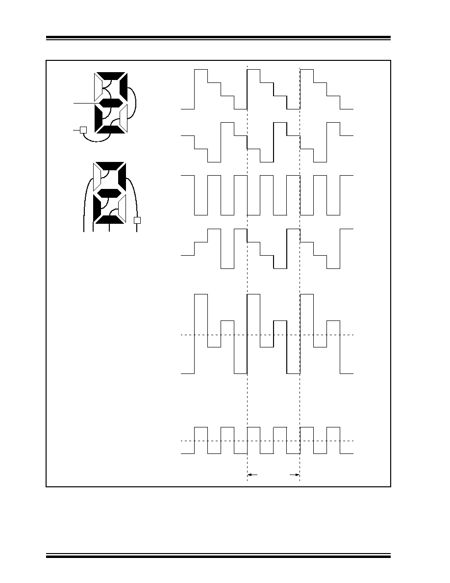
PIC16C9XX
DS30444E - page 92
©
1997 Microchip Technology Inc.
FIGURE 13-5: WAVEFORMS IN 1/2 MUX, 1/3 BIAS DRIVE
V
3
V
2
V
1
V
0
V
3
V
2
V
1
V
0
V
3
V
2
V
1
V
0
V
3
V
2
V
1
V
0
V
3
V
2
V
1
V
0
-V
3
-V
2
-V
1
V
3
V
2
V
1
V
0
-V
3
-V
2
-V
1
COM0
COM1
SEG0
SEG1
COM0-SEG0
COM0-SEG1
1 Frame
COM1
COM0
SEG0
SEG1
SEG2
SEG3
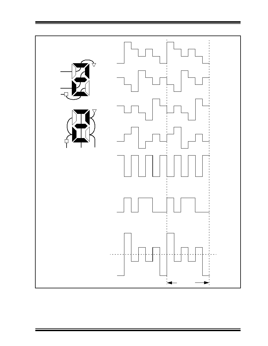
©
1997 Microchip Technology Inc.
DS30444E - page 93
PIC16C9XX
FIGURE 13-6: WAVEFORMS IN 1/3 MUX, 1/3 BIAS
V
3
V
2
V
1
V
0
V
3
V
2
V
1
V
0
V
3
V
2
V
1
V
0
V
3
V
2
V
1
V
0
V
3
V
2
V
1
V
0
V
3
V
2
V
1
V
0
-V
3
-V
2
-V
1
V
3
V
2
V
1
V
0
-V
3
-V
2
-V
1
COM0
COM1
COM2
SEG0
SEG1
COM0-SEG0
COM0-SEG1
1 Frame
COM2
COM1
COM0
SEG0
SEG1
SEG2
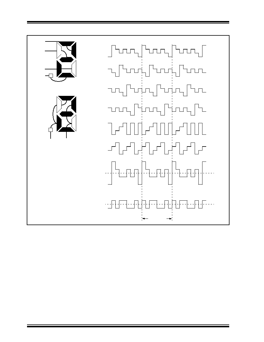
PIC16C9XX
DS30444E - page 94
©
1997 Microchip Technology Inc.
FIGURE 13-7: WAVEFORMS IN 1/4 MUX, 1/3 BIAS
V
3
V
2
V
1
V
0
V
3
V
2
V
1
V
0
V
3
V
2
V
1
V
0
V
3
V
2
V
1
V
0
V
3
V
2
V
1
V
0
V
3
V
2
V
1
V
0
V
3
V
2
V
1
V
0
-V
3
-V
2
-V
1
V
3
V
2
V
1
V
0
-V
3
-V
2
-V
1
COM0
COM1
COM2
COM3
SEG0
SEG1
COM0-SEG0
COM0-SEG1
COM3
COM2
COM1
COM0
1 Frame
SEG0
SEG1
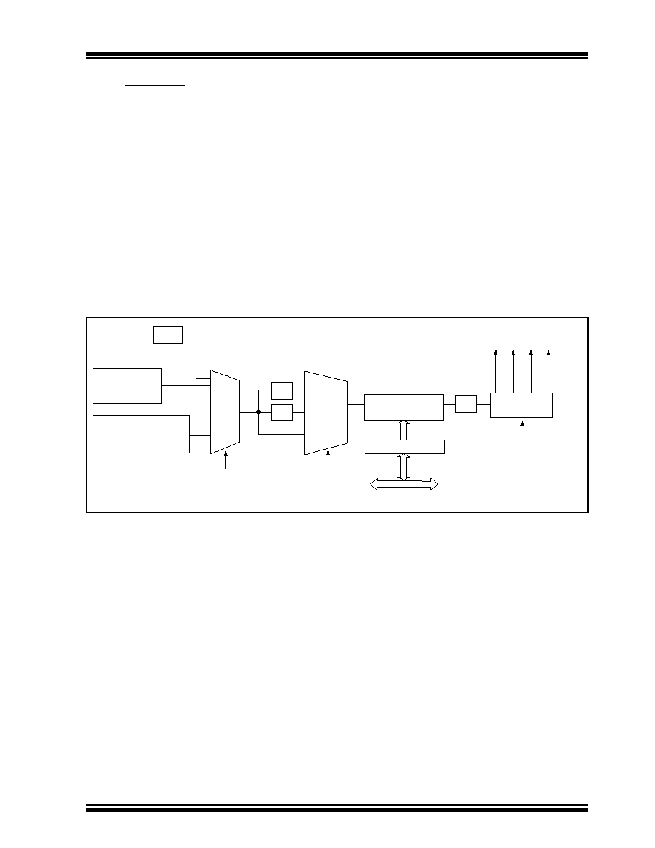
©
1997 Microchip Technology Inc.
DS30444E - page 95
PIC16C9XX
13.1
LCD Timing
The LCD module has 3 possible clock source inputs
and supports static, 1/2, 1/3, and 1/4 multiplexing.
13.1.1
TIMING CLOCK SOURCE SELECTION
The clock sources for the LCD timing generation are:
· Internal RC oscillator
· Timer1 oscillator
· System clock divided by 256
The first timing source is an internal RC oscillator which
runs at a nominal frequency of 14 kHz. This oscillator
provides a lower speed clock which may be used to
continue running the LCD while the processor is in
sleep. The RC oscillator will power-down when it is not
selected or when the LCD module is disabled.
The second source is the Timer1 external oscillator.
This oscillator provides a lower speed clock which may
be used to continue running the LCD while the proces-
sor is in sleep. It is assumed that the frequency pro-
vided on this oscillator will be 32 kHz. To use the
Timer1 oscillator as a LCD module clock source, it is
only necessary to set the T1OSCEN (T1CON<3>) bit.
The third source is the system clock divided by 256.
This divider ratio is chosen to provide about 32 kHz
output when the external oscillator is 8 MHz. The
divider is not programmable. Instead the LCDPS regis-
ter is used to set the LCD frame clock rate.
All of the clock sources are selected with bits CS1:CS0
(LCDCON<3:2>). Refer to Figure 13-1 for details of the
register programming.
FIGURE 13-8: LCD CLOCK GENERATION
CS1:CS0
TMR1 32 kHz
crystal oscillator
Internal RC oscillator
Nominal F
RC
= 14 kHz
Static
1/2
1/3
1/4
÷
4
÷
32
LMUX1:LMUX0
4-bit Programmable
LCDPS<3:0>
÷
1,2,3,4
Ring Counter
LMUX1:LMUX0
internal
data bus
COM2
÷
256
÷
2
F
OSC
Prescaler
COM0
COM1
COM3
PIC16C9XX
DS30444E - page 96
©
1997 Microchip Technology Inc.
13.1.2
MULTIPLEX TIMING GENERATION
The timing generation circuitry will generate 1 to 4 com-
mon clocks based on the display mode selected. The
mode is specified by bits LMUX1:LMUX0
(LCDCON<1:0>).
Table
13-1 shows the formulas for
calculating the frame frequency.
TABLE 13-1: FRAME FREQUENCY
FORMULAS
Multiplex
Frame Frequency =
Static
Clock source / (128 * (LP3:LP0 + 1))
1/2
Clock source / (128 * (LP3:LP0 + 1))
1/3
Clock source / (96 * (LP3:LP0 + 1))
1/4
Clock source / (128 * (LP3:LP0 + 1))
TABLE 13-2: APPROX. FRAME FREQ IN Hz
USING TIMER1 @ 32.768 kHz OR
Fosc @ 8 MHz
TABLE 13-3: APPROX. FRAME FREQ IN Hz
USING INTERNAL RC OSC @
14 kHz
LP3:LP0
Static
1/2
1/3
1/4
2
85
85
114
85
3
64
64
85
64
4
51
51
68
51
5
43
43
57
43
6
37
37
49
37
7
32
32
43
32
LP3:LP0
Static
1/2
1/3
1/4
0
109
109
146
109
1
55
55
73
55
2
36
36
49
36
3
27
27
36
27
©
1997 Microchip Technology Inc.
DS30444E - page 97
PIC16C9XX
13.2
LCD Interrupts
The LCD timing generation provides an interrupt that
defines the LCD frame timing. This interrupt can be
used to coordinate the writing of the pixel data with the
start of a new frame. Writing pixel data at the frame
boundary allows a visually crisp transition of the image.
This interrupt can also be used to synchronize external
events to the LCD. For example, the interface to an
external segment driver, such as a Microchip AY0438,
can be synchronized for segment data update to the
LCD frame.
A new frame is defined to begin at the leading edge of
the COM0 common signal. The interrupt will be set
immediately after the LCD controller completes
accessing all pixel data required for a frame. This will
occur at a certain fixed time before the frame boundary
as shown in Figure 13-9. The LCD controller will begin
to access data for the next frame within T
FWR
after the
interrupt.
FIGURE 13-9: EXAMPLE WAVEFORMS IN 1/4 MUX DRIVE
COM0
COM1
COM2
COM3
V3
V2
V1
V0
V3
V2
V1
V0
V3
V2
V1
V0
V3
V2
V1
V0
Frame
Boundary
Frame
Boundary
1 Frame
LCD
Interrupt
occurs
Controller accesses
next frame data
T
FINT
T
FWR
T
FWR
= T
FRAME
/(LMUX1:LMUX0 + 1)
T
FINT
= (T
FWR
/2 - (2T
CY
+ 40 ns))
min.
(T
FWR
/2 - (1T
CY
+ 40 ns))
max.
PIC16C9XX
DS30444E - page 98
©
1997 Microchip Technology Inc.
13.3
Pixel Control
13.3.1
LCDD (PIXEL DATA) REGISTERS
The pixel registers contain bits which define the state of
each pixel. Each bit defines one unique pixel.
Table 13-4 shows the correlation of each bit in the
LCDD registers to the respective common and seg-
ment signals.
Any LCD pixel location not being used for display can
be used as general purpose RAM.
FIGURE 13-10:GENERIC LCDD REGISTER LAYOUT
R/W-x
R/W-x
R/W-x
R/W-x
R/W-x
R/W-x
R/W-x
R/W-x
SEGs
COMc
SEGs
COMc
SEGs
COMc
SEGs
COMc
SEGs
COMc
SEGs
COMc
SEGs
COMc
SEGs
COMc
R =Readable bit
W =Writable bit
U =Unimplemented bit,
Read as `0'
-n =Value at POR reset
bit7
bit0
bit 7-0:
SEGsCOMc: Pixel Data Bit for segment s and common c
1 = Pixel on (dark)
0 = Pixel off (clear)
©
1997 Microchip Technology Inc.
DS30444E - page 99
PIC16C9XX
13.4
Operation During Sleep
The LCD module can operate during sleep. The selec-
tion is controlled by bit SLPEN (LCDCON<6>). Setting
the SLPEN bit allows the LCD module to go to sleep.
Clearing the SLPEN bit allows the module to continue
to operate during sleep.
If a
SLEEP
instruction is executed and SLPEN = '1', the
LCD module will cease all functions and go into a very
low current consumption mode. The module will stop
operation immediately and drive the minimum LCD
voltage on both segment and common lines. Figure
13-11 shows this operation. To ensure that the LCD
completes the frame, the
SLEEP
instruction should be
executed immediately after a LCD frame boundary.
The LCD interrupt can be used to determine the frame
boundary. See Section 13.2 for the formulas to calcu-
late the delay.
If a
SLEEP
instruction is executed and SLPEN = '0', the
module will continue to display the current contents of
the LCDD registers. To allow the module to continue
operation while in sleep, the clock source must be
either the internal RC oscillator or Timer1 external
oscillator. While in sleep, the LCD data cannot be
changed. The LCD module current consumption will
not decrease in this mode, however the overall con-
sumption of the device will be lower due to shutdown of
the core and other peripheral functions.
Note:
The internal RC oscillator or external
Timer1 oscillator must be used to operate
the LCD module during sleep.
FIGURE 13-11:SLEEP ENTRY/EXIT WHEN SLPEN = 1 OR CS1:CS0 = 00
COM0
COM1
COM3
3/3V
1/3V
0/3V
3/3V
3/3V
1/3V
2/3V
2/3V
1/3V
0/3V
2/3V
0/3V
3/3V
2/3V
1/3V
0/3V
SEG0
SLEEP
instruction execution
Wake-up
interrupted
frame
Pin
Pin
Pin
Pin

PIC16C9XX
DS30444E - page 100
©
1997 Microchip Technology Inc.
13.4.1
SEGMENT ENABLES
The LCDSE register is used to select the pin function
for groups of pins. The selection allows each group of
pins to operate as either LCD drivers or digital only
pins. To configure the pins as a digital port, the corre-
sponding bits in the LCDSE register must be cleared.
If the pin is a digital I/O the corresponding TRIS bit con-
trols the data direction. Any bit set in the LCDSE regis-
ter overrides any bit settings in the corresponding TRIS
register.
Note 1: On a Power-on Reset these pins are con-
figured as LCD drivers.
Note 2: The LMUX1:LMUX0 takes precedence
over the LCDSE bit settings for pins RD7,
RD6 and RD5.
EXAMPLE 13-1: STATIC MUX WITH 32
SEGMENTS
BCF STATUS,RP0 ;Select Bank 2
BSF STATUS,RP1 ;
BCF LCDCON,LMUX1 ;Select Static MUX
BCF LCDCON,LMUX0 ;
MOVLW 0xFF ;Make PortD,E,F,G
MOVWF LCDSE ;LCD pins
. . . ;configure rest of LCD
EXAMPLE 13-2: 1/3 MUX WITH 13
SEGMENTS
BCF STATUS,RP0 ;Select Bank 2
BSF STATUS,RP1 ;
BSF LCDCON,LMUX1 ;Select 1/3 MUX
BCF LCDCON,LMUX0 ;
MOVLW 0x87 ;Make PORTD<7:0> &
MOVWF LCDSE ;PORTE<6:0> LCD pins
. . . ;configure rest of LCD
FIGURE 13-12:LCDSE REGISTER (ADDRESS 10Dh)
R/W-1
R/W-1
R/W-1
R/W-1
R/W-1
R/W-1
R/W-1
R/W-1
SE29
SE27
SE20
SE16
SE12
SE9
SE5
SE0
R =Readable bit
W =Writable bit
U =Unimplemented bit,
Read as `0'
-n =Value at POR reset
bit7
bit0
bit 7:
SE29: Pin function select RD7/COM1/SEG31 - RD5/COM3/SEG29
1 = pins have LCD drive function
0 = pins have digital Input function
The LMUX1:LMUX0 setting takes precedence over the LCDSE register.
bit 6:
SE27: Pin function select RG7/SEG28 and RE7/SEG27
1 = pins have LCD drive function
0 = pins have digital Input function
bit 5:
SE20: Pin function select RG6/SEG26 - RG0/SEG20
1 = pins have LCD drive function
0 = pins have digital Input function
bit 4:
SE16: Pin function select RF7/SEG19 - RF4/SEG16
1 = pins have LCD drive function
0 = pins have digital Input function
bit 3:
SE12: Pin function select RF3/SEG15 - RF0/SEG12
1 = pins have LCD drive function
0 = pins have digital Input function
bit 2:
SE9: Pin function select RE6/SEG11 - RE4/SEG09
1 = pins have LCD drive function
0 = pins have digital Input function
bit 1:
SE5: Pin function select RE3/SEG08 - RE0/SEG05
1 = pins have LCD drive function
0 = pins have digital Input function
bit 0:
SE0: Pin function select RD4/SEG04 - RD0/SEG00
1 = pins have LCD drive function
0 = pins have digital I/O function
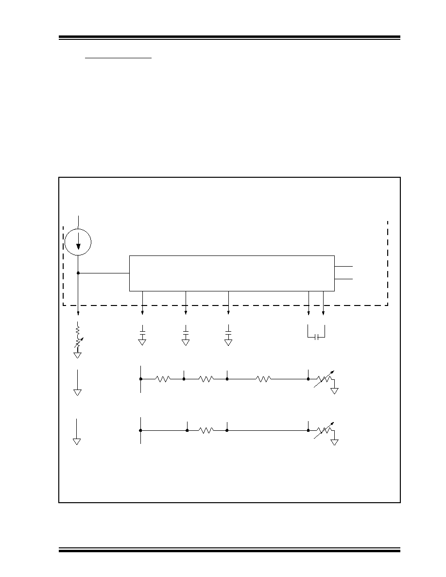
©
1997 Microchip Technology Inc.
DS30444E - page 101
PIC16C9XX
13.5
Voltage Generation
There are two methods for LCD voltage generation,
internal charge pump, or external resistor ladder.
13.5.1
CHARGE PUMP
The LCD charge pump is shown in Figure 13-13. The
1.0V - 2.3V regulator will establish a stable base volt-
age from the varying battery voltage. This regulator is
adjustable through the range by connecting a variable
external resistor from VLCDADJ to ground. The poten-
tiometer provides contrast adjustment for the LCD. This
base voltage is connected to V
LCD
1 on the charge
pump. The charge pump boosts V
LCD
1 into V
LCD
2 =
2*V
LCD
1 and V
LCD
3 = 3 * V
LCD
1. When the charge pump
is not operating, Vlcd3 will be internally tied to V
DD
. See
the Electrical Specifications section for charge pump
capacitor and potentiometer values.
13.5.2
EXTERNAL R-LADDER
The LCD module can also use an external resistor lad-
der (R-Ladder) to generate the LCD voltages.
Figure
13-13 shows external connections for static and
1/3 bias. The VGEN (LCDCON<4>) bit must be cleared
to use an external R-Ladder.
FIGURE 13-13:CHARGE PUMP AND RESISTOR LADDER
C2
V
LCD
2
V
LCD
1
V
LCD
3
C1
V
DD
VLCDADJ
10
µ
A
Connections for
internal charge
pump, VGEN = 1
V
DD
V
DD
Connections for
external R-ladder,
1/3 Bias,
VGEN = 0
Connections for
external R-ladder,
Static Bias,
VGEN = 0
nominal
Charge Pump
LCDEN
SLPEN
0.47
µ
F*
0.47
µ
F*
0.47
µ
F*
0.47
µ
F*
10k*
10k*
10k*
5k*
5k*
10k*
130k*
100k*
* These values are provided for design guidance only and should be
optimized to the application by the designer.
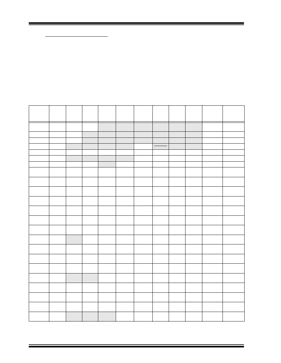
PIC16C9XX
DS30444E - page 102
©
1997 Microchip Technology Inc.
13.6
Configuring the LCD Module
The following is the sequence of steps to follow to con-
figure the LCD module.
1.
Select the frame clock prescale using bits
LP3:LP0 (LCDPS<3:0>).
2.
Configure the appropriate pins to function as
segment drivers using the LCDSE register.
3.
Configure the LCD module for the following
using the LCDCON register.
- Multiplex mode and Bias, bits
LMUX1:LMUX0
- Timing source, bits CS1:CS0
- Voltage generation, bit VGEN
- Sleep mode, bit SLPEN
4.
Write initial values to pixel data registers,
LCDD00 through LCDD15.
5.
Clear LCD interrupt flag, LCDIF (PIR1<7>), and
if desired, enable the interrupt by setting bit
LCDIE (PIE1<7>).
6.
Enable the LCD module, by setting bit LCDEN
(LCDCON<7>).
TABLE 13-4: SUMMARY OF REGISTERS ASSOCIATED WITH THE LCD MODULE
Address
Name
Bit 7
Bit 6
Bit 5
Bit 4
Bit 3
Bit 2
Bit 1
Bit 0
Value on
Power-on
Reset
Value on
all other
Resets
0Bh, 8Bh,
10Bh, 18Bh
INTCON
GIE
PEIE
T0IE
INTE
RBIE
T0IF
INTF
RBIF
0000 000x
0000 000u
0Ch
PIR1
LCDIF
ADIF
(1)
--
--
SSPIF
CCP1IF
TMR2IF
TMR1IF
00-- 0000
00-- 0000
8Ch
PIE1
LCDIE
ADIE
(1)
--
--
SSPIE
CCP1IE
TMR2IE
TMR1IE
00-- 0000
00-- 0000
10h
T1CON
--
--
T1CKPS1
T1CKPS0
T1OSCEN
T1SYNC
TMR1CS
TMR1ON
--00 0000
--uu uuuu
10Dh
LCDSE
SE29
SE27
SE20
SE16
SE12
SE9
SE5
SE0
1111 1111
1111 1111
10Eh
LCDPS
--
--
--
--
LP3
LP2
LP1
LP0
---- 0000
---- 0000
10Fh
LCDCON
LCDEN
SLPEN
--
VGEN
CS1
CS0
LMUX1
LMUX0
00-0 0000
00-0 0000
110h
LCDD00
SEG07
COM0
SEG06
COM0
SEG05
COM0
SEG04
COM0
SEG03
COM0
SEG02
COM0
SEG01
COM0
SEG00
COM0
xxxx xxxx
uuuu uuuu
111h
LCDD01
SEG15
COM0
SEG14
COM0
SEG13
COM0
SEG12
COM0
SEG11
COM0
SEG10
COM0
SEG09
COM0
SEG08
COM0
xxxx xxxx
uuuu uuuu
112h
LCDD02
SEG23
COM0
SEG22
COM0
SEG21
COM0
SEG20
COM0
SEG19
COM0
SEG18
COM0
SEG17
COM0
SEG16
COM0
xxxx xxxx
uuuu uuuu
113h
LCDD03
SEG31
COM0
SEG30
COM0
SEG29
COM0
SEG28
COM0
SEG27
COM0
SEG26
COM0
SEG25
COM0
SEG24
COM0
xxxx xxxx
uuuu uuuu
114h
LCDD04
SEG07
COM1
SEG06
COM1
SEG05
COM1
SEG04
COM1
SEG03
COM1
SEG02
COM1
SEG01
COM1
SEG00
COM1
xxxx xxxx
uuuu uuuu
115h
LCDD05
SEG15
COM1
SEG14
COM1
SEG13
COM1
SEG12
COM1
SEG11
COM1
SEG10
COM1
SEG09
COM1
SEG08
COM1
xxxx xxxx
uuuu uuuu
116h
LCDD06
SEG23
COM1
SEG22
COM1
SEG21
COM1
SEG20
COM1
SEG19
COM1
SEG18
COM1
SEG17
COM1
SEG16
COM1
xxxx xxxx
uuuu uuuu
117h
LCDD07
SEG31
COM1
(2)
SEG30
COM1
SEG29
COM1
SEG28
COM1
SEG27
COM1
SEG26
COM1
SEG25
COM1
SEG24
COM1
xxxx xxxx
uuuu uuuu
118h
LCDD08
SEG07
COM2
SEG06
COM2
SEG05
COM2
SEG04
COM2
SEG03
COM2
SEG02
COM2
SEG01
COM2
SEG00
COM2
xxxx xxxx
uuuu uuuu
119h
LCDD09
SEG15
COM2
SEG14
COM2
SEG13
COM2
SEG12
COM2
SEG11
COM2
SEG10
COM2
SEG09
COM2
SEG08
COM2
xxxx xxxx
uuuu uuuu
11Ah
LCDD10
SEG23
COM2
SEG22
COM2
SEG21
COM2
SEG20
COM2
SEG19
COM2
SEG18
COM2
SEG17
COM2
SEG16
COM2
xxxx xxxx
uuuu uuuu
11Bh
LCDD11
SEG31
COM2
(2)
SEG30
COM2
(2)
SEG29
COM2
SEG28
COM2
SEG27
COM2
SEG26
COM2
SEG25
COM2
SEG24
COM2
xxxx xxxx
uuuu uuuu
11Ch
LCDD12
SEG07
COM3
SEG06
COM3
SEG05
COM3
SEG04
COM3
SEG03
COM3
SEG02
COM3
SEG01
COM3
SEG00
COM3
xxxx xxxx
uuuu uuuu
11Dh
LCDD13
SEG15
COM3
SEG14
COM3
SEG13
COM3
SEG12
COM3
SEG11
COM3
SEG10
COM3
SEG09
COM3
SEG08
COM3
xxxx xxxx
uuuu uuuu
11Eh
LCDD14
SEG23
COM3
SEG22
COM3
SEG21
COM3
SEG20
COM3
SEG19
COM3
SEG18
COM3
SEG17
COM3
SEG16
COM3
xxxx xxxx
uuuu uuuu
11Fh
LCDD15
SEG31
COM3
(2)
SEG30
COM3
(2)
SEG29
COM3
(2)
SEG28
COM3
SEG27
COM3
SEG26
COM3
SEG25
COM3
SEG24
COM3
xxxx xxxx
uuuu uuuu
Legend:
x
= unknown,
u
= unchanged,
-
= unimplemented read as '0'. Shaded cells are not used by the LCD Module.
Note
1: These bits are reserved on the PIC16C923, always maintain these bits clear.
2: These pixels do not display, but can be used as general purpose RAM.
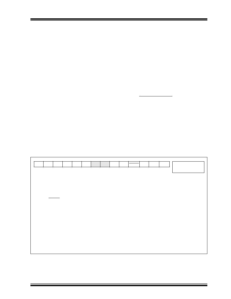
©
1997 Microchip Technology Inc.
DS30444E - page 103
PIC16C9XX
14.0
SPECIAL FEATURES OF THE
CPU
What sets a microcontroller apart from other proces-
sors are special circuits to deal with the needs of
real-time applications. The PIC16CXXX family has a
host of such features intended to maximize system reli-
ability, minimize cost through elimination of external
components, provide power saving operating modes
and offer code protection. These are:
· Oscillator selection
· Reset
- Power-on Reset (POR)
- Power-up Timer (PWRT)
- Oscillator Start-up Timer (OST)
· Interrupts
· Watchdog Timer (WDT)
· SLEEP
· Code protection
· ID locations
· In-circuit serial programming
The PIC16CXXX has a Watchdog Timer which can be
shut off only through configuration bits. It runs off its
own RC oscillator for added reliability. There are two
timers that offer necessary delays on power-up. One is
the Oscillator Start-up Timer (OST), intended to keep
the chip in reset until the crystal oscillator is stable. The
other is the Power-up Timer (PWRT), which provides a
fixed delay of 72 ms (nominal) on power-up only,
designed to keep the part in reset while the power sup-
ply stabilizes. With these two timers on-chip, most
applications need no external reset circuitry.
SLEEP mode is designed to offer a very low current
power-down mode. The user can wake-up from SLEEP
through external reset, Watchdog Timer Wake-up or
through an interrupt. Several oscillator options are also
made available to allow the part to fit the application.
The RC oscillator option saves system cost while the
LP crystal option saves power. A set of configuration
bits are used to select various options.
14.1
Configuration Bits
The configuration bits can be programmed (read as '0')
or left unprogrammed (read as '1') to select various
device configurations. These bits are mapped in pro-
gram memory location 2007h.
The user will note that address 2007h is beyond the
user program memory space. In fact, it belongs to the
special test/configuration memory space (2000h -
3FFFh), which can be accessed only during program-
ming.
FIGURE 14-1: CONFIGURATION WORD
CP1
CP0
CP1
CP0
CP1
CP0
--
--
CP1
CP0
PWRTE WDTE FOSC1 FOSC0
Register:
CONFIG
Address
2007h
bit13
bit0
bit 13-8 CP1:CP0 Code protection bits
(1)
5-4: 11 = Code protection off
10 = Upper half of program memory code protected
01 = Upper 3/4 of program memory code protected
00 = All memory is code protected
bit 6:
Unimplemented: Read as '1'
bit 3:
PWRTE: Power-up Timer Enable bit
1 = PWRT disabled
0 = PWRT enabled
bit 2:
WDTE: Watchdog Timer Enable bit
1 = WDT enabled
0 = WDT disabled
bit 1-0:
FOSC1:FOSC0: Oscillator Selection bits
11
= RC oscillator
10
= HS oscillator
01
= XT oscillator
00
= LP oscillator
Note
1: All of the CP1:CP0 bits have to be given the same value to enable the code protection scheme listed.
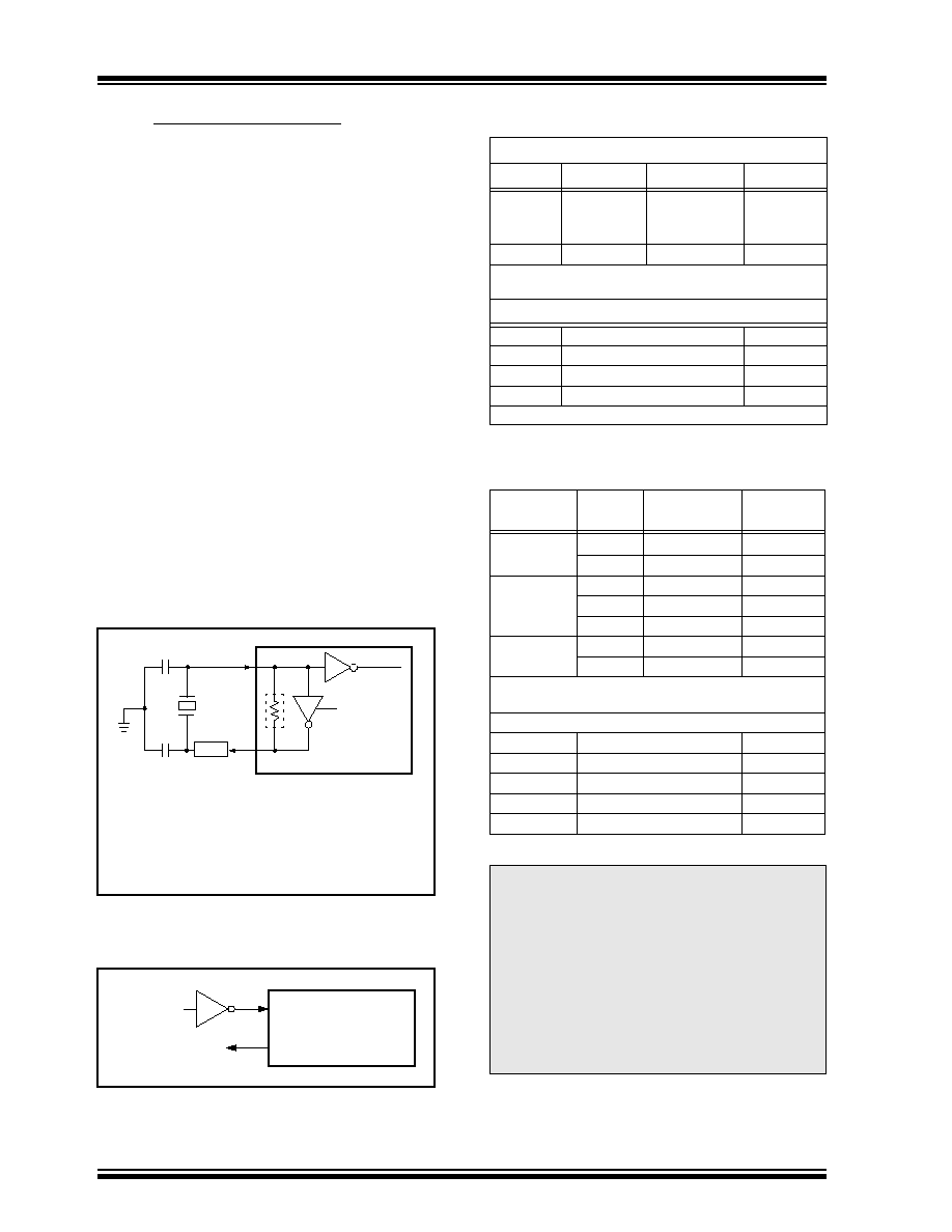
PIC16C9XX
DS30444E - page 104
©
1997 Microchip Technology Inc.
14.2
Oscillator Configurations
14.2.1
OSCILLATOR TYPES
The PIC16CXXX can be operated in four different oscil-
lator modes. The user can program two configuration
bits (FOSC1 and FOSC0) to select one of these four
modes:
· LP
Low Power Crystal
· XT
Crystal/Resonator
· HS
High Speed Crystal/Resonator
· RC
Resistor/Capacitor
14.2.2
CRYSTAL OSCILLATOR/CERAMIC
RESONATORS
In XT, LP or HS modes a crystal or ceramic resonator
is connected to the OSC1/CLKIN and OSC2/CLKOUT
pins to establish oscillation (Figure
14-2). The
PIC16CXXX oscillator design requires the use of a par-
allel cut crystal. Use of a series cut crystal may give a
frequency out of the crystal manufacturers specifica-
tions. When in XT, LP or HS modes, the device can
have an external clock source to drive the OSC1/CLKIN
pin (Figure 14-3).
FIGURE 14-2: CRYSTAL/CERAMIC
RESONATOR OPERATION
(HS, XT OR LP
OSC CONFIGURATION)
FIGURE 14-3: EXTERNAL CLOCK INPUT
OPERATION (HS, XT OR LP
OSC CONFIGURATION)
C1
C2
XTAL
OSC2
Note1
OSC1
R
F
SLEEP
To internal
logic
PIC16CXXX
RS
See Table 14-1 and Table 14-2 for recommended
values of C1 and C2.
Note 1: A series resistor may be required for AT
strip cut crystals.
OSC1
OSC2
Open
Clock from
ext. system
PIC16CXXX
TABLE 14-1: CERAMIC RESONATORS
TABLE 14-2: CAPACITOR SELECTION FOR
CRYSTAL OSCILLATOR
Ranges Tested:
Mode
Freq
OSC1
OSC2
XT
455 kHz
2.0 MHz
4.0 MHz
68 - 100 pF
15 - 68 pF
15 - 68 pF
68 - 100 pF
15 - 68 pF
15 - 68 pF
HS
8.0 MHz
10 - 68 pF
10 - 68 pF
These values are for design guidance only. See
notes at bottom of page.
Resonators Used:
455 kHz
Panasonic EFO-A455K04B
±
0.3%
2.0 MHz
Murata Erie CSA2.00MG
±
0.5%
4.0 MHz
Murata Erie CSA4.00MG
±
0.5%
8.0 MHz
Murata Erie CSA8.00MT
±
0.5%
All resonators used did not have built-in capacitors.
Osc Type
Crystal
Freq
Cap. Range
C1
Cap. Range
C2
LP
32 kHz
33 pF
33 pF
200 kHz
15 pF
15 pF
XT
200 kHz
47-68 pF
47-68 pF
1 MHz
15 pF
15 pF
4 MHz
15 pF
15 pF
HS
4 MHz
15 pF
15 pF
8 MHz
15-33 pF
15-33 pF
These values are for design guidance only. See
notes at bottom of page.
Crystals Used
32 kHz
Epson C-001R32.768K-A
±
20 PPM
200 kHz
STD XTL 200.000KHz
±
20 PPM
1 MHz
ECS ECS-10-13-1
±
50 PPM
4 MHz
ECS ECS-40-20-1
±
50 PPM
8 MHz
EPSON CA-301 8.000M-C
±
30 PPM
Note 1: Recommended values of C1 and C2 are
identical to the ranges tested (Table 14-1).
2: Higher capacitance increases the stability
of oscillator but also increases the start-up
time.
3: Since each resonator/crystal has its own
characteristics, the user should consult the
resonator/crystal manufacturer for appropri-
ate values of external components.
4: Rs may be required in HS mode as well as
XT mode to avoid overdriving crystals with
low drive level specification.
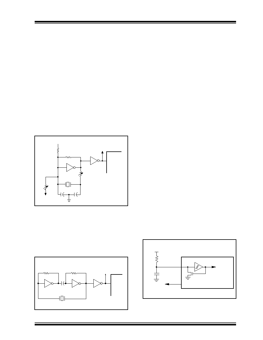
©
1997 Microchip Technology Inc.
DS30444E - page 105
PIC16C9XX
14.2.3
EXTERNAL CRYSTAL OSCILLATOR
CIRCUIT
Either a prepackaged oscillator can be used or a simple
oscillator circuit with TTL gates can be built. Prepack-
aged oscillators provide a wide operating range and
better stability. A well-designed crystal oscillator will
provide good performance with TTL gates. Two types of
crystal oscillator circuits can be used; one with series
resonance, or one with parallel resonance.
Figure 14-4 shows implementation of a parallel reso-
nant oscillator circuit. The circuit is designed to use the
fundamental frequency of the crystal. The 74AS04
inverter performs the 180-degree phase shift that a par-
allel oscillator requires. The 4.7 k
resistor provides the
negative feedback for stability. The 10 k
potentiometer
biases the 74AS04 in the linear region. This could be
used for external oscillator designs.
FIGURE 14-4: EXTERNAL PARALLEL
RESONANT CRYSTAL
OSCILLATOR CIRCUIT
Figure 14-5 shows a series resonant oscillator circuit.
This circuit is also designed to use the fundamental fre-
quency of the crystal. The inverter performs a
180-degree phase shift in a series resonant oscillator
circuit. The 330 k
resistors provide the negative feed-
back to bias the inverters in their linear region.
FIGURE 14-5: EXTERNAL SERIES
RESONANT CRYSTAL
OSCILLATOR CIRCUIT
20 pF
+5V
20 pF
10k
4.7k
10k
74AS04
XTAL
10k
74AS04
CLKIN
To Other
Devices
PIC16CXXX
330 k
74AS04
74AS04
PIC16CXXX
CLKIN
To Other
Devices
XTAL
330 k
74AS04
0.1
µ
F
14.2.4
RC OSCILLATOR
For timing insensitive applications the "RC" device
option offers additional cost savings. The RC oscillator
frequency is a function of the supply voltage, the resis-
tor (R
EXT
) and capacitor (C
EXT
) values, and the operat-
ing temperature. In addition to this, the oscillator
frequency will vary from unit to unit due to normal pro-
cess parameter variation. Furthermore, the difference
in lead frame capacitance between package types will
also affect the oscillation frequency, especially for low
C
EXT
values. The user also needs to take into account
variation due to tolerance of external R and C compo-
nents used. Figure 14-6 shows how the R/C combina-
tion is connected to the PIC16CXXX. For R
EXT
values
below 2.2 k
, the oscillator operation may become
unstable, or stop completely. For very high R
EXT
values
(e.g. 1 M
), the oscillator becomes sensitive to noise,
humidity and leakage. Thus, we recommend to keep
Rext between 3 k
and 100 k
.
Although the oscillator will operate with no external
capacitor (C
EXT
= 0 pF), we recommend using values
above 20 pF for noise and stability reasons. With no or
small external capacitance, the oscillation frequency
can vary dramatically due to changes in external
capacitances, such as PCB trace capacitance or pack-
age lead frame capacitance.
See characterization data for desired device for RC fre-
quency variation from part to part due to normal pro-
cess variation. The variation is larger for larger R (since
leakage current variation will affect RC frequency more
for large R) and for smaller C (since variation of input
capacitance will affect RC frequency more).
See characterization data for desired device for varia-
tion of oscillator frequency due to V
DD
for given
R
EXT
/C
EXT
values as well as frequency variation due to
operating temperature for given R, C, and V
DD
values.
The oscillator frequency, divided by 4, is available on
the OSC2/CLKOUT pin, and can be used for test pur-
poses or to synchronize other logic (see Figure 3-3 for
waveform).
FIGURE 14-6: RC OSCILLATOR MODE
OSC2/CLKOUT
C
EXT
V
DD
R
EXT
V
SS
PIC16CXXX
OSC1
Fosc/4
Internal
clock
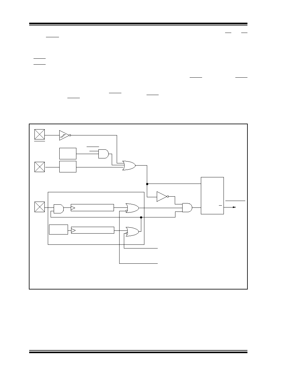
PIC16C9XX
DS30444E - page 106
©
1997 Microchip Technology Inc.
14.3
Reset
The PIC16CXX differentiates between various kinds of
reset:
· Power-on Reset (POR)
· MCLR Reset during normal operation
· MCLR Reset during SLEEP
· WDT Reset (normal operation)
Some registers are not affected in any reset condition;
their status is unknown on POR and unchanged in any
other reset. Most other registers are reset to a "reset
state" on Power-on Reset (POR), on the MCLR and
WDT Reset, and on MCLR Reset during SLEEP. They
are not affected by a WDT Wake-up, which is viewed as
the resumption of normal operation. The TO and PD
bits are set or cleared differently in different reset situ-
ations as indicated in Table 14-4. These bits are used
in software to determine the nature of the reset. See
Table 14-6 for a full description of reset states of all reg-
isters.
A simplified block diagram of the on-chip reset circuit is
shown in Figure 14-7.
The devices all have a MCLR noise filter in the MCLR
reset path. The filter will detect and ignore small pulses.
It should be noted that a WDT Reset
does not drive
MCLR pin low.
FIGURE 14-7: SIMPLIFIED BLOCK DIAGRAM OF ON-CHIP RESET CIRCUIT
S
R
Q
External
Reset
MCLR
V
DD
OSC1
WDT
Module
V
DD
rise
detect
OST/PWRT
On-chip
RC OSC
WDT
Time-out
Power-on Reset
OST
10-bit Ripple counter
PWRT
Chip_Reset
10-bit Ripple counter
Enable OST
(2)
Enable PWRT
(2)
SLEEP
Note
1: This is a separate oscillator from the RC oscillator of the CLKIN pin.
2: See Table 14-3 for time-out situations.
(1)
©
1997 Microchip Technology Inc.
DS30444E - page 107
PIC16C9XX
14.4
Power-on Reset (POR), Power-up
Timer (PWRT) and Oscillator Start-up
Timer (OST)
14.4.1
POWER-ON RESET (POR)
A Power-on Reset pulse is generated on-chip when
V
DD
rise is detected (in the range of 1.5V - 2.1V). To
take advantage of the POR, just tie the MCLR pin
directly (or through a resistor) to V
DD
. This will elimi-
nate external RC components usually needed to create
a Power-on Reset. A maximum rise time for V
DD
is
specified. See Electrical Specifications for details.
When the device starts normal operation (exits the
reset condition), device operating parameters (voltage,
frequency, temperature, ...) must be met to ensure
operation. If these conditions are not met, the device
must be held in reset until the operating conditions are
met.
For additional information, refer to Application Note
AN607, "
Power-up Trouble Shooting."
14.4.2
POWER-UP TIMER (PWRT)
The Power-up Timer provides a fixed 72 ms nominal
time-out on power-up only, from the POR. The
Power-up
Timer operates on an internal RC oscillator.
The chip is kept in reset as long as the PWRT is active.
The PWRT's time delay allows V
DD
to rise to an accept-
able level. A configuration bit is provided to enable/dis-
able the PWRT.
The power-up time delay will vary from chip to chip due
to V
DD
, temperature, and process variation. See DC
parameters for details.
14.4.3
OSCILLATOR START-UP TIMER (OST)
The Oscillator Start-up Timer (OST) provides 1024
oscillator cycle (from OSC1 input) delay after the
PWRT delay is over. This ensures that the crystal oscil-
lator or resonator has started and stabilized.
The OST time-out is invoked only for XT, LP and HS
modes and only on Power-on Reset or wake-up from
SLEEP.
14.4.4
TIME-OUT SEQUENCE
On power-up the time-out sequence is as follows: First
PWRT time-out is invoked after the POR time delay has
expired. Then OST is activated. The total time-out will
vary based on oscillator configuration and the status of
the PWRT. For example, in RC mode with the PWRT
disabled, there will be no time-out at all. Figure 14-8,
Figure 14-9, and Figure
14-10 depict time-out
sequences on power-up.
Since the time-outs occur from the POR pulse, if MCLR
is kept low long enough, the time-outs will expire. Then
bringing MCLR high will begin execution immediately
(Figure 14-9). This is useful for testing purposes or to
synchronize more than one PIC16CXXX device operat-
ing in parallel.
Table 14-5 shows the reset conditions for some special
function registers, while Table 14-6 shows the reset
conditions for all the registers.
14.4.5
POWER CONTROL/STATUS REGISTER
(PCON)
Bit1 is Power-on Reset Status bit POR. It is cleared on
a Power-on Reset and unaffected otherwise. The user
must set this bit following a Power-on Reset.
TABLE 14-3: TIME-OUT IN VARIOUS SITUATIONS
Oscillator Configuration
Power-up
Wake-up from SLEEP
PWRTE = 1
PWRTE = 0
XT, HS, LP
1024T
OSC
72 ms + 1024T
OSC
1024 T
OSC
RC
--
72 ms
--
PIC16C9XX
DS30444E - page 108
©
1997 Microchip Technology Inc.
TABLE 14-4: STATUS BITS AND THEIR SIGNIFICANCE
TABLE 14-5: RESET CONDITION FOR SPECIAL REGISTERS
POR
TO
PD
0
1
1
Power-on Reset
0
0
x
Illegal, TO is set on POR
0
x
0
Illegal, PD is set on POR
1
0
1
WDT Reset
1
0
0
WDT Wake-up
1
u
u
MCLR Reset during normal operation
1
1
0
MCLR Reset during SLEEP or interrupt wake-up from SLEEP
Legend:
u
= unchanged,
x
= unknown
Condition
Program
Counter
STATUS
Register
PCON
Register
Power-on Reset
000h
0001 1xxx
---- --0-
MCLR Reset during normal operation
000h
000u uuuu
---- --u-
MCLR Reset during SLEEP
000h
0001 0uuu
---- --u-
WDT Reset
000h
0000 1uuu
---- --u-
WDT Wake-up
PC + 1
uuu0 0uuu
---- --u-
Interrupt wake-up from SLEEP
PC + 1
(1)
uuu1 0uuu
---- --u-
Legend:
u
= unchanged,
x
= unknown,
-
= unimplemented bit read as '0'.
Note 1: When the wake-up is due to an interrupt and the GIE bit is set, the PC is loaded
with the interrupt vector (0004h).
TABLE 14-6: INITIALIZATION CONDITIONS FOR ALL REGISTERS
Register
Applicable Devices
Power-on Reset
MCLR Resets
WDT Reset
Wake-up via
WDT or
Interrupt
W
923
924
xxxx xxxx
uuuu uuuu
uuuu uuuu
INDF
923
924
N/A
N/A
N/A
TMR0
923
924
xxxx xxxx
uuuu uuuu
uuuu uuuu
PCL
923
924
0000h
0000h
PC + 1
(2)
STATUS
923
924
0001 1xxx
000q quuu
(3)
uuuq quuu
(3)
FSR
923
924
xxxx xxxx
uuuu uuuu
uuuu uuuu
PORTA
923
924
--xx xxxx
--uu uuuu
--uu uuuu
PORTA
923
924
--0x 0000
(5)
--0u 0000
(5)
--uu uuuu
PORTB
923
924
xxxx xxxx
uuuu uuuu
uuuu uuuu
PORTC
923
924
--xx xxxx
--uu uuuu
--uu uuuu
Legend:
u
= unchanged,
x
= unknown,
-
= unimplemented bit, read as '0',
q
= value depends on condition
Note 1: One or more bits in INTCON and/or PIR1 will be affected (to cause wake-up).
2: When the wake-up is due to an interrupt and the GIE bit is set, the PC is loaded with the interrupt vector
(0004h).
3: See Table 14-5 for reset value for specific condition.
4: Bits PIE1<6> and PIR1<6> are reserved on the PIC16C923, always maintain these bits clear.
5: PORTA values when read.
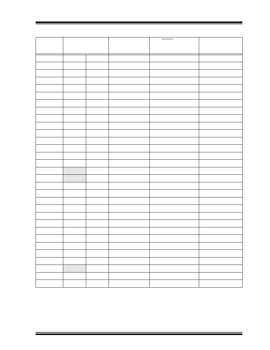
©
1997 Microchip Technology Inc.
DS30444E - page 109
PIC16C9XX
PORTD
923
924
0000 0000
0000 0000
uuuu uuuu
PORTE
923
924
0000 0000
0000 0000
uuuu uuuu
PCLATH
923
924
---0 0000
---0 0000
---u uuuu
INTCON
923
924
0000 000x
0000 000u
uuuu uuuu
(1)
PIR1
(4)
923
924
00-- 0000
00-- 0000
uu-- uuuu
(1)
TMR1L
923
924
xxxx xxxx
uuuu uuuu
uuuu uuuu
TMR1H
923
924
xxxx xxxx
uuuu uuuu
uuuu uuuu
T1CON
923
924
--00 0000
--uu uuuu
--uu uuuu
TMR2
923
924
0000 0000
0000 0000
uuuu uuuu
T2CON
923
924
-000 0000
-000 0000
-uuu uuuu
SSPBUF
923
924
xxxx xxxx
uuuu uuuu
uuuu uuuu
SSPCON
923
924
0000 0000
0000 0000
uuuu uuuu
CCPR1L
923
924
xxxx xxxx
uuuu uuuu
uuuu uuuu
CCPR1H
923
924
xxxx xxxx
uuuu uuuu
uuuu uuuu
CCP1CON
923
924
--00 0000
--00 0000
--uu uuuu
ADRES
923
924
xxxx xxxx
uuuu uuuu
uuuu uuuu
ADCON0
923
924
0000 00-0
0000 00-0
uuuu uu-u
OPTION
923
924
1111 1111
1111 1111
uuuu uuuu
TRISA
923
924
--11 1111
--11 1111
--uu uuuu
TRISB
923
924
1111 1111
1111 1111
uuuu uuuu
TRISC
923
924
--11 1111
--11 1111
--uu uuuu
TRISD
923
924
1111 1111
1111 1111
uuuu uuuu
TRISE
923
924
1111 1111
1111 1111
uuuu uuuu
PIE1
(4)
923
924
00-- 0000
00-- 0000
uu-- uuuu
PCON
923
924
---- --0-
---- --u-
---- --u-
PR2
923
924
1111 1111
1111 1111
1111 1111
SSPADD
923
924
0000 0000
0000 0000
uuuu uuuu
SSPSTAT
923
924
0000 0000
0000 0000
uuuu uuuu
ADCON1
923
924
---- -000
---- -000
---- -uuu
PORTF
923
924
0000 0000
0000 0000
uuuu uuuu
PORTG
923
924
0000 0000
0000 0000
uuuu uuuu
TABLE 14-6: INITIALIZATION CONDITIONS FOR ALL REGISTERS (Cont.'d)
Register
Applicable Devices
Power-on Reset
MCLR Resets
WDT Reset
Wake-up via
WDT or
Interrupt
Legend:
u
= unchanged,
x
= unknown,
-
= unimplemented bit, read as '0',
q
= value depends on condition
Note 1: One or more bits in INTCON and/or PIR1 will be affected (to cause wake-up).
2: When the wake-up is due to an interrupt and the GIE bit is set, the PC is loaded with the interrupt vector
(0004h).
3: See Table 14-5 for reset value for specific condition.
4: Bits PIE1<6> and PIR1<6> are reserved on the PIC16C923, always maintain these bits clear.
5: PORTA values when read.
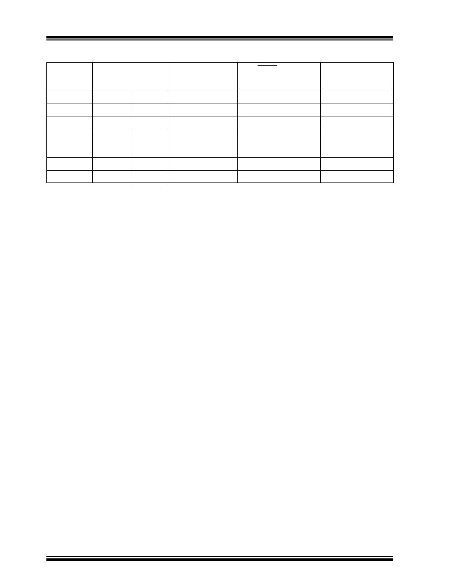
PIC16C9XX
DS30444E - page 110
©
1997 Microchip Technology Inc.
LCDSE
923
924
1111 1111
1111 1111
uuuu uuuu
LCDPS
923
924
---- 0000
---- 0000
---- uuuu
LCDCON
923
924
00-0 0000
00-0 0000
uu-u uuuu
LCDD00
to
LCDD15
923
924
xxxx xxxx
uuuu uuuu
uuuu uuuu
TRISF
923
924
1111 1111
1111 1111
uuuu uuuu
TRISG
923
924
1111 1111
1111 1111
uuuu uuuu
TABLE 14-6: INITIALIZATION CONDITIONS FOR ALL REGISTERS (Cont.'d)
Register
Applicable Devices
Power-on Reset
MCLR Resets
WDT Reset
Wake-up via
WDT or
Interrupt
Legend:
u
= unchanged,
x
= unknown,
-
= unimplemented bit, read as '0',
q
= value depends on condition
Note 1: One or more bits in INTCON and/or PIR1 will be affected (to cause wake-up).
2: When the wake-up is due to an interrupt and the GIE bit is set, the PC is loaded with the interrupt vector
(0004h).
3: See Table 14-5 for reset value for specific condition.
4: Bits PIE1<6> and PIR1<6> are reserved on the PIC16C923, always maintain these bits clear.
5: PORTA values when read.
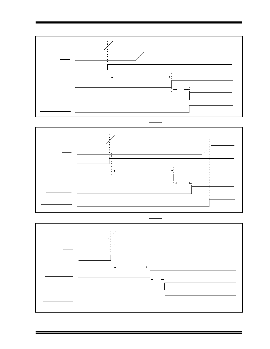
©
1997 Microchip Technology Inc.
DS30444E - page 111
PIC16C9XX
FIGURE 14-8: TIME-OUT SEQUENCE ON POWER-UP (MCLR NOT TIED TO V
DD
): CASE 1
FIGURE 14-9: TIME-OUT SEQUENCE ON POWER-UP (MCLR NOT TIED TO V
DD
): CASE 2
FIGURE 14-10:TIME-OUT SEQUENCE ON POWER-UP (MCLR TIED TO V
DD
)
T
PWRT
T
OST
V
DD
MCLR
INTERNAL POR
PWRT TIME-OUT
OST TIME-OUT
INTERNAL RESET
V
DD
MCLR
INTERNAL POR
PWRT TIME-OUT
OST TIME-OUT
INTERNAL RESET
T
PWRT
T
OST
T
PWRT
T
OST
V
DD
MCLR
INTERNAL POR
PWRT TIME-OUT
OST TIME-OUT
INTERNAL RESET
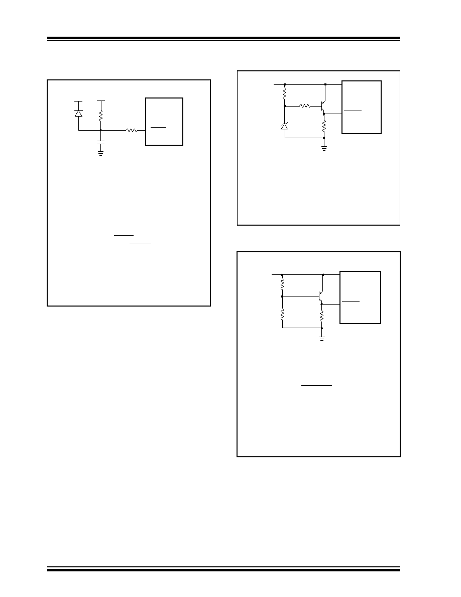
PIC16C9XX
DS30444E - page 112
©
1997 Microchip Technology Inc.
FIGURE 14-11:EXTERNAL POWER-ON
RESET CIRCUIT (FOR SLOW
V
DD
POWER-UP)
Note 1: External Power-on Reset circuit is required
only if V
DD
power-up slope is too slow. The
diode D helps discharge the capacitor
quickly when V
DD
powers down.
2: R < 40 k
is recommended to make sure
that voltage drop across R does not violate
the device's electrical specification.
3: R1 = 100
to 1 k
will limit any current
flowing into MCLR from external capacitor
C in the event of MCLR/V
PP
pin break-
down due to Electrostatic Discharge
(ESD) or Electrical Overstress (EOS).
C
R1
R
D
V
DD
MCLR
PIC16CXXX
FIGURE 14-12:EXTERNAL BROWN-OUT
PROTECTION CIRCUIT 1
FIGURE 14-13:EXTERNAL BROWN-OUT
PROTECTION CIRCUIT 2
Note 1: This circuit will activate reset when V
DD
goes below (Vz + 0.7V) where Vz = Zener
voltage.
2: Resistors should be adjusted for the char-
acteristics of the transistors.
V
DD
33k
10k
40k
V
DD
MCLR
PIC16CXXX
Note 1: This brown-out circuit is less expensive,
albeit less accurate. Transistor Q1 turns
off when V
DD
is below a certain level
such that:
2: Resistors should be adjusted for the
characteristics of the transistors.
V
DD
·
R1
R1 + R2
= 0.7V
V
DD
R2
40k
V
DD
MCLR
PIC16CXXX
R1
Q1
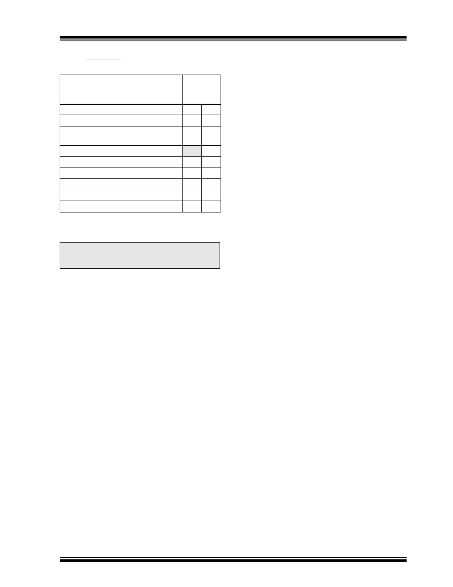
©
1997 Microchip Technology Inc.
DS30444E - page 113
PIC16C9XX
14.5
Interrupts
The PIC16C9XX family has up to 9 sources of interrupt:
The interrupt control register (INTCON) records individ-
ual interrupt requests in flag bits. It also has individual
and global interrupt enable bits.
Interrupt Sources
Applicable
Devices
External interrupt RB0/INT
923
924
TMR0 overflow interrupt
923
924
PORTB change interrupts
(pins RB7:RB4)
923
924
A/D Interrupt
923
924
TMR1 overflow interrupt
923
924
TMR2 matches period interrupt
923
924
CCP1 interrupt
923
924
Synchronous serial port interrupt
923
924
LCD Module interrupt
923
924
Note:
Individual interrupt flag bits are set regard-
less of the status of their corresponding
mask bit or the GIE bit.
A global interrupt enable bit, GIE (INTCON<7>)
enables (if set) all un-masked interrupts or disables (if
cleared) all interrupts. When bit GIE is enabled, and an
interrupt's flag bit and mask bit are set, the interrupt will
vector immediately. Individual interrupts can be dis-
abled through their corresponding enable bits in various
registers. Individual interrupt bits are set regardless of
the status of the GIE bit. The GIE bit is cleared on reset.
The "return from interrupt" instruction,
RETFIE
, exits
the interrupt routine as well as sets the GIE bit, which
re-enables interrupts.
The RB0/INT pin interrupt, the RB port change interrupt
and the TMR0 overflow interrupt flags are contained in
the INTCON register.
The peripheral interrupt flags are contained in the spe-
cial function register PIR1. The corresponding interrupt
enable bits are contained in special function register
PIE1, and the peripheral interrupt enable bit is con-
tained in special function register INTCON.
When an interrupt is responded to, the GIE bit is
cleared to disable any further interrupts, the return
address is pushed onto the stack and the PC is loaded
with 0004h. Once in the interrupt service routine the
source(s) of the interrupt can be determined by polling
the interrupt flag bits. The interrupt flag bit(s) must be
cleared in software before re-enabling interrupts to
avoid recursive interrupts.
For external interrupt events, such as the RB0/INT pin
or RB Port change interrupt, the interrupt latency will be
three or four instruction cycles. The exact latency
depends when the interrupt event occurs
(Figure
14-15).
The latency is the same for one or two
cycle instructions. Individual interrupt flag bits are set
regardless of the status of their corresponding mask bit
or the GIE bit.
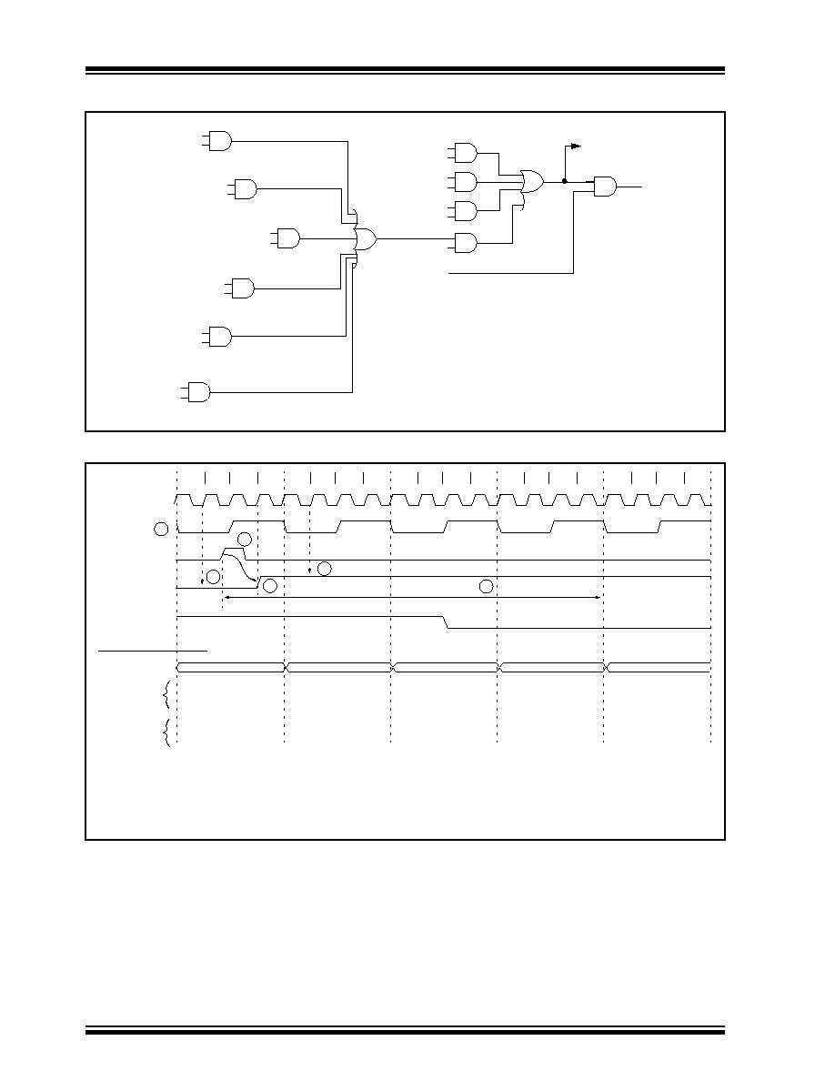
PIC16C9XX
DS30444E - page 114
©
1997 Microchip Technology Inc.
FIGURE 14-14:INTERRUPT LOGIC
FIGURE 14-15:INT PIN INTERRUPT TIMING
TMR1IF
TMR1IE
TMR2IF
TMR2IE
CCP1IF
CCP1IE
LCDIF
LCDIE
SSPIF
SSPIE
T0IF
T0IE
INTF
INTE
RBIF
RBIE
GIE
PEIE
Wake-up (If in SLEEP mode)
Interrupt to CPU
PEIF
ADIF
ADIE
The A/D module interrupt is implemented on the PIC16C924 only.
Q2
Q1
Q3
Q4
Q2
Q1
Q3
Q4
Q2
Q1
Q3
Q4
Q2
Q1
Q3
Q4
Q2
Q1
Q3
Q4
OSC1
CLKOUT
INT pin
INTF flag
(INTCON<1>)
GIE bit
(INTCON<7>)
INSTRUCTION FLOW
PC
Instruction
fetched
Instruction
executed
Interrupt Latency
PC
PC+1
PC+1
0004h
0005h
Inst (0004h)
Inst (0005h)
Dummy Cycle
Inst (PC)
Inst (PC+1)
Inst (PC-1)
Inst (0004h)
Dummy Cycle
Inst (PC)
--
1
4
5
1
Note 1: INTF flag is sampled here (every Q1).
2: Interrupt latency = 3-4 T
CY
where T
CY
= instruction cycle time.
Latency is the same whether Inst (PC) is a single cycle or a 2-cycle instruction.
3: CLKOUT is available only in RC oscillator mode.
4: For minimum width of INT pulse, refer to AC specs.
5: INTF can be set anytime during the Q4-Q1 cycles.
2
3

©
1997 Microchip Technology Inc.
DS30444E - page 115
PIC16C9XX
14.5.1
INT INTERRUPT
External interrupt on RB0/INT pin is edge triggered:
either rising if bit INTEDG (OPTION<6>) is set, or fall-
ing, if the INTEDG bit is clear. When a valid edge
appears on the RB0/INT pin, flag bit INTF
(INTCON<1>) is set. This interrupt can be disabled by
clearing enable bit INTE (INTCON<4>). Flag bit INTF
must be cleared in software in the interrupt service rou-
tine before re-enabling this interrupt. The INT interrupt
can wake-up the processor from SLEEP, if bit INTE was
set prior to going into SLEEP. The status of global inter-
rupt enable bit GIE decides whether or not the proces-
sor branches to the interrupt vector following wake-up.
See Section 14.8 for details on SLEEP mode.
14.5.2
TMR0 INTERRUPT
An overflow (FFh
00h) in the TMR0 register will set
flag bit T0IF (INTCON<2>). The interrupt can be
enabled/disabled by setting/clearing enable bit T0IE
(INTCON<5>). (Section 7.0)
14.5.3
PORTB INTCON CHANGE
An input change on PORTB<7:4> sets flag bit RBIF
(INTCON<0>). The interrupt can be enabled/disabled
by setting/clearing enable bit RBIE (INTCON<4>).
(Section 5.2)
14.6
Context Saving During Interrupts
During an interrupt, only the return PC value is saved
on the stack. Typically, users may wish to save key reg-
isters during an interrupt i.e., W register and STATUS
register. This will have to be implemented in software.
Example 14-1 stores and restores the STATUS, W, and
PCLATH registers. The register, W_TEMP, must be
defined in each bank and must be defined at the same
offset from the bank base address (i.e., if W_TEMP is
defined at 0x20 in bank 0, it must also be defined at
0xA0 in bank 1).
The example:
a)
Stores the W register.
b)
Stores the STATUS register in bank 0.
c)
Stores the PCLATH register.
d)
Executes the ISR code.
e)
Restores the STATUS register (and bank select
bit).
f)
Restores the W and PCLATH registers.
EXAMPLE 14-1: SAVING STATUS, W, AND PCLATH REGISTERS IN RAM
MOVWF W_TEMP ;Copy W to TEMP register, could be bank one or zero
SWAPF STATUS,W ;Swap status to be saved into W
CLRF STATUS ;bank 0, regardless of current bank, Clears IRP,RP1,RP0
MOVWF STATUS_TEMP ;Save status to bank zero STATUS_TEMP register
MOVF PCLATH, W ;Only required if using pages 1, 2 and/or 3
MOVWF PCLATH_TEMP ;Save PCLATH into W
CLRF PCLATH ;Page zero, regardless of current page
BCF STATUS, IRP ;Return to Bank 0
MOVF FSR, W ;Copy FSR to W
MOVWF FSR_TEMP ;Copy FSR from W to FSR_TEMP
:
:(ISR)
:
MOVF PCLATH_TEMP, W ;Restore PCLATH
MOVWF PCLATH ;Move W into PCLATH
SWAPF STATUS_TEMP,W ;Swap STATUS_TEMP register into W
;(sets bank to original state)
MOVWF STATUS ;Move W into STATUS register
SWAPF W_TEMP,F ;Swap W_TEMP
SWAPF W_TEMP,W ;Swap W_TEMP into W
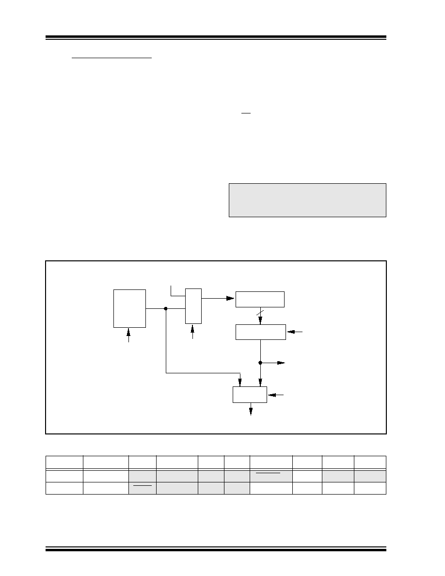
PIC16C9XX
DS30444E - page 116
©
1997 Microchip Technology Inc.
14.7
Watchdog Timer (WDT)
The Watchdog Timer is as a free running on-chip RC
oscillator which does not require any external compo-
nents. This RC oscillator is separate from the RC oscil-
lator of the OSC1/CLKIN pin. That means that the WDT
will run, even if the clock on the OSC1/CLKIN and
OSC2/CLKOUT pins of the device has been stopped,
for example, by execution of a
SLEEP
instruction. Dur-
ing normal operation, a WDT time-out generates a
device RESET (Watchdog Timer Reset). If the device is
in SLEEP mode, a WDT time-out causes the device to
wake-up and continue with normal operation (Watch-
dog Timer Wake-up). The WDT can be permanently
disabled by clearing configuration bit WDTE
(Section
14.1).
14.7.1
WDT PERIOD
The WDT has a nominal time-out period of 18 ms, (with
no prescaler). The time-out periods vary with tempera-
ture, V
DD
and process variations from part to part (see
DC specs). If longer time-out periods are desired, a
prescaler with a division ratio of up to 1:128 can be
assigned to the WDT under software control by writing
to the OPTION register. Thus, time-out periods up to
2.3 seconds can be realized.
The
CLRWDT
and
SLEEP
instructions clear the WDT
and the postscaler, if assigned to the WDT, and prevent
it from timing out and generating a device RESET con-
dition.
The TO bit in the STATUS register will be cleared upon
a Watchdog Timer time-out.
14.7.2
WDT PROGRAMMING CONSIDERATIONS
It should also be taken into account that under worst
case conditions (V
DD
= Min., Temperature = Max., and
max. WDT prescaler) it may take several seconds
before a WDT time-out occurs.
Note:
When a
CLRWDT
instruction is executed
and the prescaler is assigned to the WDT,
the prescaler count will be cleared, but the
prescaler assignment is not changed.
FIGURE 14-16:WATCHDOG TIMER BLOCK DIAGRAM
FIGURE 14-17:SUMMARY OF WATCHDOG TIMER REGISTERS
Address
Name
Bit 7
Bit 6
Bit 5
Bit 4
Bit 3
Bit 2
Bit 1
Bit 0
2007h
Config. bits
(1)
(1)
CP1
CP0
PWRTE
(1)
WDTE
FOSC1
FOSC0
81h, 181h
OPTION
RBPU
INTEDG
T0CS
T0SE
PSA
PS2
PS1
PS0
Legend: Shaded cells are not used by the Watchdog Timer.
Note 1: See Figure 14-1 for operation of these bits.
From TMR0 Clock Source
(Figure 7-6)
To TMR0 (Figure 7-6)
Postscaler
WDT Timer
WDT
Enable Bit
0
1
M
U
X
PSA
8 - to - 1 MUX
PS2:PS0
0
1
MUX
PSA
WDT
Time-out
Note: PSA and PS2:PS0 are bits in the OPTION register.
8

©
1997 Microchip Technology Inc.
DS30444E - page 117
PIC16C9XX
14.8
Power-down Mode (SLEEP)
Power-down mode is entered by executing a
SLEEP
instruction.
If enabled, the Watchdog Timer will be cleared but
keeps running, the PD bit (STATUS<3>) is cleared, the
TO (STATUS<4>) bit is set, and the oscillator driver is
turned off. The I/O ports maintain the status they had,
before the
SLEEP
instruction was executed (driving
high, low, or hi-impedance).
For lowest current consumption in this mode, place all
I/O pins at either V
DD
, or V
SS
, ensure no external cir-
cuitry is drawing current from the I/O pin, power-down
the A/D, disable external clocks. Pull all I/O pins, that
are hi-impedance inputs, high or low externally to avoid
switching currents caused by floating inputs. The T0CKI
input should also be at V
DD
or V
SS
for lowest current
consumption. The contribution from on-chip pull-ups on
PORTB should be considered.
The MCLR pin must be at a logic high level (V
IHMC
).
14.8.1
WAKE-UP FROM SLEEP
The device can wake up from SLEEP through one of
the following events:
1.
External reset input on MCLR pin.
2.
Watchdog Timer Wake-up (if WDT was
enabled).
3.
Interrupt from RB0/INT pin, RB port change, or
some peripheral interrupts.
External MCLR Reset will cause a device reset. All
other events are considered a continuation of program
execution and cause a "wake-up". The TO and PD bits
in the STATUS register can be used to determine the
cause of device reset. The PD bit, which is set on
power-up is cleared when
SLEEP
is invoked. The TO bit
is cleared if a WDT time-out occurred (and caused
wake-up).
The following peripheral interrupts can wake the device
from SLEEP:
1.
TMR1 interrupt. Timer1 must be operating as an
asynchronous counter.
2.
SSP (Start/Stop) bit detect interrupt.
3.
SSP transmit or receive in slave mode (SPI/I
2
C).
4.
CCP capture mode interrupt.
5.
A/D conversion (when A/D clock source is RC).
6.
Special event trigger (Timer1 in asynchronous
mode using an external clock).
7.
LCD module.
Other peripherals can not generate interrupts since
during SLEEP, no on-chip Q clocks are present.
When the
SLEEP
instruction is being executed, the next
instruction (PC + 1) is pre-fetched. For the device to
wake-up through an interrupt event, the corresponding
interrupt enable bit must be set (enabled). Wake-up is
regardless of the state of the GIE bit. If the GIE bit is
clear (disabled), the device continues execution at the
instruction after the
SLEEP
instruction. If the GIE bit is
set (enabled), the device executes the instruction after
the
SLEEP
instruction and then branches to the inter-
rupt address (0004h). In cases where the execution of
the instruction following
SLEEP
is not desirable, the
user should have a
NOP
after the
SLEEP
instruction.
14.8.2
WAKE-UP USING INTERRUPTS
When global interrupts are disabled (GIE cleared) and
any interrupt source has both its interrupt enable bit
and interrupt flag bit set, one of the following will occur:
· If the interrupt occurs before the execution of a
SLEEP
instruction, the
SLEEP
instruction will com-
plete as a NOP. Therefore, the WDT and WDT
postscaler will not be cleared, the TO bit will not
be set and PD bits will not be cleared.
· If the interrupt occurs during or after the execu-
tion of a
SLEEP
instruction, the device will immedi-
ately wake up from sleep. The
SLEEP
instruction
will be completely executed before the wake-up.
Therefore, the WDT and WDT postscaler will be
cleared, the TO bit will be set and the PD bit will
be cleared.
Even if the flag bits were checked before executing a
SLEEP
instruction, it may be possible for flag bits to
become set before the
SLEEP
instruction completes. To
determine whether a
SLEEP
instruction executed, test
the PD bit. If the PD bit is set, the
SLEEP
instruction was
executed as a NOP.
To ensure that the WDT is cleared, a
CLRWDT
instruc-
tion should be executed before a
SLEEP
instruction.
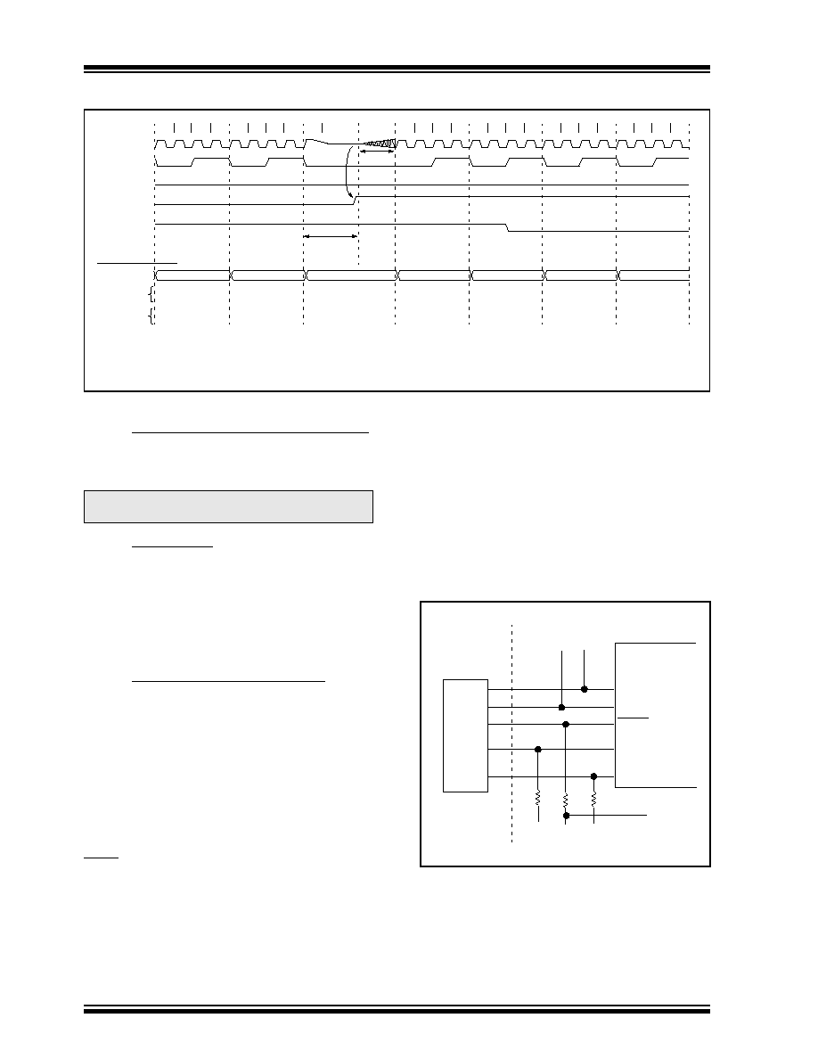
PIC16C9XX
DS30444E - page 118
©
1997 Microchip Technology Inc.
FIGURE 14-18:WAKE-UP FROM SLEEP THROUGH INTERRUPT
Q1
Q2
Q3 Q4
Q1 Q2
Q3
Q4
Q1
Q1
Q2 Q3 Q4
Q1 Q2 Q3 Q4
Q1
Q2 Q3
Q4
Q1 Q2
Q3
Q4
OSC1
CLKOUT(4)
INT pin
INTF flag
(INTCON<1>)
GIE bit
(INTCON<7>)
INSTRUCTION FLOW
PC
Instruction
fetched
Instruction
executed
PC
PC+1
PC+2
Inst(PC) = SLEEP
Inst(PC - 1)
Inst(PC + 1)
SLEEP
Processor in
SLEEP
Interrupt Latency
(Note 2)
Inst(PC + 2)
Inst(PC + 1)
Inst(0004h)
Inst(0005h)
Inst(0004h)
Dummy cycle
PC + 2
0004h
0005h
Dummy cycle
T
OST
(2)
PC+2
Note
1: XT, HS or LP oscillator mode assumed.
2: T
OST
= 1024T
OSC
(drawing not to scale) This delay will not be there for RC osc mode.
3: GIE = '1' assumed. In this case after wake- up, the processor jumps to the interrupt routine. If GIE = '0', execution will continue in-line.
4: CLKOUT is not available in these osc modes, but shown here for timing reference.
14.9
Program Verification/Code Protection
If the code protection bit(s) have not been pro-
grammed, the on-chip program memory can be read
out for verification purposes.
14.10
ID Locations
Four memory locations (2000h - 2003h) are designated
as ID locations where the user can store checksum or
other code-identification numbers. These locations are
not accessible during normal execution but are read-
able and writable during program/verify. It is recom-
mended that only the 4 least significant bits of the ID
location are used.
14.11
In-Circuit Serial Programming
PIC16CXXX microcontrollers can be serially pro-
grammed while in the end application circuit. This is
simply done with two lines for clock and data, and three
other lines for power, ground, and the programming
voltage. This allows customers to manufacture boards
with unprogrammed devices, and then program the
microcontroller just before shipping the product. This
also allows the most recent firmware or a custom firm-
ware to be programmed.
The device is placed into a program/verify mode by
holding the RB6 and RB7 pins low while raising the
MCLR (V
PP
) pin from V
IL
to V
IHH
(see programming
specification). RB6 becomes the programming clock
and RB7 becomes the programming data. Both RB6
and RB7 are Schmitt Trigger inputs in this mode.
Note:
Microchip does not recommend code pro-
tecting windowed devices.
After reset, to place the device into program/verify
mode, the program counter (PC) is at location 00h. A
6-bit command is then supplied to the device. Depend-
ing on the command, 14-bits of program data are then
supplied to or from the device, depending if the com-
mand was a load or a read. For complete details of
serial programming, please refer to the PIC16C6X/7X
Programming Specifications (Literature #DS30228).
FIGURE 14-19:TYPICAL IN-CIRCUIT SERIAL
PROGRAMMING
CONNECTION
External
Connector
Signals
To Normal
Connections
To Normal
Connections
PIC16CXXX
V
DD
V
SS
MCLR/V
PP
RB6
RB7
+5V
0V
V
PP
CLK
Data I/O
V
DD
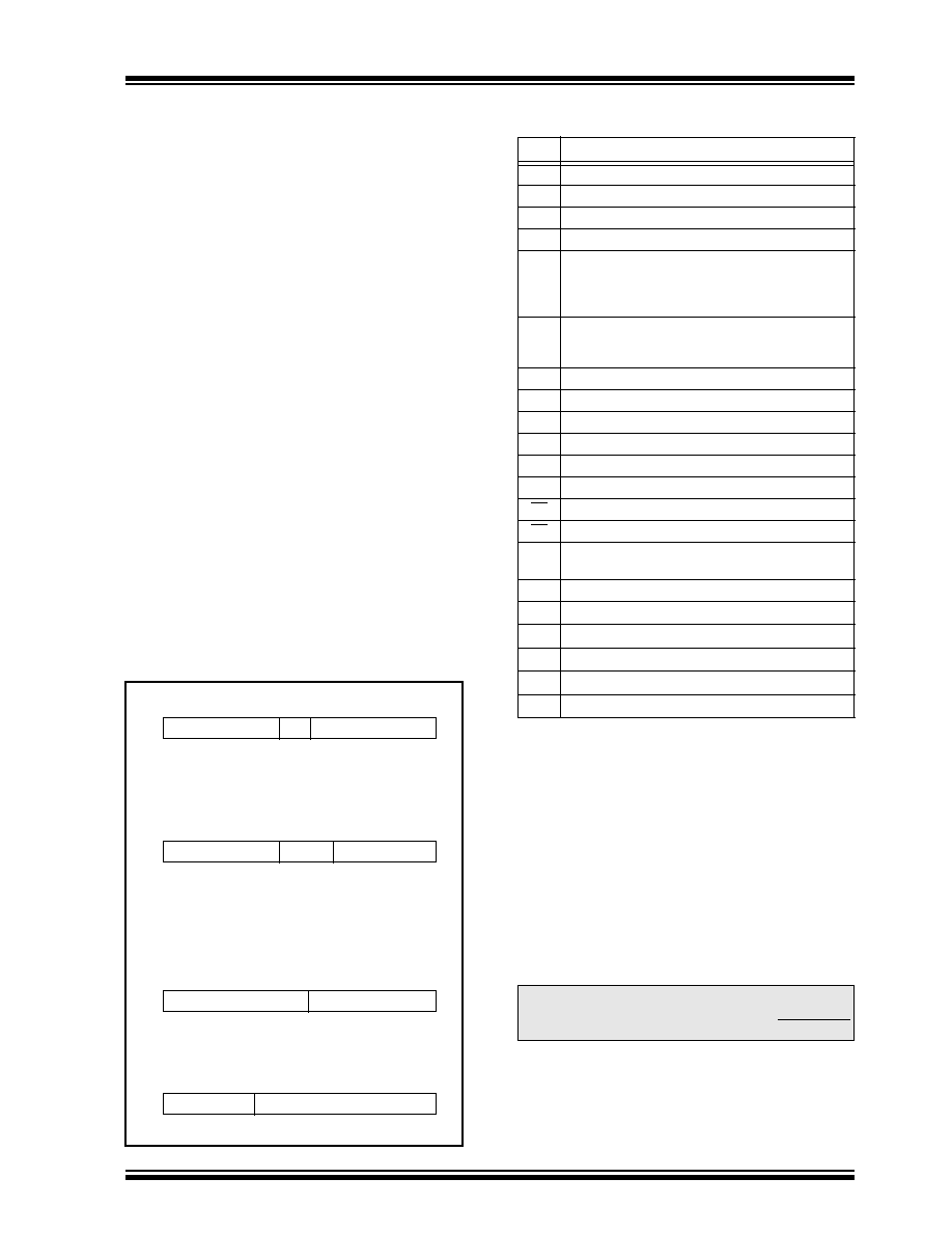
©
1997 Microchip Technology Inc.
DS30444E - page 119
PIC16C9XX
15.0
INSTRUCTION SET SUMMARY
Each PIC16CXXX instruction is a 14-bit word divided
into an OPCODE which specifies the instruction type
and one or more operands which further specify the
operation of the instruction. The PIC16CXX instruction
set summary in Table 15-2 lists byte-oriented, bit-ori-
ented, and literal and control operations. Table 15-1
shows the opcode field descriptions.
For byte-oriented instructions, 'f' represents a file reg-
ister designator and 'd' represents a destination desig-
nator. The file register designator specifies which file
register is to be used by the instruction.
The destination designator specifies where the result of
the operation is to be placed. If 'd' is zero, the result is
placed in the W register. If 'd' is one, the result is placed
in the file register specified in the instruction.
For bit-oriented instructions, 'b' represents a bit field
designator which selects the number of the bit affected
by the operation, while 'f' represents the number of the
file in which the bit is located.
For literal and control operations, 'k' represents an
eight or eleven bit constant or literal value.
The instruction set is highly orthogonal and is grouped
into three basic categories:
· Byte-oriented operations
· Bit-oriented operations
· Literal and control operations
FIGURE 15-1: GENERAL FORMAT FOR
INSTRUCTIONS
Byte-oriented file register operations
13 8 7 6 0
d = 0 for destination W
OPCODE d f (FILE #)
d = 1 for destination f
f = 7-bit file register address
Bit-oriented file register operations
13 10 9 7 6 0
OPCODE b (BIT #) f (FILE #)
b = 3-bit bit address
f = 7-bit file register address
Literal and control operations
13 8 7 0
OPCODE k (literal)
k = 8-bit immediate value
13 11 10 0
OPCODE k (literal)
k = 11-bit immediate value
General
CALL
and
GOTO
instructions only
TABLE 15-1: OPCODE FIELD DESCRIPTIONS
All instructions are executed within one single instruc-
tion cycle, unless a conditional test is true or the pro-
gram counter is changed as a result of an instruction. In
this case, the execution takes two instruction cycles
with the second cycle executed as a NOP. One instruc-
tion cycle consists of four oscillator periods. Thus, for an
oscillator frequency of 4 MHz, the normal instruction
execution time is 1
µ
s. If a conditional test is true or the
program counter is changed as a result of an instruc-
tion, the instruction execution time is 2
µ
s.
Table 15-2 lists the instructions recognized by the
MPASM assembler.
Figure 15-1 shows the general formats that the instruc-
tions can have.
All examples use the following format to represent a
hexadecimal number:
0xhh
where h signifies a hexadecimal digit.
Field
Description
f
Register file address (0x00 to 0x7F)
W
Working register (accumulator)
b
Bit address within an 8-bit file register
k
Literal field, constant data or label
x
Don't care location (= 0 or 1)
The assembler will generate code with x = 0. It is the
recommended form of use for compatibility with all
Microchip software tools.
d
Destination select; d = 0: store result in W,
d = 1: store result in file register f.
Default is d = 1
label
Label name
TOS
Top of Stack
PC
Program Counter
PCLATH
Program Counter High Latch
GIE
Global Interrupt Enable bit
WDT
Watchdog Timer/Counter
TO
Time-out bit
PD
Power-down bit
dest
Destination either the W register or the specified
register file location
[ ]
Options
( )
Contents
Assigned to
< >
Register bit field
In the set of
i
talics User defined term (font is courier)
Note:
To maintain upward compatibility with
future PIC16CXXX products, do not use
the
OPTION
and
TRIS
instructions.

PIC16C9XX
DS30444E - page 120
©
1997 Microchip Technology Inc.
TABLE 15-2: PIC16CXXX INSTRUCTION SET
Mnemonic,
Operands
Description
Cycles
14-Bit Opcode
Status
Affected
Notes
MSb
LSb
BYTE-ORIENTED FILE REGISTER OPERATIONS
ADDWF
ANDWF
CLRF
CLRW
COMF
DECF
DECFSZ
INCF
INCFSZ
IORWF
MOVF
MOVWF
NOP
RLF
RRF
SUBWF
SWAPF
XORWF
f, d
f, d
f
-
f, d
f, d
f, d
f, d
f, d
f, d
f, d
f
-
f, d
f, d
f, d
f, d
f, d
Add W and f
AND W with f
Clear f
Clear W
Complement f
Decrement f
Decrement f, Skip if 0
Increment f
Increment f, Skip if 0
Inclusive OR W with f
Move f
Move W to f
No Operation
Rotate Left f through Carry
Rotate Right f through Carry
Subtract W from f
Swap nibbles in f
Exclusive OR W with f
1
1
1
1
1
1
1(2)
1
1(2)
1
1
1
1
1
1
1
1
1
00
00
00
00
00
00
00
00
00
00
00
00
00
00
00
00
00
00
0111
0101
0001
0001
1001
0011
1011
1010
1111
0100
1000
0000
0000
1101
1100
0010
1110
0110
dfff
dfff
lfff
0xxx
dfff
dfff
dfff
dfff
dfff
dfff
dfff
lfff
0xx0
dfff
dfff
dfff
dfff
dfff
ffff
ffff
ffff
xxxx
ffff
ffff
ffff
ffff
ffff
ffff
ffff
ffff
0000
ffff
ffff
ffff
ffff
ffff
C,DC,Z
Z
Z
Z
Z
Z
Z
Z
Z
C
C
C,DC,Z
Z
1,2
1,2
2
1,2
1,2
1,2,3
1,2
1,2,3
1,2
1,2
1,2
1,2
1,2
1,2
1,2
BIT-ORIENTED FILE REGISTER OPERATIONS
BCF
BSF
BTFSC
BTFSS
f, b
f, b
f, b
f, b
Bit Clear f
Bit Set f
Bit Test f, Skip if Clear
Bit Test f, Skip if Set
1
1
1 (2)
1 (2)
01
01
01
01
00bb
01bb
10bb
11bb
bfff
bfff
bfff
bfff
ffff
ffff
ffff
ffff
1,2
1,2
3
3
LITERAL AND CONTROL OPERATIONS
ADDLW
ANDLW
CALL
CLRWDT
GOTO
IORLW
MOVLW
RETFIE
RETLW
RETURN
SLEEP
SUBLW
XORLW
k
k
k
-
k
k
k
-
k
-
-
k
k
Add literal and W
AND literal with W
Call subroutine
Clear Watchdog Timer
Go to address
Inclusive OR literal with W
Move literal to W
Return from interrupt
Return with literal in W
Return from Subroutine
Go into standby mode
Subtract W from literal
Exclusive OR literal with W
1
1
2
1
2
1
1
2
2
2
1
1
1
11
11
10
00
10
11
11
00
11
00
00
11
11
111x
1001
0kkk
0000
1kkk
1000
00xx
0000
01xx
0000
0000
110x
1010
kkkk
kkkk
kkkk
0110
kkkk
kkkk
kkkk
0000
kkkk
0000
0110
kkkk
kkkk
kkkk
kkkk
kkkk
0100
kkkk
kkkk
kkkk
1001
kkkk
1000
0011
kkkk
kkkk
C,DC,Z
Z
TO
,
PD
Z
TO
,
PD
C,DC,Z
Z
Note
1: When an I/O register is modified as a function of itself ( e.g.,
MOVF PORTB, 1
), the value used will be that value present
on the pins themselves. For example, if the data latch is '1' for a pin configured as input and is driven low by an external
device, the data will be written back with a '0'.
2: If this instruction is executed on the TMR0 register (and, where applicable, d = 1), the prescaler will be cleared if assigned
to the Timer0 Module.
3: If Program Counter (PC) is modified or a conditional test is true, the instruction requires two cycles. The second cycle is
executed as a NOP.
©
1997 Microchip Technology Inc.
DS30444E - page 121
PIC16C9XX
15.1
Instruction Descriptions
ADDLW
Add Literal and W
Syntax:
[
label] ADDLW k
Operands:
0
k
255
Operation:
(W) + k
(W)
Status Affected:
C, DC, Z
Encoding:
11
111x
kkkk
kkkk
Description:
The contents of the W register are
added to the eight bit literal 'k' and the
result is placed in the W register
.
Words:
1
Cycles:
1
Q Cycle Activity:
Q1
Q2
Q3
Q4
Decode
Read
literal 'k'
Process
data
Write to
W
Example:
ADDLW
0x15
Before Instruction
W
=
0x10
After Instruction
W
=
0x25
ADDWF
Add W and f
Syntax:
[
label] ADDWF f,d
Operands:
0
f
127
d
[0,1]
Operation:
(W) + (f)
(destination)
Status Affected:
C, DC, Z
Encoding:
00
0111
dfff
ffff
Description:
Add the contents of the W register with
register 'f'. If 'd' is 0 the result is stored
in the W register. If 'd' is 1 the result is
stored back in register 'f'
.
Words:
1
Cycles:
1
Q Cycle Activity:
Q1
Q2
Q3
Q4
Decode
Read
register
'f'
Process
data
Write to
destination
Example
ADDWF
FSR,
0
Before Instruction
W
=
0x17
FSR =
0xC2
After Instruction
W
=
0xD9
FSR =
0xC2
PIC16C9XX
DS30444E - page 122
©
1997 Microchip Technology Inc.
ANDLW
AND Literal with W
Syntax:
[
label] ANDLW k
Operands:
0
k
255
Operation:
(W) .AND. (k)
(W)
Status Affected:
Z
Encoding:
11
1001
kkkk
kkkk
Description:
The contents of W register are
AND'ed with the eight bit literal 'k'. The
result is placed in the W register
.
Words:
1
Cycles:
1
Q Cycle Activity:
Q1
Q2
Q3
Q4
Decode
Read
literal "k"
Process
data
Write to
W
Example
ANDLW
0x5F
Before Instruction
W
=
0xA3
After Instruction
W
=
0x03
ANDWF
AND W with f
Syntax:
[
label] ANDWF f,d
Operands:
0
f
127
d
[0,1]
Operation:
(W) .AND. (f)
(destination)
Status Affected:
Z
Encoding:
00
0101
dfff
ffff
Description:
AND the W register with register 'f'. If 'd'
is 0 the result is stored in the W regis-
ter. If 'd' is 1 the result is stored back in
register 'f'
.
Words:
1
Cycles:
1
Q Cycle Activity:
Q1
Q2
Q3
Q4
Decode
Read
register
'f'
Process
data
Write to
destination
Example
ANDWF
FSR,
1
Before Instruction
W
=
0x17
FSR =
0xC2
After Instruction
W
=
0x17
FSR =
0x02
BCF
Bit Clear f
Syntax:
[
label] BCF f,b
Operands:
0
f
127
0
b
7
Operation:
0
(f<b>)
Status Affected:
None
Encoding:
01
00bb
bfff
ffff
Description:
Bit 'b' in register 'f' is cleared
.
Words:
1
Cycles:
1
Q Cycle Activity:
Q1
Q2
Q3
Q4
Decode
Read
register
'f'
Process
data
Write
register 'f'
Example
BCF
FLAG_REG, 7
Before Instruction
FLAG_REG = 0xC7
After Instruction
FLAG_REG = 0x47
©
1997 Microchip Technology Inc.
DS30444E - page 123
PIC16C9XX
BSF
Bit Set f
Syntax:
[
label] BSF f,b
Operands:
0
f
127
0
b
7
Operation:
1
(f<b>)
Status Affected:
None
Encoding:
01
01bb
bfff
ffff
Description:
Bit 'b' in register 'f' is set.
Words:
1
Cycles:
1
Q Cycle Activity:
Q1
Q2
Q3
Q4
Decode
Read
register
'f'
Process
data
Write
register 'f'
Example
BSF
FLAG_REG, 7
Before Instruction
FLAG_REG = 0x0A
After Instruction
FLAG_REG = 0x8A
BTFSC
Bit Test, Skip if Clear
Syntax:
[
label] BTFSC f,b
Operands:
0
f
127
0
b
7
Operation:
skip if (f<b>) = 0
Status Affected:
None
Encoding:
01
10bb
bfff
ffff
Description:
If bit 'b' in register 'f' is '1' then the next
instruction is executed.
If bit 'b', in register 'f', is '0' then the next
instruction is discarded, and a NOP is
executed instead, making this a 2T
CY
instruction
.
Words:
1
Cycles:
1(2)
Q Cycle Activity:
Q1
Q2
Q3
Q4
Decode
Read
register 'f'
Process
data
No-
Operation
If Skip:
(2nd Cycle)
Q1
Q2
Q3
Q4
No-
Operation
No-
Operation
No-
Operation
No-
Operation
Example
HERE
FALSE
TRUE
BTFSC
GOTO
·
·
·
FLAG,1
PROCESS_CODE
Before Instruction
PC =
address
HERE
After Instruction
if FLAG<1> = 0,
PC = address
TRUE
if FLAG<1>=1,
PC = address
FALSE
PIC16C9XX
DS30444E - page 124
©
1997 Microchip Technology Inc.
BTFSS
Bit Test f, Skip if Set
Syntax:
[
label] BTFSS f,b
Operands:
0
f
127
0
b < 7
Operation:
skip if (f<b>) = 1
Status Affected:
None
Encoding:
01
11bb
bfff
ffff
Description:
If bit 'b' in register 'f' is '0' then the next
instruction is executed.
If bit 'b' is '1', then the next instruction is
discarded and a NOP is executed
instead, making this a 2T
CY
instruction.
Words:
1
Cycles:
1(2)
Q Cycle Activity:
Q1
Q2
Q3
Q4
Decode
Read
register 'f'
Process
data
No-
Operation
If Skip:
(2nd Cycle)
Q1
Q2
Q3
Q4
No-
Operation
No-
Operation
No-
Operation
No-
Operation
Example
HERE
FALSE
TRUE
BTFSC
GOTO
·
·
·
FLAG,1
PROCESS_CODE
Before Instruction
PC =
address
HERE
After Instruction
if FLAG<1> = 0,
PC = address
FALSE
if FLAG<1> = 1,
PC = address
TRUE
CALL
Call Subroutine
Syntax:
[
label ] CALL k
Operands:
0
k
2047
Operation:
(PC)+ 1
TOS,
k
PC<10:0>,
(PCLATH<4:3>)
PC<12:11>
Status Affected:
None
Encoding:
10
0kkk
kkkk
kkkk
Description:
Call Subroutine. First, return address
(PC+1) is pushed onto the stack. The
eleven bit immediate address is loaded
into PC bits <10:0>. The upper bits of
the PC are loaded from PCLATH.
CALL
is a two cycle instruction.
Words:
1
Cycles:
2
Q Cycle Activity:
Q1
Q2
Q3
Q4
1st Cycle
Decode
Read
literal 'k',
Push PC
to Stack
Process
data
Write to
PC
2nd Cycle
No-
Operation
No-
Operation
No-
Operation
No-
Operation
Example
HERE
CALL THERE
Before Instruction
PC = Address
HERE
After Instruction
PC = Address
THERE
TOS = Address
HERE+1
©
1997 Microchip Technology Inc.
DS30444E - page 125
PIC16C9XX
CLRF
Clear f
Syntax:
[
label] CLRF f
Operands:
0
f
127
Operation:
00h
(f)
1
Z
Status Affected:
Z
Encoding:
00
0001
1fff
ffff
Description:
The contents of register 'f' are cleared
and the Z bit is set.
Words:
1
Cycles:
1
Q Cycle Activity:
Q1
Q2
Q3
Q4
Decode
Read
register
'f'
Process
data
Write
register 'f'
Example
CLRF
FLAG_REG
Before Instruction
FLAG_REG
=
0x5A
After Instruction
FLAG_REG
=
0x00
Z
=
1
CLRW
Clear W
Syntax:
[
label ] CLRW
Operands:
None
Operation:
00h
(W)
1
Z
Status Affected:
Z
Encoding:
00
0001
0xxx
xxxx
Description:
W register is cleared. Zero bit (Z) is
set.
Words:
1
Cycles:
1
Q Cycle Activity:
Q1
Q2
Q3
Q4
Decode
No-
Operation
Process
data
Write to
W
Example
CLRW
Before Instruction
W
=
0x5A
After Instruction
W
=
0x00
Z
=
1
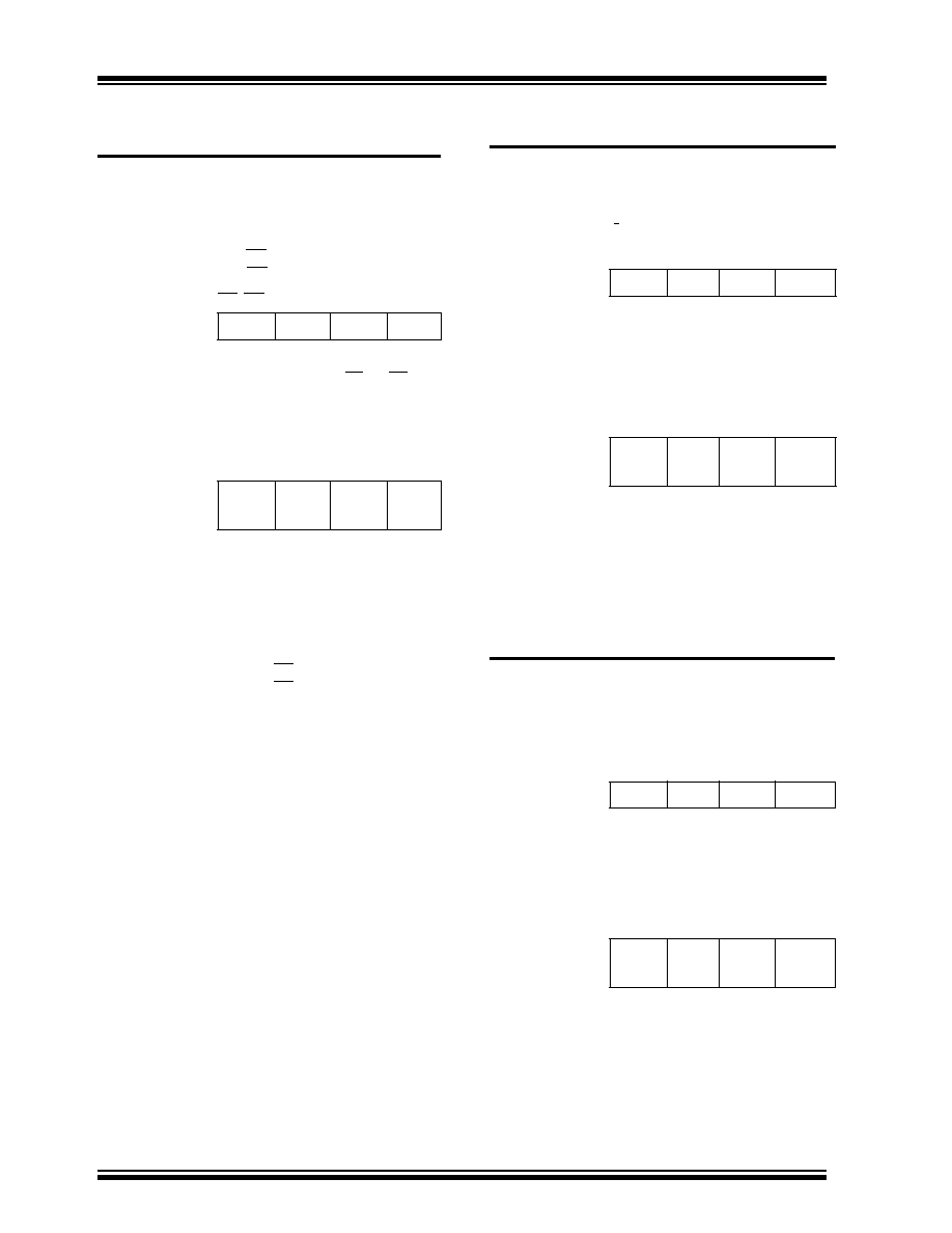
PIC16C9XX
DS30444E - page 126
©
1997 Microchip Technology Inc.
CLRWDT
Clear Watchdog Timer
Syntax:
[
label ] CLRWDT
Operands:
None
Operation:
00h
WDT
0
WDT prescaler,
1
TO
1
PD
Status Affected:
TO, PD
Encoding:
00
0000
0110
0100
Description:
CLRWDT
instruction resets the Watch-
dog Timer. It also resets the prescaler
of the WDT. Status bits TO and PD are
set.
Words:
1
Cycles:
1
Q Cycle Activity:
Q1
Q2
Q3
Q4
Decode
No-
Operation
Process
data
Clear
WDT
Counter
Example
CLRWDT
Before Instruction
WDT counter =
?
After Instruction
WDT counter =
0x00
WDT prescaler=
0
TO
=
1
PD
=
1
COMF
Complement f
Syntax:
[
label ] COMF f,d
Operands:
0
f
127
d
[0,1]
Operation:
(f)
(destination)
Status Affected:
Z
Encoding:
00
1001
dfff
ffff
Description:
The contents of register 'f' are comple-
mented. If 'd' is 0 the result is stored in
W. If 'd' is 1 the result is stored back in
register 'f'.
Words:
1
Cycles:
1
Q Cycle Activity:
Q1
Q2
Q3
Q4
Decode
Read
register
'f'
Process
data
Write to
destination
Example
COMF
REG1,0
Before Instruction
REG1
=
0x13
After Instruction
REG1
=
0x13
W
=
0xEC
DECF
Decrement f
Syntax:
[
label] DECF f,d
Operands:
0
f
127
d
[0,1]
Operation:
(f) - 1
(destination)
Status Affected:
Z
Encoding:
00
0011
dfff
ffff
Description:
Decrement register 'f'. If 'd' is 0 the
result is stored in the W register. If 'd' is
1 the result is stored back in register 'f'
.
Words:
1
Cycles:
1
Q Cycle Activity:
Q1
Q2
Q3
Q4
Decode
Read
register
'f'
Process
data
Write to
destination
Example
DECF CNT, 1
Before Instruction
CNT
=
0x01
Z
=
0
After Instruction
CNT
=
0x00
Z
=
1
©
1997 Microchip Technology Inc.
DS30444E - page 127
PIC16C9XX
DECFSZ
Decrement f, Skip if 0
Syntax:
[
label ] DECFSZ f,d
Operands:
0
f
127
d
[0,1]
Operation:
(f) - 1
(destination);
skip if result = 0
Status Affected:
None
Encoding:
00
1011
dfff
ffff
Description:
The contents of register 'f' are decre-
mented. If 'd' is 0 the result is placed in the
W register. If 'd' is 1 the result is placed
back in register 'f'.
If the result is 1, the next instruction, is
executed. If the result is 0, then a NOP is
executed instead making it a 2T
CY
instruc-
tion.
Words:
1
Cycles:
1(2)
Q Cycle Activity:
Q1
Q2
Q3
Q4
Decode
Read
register 'f'
Process
data
Write to
destination
If Skip:
(2nd Cycle)
Q1
Q2
Q3
Q4
No-
Operation
No-
Operation
No-
Operation
No-
Operation
Example
HERE DECFSZ CNT, 1
GOTO LOOP
CONTINUE
·
·
·
Before Instruction
PC
=
address
HERE
After Instruction
CNT
=
CNT - 1
if CNT =
0,
PC
=
address
CONTINUE
if CNT
0,
PC
=
address
HERE+1
GOTO
Unconditional Branch
Syntax:
[
label ] GOTO k
Operands:
0
k
2047
Operation:
k
PC<10:0>
PCLATH<4:3>
PC<12:11>
Status Affected:
None
Encoding:
10
1kkk
kkkk
kkkk
Description:
GOTO
is an unconditional branch. The
eleven bit immediate value is loaded
into PC bits <10:0>. The upper bits of
PC are loaded from PCLATH<4:3>.
GOTO
is a two cycle instruction.
Words:
1
Cycles:
2
Q Cycle Activity:
Q1
Q2
Q3
Q4
1st Cycle
Decode
Read
literal 'k'
Process
data
Write to
PC
2nd Cycle
No-
Operation
No-
Operation
No-
Operation
No-
Operation
Example
GOTO THERE
After Instruction
PC =
Address
THERE
PIC16C9XX
DS30444E - page 128
©
1997 Microchip Technology Inc.
INCF
Increment f
Syntax:
[
label ] INCF f,d
Operands:
0
f
127
d
[0,1]
Operation:
(f) + 1
(destination)
Status Affected:
Z
Encoding:
00
1010
dfff
ffff
Description:
The contents of register 'f' are incre-
mented. If 'd' is 0 the result is placed in
the W register. If 'd' is 1 the result is
placed back in register 'f'.
Words:
1
Cycles:
1
Q Cycle Activity:
Q1
Q2
Q3
Q4
Decode
Read
register
'f'
Process
data
Write to
destination
Example
INCF
CNT,
1
Before Instruction
CNT
=
0xFF
Z
=
0
After Instruction
CNT
=
0x00
Z
=
1
INCFSZ
Increment f, Skip if 0
Syntax:
[
label ] INCFSZ f,d
Operands:
0
f
127
d
[0,1]
Operation:
(f) + 1
(destination),
skip if result = 0
Status Affected:
None
Encoding:
00
1111
dfff
ffff
Description:
The contents of register 'f' are incre-
mented. If 'd' is 0 the result is placed in
the W register. If 'd' is 1 the result is
placed back in register 'f'.
If the result is 1, the next instruction is
executed. If the result is 0, a NOP is
executed instead making it a 2T
CY
instruction
.
Words:
1
Cycles:
1(2)
Q Cycle Activity:
Q1
Q2
Q3
Q4
Decode
Read
register 'f'
Process
data
Write to
destination
If Skip:
(2nd Cycle)
Q1
Q2
Q3
Q4
No-
Operation
No-
Operation
No-
Operation
No-
Operation
Example
HERE INCFSZ CNT, 1
GOTO LOOP
CONTINUE
·
·
·
Before Instruction
PC
=
address
HERE
After Instruction
CNT
=
CNT + 1
if CNT=
0,
PC
=
address
CONTINUE
if CNT
0,
PC
=
address
HERE +1
©
1997 Microchip Technology Inc.
DS30444E - page 129
PIC16C9XX
IORLW
Inclusive OR Literal with W
Syntax:
[
label ] IORLW k
Operands:
0
k
255
Operation:
(W) .OR. k
(W)
Status Affected:
Z
Encoding:
11
1000
kkkk
kkkk
Description:
The contents of the W register is
OR'ed with the eight bit literal 'k'. The
result is placed in the W register
.
Words:
1
Cycles:
1
Q Cycle Activity:
Q1
Q2
Q3
Q4
Decode
Read
literal 'k'
Process
data
Write to
W
Example
IORLW
0x35
Before Instruction
W
=
0x9A
After Instruction
W
=
0xBF
Z
=
1
IORWF
Inclusive OR W with f
Syntax:
[
label ] IORWF f,d
Operands:
0
f
127
d
[0,1]
Operation:
(W) .OR. (f)
(destination)
Status Affected:
Z
Encoding:
00
0100
dfff
ffff
Description:
Inclusive OR the W register with regis-
ter 'f'. If 'd' is 0 the result is placed in the
W register. If 'd' is 1 the result is placed
back in register 'f'.
Words:
1
Cycles:
1
Q Cycle Activity:
Q1
Q2
Q3
Q4
Decode
Read
register
'f'
Process
data
Write to
destination
Example
IORWF
RESULT, 0
Before Instruction
RESULT =
0x13
W
=
0x91
After Instruction
RESULT =
0x13
W
=
0x93
Z
=
1
PIC16C9XX
DS30444E - page 130
©
1997 Microchip Technology Inc.
MOVF
Move f
Syntax:
[
label ] MOVF f,d
Operands:
0
f
127
d
[0,1]
Operation:
(f)
(destination)
Status Affected:
Z
Encoding:
00
1000
dfff
ffff
Description:
The contents of register f is moved to a
destination dependant upon the status
of d. If d = 0, destination is W register. If
d = 1, the destination is file register f
itself. d = 1 is useful to test a file regis-
ter since status flag Z is affected.
Words:
1
Cycles:
1
Q Cycle Activity:
Q1
Q2
Q3
Q4
Decode
Read
register
'f'
Process
data
Write to
destination
Example
MOVF
FSR,
0
After Instruction
W = value in FSR register
Z
= 1
MOVLW
Move Literal to W
Syntax:
[
label ] MOVLW k
Operands:
0
k
255
Operation:
k
(W)
Status Affected:
None
Encoding:
11
00xx
kkkk
kkkk
Description:
The eight bit literal 'k' is loaded into W
register
.
The don't cares will assemble
as 0's.
Words:
1
Cycles:
1
Q Cycle Activity:
Q1
Q2
Q3
Q4
Decode
Read
literal 'k'
Process
data
Write to
W
Example
MOVLW
0x5A
After Instruction
W
=
0x5A
MOVWF
Move W to f
Syntax:
[
label ] MOVWF f
Operands:
0
f
127
Operation:
(W)
(f)
Status Affected:
None
Encoding:
00
0000
1fff
ffff
Description:
Move data from W register to register
'f'
.
Words:
1
Cycles:
1
Q Cycle Activity:
Q1
Q2
Q3
Q4
Decode
Read
register
'f'
Process
data
Write
register 'f'
Example
MOVWF
OPTION_REG
Before Instruction
OPTION =
0xFF
W
=
0x4F
After Instruction
OPTION =
0x4F
W
=
0x4F
©
1997 Microchip Technology Inc.
DS30444E - page 131
PIC16C9XX
NOP
No Operation
Syntax:
[
label ] NOP
Operands:
None
Operation:
No operation
Status Affected:
None
Encoding:
00
0000
0xx0
0000
Description:
No operation.
Words:
1
Cycles:
1
Q Cycle Activity:
Q1
Q2
Q3
Q4
Decode
No-
Operation
No-
Operation
No-
Operation
Example
NOP
OPTION
Load Option Register
Syntax:
[
label ] OPTION
Operands:
None
Operation:
(W)
OPTION
Status Affected: None
Encoding:
00
0000
0110
0010
Description:
The contents of the W register are
loaded in the OPTION register. This
instruction is supported for code com-
patibility with PIC16C5X products.
Since OPTION is a readable/writable
register, the user can directly address
it.
Words:
1
Cycles:
1
Example
To maintain upward compatibility
with future PIC16CXX products, do
not use this instruction.
RETFIE
Return from Interrupt
Syntax:
[
label ] RETFIE
Operands:
None
Operation:
TOS
PC,
1
GIE
Status Affected:
None
Encoding:
00
0000
0000
1001
Description:
Return from Interrupt. Stack is POPed
and Top of Stack (TOS) is loaded in the
PC. Interrupts are enabled by setting
Global Interrupt Enable bit, GIE
(INTCON<7>). This is a two cycle
instruction.
Words:
1
Cycles:
2
Q Cycle Activity:
Q1
Q2
Q3
Q4
1st Cycle
Decode
No-
Operation
Set the
GIE bit
Pop from
the Stack
2nd Cycle
No-
Operation
No-
Operation
No-
Operation
No-
Operation
Example
RETFIE
After Interrupt
PC =
TOS
GIE =
1
PIC16C9XX
DS30444E - page 132
©
1997 Microchip Technology Inc.
RETLW
Return with Literal in W
Syntax:
[
label ] RETLW k
Operands:
0
k
255
Operation:
k
(W);
TOS
PC
Status Affected:
None
Encoding:
11
01xx
kkkk
kkkk
Description:
The W register is loaded with the eight
bit literal 'k'. The program counter is
loaded from the top of the stack (the
return address). This is a two cycle
instruction.
Words:
1
Cycles:
2
Q Cycle Activity:
Q1
Q2
Q3
Q4
1st Cycle
Decode
Read
literal 'k'
No-
Operation
Write to W,
Pop from
the Stack
2nd Cycle
No-
Operation
No-
Operation
No-
Operation
No-
Operation
Example
TABLE
CALL TABLE ;W contains table
;offset value
·
;W now has table value
·
·
ADDWF PC ;W = offset
RETLW k1 ;Begin table
RETLW k2 ;
·
·
·
RETLW kn ; End of table
Before Instruction
W
=
0x07
After Instruction
W
=
value of k8
RETURN
Return from Subroutine
Syntax:
[
label ] RETURN
Operands:
None
Operation:
TOS
PC
Status Affected:
None
Encoding:
00
0000
0000
1000
Description:
Return from subroutine. The stack is
POPed and the top of the stack (TOS)
is loaded into the program counter. This
is a two cycle instruction.
Words:
1
Cycles:
2
Q Cycle Activity:
Q1
Q2
Q3
Q4
1st Cycle
Decode
No-
Operation
No-
Operation
Pop from
the Stack
2nd Cycle
No-
Operation
No-
Operation
No-
Operation
No-
Operation
Example
RETURN
After Interrupt
PC =
TOS
©
1997 Microchip Technology Inc.
DS30444E - page 133
PIC16C9XX
RLF
Rotate Left f through Carry
Syntax:
[
label ]
RLF f,d
Operands:
0
f
127
d
[0,1]
Operation:
See description below
Status Affected:
C
Encoding:
00
1101
dfff
ffff
Description:
The contents of register 'f' are rotated
one bit to the left through the Carry
Flag. If 'd' is 0 the result is placed in the
W register. If 'd' is 1 the result is stored
back in register 'f'.
Words:
1
Cycles:
1
Q Cycle Activity:
Q1
Q2
Q3
Q4
Decode
Read
register
'f'
Process
data
Write to
destination
Example
RLF
REG1,0
Before Instruction
REG1
=
1110 0110
C
=
0
After Instruction
REG1
=
1110 0110
W
=
1100 1100
C
=
1
Register f
C
RRF
Rotate Right f through Carry
Syntax:
[
label ] RRF f,d
Operands:
0
f
127
d
[0,1]
Operation:
See description below
Status Affected:
C
Encoding:
00
1100
dfff
ffff
Description:
The contents of register 'f' are rotated
one bit to the right through the Carry
Flag. If 'd' is 0 the result is placed in the
W register. If 'd' is 1 the result is placed
back in register 'f'.
Words:
1
Cycles:
1
Q Cycle Activity:
Q1
Q2
Q3
Q4
Decode
Read
register
'f'
Process
data
Write to
destination
Example
RRF
REG1,0
Before Instruction
REG1
=
1110 0110
C
=
0
After Instruction
REG1
=
1110 0110
W
=
0111 0011
C
=
0
Register f
C
PIC16C9XX
DS30444E - page 134
©
1997 Microchip Technology Inc.
SLEEP
Syntax:
[
label ]
SLEEP
Operands:
None
Operation:
00h
WDT,
0
WDT prescaler,
1
TO,
0
PD
Status Affected:
TO, PD
Encoding:
00
0000
0110
0011
Description:
The power-down status bit, PD is
cleared. Time-out status bit, TO is
set. Watchdog Timer and its pres-
caler are cleared.
The processor is put into SLEEP
mode with the oscillator stopped. See
Section 14.8 for more details.
Words:
1
Cycles:
1
Q Cycle Activity:
Q1
Q2
Q3
Q4
Decode
No-
Operation
No-
Operation
Go to
Sleep
Example:
SLEEP
SUBLW
Subtract W from Literal
Syntax:
[
label ]
SUBLW k
Operands:
0
k
255
Operation:
k - (W)
(
W)
Status Affected:
C, DC, Z
Encoding:
11
110x
kkkk
kkkk
Description:
The W register is subtracted (2's comple-
ment method) from the eight bit literal 'k'.
The result is placed in the W register.
Words:
1
Cycles:
1
Q Cycle Activity:
Q1
Q2
Q3
Q4
Decode
Read
literal 'k'
Process
data
Write to W
Example 1:
SUBLW
0x02
Before Instruction
W
=
1
C
=
?
Z
=
?
After Instruction
W
=
1
C
=
1; result is positive
Z
=
0
Example 2:
Before Instruction
W
=
2
C
=
?
Z
=
?
After Instruction
W
=
0
C
=
1; result is zero
Z
=
1
Example 3:
Before Instruction
W
=
3
C
=
?
Z
=
?
After Instruction
W
=
0xFF
C
=
0; result is nega-
tive
Z
=
0
©
1997 Microchip Technology Inc.
DS30444E - page 135
PIC16C9XX
SUBWF
Subtract W from f
Syntax:
[
label ]
SUBWF f,d
Operands:
0
f
127
d
[0,1]
Operation:
(f) - (W)
(
destination)
Status Affected:
C, DC, Z
Encoding:
00
0010
dfff
ffff
Description:
Subtract (2's complement method) W reg-
ister from register 'f'. If 'd' is 0 the result is
stored in the W register. If 'd' is 1 the
result is stored back in register 'f'.
Words:
1
Cycles:
1
Q Cycle Activity:
Q1
Q2
Q3
Q4
Decode
Read
register 'f'
Process
data
Write to
destination
Example 1:
SUBWF
REG1,
1
Before Instruction
REG1
=
3
W
=
2
C
=
?
Z
=
?
After Instruction
REG1
=
1
W
=
2
C
=
1; result is positive
Z
=
0
Example 2:
Before Instruction
REG1
=
2
W
=
2
C
=
?
Z
=
?
After Instruction
REG1
=
0
W
=
2
C
=
1; result is zero
Z
=
1
Example 3:
Before Instruction
REG1
=
1
W
=
2
C
=
?
Z
=
?
After Instruction
REG1
=
0xFF
W
=
2
C
=
0; result is negative
Z
=
0
SWAPF
Swap Nibbles in f
Syntax:
[
label ] SWAPF f,d
Operands:
0
f
127
d
[0,1]
Operation:
(f<3:0>)
(destination<7:4>),
(f<7:4>)
(destination<3:0>)
Status Affected:
None
Encoding:
00
1110
dfff
ffff
Description:
The upper and lower nibbles of register
'f' are exchanged. If 'd' is 0 the result is
placed in W register. If 'd' is 1 the result
is placed in register 'f'.
Words:
1
Cycles:
1
Q Cycle Activity:
Q1
Q2
Q3
Q4
Decode
Read
register 'f'
Process
data
Write to
destination
Example
SWAPF
REG,
0
Before Instruction
REG1
=
0xA5
After Instruction
REG1
=
0xA5
W
=
0x5A
TRIS
Load TRIS Register
Syntax:
[
label]
TRIS
f
Operands:
5
f
7
Operation:
(W)
TRIS register f;
Status Affected: None
Encoding:
00
0000
0110
0fff
Description:
The instruction is supported for code
compatibility with the PIC16C5X prod-
ucts. Since TRIS registers are read-
able and writable, the user can directly
address them.
Words:
1
Cycles:
1
Example
To maintain upward compatibility
with future PIC16CXX products, do
not use this instruction.
PIC16C9XX
DS30444E - page 136
©
1997 Microchip Technology Inc.
XORLW
Exclusive OR Literal with W
Syntax:
[
label]
XORLW k
Operands:
0
k
255
Operation:
(W) .XOR. k
(
W)
Status Affected:
Z
Encoding:
11
1010
kkkk
kkkk
Description:
The contents of the W register are
XOR'ed with the eight bit literal 'k'.
The result is placed in the W regis-
ter.
Words:
1
Cycles:
1
Q Cycle Activity:
Q1
Q2
Q3
Q4
Decode
Read
literal 'k'
Process
data
Write to
W
Example:
XORLW
0xAF
Before Instruction
W
=
0xB5
After Instruction
W
=
0x1A
XORWF
Exclusive OR W with f
Syntax:
[
label]
XORWF f,d
Operands:
0
f
127
d
[0,1]
Operation:
(W) .XOR. (f)
(
destination)
Status Affected:
Z
Encoding:
00
0110
dfff
ffff
Description:
Exclusive OR the contents of the W
register with register 'f'. If 'd' is 0 the
result is stored in the W register. If 'd' is
1 the result is stored back in register 'f'.
Words:
1
Cycles:
1
Q Cycle Activity:
Q1
Q2
Q3
Q4
Decode
Read
register
'f'
Process
data
Write to
destination
Example
XORWF
REG
1
Before Instruction
REG
=
0xAF
W
=
0xB5
After Instruction
REG
=
0x1A
W
=
0xB5

©
1997 Microchip Technology Inc.
DS30444E - page 137
PIC16C9XX
16.0
DEVELOPMENT SUPPORT
16.1
Development Tools
The PICmicr
TM
microcontrollers are supported with a
full range of hardware and software development tools:
· PICMASTER/PICMASTER CE
Real-Time
In-Circuit Emulator
· ICEPIC Low-Cost PIC16C5X and PIC16CXXX
In-Circuit Emulator
· PRO MATE
®
II Universal Programmer
· PICSTART
®
Plus Entry-Level Prototype
Programmer
· PICDEM-1 Low-Cost Demonstration Board
· PICDEM-2 Low-Cost Demonstration Board
· PICDEM-3 Low-Cost Demonstration Board
· MPASM Assembler
· MPLAB
TM
SIM Software Simulator
· MPLAB-C (C Compiler)
· Fuzzy Logic Development System
(
fuzzyTECH
®
-
MP)
16.2
PICMASTER: High Performance
Universal In-Circuit Emulator with
MPLAB IDE
The PICMASTER Universal In-Circuit Emulator is
intended to provide the product development engineer
with a complete microcontroller design tool set for all
microcontrollers in the PIC12CXXX, PIC14C000,
PIC16C5X, PIC16CXXX and PIC17CXX families.
PICMASTER is supplied with the MPLAB
TM
Integrated
Development Environment (IDE), which allows editing,
"make" and download, and source debugging from a
single environment.
Interchangeable target probes allow the system to be
easily reconfigured for emulation of different proces-
sors. The universal architecture of the PICMASTER
allows expansion to support all new Microchip micro-
controllers.
The PICMASTER Emulator System has been designed
as a real-time emulation system with advanced fea-
tures that are generally found on more expensive devel-
opment tools. The PC compatible 386 (and higher)
machine platform and Microsoft Windows
®
3.x environ-
ment were chosen to best make these features avail-
able to you, the end user.
A CE compliant version of PICMASTER is available for
European Union (EU) countries.
16.3
ICEPIC: Low-Cost PIC16CXXX
In-Circuit Emulator
ICEPIC is a low-cost in-circuit emulator solution for the
Microchip PIC16C5X and PIC16CXXX families of 8-bit
OTP microcontrollers.
ICEPIC is designed to operate on PC-compatible
machines ranging from 286-AT
®
through Pentium
TM
based machines under Windows 3.x environment.
ICEPIC features real time, non-intrusive emulation.
16.4
PRO MATE II: Universal Programmer
The PRO MATE II Universal Programmer is a full-fea-
tured programmer capable of operating in stand-alone
mode as well as PC-hosted mode.
The PRO MATE II has programmable V
DD
and V
PP
supplies which allows it to verify programmed memory
at V
DD
min and V
DD
max for maximum reliability. It has
an LCD display for displaying error messages, keys to
enter commands and a modular detachable socket
assembly to support various package types. In stand-
alone mode the PRO MATE II can read, verify or pro-
gram
PIC12CXXX, PIC14C000, PIC16C5X,
PIC16CXXX and PIC17CXX devices. It can also set
configuration and code-protect bits in this mode.
16.5
PICSTART Plus Entry Level
Development System
The PICSTART programmer is an easy-to-use, low-
cost prototype programmer. It connects to the PC via
one of the COM (RS-232) ports. MPLAB Integrated
Development Environment software makes using the
programmer simple and efficient. PICSTART Plus is not
recommended for production programming.
PICSTART Plus supports all PIC12CXXX, PIC14C000,
PIC16C5X, PIC16CXXX and PIC17CXX devices with
up to 40 pins. Larger pin count devices such as the
PIC16C923 and PIC16C924 may be supported with an
adapter socket.

PIC16C9XX
DS30444E - page 138
©
1997 Microchip Technology Inc.
16.6
PICDEM-1 Low-Cost PICmicro
Demonstration Board
The PICDEM-1 is a simple board which demonstrates
the capabilities of several of Microchip's microcontrol-
lers. The microcontrollers supported are: PIC16C5X
(PIC16C54 to PIC16C58A), PIC16C61, PIC16C62X,
PIC16C71, PIC16C8X, PIC17C42, PIC17C43 and
PIC17C44. All necessary hardware and software is
included to run basic demo programs. The users can
program the sample microcontrollers provided with
the PICDEM-1 board, on a PRO
MATE II or
PICSTART-Plus programmer, and easily test firm-
ware. The user can also connect the PICDEM-1
board to the PICMASTER emulator and download
the firmware to the emulator for testing. Additional pro-
totype area is available for the user to build some addi-
tional hardware and connect it to the microcontroller
socket(s). Some of the features include an RS-232
interface, a potentiometer for simulated analog input,
push-button switches and eight LEDs connected to
PORTB.
16.7
PICDEM-2 Low-Cost PIC16CXX
Demonstration Board
The PICDEM-2 is a simple demonstration board that
supports the PIC16C62, PIC16C64, PIC16C65,
PIC16C73 and PIC16C74 microcontrollers. All the
necessary hardware and software is included to
run the basic demonstration programs. The user
can program the sample microcontrollers provided
with the PICDEM-2 board, on a PRO MATE II pro-
grammer or PICSTART-Plus, and easily test firmware.
The PICMASTER emulator may also be used with the
PICDEM-2 board to test firmware. Additional prototype
area has been provided to the user for adding addi-
tional hardware and connecting it to the microcontroller
socket(s). Some of the features include a RS-232 inter-
face, push-button switches, a potentiometer for simu-
lated analog input, a Serial EEPROM to demonstrate
usage of the I
2
C bus and separate headers for connec-
tion to an LCD module and a keypad.
16.8
PICDEM-3 Low-Cost PIC16CXXX
Demonstration Board
The PICDEM-3 is a simple demonstration board that
supports the PIC16C923 and PIC16C924 in the PLCC
package. It will also support future 44-pin PLCC
microcontrollers with a LCD Module. All the neces-
sary hardware and software is included to run the
basic demonstration programs. The user can pro-
gram the sample microcontrollers provided with
the PICDEM-3 board, on a PRO MATE II program-
mer or PICSTART Plus with an adapter socket, and
easily test firmware. The PICMASTER emulator may
also be used with the PICDEM-3 board to test firmware.
Additional prototype area has been provided to the
user for adding hardware and connecting it to the
microcontroller socket(s). Some of the features include
an RS-232 interface, push-button switches, a potenti-
ometer for simulated analog input, a thermistor and
separate headers for connection to an external LCD
module and a keypad. Also provided on the PICDEM-3
board is an LCD panel, with 4 commons and 12 seg-
ments, that is capable of displaying time, temperature
and day of the week. The PICDEM-3 provides an addi-
tional RS-232 interface and Windows 3.1 software for
showing the demultiplexed LCD signals on a PC. A sim-
ple serial interface allows the user to construct a hard-
ware demultiplexer for the LCD signals.
16.9
MPLABTM Integrated Development
Environment Software
The MPLAB IDE Software brings an ease of software
development previously unseen in the 8-bit microcon-
troller market. MPLAB is a windows based application
which contains:
· A full featured editor
· Three operating modes
- editor
- emulator
- simulator
· A project manager
· Customizable tool bar and key mapping
· A status bar with project information
· Extensive on-line help
MPLAB allows you to:
· Edit your source files (either assembly or `C')
· One touch assemble (or compile) and download
to PICmicro tools (automatically updates all
project information)
· Debug using:
- source files
- absolute listing file
· Transfer data dynamically via DDE (soon to be
replaced by OLE)
· Run up to four emulators on the same PC
The ability to use MPLAB with Microchip's simulator
allows a consistent platform and the ability to easily
switch from the low cost simulator to the full featured
emulator with minimal retraining due to development
tools.
16.10
Assembler (MPASM)
The MPASM Universal Macro Assembler is a PC-
hosted symbolic assembler. It supports all microcon-
troller series including the PIC12C5XX, PIC14000,
PIC16C5X, PIC16CXXX, and PIC17CXX families.
MPASM offers full featured Macro capabilities, condi-
tional assembly, and several source and listing formats.
It generates various object code formats to support
Microchip's development tools as well as third party
programmers.
MPASM allows full symbolic debugging from
PICMASTER, Microchip's Universal Emulator System.

©
1997 Microchip Technology Inc.
DS30444E - page 139
PIC16C9XX
MPASM has the following features to assist in develop-
ing software for specific use applications.
· Provides translation of Assembler source code to
object code for all Microchip microcontrollers.
· Macro assembly capability.
· Produces all the files (Object, Listing, Symbol,
and special) required for symbolic debug with
Microchip's emulator systems.
· Supports Hex (default), Decimal and Octal source
and listing formats.
MPASM provides a rich directive language to support
programming of the PICmicro. Directives are helpful in
making the development of your assemble source code
shorter and more maintainable.
16.11
Software Simulator (MPLAB-SIM)
The MPLAB-SIM Software Simulator allows code
development in a PC host environment. It allows the
user to simulate the PICmicro series microcontrollers
on an instruction level. On any given instruction, the
user may examine or modify any of the data areas or
provide external stimulus to any of the pins. The input/
output radix can be set by the user and the execution
can be performed in; single step, execute until break, or
in a trace mode.
MPLAB-SIM fully supports symbolic debugging using
MPLAB-C and MPASM. The Software Simulator offers
the low cost flexibility to develop and debug code out-
side of the laboratory environment making it an excel-
lent multi-project software development tool.
16.12
C Compiler (MPLAB-C)
The MPLAB-C Code Development System is a
complete `C' compiler and integrated development
environment for Microchip's PICmicro family of micro-
controllers. The compiler provides powerful integration
capabilities and ease of use not found with other
compilers.
For easier source level debugging, the compiler pro-
vides symbol information that is compatible with the
MPLAB IDE memory display.
16.13
Fuzzy Logic Development System
(
fuzzyTECH-MP)
fuzzyTECH-MP fuzzy logic development tool is avail-
able in two versions - a low cost introductory version,
MP Explorer, for designers to gain a comprehensive
working knowledge of fuzzy logic system design; and a
full-featured version,
fuzzyTECH-MP, edition for imple-
menting more complex systems.
Both versions include Microchip's
fuzzyLAB
TM
demon-
stration board for hands-on experience with fuzzy logic
systems implementation.
16.14
MP-DriveWay
TM
Application Code
Generator
MP-DriveWay is an easy-to-use Windows-based Appli-
cation Code Generator. With MP-DriveWay you can
visually configure all the peripherals in a PICmicro
device and, with a click of the mouse, generate all the
initialization and many functional code modules in C
language. The output is fully compatible with Micro-
chip's MPLAB-C C compiler. The code produced is
highly modular and allows easy integration of your own
code. MP-DriveWay is intelligent enough to maintain
your code through subsequent code generation.
16.15
SEEVAL
®
Evaluation and
Programming System
The SEEVAL SEEPROM Designer's Kit supports all
Microchip 2-wire and 3-wire Serial EEPROMs. The kit
includes everything necessary to read, write, erase or
program special features of any Microchip SEEPROM
product including Smart Serials
TM
and secure serials.
The Total Endurance
TM
Disk is included to aid in trade-
off analysis and reliability calculations. The total kit can
significantly reduce time-to-market and result in an opti-
mized system.
16.16
K
EE
L
OQ
®
Evaluation and
Programming Tools
K
EE
L
OQ
evaluation and programming tools support
Microchips HCS Secure Data Products. The HCS eval-
uation kit includes an LCD display to show changing
codes, a decoder to decode transmissions, and a pro-
gramming interface to program test transmitters.

PIC16C9XX
DS30444E - page 140
©
1997 Microchip Technology Inc.
TABLE 16-1:
DEVELOPMENT TOOLS FROM MICROCHIP
PIC12C5XX
PIC14000
PIC16C5X
PIC16CXXX
PIC16C6X
PIC16C7XX
PIC16C8X
PIC16C9XX
PIC17C4X
PIC17C75X
24CXX
25CXX
93CXX
HCS200
HCS300
HCS301
Emulator Products
PICMASTER
®
/
PICMASTER-CE
In-Circuit Emulator
Available
3Q97
ICEPIC Low-Cost
In-Circuit Emulator
Software Tools
MPLAB
TM
Integrated
Development
Environment
MPLAB
TM
C
Compiler
fuzzy
TECH
®
-MP
Explorer/Edition
Fuzzy Logic
Dev. Tool
MP-DriveWay
TM
Applications
Code Generator
Total Endurance
TM
Software Model
Programmers
PICSTART
®
Lite Ultra Low-Cost
Dev. Kit
PICSTART
®
Plus Low-Cost
Universal Dev. Kit
PRO MATE
®
II
Universal
Programmer
KEELOQ
®
Programmer
Demo Boards
SEEVAL
®
Designers Kit
PICDEM-1
PICDEM-2
PICDEM-3
KEELOQ
®
Evaluation Kit
©
1997 Microchip Technology Inc.
DS30444E - page 141
PIC16C9XX
17.0
ELECTRICAL CHARACTERISTICS
Absolute Maximum Ratings
Ambient temperature under bias............................................................................................................ .-55°C to +125°C
Storage temperature .............................................................................................................................. -65°C to +150°C
Voltage on any pin with respect to V
SS
(except V
DD
, MCLR, and RA4).......................................... -0.3V to (V
DD
+ 0.3V)
Voltage on V
DD
with respect to V
SS
......................................................................................................... -0.3V to +7.5V
Voltage on MCLR with respect to V
SS
............................................................................................................. 0V to +14V
Voltage on RA4 with respect to Vss ................................................................................................................ 0V to +14V
Total power dissipation (Note 1) ................................................................................................................................1.0W
Maximum current out of V
SS
pin ...........................................................................................................................300 mA
Maximum current into V
DD
pin ..............................................................................................................................250 mA
Input clamp current, I
IK
(V
I
< 0 or V
I
> V
DD
)
.....................................................................................................................±
20 mA
Output clamp current, I
OK
(V
O
< 0 or V
O
> V
DD
)
.............................................................................................................±
20 mA
Maximum output current sunk by any I/O pin .........................................................................................................10 mA
Maximum output current sourced by any I/O pin ...................................................................................................10 mA
Maximum current sunk by
all Ports combined ......................................................................................................200 mA
Maximum current sourced by all Ports combined ................................................................................................200 mA
Note 1: Power dissipation is calculated as follows: P
DIS
= V
DD
x {I
DD
-
I
OH
} +
{(V
DD
- V
OH
) x I
OH
} +
(V
O
l x I
OL
)
TABLE 17-1: CROSS REFERENCE OF DEVICE SPECS FOR OSCILLATOR CONFIGURATIONS AND
FREQUENCIES OF OPERATION (COMMERCIAL DEVICES)
NOTICE: Stresses above those listed under "Absolute Maximum Ratings" may cause permanent damage to the
device. This is a stress rating only and functional operation of the device at those or any other conditions above those
indicated in the operation listings of this specification is not implied. Exposure to maximum rating conditions for
extended periods may affect device reliability.
OSC
PIC16C923-04
PIC16C924-04
PIC16C923-08
PIC16C924-08
PIC16LC923-04
PIC16LC924-04
CL Devices
RC
V
DD
: 4.0V to 6.0V
I
DD
: 5 mA max. at 5.5V
I
PD
: 21
µ
A max. at 4V
Freq: 4 MHz max.
V
DD
: 4.5V to 5.5V
I
DD
: 2.7 mA typ. at 5.5V
I
PD
: 1.5
µ
A typ. at 4V
Freq: 4 MHz max.
V
DD
: 2.5V to 6.0V
I
DD
: 3.8 mA max. at 3.0V
I
PD
: 5
µ
A max. at 3V
Freq: 4 MHz max.
V
DD
: 2.5V to 6.0V
I
DD
: 5 mA max. at 5.5V
I
PD
: 21
µ
A max. at 4V
Freq: 4 MHz max.
XT
V
DD
: 4.0V to 6.0V
I
DD
: 5 mA max. at 5.5V
I
PD
: 21
µ
A max. at 4V
Freq: 4 MHz max.
V
DD
: 4.5V to 5.5V
I
DD
: 2.7 mA typ. at 5.5V
I
PD
: 1.5
µ
A typ. at 4V
Freq: 4 MHz max.
V
DD
: 2.5V to 6.0V
I
DD
: 3.8 mA max. at 3.0V
I
PD
: 5
µ
A max. at 3V
Freq: 4 MHz max.
V
DD
: 2.5V to 6.0V
I
DD
: 5 mA max. at 5.5V
I
PD
: 21
µ
A max. at 4V
Freq: 4 MHz max.
HS
V
DD
: 4.5V to 5.5V
V
DD
: 4.5V to 5.5V
Do not use in HS mode
V
DD
: 4.5V to 5.5V
I
DD
: 3.5 mA typ. at 5.5V
I
DD
: 7 mA max. at 5.5V
I
DD
: 7 mA max. at 5.5V
I
PD
: 1.5
µ
A typ. at 4.5V
I
PD
: 1.5
µ
A typ. at 4.5V
I
PD
: 1.5
µ
A typ. at 4.5V
Freq: 4 MHz max.
Freq: 8 MHz max.
Freq: 8 MHz max.
LP
V
DD
: 4.0V to 6.0V
I
DD
: 22.5
µ
A typ.
at 32 kHz, 4.0V
I
PD
: 1.5
µ
A typ. at 4.0V
Freq: 200 kHz max.
Do not use in LP mode
V
DD
: 2.5V to 6.0V
I
DD
: 30
µ
A max. at 32 kHz, 3.0V
I
PD
: 5
µ
A max. at 3.0V
Freq: 200 kHz max.
V
DD
: 2.5V to 6.0V
I
DD
: 30
µ
A max.
at 32 kHz, 3.0V
I
PD
: 5
µ
A max. at 3.0V
Freq: 200 kHz max.
The shaded sections indicate oscillator selections which are tested for functionality, but not for MIN/MAX specifications.
It is recommended that the user select the device type that ensures the specifications required.
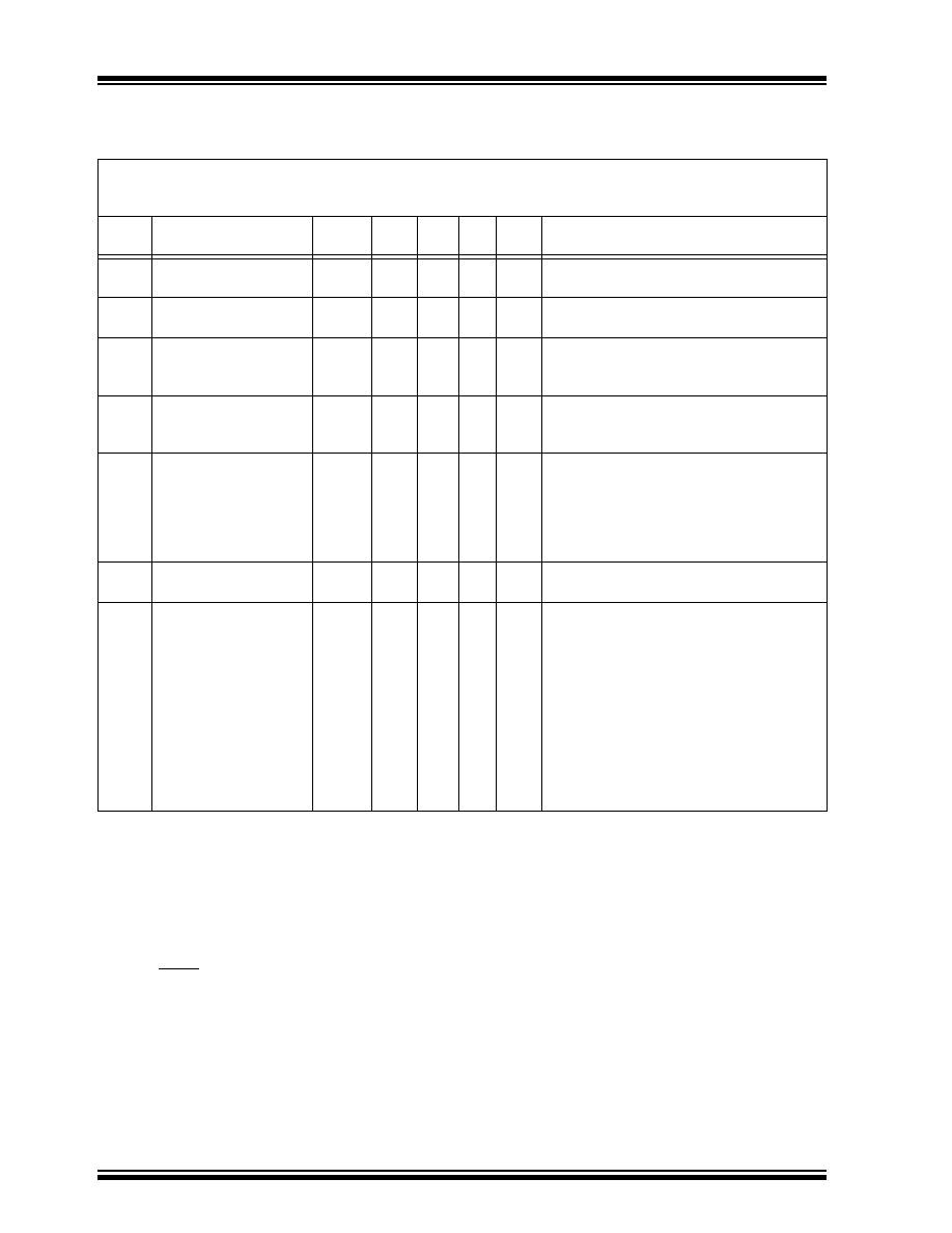
PIC16C9XX
DS30444E - page 142
©
1997 Microchip Technology Inc.
17.1
DC Characteristics:
PIC16C923/924-04 (Commercial, Industrial)
PIC16C923/924-08 (Commercial, Industrial)
DC CHARACTERISTICS
Standard Operating Conditions (unless otherwise stated)
Operating temperature
-40°C
T
A
+85°C for industrial and
0°C
T
A
+70°C for commercial
Param
No.
Characteristic
Sym
Min
Typ Max Units
Conditions
D001
D001A
Supply Voltage
V
DD
4.0
4.5
-
-
6.0
5.5
V
V
XT, RC and LP osc configuration
HS osc configuration
D002*
RAM Data Retention
Voltage (Note 1)
V
DR
-
1.5
-
V
D003
V
DD
start voltage to
ensure internal
Power-on Reset signal
V
POR
-
V
SS
-
V
See Power-on Reset section for details
D004*
V
DD
rise rate to ensure
internal Power-on
Reset signal
S
VDD
0.05
-
-
V/ms (Note 6) See Power-on Reset section for
details
D010
D011
D012
Supply Current (Note 2) I
DD
-
-
-
2.7
22.5
3.5
5
48
7
mA
µ
A
mA
XT and RC osc configuration
F
OSC
= 4 MHz, V
DD
= 5.5V (Note 4)
LP osc configuration,
F
OSC
= 32 kHz, V
DD
= 4.0V
HS osc configuration
F
OSC
= 8 MHz, V
DD
= 5.5V
D020
Power-down Current
(Note 3)
I
PD
-
1.5
21
µ
A
V
DD
= 4.0V
Module Differential Cur-
rent (Note 5)
D021
Watchdog Timer
I
WDT
-
6.0
20
µ
A
V
DD
= 4.0V
D022*
LCD Voltage Generation
w/internal RC osc
enabled
I
LCDRC
-
40
55
µ
A
V
DD
= 4.0V (Note 7)
D024*
LCD Voltage Generation
w/Timer1 @ 32.768 kHz
I
LCDT
1
-
33
60
µ
A
V
DD
= 4.0V (Note 7)
D025*
Timer1 oscillator
I
T
1
OSC
-
10.6
17
µ
A
V
DD
= 4.0V
D026*
A/D Converter
I
AD
-
1.0
-
µ
A
A/D on, not converting
*
These parameters are characterized but not tested.
Data in "Typ" column is at 5V, 25°C unless otherwise stated. These parameters are for design guidance only
and are not tested.
Note 1: This is the limit to which V
DD
can be lowered in SLEEP mode without losing RAM data.
2: The supply current is mainly a function of the operating voltage and frequency. Other factors such as I/O pin
loading and switching rate, oscillator type, internal code execution pattern, and temperature also have an
impact on the current consumption.
The test conditions for all I
DD
measurements in active operation mode are:
OSC1 = external square wave, from rail to rail; all I/O pins tristated, pulled to V
DD
MCLR = V
DD
.
3: The power-down current in SLEEP mode does not depend on the oscillator type. Power-down current is
measured with the part in SLEEP mode, with all I/O pins in hi-impedance state and tied to V
DD
and V
SS
.
4: For RC osc configuration, current through Rext is not included. The current through the resistor can be esti-
mated by the formula Ir = V
DD
/2Rext (mA) with Rext in kOhm.
5: The
current is the additional current consumed when this peripheral is enabled. This current should be
added to the base I
DD
or I
PD
measurement.
6: PWRT must be enabled for slow ramps.
7:
LCDT
1 and
LCDRC
includes the current consumed by the LCD Module and the voltage generation cir-
cuitry. This does not include current dissipated by the LCD panel.
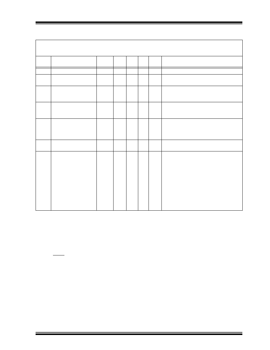
©
1997 Microchip Technology Inc.
DS30444E - page 143
PIC16C9XX
17.2
DC Characteristics:
PIC16LC923/924-04 (Commercial, Industrial)
DC CHARACTERISTICS
Standard Operating Conditions (unless otherwise stated)
Operating temperature
-40°C
T
A
+85°C for industrial and
0°C
T
A
+70°C for commercial
Param
No.
Characteristic
Sym
Min
Typ Max Units
Conditions
D001
Supply Voltage
V
DD
2.5
-
6.0
V
LP, XT, RC osc configuration
D002*
RAM Data Retention
Voltage (Note 1)
V
DR
-
1.5
-
V
D003
V
DD
start voltage to
ensure internal
Power-on Reset signal
V
POR
-
V
SS
-
V
See Power-on Reset section for details
D004*
V
DD
rise rate to ensure
internal Power-on
Reset signal
S
VDD
0.05
-
-
V/ms (Note 6) See Power-on Reset section for
details
D010
D011
Supply Current (Note 2) I
DD
-
-
2.0
13.5
3.8
30
mA
µ
A
XT and RC osc configuration
F
OSC
= 4 MHz, V
DD
= 3.0V (Note 4)
LP osc configuration,
F
OSC
= 32 kHz, V
DD
= 4.0V
D020
Power-down Current
(Note 3)
I
PD
-
0.9
5
µ
A
V
DD
= 3.0V
Module Differential Cur-
rent (Note 5)
D021
Watchdog Timer
I
WDT
-
6.0
20
µ
A
V
DD
= 3.0V
D022*
LCD Voltage Generation
w/internal RC osc
enabled
I
LCDRC
-
36
50
µ
A
V
DD
= 3.0V (Note 7)
D024*
LCD Voltage Generation
w/Timer1 @ 32.768 kHz
I
LCDT
1
-
15
29
µ
A
V
DD
= 3.0V (Note 7)
D025*
Timer1 oscillator
I
T
1
OSC
-
3.1
6.5
µ
A
V
DD
= 3.0V
D026*
A/D Converter
I
AD
-
1.0
-
µ
A
A/D on, not converting
*
These parameters are characterized but not tested.
Data in "Typ" column is at 5V, 25°C unless otherwise stated. These parameters are for design guidance only
and are not tested.
Note 1: This is the limit to which V
DD
can be lowered in SLEEP mode without losing RAM data.
2: The supply current is mainly a function of the operating voltage and frequency. Other factors such as I/O pin
loading and switching rate, oscillator type, internal code execution pattern, and temperature also have an
impact on the current consumption.
The test conditions for all I
DD
measurements in active operation mode are:
OSC1 = external square wave, from rail to rail; all I/O pins tristated, pulled to V
DD
MCLR = V
DD
.
3: The power-down current in SLEEP mode does not depend on the oscillator type. Power-down current is
measured with the part in SLEEP mode, with all I/O pins in hi-impedance state and tied to V
DD
and V
SS
.
4: For RC osc configuration, current through Rext is not included. The current through the resistor can be esti-
mated by the formula Ir = V
DD
/2Rext (mA) with Rext in kOhm.
5: The
current is the additional current consumed when this peripheral is enabled. This current should be
added to the base I
DD
or I
PD
measurement.
6: PWRT must be enabled for slow ramps.
7:
LCDT
1 and
LCDRC
includes the current consumed by the LCD Module and the voltage generation cir-
cuitry. This does not include current dissipated by the LCD panel.
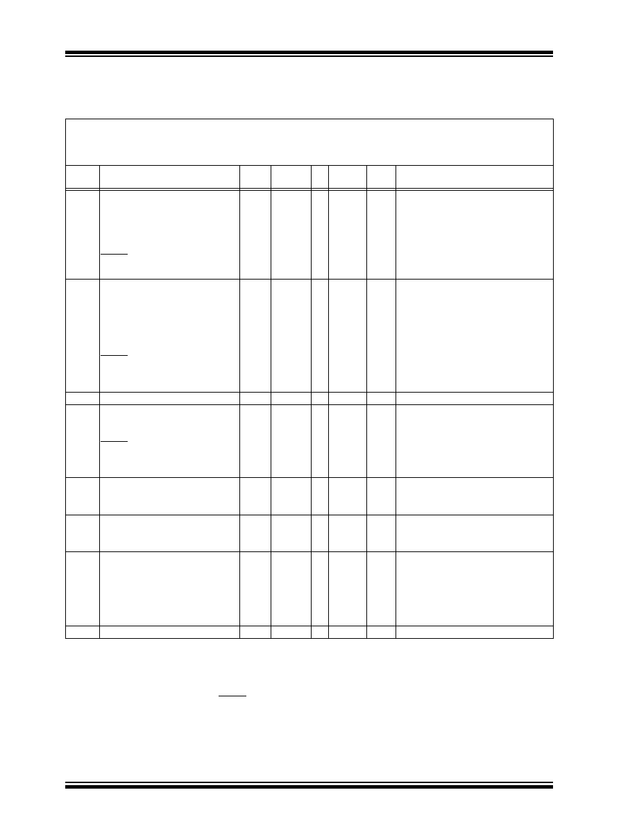
PIC16C9XX
DS30444E - page 144
©
1997 Microchip Technology Inc.
17.3
DC Characteristics:
PIC16C923/924-04 (Commercial, Industrial)
PIC16C923/924-08 (Commercial, Industrial)
PIC16LC923/924-04 (Commercial, Industrial)
DC CHARACTERISTICS
Standard Operating Conditions (unless otherwise stated)
Operating temperature
-40°C
T
A
+85°C for industrial and
0°C
T
A
+70°C for commercial
Operating voltage V
DD
range as described in DC spec
Param
No.
Characteristic
Sym
Min
Typ
Max
Units
Conditions
Input Low Voltage
I/O ports
V
IL
D030
with TTL buffer
V
SS
-
0.15V
DD
V
For entire V
DD
range
V
SS
-
0.8V
V
4.5V
V
DD
5.5V
D031
with Schmitt Trigger buffer
V
SS
-
0.2V
DD
V
D032
MCLR, OSC1 (in RC mode)
V
SS
-
0.2V
DD
V
D033
OSC1 (in XT, HS and LP)
V
SS
-
0.3V
DD
V
Note1
Input High Voltage
I/O ports
V
IH
-
D040
with TTL buffer
2.0
-
V
DD
V
4.5V
V
DD
5.5V
D040A
0.25V
DD
+ 0.8V
-
V
DD
V
For entire V
DD
range
D041
with Schmitt Trigger buffer
0.8V
DD
-
V
DD
V
D042
MCLR
0.8V
DD
-
V
DD
V
D042A OSC1 (XT, HS and LP)
0.7V
DD
-
V
DD
V
Note1
D043
OSC1 (in RC mode)
0.9V
DD
-
V
DD
V
D070
PORTB weak pull-up current
I
PURB
50
250
400
µ
A
V
DD
= 5V, V
PIN
= V
SS
Input Leakage Current
(Notes 2, 3)
D060
I/O ports
I
IL
-
-
±
1.0
µ
A
Vss
V
PIN
V
DD
, Pin at hi-Z
D061
MCLR, RA4/T0CKI
-
-
±
5
µ
A
Vss
V
PIN
V
DD
D063
OSC1
-
-
±
5
µ
A
Vss
V
PIN
V
DD
, XT, HS and LP osc
configuration
Output Low Voltage
D080
I/O ports
V
OL
-
-
0.6
V
I
OL
= 4.0 mA, V
DD
= 4.5V
D083
OSC2/CLKOUT (RC osc mode)
-
-
0.6
V
I
OL
= 1.6 mA, V
DD
= 4.5V
D090
Output High Voltage
I/O ports (Note 3)
V
OH
V
DD
- 0.7 -
-
V
I
OH
= -3.0 mA, V
DD
= 4.5V
D092
OSC2/CLKOUT (RC osc mode)
V
DD
- 0.7 -
-
V
I
OH
= -1.3 mA, V
DD
= 4.5V
Capacitive Loading Specs on
Output Pins
D100* OSC2 pin
C
OSC2
-
-
15
pF
In XT, HS and LP modes when exter-
nal clock is used to drive OSC1.
D101*
D102*
All I/O pins and OSC2 (in RC)
SCL, SDA in I
2
C mode
C
IO
C
B
-
-
-
-
50
400
pF
pF
D150* Open -Drain High Voltage
V
DD
-
-
14
V
RA4 pin
*
These parameters are characterized but not tested.
Data in "Typ" column is at 5V, 25
°
C unless otherwise stated. These parameters are for design guidance only
and are not tested.
Note 1: In RC oscillator configuration, the OSC1/CLKIN pin is a Schmitt Trigger input. It is not recommended that the
PIC16C9XX be driven with external clock in RC mode.
2: The leakage current on the MCLR pin is strongly dependent on the applied voltage level. The specified lev-
els represent normal operating conditions. Higher leakage current may be measured at different input volt-
ages.
3: Negative current is defined as current sourced by the pin.
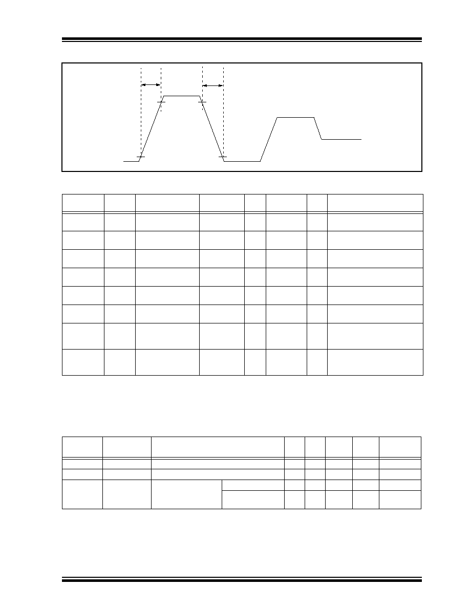
©
1997 Microchip Technology Inc.
DS30444E - page 145
PIC16C9XX
FIGURE 17-1: LCD VOLTAGE WAVEFORM
TABLE 17-2: LCD MODULE ELECTRICAL SPECIFICATIONS
TABLE 17-3: V
LCD
CHARGE PUMP ELECTRICAL SPECIFICATIONS
Parameter
No.
Sym
Characteristic
Min
Typ
Max
Units
Conditions
D200
V
LCD3
LCD Voltage on pin
V
LCD
3
V
DD
- 0.3
--
Vss + 7.0
V
D201
V
LCD2
LCD Voltage on pin
V
LCD
2
--
--
V
LCD
3
V
D202
V
LCD
1
LCD Voltage on pin
V
LCD
1
--
--
V
DD
V
D220*
V
OH
Output High
Voltage
Max V
LCDN
-
0.1
--
Max V
LCDN
V
COM outputs I
OH
= 25
µ
A
SEG outputs I
OH
= 3
µ
A
D221*
V
OL
Output Low Voltage
Min V
LCDN
--
Min V
LCDN
+
0.1
V
COM outputs I
OL
= 25
µ
A
SEG outputs I
OL
= 3
µ
A
D222*
F
LCDRC
L
CDRC
Oscillator Fre-
quency
5
15
50
kHz
V
DD
= 5V, -40°C to +85°C
D223*
Tr
LCD
Output Rise Time
--
--
200
µ
s
COM outputs Cload = 5,000 pF
SEG outputs Cload = 500 pF
V
DD
= 5.0V, T = 25
°
C
D224*
Tf
LCD
Output Fall Time (1)
--
--
200
µ
s
COM outputs Cload = 5,000 pF
SEG outputs Cload = 500 pF
V
DD
= 5.0V, T = 25
°
C
*
These parameters are characterized but not tested.
Data in "Typ" column is at 5V, 25
°
C unless otherwise stated. These parameters are for design guidance only and are not
tested.
(1) 0 ohm source impedance at V
LCD
.
Parameter
No.
Symbol
Characteristic
Min
Typ
Max
Units
Conditions
D250*
I
VADJ
VLCDADJ regulated current output
--
10
--
µ
A
D252*
I
VADJ
/
V
DD
VLCDADJ current V
DD
Rejection
--
--
0.1/1
µ
A/V
D265*
V
VADJ
VLCDADJ voltage limits
PIC16C92X
1.0
--
2.3
V
PIC16LC92X
1.0
V
DD
-
0.7V
V
V
DD
< 3V
*
These parameters are characterized but not tested.
Note
1: For design guidance only.
V
LCD
3
V
LCD
2
V
LCD
1
V
SS
D223
D224

PIC16C9XX
DS30444E - page 146
©
1997 Microchip Technology Inc.
17.4
Timing Parameter Symbology
The timing parameter symbols have been created following one of the following formats:
1. TppS2ppS
3. T
CC
:
ST
(I
2
C specifications only)
2. TppS
4. Ts
(I
2
C specifications only)
T
F
Frequency
T
Time
Lowercase letters (pp) and their meanings:
pp
cc
CCP1
osc
OSC1
ck
CLKOUT
rd
RD
cs
CS
rw
RD or WR
di
SDI
sc
SCK
do
SDO
ss
SS
dt
Data in
t0
T0CKI
io
I/O port
t1
T1CKI
mc
MCLR
wr
WR
Uppercase letters and their meanings:
S
F
Fall
P
Period
H
High
R
Rise
I
Invalid (Hi-impedance)
V
Valid
L
Low
Z
Hi-impedance
I
2
C only
AA
output access
High
High
BUF
Bus free
Low
Low
T
CC
:
ST
(I
2
C specifications only)
CC
HD
Hold
SU
Setup
ST
DAT
DATA input hold
STO
STOP condition
STA
START condition
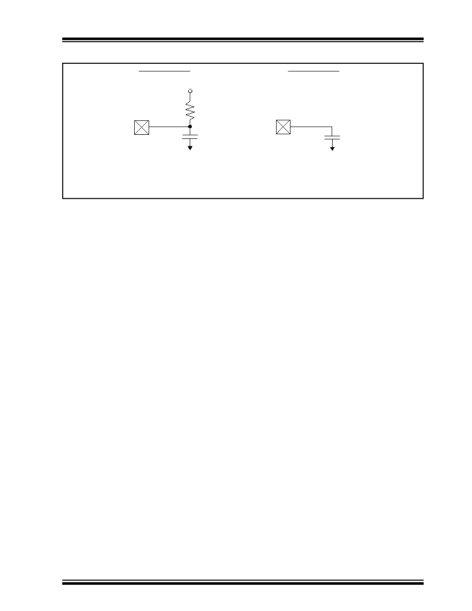
©
1997 Microchip Technology Inc.
DS30444E - page 147
PIC16C9XX
FIGURE 17-2: LOAD CONDITIONS
V
DD
/2
C
L
R
L
Pin
Pin
V
SS
V
SS
C
L
R
L
= 464
C
L
= 50 pF
for all pins except OSC2 unless otherwise noted.
15 pF
for OSC2 output
Load condition 1
Load condition 2
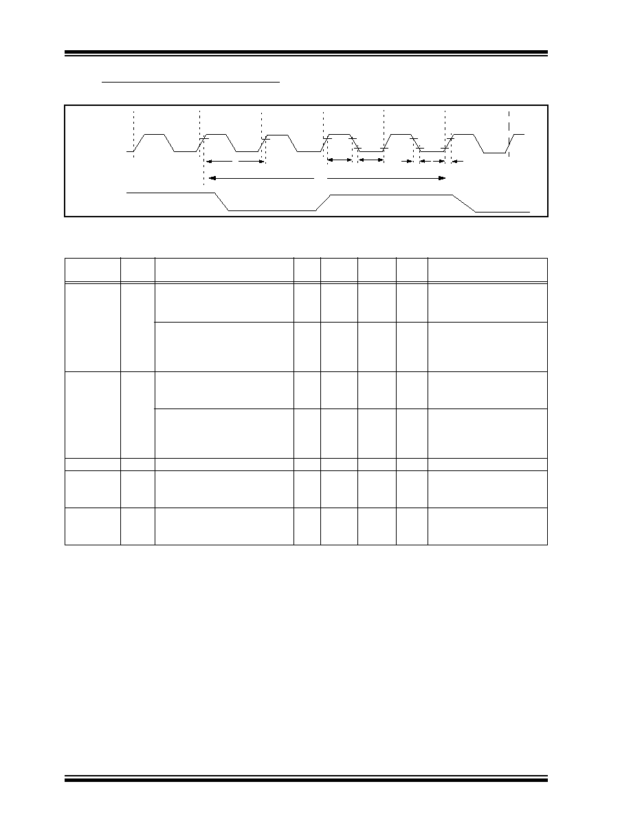
PIC16C9XX
DS30444E - page 148
©
1997 Microchip Technology Inc.
17.5
Timing Diagrams and Specifications
FIGURE 17-3: EXTERNAL CLOCK TIMING
TABLE 17-4: EXTERNAL CLOCK TIMING REQUIREMENTS
Parameter
No.
Sym
Characteristic
Min
Typ
Max
Units
Conditions
Fosc
External CLKIN Frequency
(Note 1)
DC
--
4
MHz
XT and RC osc mode
DC
--
8
MHz
HS osc mode
DC
--
200
kHz
LP osc mode
Oscillator Frequency
(Note 1)
DC
--
4
MHz
RC osc mode
0.1
--
4
MHz
XT osc mode
4
--
8
MHz
HS osc mode
5
--
200
kHz
LP osc mode
1
Tosc
External CLKIN Period
(Note 1)
250
--
--
ns
XT and RC osc mode
125
--
--
ns
HS osc mode
5
--
--
µ
s
LP osc mode
Oscillator Period
(Note 1)
250
--
--
ns
RC osc mode
250
--
10,000
ns
XT osc mode
125
--
250
ns
HS osc mode
5
--
--
µ
s
LP osc mode
2
T
CY
Instruction Cycle Time (Note 1)
500
--
DC
ns
T
CY
= 4/F
OSC
3
TosL,
TosH
External Clock in (OSC1) High or
Low Time
50
--
--
ns
XT oscillator
2.5
--
--
µ
s
LP oscillator
10
--
--
ns
HS oscillator
4
TosR,
TosF
External Clock in (OSC1) Rise or
Fall Time
--
--
25
ns
XT oscillator
--
--
50
ns
LP oscillator
--
--
15
ns
HS oscillator
Data in "Typ" column is at 5V, 25°C unless otherwise stated. These parameters are for design guidance only and are not
tested.
Note 1:
Instruction cycle period (T
CY
) equals four times the input oscillator time-base period. All specified values are based on
characterization data for that particular oscillator type under standard operating conditions with the device executing code.
Exceeding these specified limits may result in an unstable oscillator operation and/or higher than expected current con-
sumption. All devices are tested to operate at "min." values with an external clock applied to the OSC1/CLKIN pin.
When an external clock input is used, the "Max." cycle time limit is "DC" (no clock) for all devices.
OSC1
CLKOUT
Q4
Q1
Q2
Q3
Q4
Q1
1
2
3
3
4
4
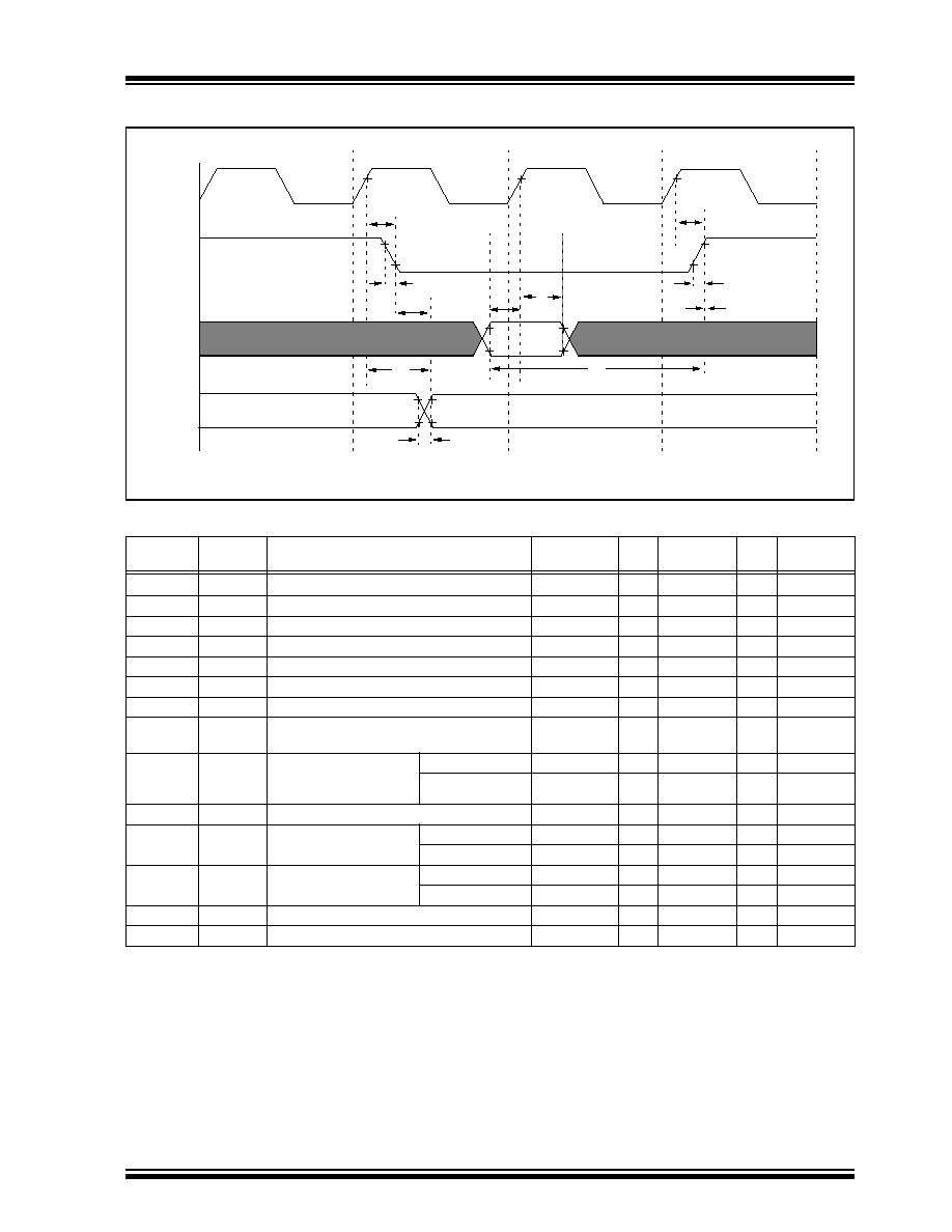
©
1997 Microchip Technology Inc.
DS30444E - page 149
PIC16C9XX
FIGURE 17-4: CLKOUT AND I/O TIMING
TABLE 17-5: CLKOUT AND I/O TIMING REQUIREMENTS
Parameter
No.
Sym
Characteristic
Min
Typ
Max
Units Conditions
10*
TosH2ckL
OSC1
to CLKOUT
--
75
200
ns
Note 1
11*
TosH2ckH
OSC1
to CLKOUT
--
75
200
ns
Note 1
12*
TckR
CLKOUT rise time
--
35
100
ns
Note 1
13*
TckF
CLKOUT fall time
--
35
100
ns
Note 1
14*
TckL2ioV
CLKOUT
to Port out valid
--
--
0.5T
CY
+ 20
ns
Note 1
15*
TioV2ckH
Port in valid before CLKOUT
Tosc + 200
--
--
ns
Note 1
16*
TckH2ioI
Port in hold after CLKOUT
0
--
--
ns
Note 1
17*
TosH2ioV
OSC1
(Q1 cycle) to
Port out valid
--
50
150
ns
18*
TosH2ioI
OSC1
(Q2 cycle) to
Port input invalid (I/O in
hold time)
PIC16C923/924
100
--
--
ns
PIC16LC923/924
200
--
--
ns
19*
TioV2osH
Port input valid to OSC1
(I/O in setup time)
0
--
--
ns
20*
TioR
Port output rise time
PIC16C923/924
--
10
40
ns
PIC16LC923/924
--
--
80
ns
21*
TioF
Port output fall time
PIC16C923/924
--
10
40
ns
PIC16LC923/924
--
--
80
ns
22*
Tinp
INT pin high or low time
T
CY
--
--
ns
23*
Trbp
RB7:RB4 change INT high or low time
T
CY
--
--
ns
*
These parameters are characterized but not tested.
Data in "Typ" column is at 5V, 25°C unless otherwise stated. These parameters are for design guidance
only and are not tested.
These parameters are asynchronous events not related to any internal clock edges.
Note 1:
Measurements are taken in RC Mode where CLKOUT output is 4 x T
OSC
.
Refer to Figure 17-2 for load conditions.
OSC1
CLKOUT
I/O Pin
(input)
I/O Pin
(output)
Q4
Q1
Q2
Q3
10
13
14
17
20, 21
19
18
15
11
12
16
old value
new value
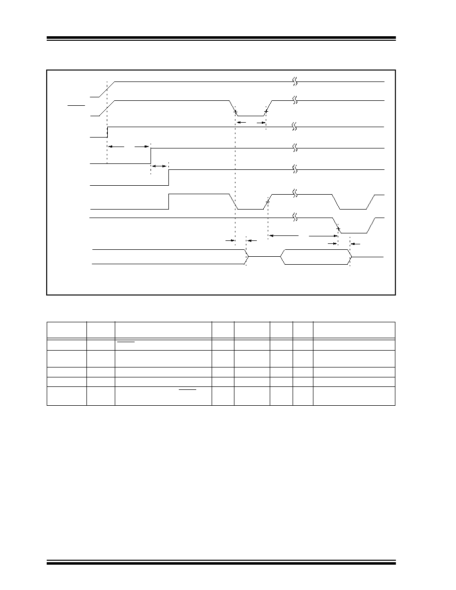
PIC16C9XX
DS30444E - page 150
©
1997 Microchip Technology Inc.
FIGURE 17-5: RESET, WATCHDOG TIMER, OSCILLATOR START-UP TIMER AND POWER-UP TIMER
TIMING
TABLE 17-6: RESET, WATCHDOG TIMER, OSCILLATOR START-UP TIMER AND POWER-UP TIMER
REQUIREMENTS
Parameter
No.
Sym
Characteristic
Min
Typ
Max
Units
Conditions
30
TmcL
MCLR Pulse Width (low)
2
--
--
µ
s
31*
Twdt
Watchdog Timer Time-out Period
(No Prescaler)
7
18
33
ms
V
DD
= 5V, -40°C to +85°C
32
Tost
Oscillation Start-up Timer Period
--
1024T
OSC
--
--
T
OSC
= OSC1 period
33*
Tpwrt
Power-up Timer Period
28
72
132
ms
V
DD
= 5V, -40°C to +85°C
34
T
IOZ
I/O Hi-impedance from MCLR Low
or Watchdog Timer Reset
--
--
2.1
µ
s
*
These parameters are characterized but not tested.
Data in "Typ" column is at 5V, 25°C unless otherwise stated. These parameters are for design guidance only and are not
tested.
V
DD
MCLR
Internal
POR
PWRT
Time-out
OSC
Time-out
Internal
RESET
Watchdog
Timer
RESET
33
32
30
31
34
I/O Pins
34
Refer to Figure 17-2 for load conditions.
©
1997 Microchip Technology Inc.
DS30444E - page 151
PIC16C9XX
FIGURE 17-6: TIMER0 AND TIMER1 EXTERNAL CLOCK TIMINGS
TABLE 17-7: TIMER0 AND TIMER1 EXTERNAL CLOCK REQUIREMENTS
Param
No.
Sym
Characteristic
Min
Typ
Max
Units Conditions
40*
Tt0H
T0CKI High Pulse Width
No Prescaler
0.5T
CY
+ 20
--
--
ns
Must also meet
parameter 42
With Prescaler
10
--
--
ns
41*
Tt0L
T0CKI Low Pulse Width
No Prescaler
0.5T
CY
+ 20
--
--
ns
Must also meet
parameter 42
With Prescaler
10
--
--
ns
42*
Tt0P
T0CKI Period
No Prescaler
T
CY
+ 40
--
--
ns
With Prescaler
Greater of:
20 or T
CY
+ 40
N
--
--
ns
N = prescale value
(2, 4, ..., 256)
45*
Tt1H
T1CKI High Time
Synchronous, Prescaler = 1
0.5T
CY
+ 20
--
--
ns
Must also meet
parameter 47
Synchronous,
Prescaler =
2,4,8
PIC16C923/924
15
--
--
ns
PIC16LC923/924
25
--
--
ns
Asynchronous
PIC16C923/924
30
--
--
ns
PIC16LC923/924
50
--
--
ns
46*
Tt1L
T1CKI Low Time
Synchronous, Prescaler = 1
0.5T
CY
+ 20
--
--
ns
Must also meet
parameter 47
Synchronous,
Prescaler =
2,4,8
PIC16C923/924
15
--
--
ns
PIC16LC923/924
25
--
--
ns
Asynchronous
PIC16C923/924
30
--
--
ns
PIC16LC923/924
50
--
--
ns
47*
Tt1P
T1CKI input period Synchronous
PIC16C923/924
Greater of:
30
OR
T
CY
+ 40
N
--
--
ns
N = prescale value
(1, 2, 4, 8)
PIC16LC923/924
Greater of:
50
OR
T
CY
+ 40
N
N = prescale value
(1, 2, 4, 8)
Asynchronous
PIC16C923/924
60
--
--
ns
PIC16LC923/924
100
--
--
ns
Ft1
Timer1 oscillator input frequency range
(oscillator enabled by setting bit T1OSCEN)
DC
--
200
kHz
48
TCKEZtmr1 Delay from external clock edge to timer increment
2Tosc
--
7Tosc
--
*
These parameters are characterized but not tested.
Data in "Typ" column is at 5V, 25°C unless otherwise stated. These parameters are for design guidance only and are not
tested.
46
47
45
48
41
42
40
RA4/T0CKI
RC0/T1OSO/T1CKI
TMR0 or
TMR1
Refer to Figure 17-2 for load conditions.
PIC16C9XX
DS30444E - page 152
©
1997 Microchip Technology Inc.
FIGURE 17-7: CAPTURE/COMPARE/PWM TIMINGS
TABLE 17-8: CAPTURE/COMPARE/PWM REQUIREMENTS
Parameter
No.
Sym Characteristic
Min
Typ Max Units Conditions
50*
TccL Input Low Time
No Prescaler
0.5T
CY
+ 20
--
--
ns
With Prescaler PIC16C923/924
10
--
--
ns
PIC16LC923/924
20
--
--
ns
51*
TccH Input High Time
No Prescaler
0.5T
CY
+ 20
--
--
ns
With Prescaler PIC16C923/924
10
--
--
ns
PIC16LC923/924
20
--
--
ns
52*
TccP Input Period
3T
CY
+ 40
N
--
--
ns
N = prescale value
(1,4 or 16)
53*
TccR Output Rise Time
PIC16C923/924
--
10
25
ns
PIC16LC923/924
--
25
45
ns
54*
TccF Output Fall Time
PIC16C923/924
--
10
25
ns
PIC16LC923/924
--
25
45
ns
*
These parameters are characterized but not tested.
Data in "Typ" column is at 5V, 25°C unless otherwise stated. These parameters are for design guidance only and are not
tested.
RC2/CCP1
(Capture Mode)
50
51
52
53
54
RC2/CCP1
(Compare or PWM Mode)
Refer to Figure 17-2 for load conditions.
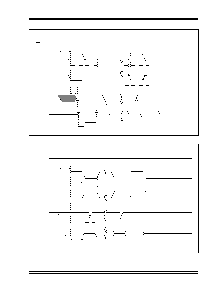
©
1997 Microchip Technology Inc.
DS30444E - page 153
PIC16C9XX
FIGURE 17-8: SPI MASTER MODE TIMING (CKE = 0)
FIGURE 17-9: SPI MASTER MODE TIMING (CKE = 1)
SS
SCK
(CKP = 0)
SCK
(CKP = 1)
SDO
SDI
70
71
72
73
74
75, 76
78
79
80
79
78
MSb
LSb
BIT6 - - - - - -1
MSb IN
LSb IN
BIT6 - - - -1
Refer to Figure 17-2 for load conditions.
SS
SCK
(CKP = 0)
SCK
(CKP = 1)
SDO
SDI
81
71
72
74
75, 76
78
80
MSb
79
73
MSb IN
BIT6 - - - - - -1
LSb IN
BIT6 - - - -1
LSb
Refer to Figure 17-2 for load conditions.
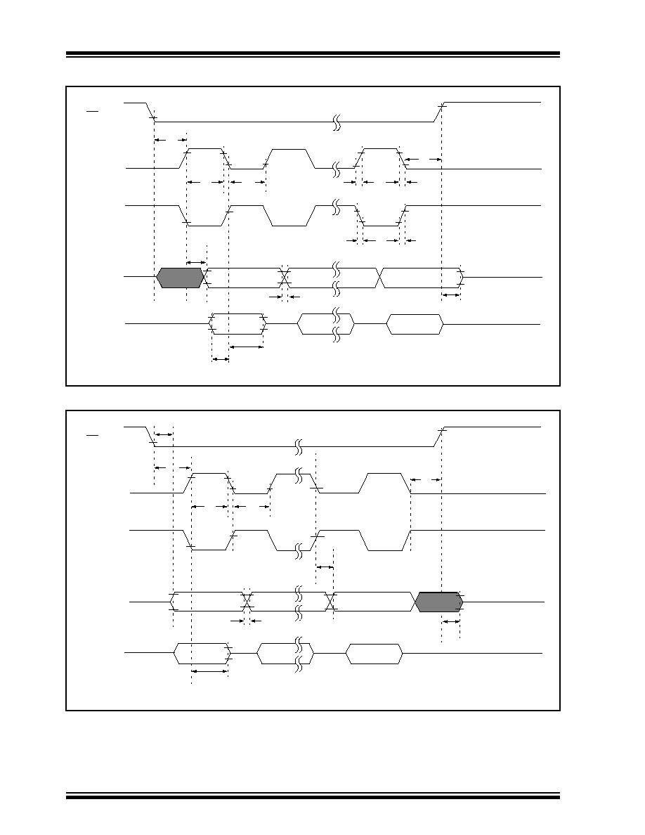
PIC16C9XX
DS30444E - page 154
©
1997 Microchip Technology Inc.
FIGURE 17-10:SPI SLAVE MODE TIMING (CKE = 0)
FIGURE 17-11:SPI SLAVE MODE TIMING (CKE = 1)
SS
SCK
(CKP = 0)
SCK
(CKP = 1)
SDO
SDI
70
71
72
73
74
75, 76
77
78
79
80
79
78
SDI
MSb
LSb
BIT6 - - - - - -1
MSb IN
BIT6 - - - -1
LSb IN
83
Refer to Figure 17-2 for load conditions.
SS
SCK
(CKP = 0)
SCK
(CKP = 1)
SDO
SDI
70
71
72
82
SDI
74
75, 76
MSb
BIT6 - - - - - -1
LSb
77
MSb IN
BIT6 - - - -1
LSb IN
80
83
Refer to Figure 17-2 for load conditions.
©
1997 Microchip Technology Inc.
DS30444E - page 155
PIC16C9XX
TABLE 17-9: SPI MODE REQUIREMENTS
Param
No.
Sym
Characteristic
Min
Typ
Max
Units
Conditions
70*
TssL2scH,
TssL2scL
SS
to SCK
or SCK
input
T
CY
--
--
ns
71*
71A*
TscH
SCK input high time (slave
mode)
Continuous
1.25T
CY
+
30
--
--
ns
Single Byte
40
--
--
ns
72*
72A*
TscL
SCK input low time (slave
mode)
Continuous
1.25T
CY
+
30
--
--
ns
Single Byte
40
73*
TdiV2scH,
TdiV2scL
Setup time of SDI data input to SCK edge
50
--
--
ns
74*
TscH2diL,
TscL2diL
Hold time of SDI data input to SCK edge
50
--
--
ns
75*
TdoR
SDO data output rise time
--
10
25
ns
76*
TdoF
SDO data output fall time
--
10
25
ns
77*
TssH2doZ
SS
to SDO output hi-impedance
10
--
50
ns
78*
TscR
SCK output rise time (master mode)
--
10
25
ns
79*
TscF
SCK output fall time (master mode)
--
10
25
ns
80*
TscH2doV,
TscL2doV
SDO data output valid after SCK edge
--
--
50
ns
81*
TdoV2scH,
TdoV2scL
SDO data output setup to SCK edge
T
CY
--
--
ns
82*
TssL2doV
SDO data output valid after SS
edge
--
--
50
ns
83*
TscH2ssH,
TscL2ssH
SS
after SCK edge
1.5T
CY
+ 40
--
--
ns
84*
Tb2b
Delay between consecutive bytes
1.5T
CY
+ 40
--
--
ns
*
Characterized but not tested.
Data in "Typ" column is at 5V, 25°C unless otherwise stated. These parameters are for design guidance only and are not
tested.
PIC16C9XX
DS30444E - page 156
©
1997 Microchip Technology Inc.
FIGURE 17-12:I
2
C BUS START/STOP BITS TIMING
TABLE 17-10:I
2
C BUS START/STOP BITS REQUIREMENTS
Parameter
No.
Sym
Characteristic
Min
Typ
Max
Units
Conditions
90*
T
SU
:
STA
START condition
Setup time
100 kHz mode
4700
--
--
ns
Only relevant for repeated START
condition
91*
T
HD
:
STA
START condition
Hold time
100 kHz mode
4000
--
--
ns
After this period the first clock
pulse is generated
92*
T
SU
:
STO
STOP condition
Setup time
100 kHz mode
4700
--
--
ns
93*
T
HD
:
STO
STOP condition
Hold time
100 kHz mode
4000
--
--
ns
*
Characterized but not tested.
91
93
SCL
SDA
START
Condition
STOP
Condition
90
92
Refer to Figure 17-2 for load conditions.
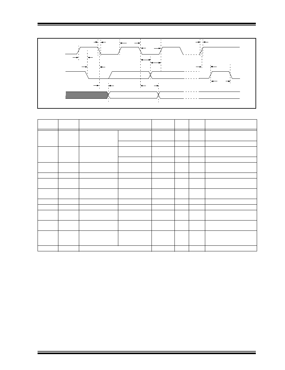
©
1997 Microchip Technology Inc.
DS30444E - page 157
PIC16C9XX
FIGURE 17-13:I
2
C BUS DATA TIMING
TABLE 17-11:I
2
C BUS DATA REQUIREMENTS
Parameter
No.
Sym
Characteristic
Min
Max
Units
Conditions
100*
T
HIGH
Clock high time
100 kHz mode
4.0
--
µ
s
Device must operate at a mini-
mum of 1.5 MHz
SSP Module
1.5T
CY
--
101*
T
LOW
Clock low time
100 kHz mode
4.7
--
µ
s
Device must operate at a mini-
mum of 1.5 MHz
SSP Module
1.5T
CY
--
102*
T
R
SDA and SCL rise
time
100 kHz mode
--
1000
ns
103*
T
F
SDA and SCL fall time
100 kHz mode
--
300
ns
90*
T
SU
:
STA
START condition
setup time
100 kHz mode
4.7
--
µ
s
Only relevant for repeated
START condition
91*
T
HD
:
STA
START condition hold
time
100 kHz mode
4.0
--
µ
s
After this period the first clock
pulse is generated
106*
T
HD
:
DAT
Data input hold time
100 kHz mode
0
--
ns
107*
T
SU
:
DAT
Data input setup time
100 kHz mode
250
--
ns
92*
T
SU
:
STO
STOP condition setup
time
100 kHz mode
4.7
--
µ
s
109*
T
AA
Output valid from
clock
100 kHz mode
--
3500
ns
Note 1
110*
T
BUF
Bus free time
100 kHz mode
4.7
--
µ
s
Time the bus must be free
before a new transmission can
start
D102*
Cb
Bus capacitive loading
--
400
pF
*
Characterized but not tested.
Note 1:
As a transmitter, the device must provide this internal minimum delay time to bridge the undefined region (min. 300 ns) of
the falling edge of SCL to avoid unintended generation of START or STOP conditions.
90
91
92
100
101
103
106
107
109
109
110
102
SCL
SDA
In
SDA
Out
Refer to Figure 17-2 for load conditions.
PIC16C9XX
DS30444E - page 158
©
1997 Microchip Technology Inc.
TABLE 17-12:A/D CONVERTER CHARACTERISTICS:
PIC16C924-04 (COMMERCIAL, INDUSTRIAL)
PIC16LC924-04 (COMMERCIAL, INDUSTRIAL)
Param
No.
Sym Characteristic
Min
Typ
Max
Units
Conditions
A01
N
R
Resolution
--
--
8-bits
bit
V
REF
= V
DD
= 5.12V,
V
SS
V
AIN
V
REF
A02
E
ABS
Total Absolute error
--
--
<
±
1
LSb
V
REF
= V
DD
= 5.12V,
V
SS
V
AIN
V
REF
A03
E
IL
Integral linearity error
--
--
<
±
1
LSb
V
REF
= V
DD
= 5.12V,
V
SS
V
AIN
V
REF
A04
E
DL
Differential linearity error
--
--
<
±
1
LSb
V
REF
= V
DD
= 5.12V,
V
SS
V
AIN
V
REF
A05
E
FS
Full scale error
--
--
<
±
1
LSb
V
REF
= V
DD
= 5.12V,
V
SS
V
AIN
V
REF
A06
E
OFF
Offset error
--
--
<
±
1
LSb
V
REF
= V
DD
= 5.12V,
V
SS
V
AIN
V
REF
A10
--
Monotonicity
--
guaranteed
--
--
V
SS
V
AIN
V
REF
A20
V
REF
Reference voltage
3.0V
--
V
DD
+ 0.3
V
A25
V
AIN
Analog input voltage
V
SS
- 0.3
--
V
REF
+ 0.3
V
A30
Z
AIN
Recommended impedance of
analog voltage source
--
--
10.0
k
A40
I
AD
A/D conversion current
(V
DD
)
PIC16C924
--
180
--
µ
A
Average current consump-
tion when A/D is on.
(Note 1)
PIC16LC924
--
90
--
µ
A
A50
I
REF
V
REF
input current (Note 2)
10
--
--
--
1000
10
µ
A
µ
A
During V
AIN
acquisition.
Based on differential of
V
HOLD
to V
AIN
to charge
C
HOLD
, see Section 12.1.
During A/D Conversion
cycle
*
These parameters are characterized but not tested.
Data in "Typ" column is at 5V, 25
°
C unless otherwise stated. These parameters are for design guidance only and are not
tested.
Note 1:
When A/D is off, it will not consume any current other than minor leakage current.
The power-down current spec includes any such leakage from the A/D module.
2:
V
REF
current is from RA3 pin or V
DD
pin, whichever is selected as reference input.
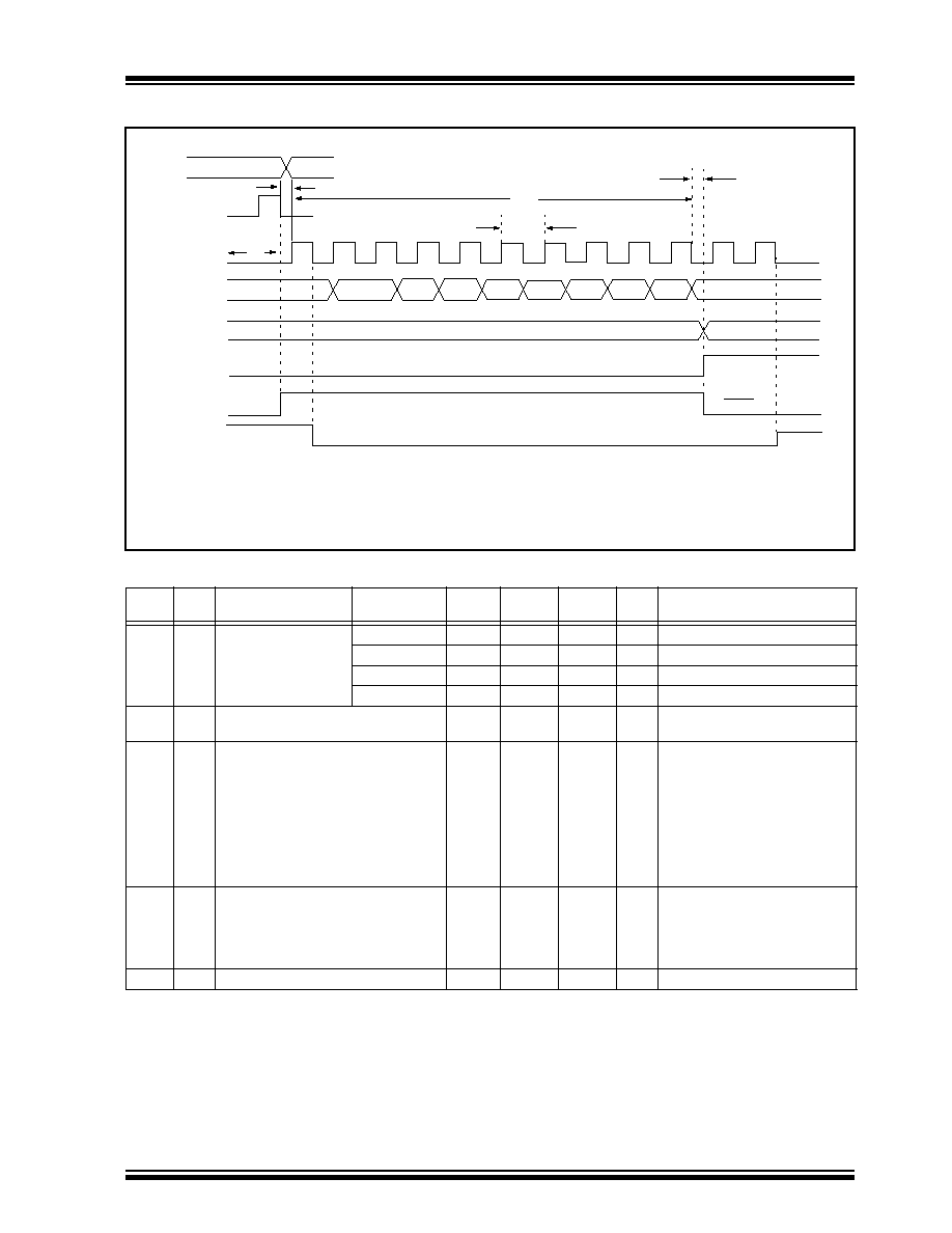
©
1997 Microchip Technology Inc.
DS30444E - page 159
PIC16C9XX
FIGURE 17-14:A/D CONVERSION TIMING
TABLE 17-13:A/D CONVERSION REQUIREMENTS
Param
No.
Sym
Characteristic
Min
Typ
Max
Units
Conditions
130
T
AD
A/D clock period
PIC16C924
1.6
--
--
µ
s
T
OSC
based, V
REF
3.0V
PIC16LC924
2.0
--
--
µ
s
T
OSC
based, V
REF
full range
PIC16C924
2.0
4.0
6.0
µ
s
A/D RC Mode
PIC16LC924
3.0
6.0
9.0
µ
s
A/D RC Mode
131
T
CNV
Conversion time (not including S/H time)
(Note 1)
--
9.5
--
T
AD
132
T
ACQ
Acquisition time
Note 2
5*
20
--
--
--
µ
s
µ
s
The minimum time is the amplifier
settling time. This may be used if
the "new" input voltage has not
changed by more than 1 LSb (i.e.,
20.0 mV @ 5.12V) from the last
sampled voltage (as stated on
C
HOLD
).
134
T
GO
Q4 to A/D clock start
--
T
OSC
/2 §
--
--
If the A/D clock source is selected
as RC, a time of T
CY
is added
before the A/D clock starts. This
allows the
SLEEP
instruction to be
executed.
135
T
SWC
Switching from convert
sample time
1.5 §
--
--
T
AD
*
These parameters are characterized but not tested.
Data in "Typ" column is at 5V, 25
°
C unless otherwise stated. These parameters are for design guidance only and are not
tested.
§
This specification ensured by design.
Note 1:
ADRES register may be read on the following T
CY
cycle.
2:
See Section 12.1 for min conditions.
131
130
132
BSF ADCON0, GO
Q4
A/D CLK
A/D DATA
ADRES
ADIF
GO
SAMPLE
OLD_DATA
SAMPLING STOPPED
DONE
NEW_DATA
(T
OSC
/2)
(1)
7
6
5
4
3
2
1
0
Note 1:
If the A/D clock source is selected as RC, a time of T
CY
is added before the A/D clock starts. This allows the
SLEEP
instruction to be executed.
1 T
CY
134

PIC16C9XX
DS30444E - page 160
©
1997 Microchip Technology Inc.
NOTES:
©
1997 Microchip Technology Inc.
DS30444E - page 161
PIC16C9XX
18.0
DC AND AC CHARACTERISTICS GRAPHS AND TABLES
The graphs and tables provided in this section are for design guidance and are not tested or guaranteed.
In some graphs or tables the data presented are outside specified operating range (i.e., outside specified V
DD
range). This is for information only and devices are guaranteed to operate properly only within the specified
range.
Note:
The data presented in this section is a statistical summary of data collected on units from different lots over
a period of time and process characterization samples. 'Typical' represents the mean of the distribution at,
25
°
C, while 'max' or 'min' represents (mean +3
) and (mean -3
) respectively where
is standard devia-
tion.
FIGURE 18-1: TYPICAL I
PD
vs. V
DD
(WDT
DISABLED, RC MODE @
25
°
C)
FIGURE 18-2: MAXIMUM I
PD
vs. V
DD
(WDT
DISABLED, RC MODE -40
°
C
TO +85
°
C)
180
160
140
120
100
2.5
3.0
3.5
4.0
4.5
5.0
5.5
I
PD
(nA)
V
DD
(V
OLTS
)
6.0
200
220
240
260
280
1.0
0.5
0.0
2.5
3.0
3.5
4.0
4.5
5.0
5.5
I
PD
(
µ
A)
V
DD
(V
OLTS
)
6.0
1.5
2.0
2.5
3.0
3.5
FIGURE 18-3: TYPICAL I
PD
vs. V
DD
(WDT
ENABLED, RC MODE @
25
°
C)
FIGURE 18-4: MAXIMUM I
PD
vs. V
DD
(WDT
ENABLED, RC MODE -40
°
C TO
+85
°
C)
5.0
0.0
2.5
3.0
3.5
4.0
4.5
5.0
5.5
I
PD
(
µ
A)
V
DD
(V
OLTS
)
6.0
10.0
15.0
20.0
25.0
25.0
20.0
15.0
10.0
5.0
2.5
3.0
3.5
4.0
4.5
5.0
5.5
I
PD
(
µ
A)
V
DD
(V
OLTS
)
6.0
30.0
35.0
40.0
0.0
PIC16C9XX
DS30444E - page 162
©
1997 Microchip Technology Inc.
FIGURE 18-5: TYPICAL I
PD
vs. V
DD
(LCD
ON
(1)
, INTERNAL RC
(2)
, RC
MODE @ 25
°
C)
FIGURE 18-6: MAXIMUM I
PD
vs. V
DD
(LCD ON
(32 kHz
(1)
), INTERNAL RC (32
kHz
(2)
), RC MODE -40
°
C TO
+85
°
C)
50
45
40
35
30
2.5
3.0
3.5
4.0
4.5
5.0
5.5
I
PD
(
µ
A)
V
DD
(V
OLTS
)
6.0
55
60
C Spec @ 4.0V = 41
LC Spec @ 3.0V = 37
50
45
40
35
30
2.5
3.0
3.5
4.0
4.5
5.0
5.5
I
PD
(
µ
A)
V
DD
(V
OLTS
)
6.0
55
60
C Spec @ 4.0V = 45
LC Spec @ 3.0V = 40
65
70
FIGURE 18-7: TYPICAL I
PD
vs. V
DD
(LCD
ON
(1)
, TIMER1 (32 kHz
(2)
), RC
MODE @ 25
°
C)
FIGURE 18-8: MAXIMUM I
PD
vs. V
DD
(LCD
ON
(1)
, TIMER1(32 kHz
(2)
), RC
MODE -40
°
C TO +85
°
C)
40
30
20
10
0
2.5
3.0
3.5
4.0
4.5
5.0
5.5
I
PD
(
µ
A)
V
DD
(V
OLTS
)
6.0
50
60
70
80
90
80
60
40
20
0
2.5
3.0
3.5
4.0
4.5
5.0
5.5
I
PD
(
µ
A)
V
DD
(V
OLTS
)
6.0
100
120
140
160
180
Note 1: The LCD module is turned on, internal charge pump enabled, 1/4 MUX, 32 Hz frame frequency and no load
on LCD segments/commons. I
PD
will increase depending on the LCD panel connected to the PIC16C9XX.
Note 2: Indicates the clock source to the LCD module.
Data based on
process char
acter
ization s
amples
.
See fi
rst page of this section f
or details
.
©
1997 Microchip Technology Inc.
DS30444E - page 163
PIC16C9XX
FIGURE 18-9: TYPICAL RC OSCILLATOR
FREQUENCY vs. V
DD
FIGURE 18-10:TYPICAL RC OSCILLATOR
FREQUENCY vs. V
DD
FIGURE 18-11:TYPICAL RC OSCILLATOR
FREQUENCY vs. V
DD
2.5
3.0
3.5
4.0
4.5
5.0
5.5
6.0
V
DD
(V
OLTS
)
6.0
5.5
5.0
4.5
4.0
3.5
3.0
2.5
2.0
1.5
1.0
0.5
0.0
Fosc(MHz)
Cext = 22 pF, T = 25
°
C
R = 100k
R = 10k
R = 5k
Shaded area is beyond recommended range.
2.5
3.0
3.5
4.0
4.5
5.0
5.5
6.0
V
DD
(V
OLTS
)
2.4
2.2
2.0
1.8
1.6
1.4
1.2
1.0
0.8
0.6
0.4
0.2
0.0
Fosc(MHz)
Cext = 100 pF, T = 25
°
C
R = 100k
R = 10k
R = 5k
R = 3.3k
2.5
3.0
3.5
4.0
4.5
5.0
5.5
6.0
V
DD
(V
OLTS
)
1000
900
800
700
600
500
400
300
200
100
0
Fosc(kHz)
Cext = 300 pF, T = 25
°
C
R = 3.3k
R = 5k
R = 10k
R = 100k
FIGURE 18-12:TYPICAL I
PD
vs. TIMER1
ENABLED (32 kHz, RC0/RC1 =
33 pF/33 pF, RC MODE)
FIGURE 18-13:MAXIMUM I
PD
vs. TIMER1
ENABLED
(32 kHz, RC0/RC1 = 33 pF/33
pF, 85
°
C TO -40
°
C, RC MODE)
30
25
20
15
10
5
0
2.5
3.0
3.5
4.0
4.5
5.0
5.5
6.0
V
DD
(V
OLTS
)
I
PD
(
µ
A)
30
25
20
15
10
5
0
2.5
3.0
3.5
4.0
4.5
5.0
5.5
6.0
V
DD
(Volts)
I
PD
(
µ
A)
35
40
45
Data based on
process char
acter
ization s
amples
.
See fi
rst page of this section f
or details
.
PIC16C9XX
DS30444E - page 164
©
1997 Microchip Technology Inc.
FIGURE 18-14:TYPICAL I
DD
vs. FREQUENCY (RC MODE @ 20 pF, 25
°
C)
FIGURE 18-15:MAXIMUM I
DD
vs. FREQUENCY (RC MODE @ 20 pF, -40
°
C TO +85
°
C)
2000
2500
1500
1000
500
0
0.0
1.00
2.00
3.00
4.00
Frequency (MHz)
I
DD
(
µ
A)
Shaded area is
6.0V
5.5V
5.0V
4.5V
4.0V
3.5V
3.0V
2.5V
beyond recommended range
5.00
Typical 2.7 mA @ 4 MHz, 5.5V
2000
3500
1500
1000
500
0
0.0
1.00
2.00
3.00
4.00
Frequency (MHz)
I
DD
(
µ
A)
Shaded area is
6.0V
5.5V
5.0V
4.5V
4.0V
3.5V
3.0V
2.5V
beyond recommended range
5.00
Maximum 5.0 mA @ 4 MHz, 5.5V
2500
3000
Data based on
process char
acter
ization s
amples
.
See fi
rst page of this section f
or details
.
©
1997 Microchip Technology Inc.
DS30444E - page 165
PIC16C9XX
FIGURE 18-16:TYPICAL I
DD
vs. FREQUENCY (RC MODE @ 100 pF, 25
°
C)
FIGURE 18-17:MAXIMUM I
DD
vs. FREQUENCY (RC MODE @ 100 pF, -40
°
C TO +85
°
C)
1400
1200
1000
800
600
400
200
0
0
200
400
600
800
1000
1200
1400
1600
Frequency (kHz)
I
DD
(
µ
A)
6.0V
5.5V
5.0V
4.5V
4.0V
3.5V
3.0V
2.5V
Shaded area is
beyond recommended range
1600
1400
1200
1000
800
600
400
200
0
0
200
400
600
800
1000
1200
1400
1600
Frequency (kHz)
I
DD
(
µ
A)
6.0V
5.5V
5.0V
4.5V
4.0V
3.5V
3.0V
2.5V
Shaded area is
beyond recommended range
Data based on
process char
acter
ization s
amples
.
See fi
rst page of this section f
or details
.
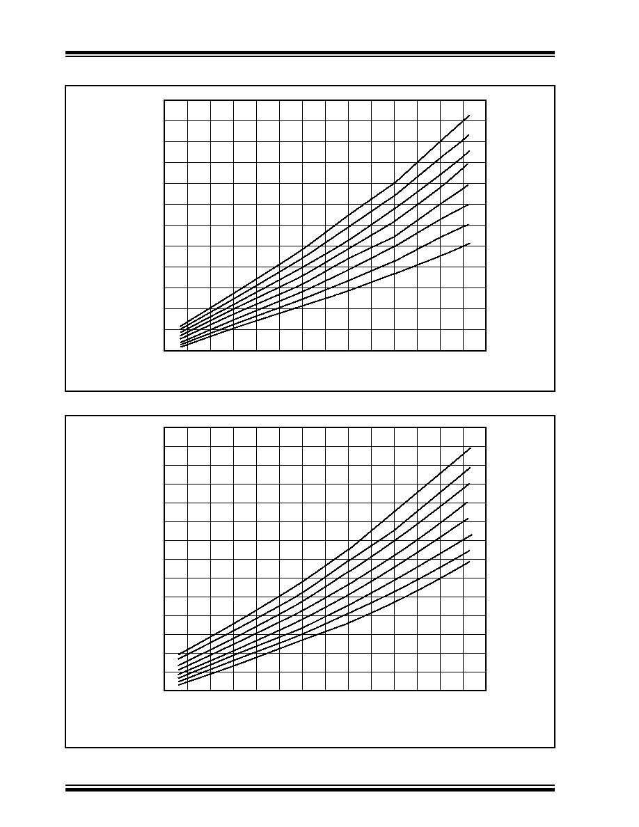
PIC16C9XX
DS30444E - page 166
©
1997 Microchip Technology Inc.
FIGURE 18-18:TYPICAL I
DD
vs. FREQUENCY (RC MODE @ 300 pF, 25
°
C)
FIGURE 18-19:MAXIMUM I
DD
vs. FREQUENCY (RC MODE @ 300 pF, -40
°
C TO +85
°
C)
1200
1000
800
600
400
200
0
0
100
200
300
400
500
600
700
Frequency (kHz)
I
DD
(
µ
A)
6.0V
5.5V
5.0V
4.5V
4.0V
3.5V
3.0V
2.5V
1200
1000
800
600
400
200
0
0
100
200
300
400
500
600
700
Frequency (kHz)
I
DD
(
µ
A)
6.0V
5.5V
5.0V
4.5V
4.0V
3.5V
3.0V
2.5V
1400
Data based on
process char
acter
ization s
amples
.
See fi
rst page of this section f
or details
.
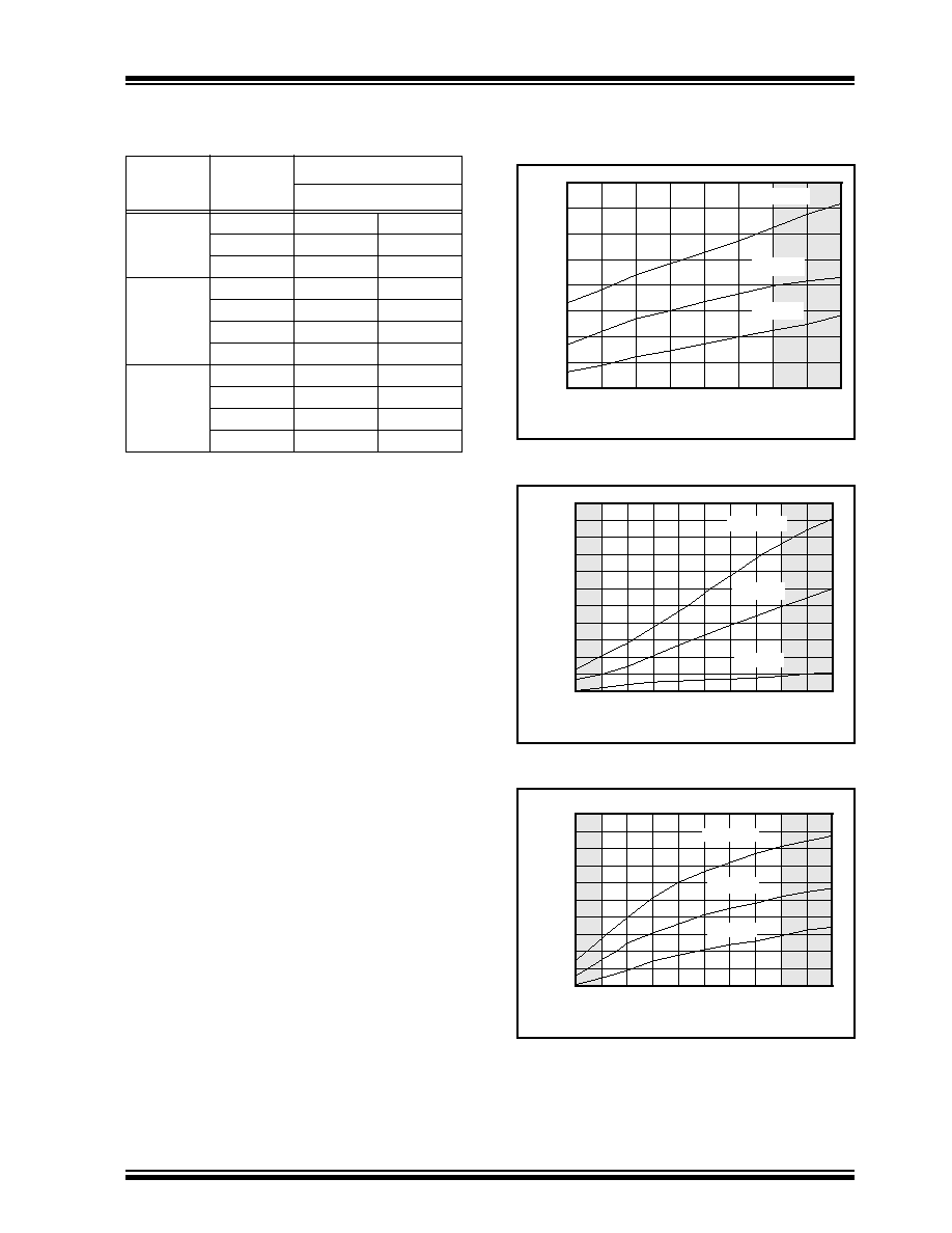
©
1997 Microchip Technology Inc.
DS30444E - page 167
PIC16C9XX
TABLE 18-1: RC OSCILLATOR
FREQUENCIES
Cext
Rext
Average
Fosc @ 5V, 25
°
C
22 pF
5k
4.12 MHz
±
1.4%
10k
2.35 MHz
±
1.4%
100k
268 kHz
±
1.1%
100 pF
3.3k
1.80 MHz
±
1.0%
5k
1.27 MHz
±
1.0%
10k
688 kHz
±
1.2%
100k
77.2 kHz
±
1.0%
300 pF
3.3k
707 kHz
±
1.4%
5k
501 kHz
±
1.2%
10k
269 kHz
±
1.6%
100k
28.3 kHz
±
1.1%
The percentage variation indicated here is part to
part variation due to normal process distribution. The
variation indicated is
±
3 standard deviation from
average value for V
DD
= 5V.
FIGURE 18-20:TRANSCONDUCTANCE(gm)
OF HS OSCILLATOR vs. V
DD
FIGURE 18-21:TRANSCONDUCTANCE(gm)
OF LP OSCILLATOR vs. V
DD
FIGURE 18-22:TRANSCONDUCTANCE(gm)
OF XT OSCILLATOR vs. V
DD
4.0
3.0
3.5
4.0
4.5
5.0
5.5
6.0
6.5
7.0
gm(
m
A/V)
V
DD
(V
OLTS
)
3.5
3.0
2.5
2.0
1.5
1.0
0.5
0.0
Max -40
°
C
Typ 25
°
C
Min 85
°
C
Shaded area is
beyond recommended range
110
100
90
80
70
60
50
40
30
20
10
0
2.0
2.5
3.0
3.5
4.0
4.5
5.0
5.5
6.0
6.5
7.0
gm(
µ
A/V)
V
DD
(V
OLTS
)
Max -40
°
C
Typ 25
°
C
Min 85
°
C
Shaded areas are
beyond recommended range
1000
900
800
700
600
500
400
300
200
100
0
2.0
2.5
3.0
3.5
4.0
4.5
5.0
5.5
6.0
6.5
7.0
gm(
µ
A/V)
V
DD
(V
OLTS
)
Max -40
°
C
Typ 25
°
C
Min 85
°
C
Shaded areas are
beyond recommended range
Data based on
process char
acter
ization s
amples
.
See fi
rst page of this section f
or details
.
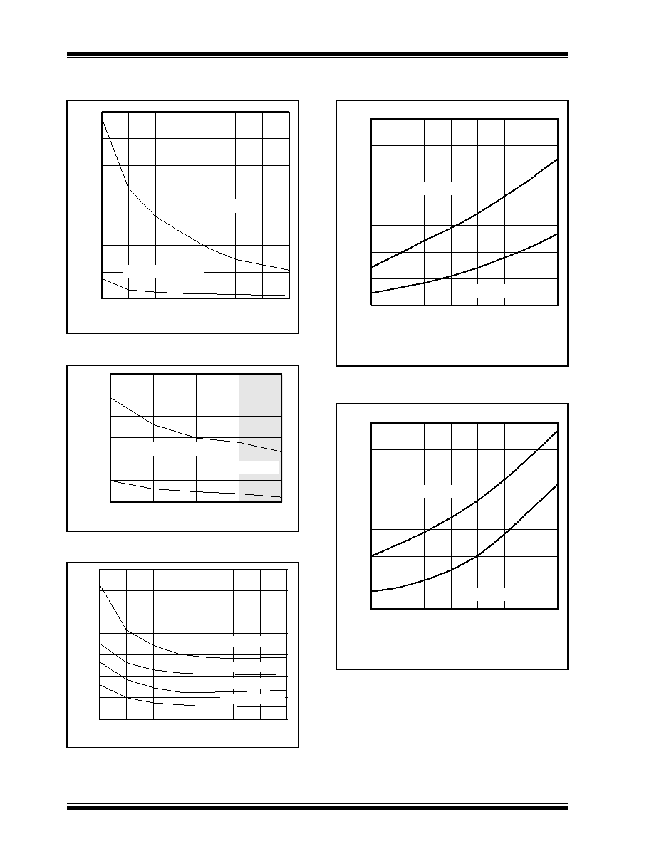
PIC16C9XX
DS30444E - page 168
©
1997 Microchip Technology Inc.
FIGURE 18-23:TYPICAL XTAL STARTUP TIME
vs. V
DD
(LP MODE, 25
°
C)
FIGURE 18-24:TYPICAL XTAL STARTUP TIME
vs. V
DD
(HS MODE, 25
°
C)
FIGURE 18-25:TYPICAL XTAL STARTUP TIME
vs. V
DD
(XT MODE, 25
°
C)
3.5
3.0
2.5
2.0
1.5
1.0
0.5
0.0
2.5
3.0
3.5
4.0
4.5
5.0
5.5
6.0
V
DD
(V
OLTS
)
Star
tup
Time(Seconds)
32 kHz, 33 pF/33 pF
200 kHz, 15 pF/15 pF
7
6
5
4
3
2
1
4.0
4.5
5.0
5.5
6.0
V
DD
(V
OLTS
)
Star
tup
Time(ms)
8 MHz, 33 pF/33 pF
8 MHz, 15 pF/15 pF
70
60
50
40
30
20
10
0
3.0
3.5
2.5
4.0
5.0
5.5
6.0
4.5
V
DD
(V
OLTS
)
Star
tup
Time(ms)
200 kHz, 68 pF/68 pF
200 kHz, 47 pF/47 pF
1 MHz, 15 pF/15 pF
4 MHz, 15 pF/15 pF
FIGURE 18-26:TYPICAL I
DD
vs. V
DD
(LP MODE @ 25
°
C)
FIGURE 18-27:MAXIMUM I
DD
vs. V
DD
(LP MODE -40
°
C TO +85
°
C)
140
120
100
80
60
40
20
0
2.5
3.0
3.5
4.0
4.5
5.0
5.5
6.0
V
DD
(V
OLTS
)
I
DD
(
µ
A)
32 kHz, 33 pF/33 pF
200 kHz, 15 pF/15 pF
LC Spec -> Typical = 22.5
µ
A, 32 kHz, 4.0V
2.5
3.0
3.5
4.0
4.5
5.0
5.5
6.0
V
DD
(V
OLTS
)
I
DD
(
µ
A)
32 kHz, 33 pF/33 pF
200 kHz, 15 pF/15 pF
LC Spec -> Maximum = 48
µ
A, 32 kHz, 4.0V
140
120
100
80
60
40
20
0
Data based on
process char
acter
ization s
amples
.
See fi
rst page of this section f
or details
.
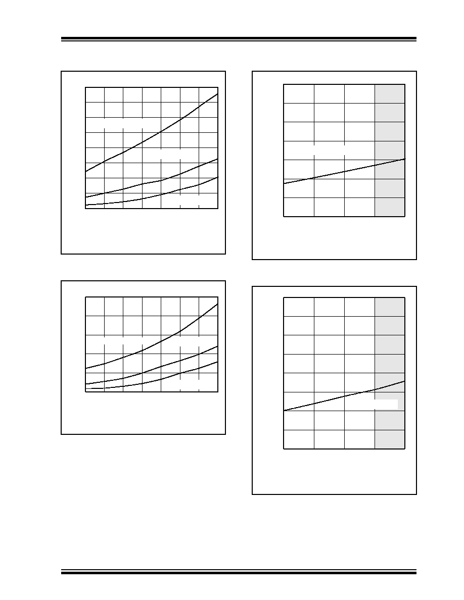
©
1997 Microchip Technology Inc.
DS30444E - page 169
PIC16C9XX
FIGURE 18-28:TYPICAL I
DD
vs. V
DD
(XT MODE @ 25
°
C)
FIGURE 18-29:MAXIMUM I
DD
vs. V
DD
(XT MODE -40
°
C TO +85
°
C)
1400
1200
1000
800
600
400
200
0
2.5
3.0
3.5
4.0
4.5
5.0
5.5
6.0
V
DD
(V
OLTS
)
I
DD
(
µ
A)
200 kHz, 33 pF/33 pF
4 MHz, 15 pF/15 pF
Typical = 2.7
µ
A, 4 MHz, 5.5V
1600
1 MHz, 15 pF/15 pF
2000
1500
1000
500
0
2.5
3.0
3.5
4.0
4.5
5.0
5.5
6.0
V
DD
(V
OLTS
)
I
DD
(
µ
A)
200 kHz, 33 pF/33 pF
4 MHz, 15 pF/15 pF
Maximum = 5 mA, 4 MHz, 5.5V
2500
1 MHz, 15 pF/15 pF
FIGURE 18-30:TYPICAL I
DD
vs. V
DD
(HS MODE @ 25
°
C)
FIGURE 18-31:MAXIMUM I
DD
vs. V
DD
(HS MODE -40
°
C TO +85
°
C)
7
6
5
4
3
2
1
0
4.0
4.5
5.0
5.5
6.0
V
DD
(V
OLTS
)
I
DD
(
µ
A)
Typical = 3.5 mA, 8 MHz, 5.5V
8 MHz, 15 pF/15 pF
7
6
5
4
3
2
1
0
4.0
4.5
5.0
5.5
6.0
V
DD
(V
OLTS
)
I
DD
(
M
A)
Maximum = 7 mA, 8 MHz, 5.5V
8 MHz, 15 pF/15 pF
8
Data based on
process char
acter
ization s
amples
.
See fi
rst page of this section f
or details
.

PIC16C9XX
DS30444E - page 170
©
1997 Microchip Technology Inc.
NOTES:
©
1997 Microchip Technology Inc.
DS30444E - page 171
PIC16C9XX
19.0
PACKAGING INFORMATION
19.1
64-Lead Plastic Surface Mount (TQFP 10x10x1 mm Body 1.0/0.10 mm Lead Form))
Package Group: Plastic TQFP
Symbol
Millimeters
Inches
Min
Nominal
Max
Min
Nominal
Max
0
°
-
7
°
0
°
-
7
°
A
-
-
1.20
-
-
0.047
A1
0.05
0.10
0.15
0.002
0.004
0.006
A2
0.95
1.00
1.05
0.037
0.039
0.041
b
0.17
0.22
0.27
0.007
0.009
0.011
b1
0.17
0.20
0.23
0.007
0.008
0.009
D
-
12.00
-
-
0.472
-
D1
-
10.00
-
-
0.394
-
E
-
12.00
-
-
0.472
-
E1
-
10.00
-
-
0.394
-
e
-
0.50
-
-
0.020
-
L
0.45
0.60
0.75
0.018
0.024
0.030
N
64
64
64
64
64
64
D
D/2
E
E/2
e
8 Places
11/13
°
A
See Detail B
0.09/0.20
b1
b
0.09/0.16
Base Metal
with Lead Finish
A2
A1
0.08
R min.
0.20 min.
1.00 ref.
L
0-7
°
Datum Plane
Gauge Plane
0.25
0
°
min.
DETAIL B
A
e/2
A
See Detail A
DETAIL A
E1
D1
PIC16C9XX
DS30444E - page 172
©
1997 Microchip Technology Inc.
19.2
64-Lead Plastic Dual In-line (750 mil)
Package Group: Plastic Dual In-Line (PLA)
Symbol
Millimeters
Inches
Min
Max
Notes
Min
Max
Notes
0
°
15
°
0
°
15
°
A
5.08
0.200
A1
0.51
0.020
A2
3.38
4.27
0.133
0.168
B
0.38
0.56
0.015
0.022
B1
.076
1.27
Typical
0.030
0.050
Typical
C
0.20
0.30
Typical
0.008
0.012
Typical
D
57.40
57.91
2.260
2.280
D1
55.12
55.12
Reference
2.170
2.170
Reference
E
19.05
19.69
0.750
0.775
E1
16.76
17.27
0.660
0.680
e1
1.73
1.83
Typical
0.068
0.072
Typical
eA
19.05
19.05
Reference
0.750
0.750
Reference
eB
19.05
21.08
0.750
0.830
L
3.05
3.43
0.120
0.135
N
64
64
64
64
S
1.19
0.047
S1
0.686
0.027
N
Pin No. 1
E1
E
S
D
B1
B
Base
Plane
Seating
Plane
S1
A1 A2 A
L
e1
C
e
A
D1
e
B
Indicator Area
©
1997 Microchip Technology Inc.
DS30444E - page 173
PIC16C9XX
19.3
68-Lead Plastic Leaded Chip Carrier (Square)
Package Group: Plastic Leaded Chip Carrier (PLCC)
Symbol
Millimeters
Inches
Min
Max
Notes
Min
Max
Notes
A
4.191
4.699
0.165
0.185
A1
2.286
2.794
0.090
0.110
D
25.019
25.273
0.985
0.995
D1
24.130
24.334
0.950
0.958
D2
22.860
23.622
0.900
0.930
D3
20.320
-
Reference
0.800
-
Reference
E
25.019
25.273
0.985
0.995
E1
24.130
24.334
0.950
0.958
E2
22.860
23.622
0.900
0.930
E3
20.320
-
Reference
0.800
-
Reference
N
68
-
68
-
CP
-
0.102
-
0.004
LT
0.203
0.254
0.008
0.010
S
0.177
.007
B D-E
-A-
0.254
D
1
D
3
3
3
-C-
-F-
-D-
4
9
8
-B-
-E-
S
0.177
.007
A F-G
S
S
E
E
1
-H-
-G-
6
2
3
.010 Max
1.524
.060
10
2
11
0.508
.020
1.651
.065
R 1.14/0.64
.045/.025
R 1.14/0.64
.045/.025
1.651
.065
0.508
.020
-H-
11
0.254
.010 Max
6
Min
0.812/0.661
.032/.026
3
-C-
0.64
.025
Min
5
0.533/0.331
.021/.013
0.177
.007 M A
F-G S , D-E S
1.27
.050
2 Sides
A
S
0.177
.007
B A
S
D
3
/E
3
D
2
0.101
.004
0.812/0.661
.032/.026
S
0.38
.015
F-G
4
S
0.38
.015
F-G
E
2
D
-H-
A
1
Seating
Plane
2 Sides
N Pics
PIC16C9XX
DS30444E - page 174
©
1997 Microchip Technology Inc.
19.4
Package Marking Information
Legend:
MM...M
XX...X
AA
BB
C
D1
E
Microchip part number information
Customer specific information*
Year code (last 2 digits of calender year)
Week code (week of January 1 is week '01')
Facility code of the plant at which wafer is manufactured.
C = Chandler, Arizona, U.S.A.
Mask revision number for microcontroller
Assembly code of the plant or country of origin in which
part was assembled.
In the event the full Microchip part number cannot be marked on one
line, it will be carried over to the next line thus limiting the number of
available characters for customer specific information.
Note:
Standard OTP marking consists of Microchip part number, year code, week code,
facility code, mask revision number, and assembly code. For OTP marking beyond
this, certain price adders apply. Please check with your Microchip Sales Office.
For QTP devices, any special marking adders are included in QTP price.
*
68-Lead PLCC
MMMMMMMMMM
MMMMMMM
AABBCDE
Example
S = Tempe, Arizona, U.S.A.
64-Lead TQFP
MMMMMMM
AABBCDE
MMMMMMMMMM
Example
9712CAE
68-Lead CERQUAD Windowed
Example
AABBCDE
64-Lead SDIP (Shrink DIP)
MMMMMMMMMMMMMMMMM
Example
PIC16C924
-08/L
9648CAE
MMMMMMMMMMMMMMMMM
AABBCDE
PIC16C924-04/CL
9650CAE
-08I/PT
PIC16C923
9736CAE
PIC16C924-04I/SP

©
1997 Microchip Technology Inc.
DS30444E - page 175
PIC16C9XX
APPENDIX A:
The following are the list of modifications over the
PIC16C5X microcontroller family:
1.
Instruction word length is increased to 14-bits.
This allows larger page sizes both in program
memory (4K now as opposed to 512 before) and
register file (192 bytes now versus 32 bytes
before).
2.
A PC high latch register (PCLATH) is added to
handle program memory paging. Bits PA2, PA1,
PA0 are removed from STATUS register.
3.
Data memory paging is redefined slightly. STA-
TUS register is modified.
4.
Four new instructions have been added:
RETURN, RETFIE, ADDLW
, and
SUBLW
.
Two instructions TRIS and OPTION are being
phased out although they are kept for compati-
bility with PIC16C5X.
5.
OPTION and TRIS registers are made address-
able.
6.
Interrupt capability is added. Interrupt vector is
at 0004h.
7.
Stack size is increased to 8 deep.
8.
Reset vector is changed to 0000h.
9.
Reset of all registers is revisited. Five different
reset (and wake-up) types are recognized. Reg-
isters are reset differently.
10. Wake up from SLEEP through interrupt is
added.
11. Two separate timers, Oscillator Start-up Timer
(OST) and Power-up Timer (PWRT) are
included for more reliable power-up. These tim-
ers are invoked selectively to avoid unnecessary
delays on power-up and wake-up.
12. PORTB has weak pull-ups and interrupt on
change feature.
13. T0CKI pin is also a port pin (RA4) now.
14. FSR is made a full eight bit register.
15. "In-circuit programming" is made possible. The
user can program PIC16CXX devices using only
five pins: V
DD
, V
SS
, MCLR/V
PP
, RB6 (clock) and
RB7 (data in/out).
16. PCON status register is added with a Power-on
Reset status bit (POR).
17. Code protection scheme is enhanced such that
portions of the program memory can be pro-
tected, while the remainder is unprotected.
APPENDIX B: COMPATIBILITY
To convert code written for PIC16C5X to PIC16CXX,
the user should take the following steps:
1.
Remove any program memory page select oper-
ations (PA2, PA1, PA0 bits) for
CALL
,
GOTO
.
2.
Revisit any computed jump operations (write to
PC or add to PC, etc.) to make sure page bits are
set properly under the new scheme.
3.
Eliminate any data memory page switching.
Redefine data variables to reallocate them.
4.
Verify all writes to STATUS, OPTION, and FSR
registers since these have changed.
5.
Change reset vector to 0000h.

PIC16C9XX
DS30444E - page 176
©
1997 Microchip Technology Inc.
APPENDIX C: WHAT'S NEW
Figure 13-13 (Resistor Ladder and Charge Pump) in
LCD Section.
Parameter D150 - Open Drain High Voltage.
DC and AC Characterization Graphs and Tables.
APPENDIX D: WHAT'S CHANGED
Various descriptions for clarity.
Example code for Changing prescaler assignment
between Timer0 and the WDT.
The A/D section has many changes that provide
greater clarification of A/D operation.
The Instruction Set has Q-cycle activity listings for
every instruction.
The following Electrical Characteristic Parameter val-
ues have changed to:
D011 (Standard Voltage Devices, C)
Typical
22.5
µ
A
Max
48
µ
A
D022 (Standard Voltage Devices)
Typical
40
µ
A
Max
55
µ
A
D024 (Standard Voltage Devices)
Typical
33
µ
A
Max
60
µ
A
D001 (Extended Voltage Devices, LC)
Min
2.5
V
D011 (Extended Voltage Devices, LC)
Typical
13.5
µ
A
Max
30
µ
A
D022 (Extended Voltage Devices, LC)
Typical
36
µ
A
Max
50
µ
A
D024 (Extended Voltage Devices, LC)
Typical
15
µ
A
Max
29
µ
A
D030 (with TTL)
Max
0.5V
DD
V (
ENTIRE
RANGE
)
Max
0.8V
V (4.5V
V
DD
5.5V)
D201, D202
Deleted D210 and D211, D251, D253, D260, D271
D222
Min
5
kHz
Typical
15
kHz
Max
50
kHz
D223, D224 - units to ns.
Added D265 (VLCDADJ voltage limits.
Changed parameters:
12 - TckR
35 ns Typical
13 - TckF
35 ns Typical
15 - TioV2ckH
Tosc + 200 ns Min
18 - TosH2ioL
200 ns Min (LC devices)
30 - TmcL
2
µ
s Min
34 - Tioz
2.1
µ
s Max
Timer0 and Timer1 External Clock Timings - Various.
53 - TccR,
54 - TccF
73 - TdiV2scH
50 ns Min
74 - TscH2diL
50 ns Min
Combined A/D specification tables for Standard and
Extended Voltage devices.

©
1997 Microchip Technology Inc.
DS30444E - page 177
PIC16C9XX
INDEX
A
A/D
Accuracy/Error ............................................................ 86
ADCON0 ............................................................... 79, 80
ADCON1 ............................................................... 79, 80
ADIF............................................................................ 80
Analog-to-Digital Converter......................................... 79
Configuring Analog Port.............................................. 83
Connection Considerations......................................... 87
Conversion time .......................................................... 85
Conversions ................................................................ 84
Converter Characteristics ......................................... 158
Faster Conversion - Lower Resolution Tradeoff ......... 85
GO/DONE ................................................................... 80
Internal Sampling Switch (Rss) Impedance ................ 82
Operation During Sleep .............................................. 86
Sampling Requirements.............................................. 82
Sampling Time ............................................................ 82
Source Impedance...................................................... 82
Transfer Function........................................................ 87
A/D Conversion Clock ......................................................... 83
Registers
Section ........................................................................ 19
Absolute Maximum Ratings .............................................. 141
ACK............................................................. 70, 74, 75, 76, 77
ADCON0 Register............................................................... 19
ADCON1 Register............................................................... 20
ADIE bit ............................................................................... 26
ADIF bit ............................................................................... 27
ADRES............................................................ 19, 79, 80, 109
ALU ....................................................................................... 9
Application Notes
AN546 ......................................................................... 79
AN552 ......................................................................... 33
AN556 ......................................................................... 29
AN578 ......................................................................... 63
AN594 ......................................................................... 57
AN607 ....................................................................... 107
Architecture
Harvard ......................................................................... 9
Overview ....................................................................... 9
von Neumann................................................................ 9
Assembler
MPASM Assembler................................................... 138
B
BF ....................................................................................... 74
Block Diagrams
A/D .............................................................................. 81
Capture Mode ............................................................. 58
Compare Mode ........................................................... 58
External Brown-out1 ................................................. 112
External Brown-out2 ................................................. 112
External Parallel Cystal Oscillator............................. 105
External Power-on Reset .......................................... 112
External Series Crystal Oscillator ............................. 105
Interrupt Logic ........................................................... 114
LCD Module ................................................................ 90
On-Chip Reset Circuit ............................................... 106
PIC16C923 ................................................................. 10
PIC16C924 ................................................................. 11
PORTC ....................................................................... 35
PORTD ................................................................. 36, 37
PORTE........................................................................ 38
PORTF ........................................................................39
PORTG........................................................................40
PWM............................................................................59
RA3:RA0 and RA5 Port Pins .......................................31
RA4/T0CKI Pin ............................................................31
RB3:RB0 Port Pins ......................................................33
RB7:RB4 Port Pins ......................................................33
RC Oscillator ............................................................ 105
SSP (I
2
C Mode)...........................................................73
SSP (SPI Mode) ..........................................................65
Timer0 .........................................................................45
Timer0/WDT Prescaler ................................................48
Timer1 .........................................................................52
Timer2 .........................................................................55
Watchdog Timer ....................................................... 116
Brown-out Protection Circuit ............................................. 112
C
C bit .....................................................................................23
Capture/Compare/PWM (CCP)
Capture Mode..............................................................58
CCP1 ...........................................................................57
CCP1CON ................................................................ 109
CCPR1H................................................................... 109
CCPR1L ................................................................... 109
Compare Mode............................................................58
Compare Mode Block Diagram ...................................58
Prescaler .....................................................................58
PWM Block Diagram ...................................................59
PWM Mode..................................................................59
PWM, Example Frequencies/Resolutions ...................60
Section.........................................................................57
Carry bit .................................................................................9
CCP1CON Register.............................................................19
CCP1IE bit ...........................................................................26
CCP1IF bit ...........................................................................27
CCPR1H Register ...............................................................19
CCPR1L Register ................................................................19
Clocking Scheme.................................................................15
Code Examples
Call of a Subroutine in Page 1 from Page 0 ................30
Changing Between Capture Prescalers ......................58
Changing Prescaler (Timer0 to WDT) .........................49
Changing Prescaler (WDT to Timer0) .........................49
Doing an A/D Conversion ............................................84
I/O Programming .........................................................41
I
2
C Module Operation..................................................78
Indirect Addressing......................................................30
Initializing PORTA .......................................................31
Initializing PORTB .......................................................33
Initializing PORTC .......................................................35
Initializing PORTD .......................................................36
Initializing PORTE .......................................................38
Initializing PORTF........................................................39
Initializing PORTG .......................................................40
Loading the SSPBUF register .....................................65
Reading a 16-bit Free-running Timer ..........................53
Code Protection ........................................................ 103, 118
Computed GOTO ................................................................29
Configuration Bits ............................................................. 103
D
DC bit...................................................................................23
DC Characteristics.................................................... 142, 143
Development Support ....................................................... 137
Development Tools........................................................... 137
Digit Carry bit .........................................................................9

PIC16C9XX
DS30444E - page 178
©
1997 Microchip Technology Inc.
Direct Addressing................................................................ 30
E
Electrical Characteristics................................................... 141
External Power-on Reset Circuit ....................................... 112
F
Family of Devices
PIC16C9XX................................................................... 6
FSR ................................................................................... 108
FSR Register............................................... 19, 20, 21, 22, 30
Fuzzy Logic Dev. System (
fuzzyTECH
®
-MP)................... 139
G
GIE .................................................................................... 113
I
I/O Ports
Section ........................................................................ 31
I/O Programming Considerations........................................ 41
I
2
C
Addressing I
2
C Devices .............................................. 70
Arbitration.................................................................... 72
BF ......................................................................... 74, 75
CKP............................................................................. 76
Clock Synchronization ................................................ 72
Combined Format ....................................................... 71
I
2
C Overview ............................................................... 69
Initiating and Terminating Data Transfer..................... 69
Master-Receiver Sequence ........................................ 71
Master-Transmitter Sequence .................................... 71
Multi-master ................................................................ 72
START ........................................................................ 69
STOP .................................................................... 69, 70
Transfer Acknowledge ................................................ 70
ICEPIC Low-Cost PIC16CXXX In-Circuit Emulator .......... 137
IDLE_MODE ....................................................................... 78
In-Circuit Serial Programming ................................... 103, 118
INDF.................................................................................. 108
INDF Register ............................................. 19, 20, 21, 22, 30
Indirect Addressing ............................................................. 30
Instruction Cycle.................................................................. 15
Instruction Flow/Pipelining .................................................. 15
Instruction Format ............................................................. 119
Instruction Set
ADDLW ..................................................................... 121
ADDWF ..................................................................... 121
ANDLW ..................................................................... 122
ANDWF ..................................................................... 122
BCF ........................................................................... 122
BSF ........................................................................... 123
BTFSC ...................................................................... 123
BTFSS ...................................................................... 124
CALL ......................................................................... 124
CLRF......................................................................... 125
CLRW ....................................................................... 125
CLRWDT................................................................... 126
COMF ....................................................................... 126
DECF ........................................................................ 126
DECFSZ.................................................................... 127
GOTO ....................................................................... 127
INCF.......................................................................... 128
INCFSZ ..................................................................... 128
IORLW ...................................................................... 129
IORWF ...................................................................... 129
MOVF........................................................................ 130
MOVLW .................................................................... 130
MOVWF .................................................................... 130
NOP .......................................................................... 131
OPTION .................................................................... 131
RETFIE ..................................................................... 131
RETLW ..................................................................... 132
RETURN................................................................... 132
RLF ........................................................................... 133
RRF .......................................................................... 133
SLEEP ...................................................................... 134
SUBLW ..................................................................... 134
SUBWF..................................................................... 135
SWAPF ..................................................................... 135
TRIS ......................................................................... 135
XORLW .................................................................... 136
XORWF .................................................................... 136
Section...................................................................... 119
INT Interrupt...................................................................... 115
INTCON ............................................................ 109, 113, 115
INTCON Register................................ 19, 20, 21, 22, 25, 102
INTEDG ............................................................................ 115
INTEDG bit ......................................................................... 24
Inter-Integrated Circuit (I
2
C) ............................................... 63
Internal Sampling Switch (Rss) Impedance........................ 82
Interrupt Flag .................................................................... 113
Interrupts................................................................... 103, 113
RB7:RB4 Port Change ............................................... 33
IRP bit ................................................................................. 23
K
KeeLoq
®
Evaluation and Programming Tools ................. 139
L
Loading of PC ..................................................................... 29
M
MCLR........................................................................ 106, 108
Memory
Data Memory .............................................................. 17
Maps, PIC16C9XX ..................................................... 17
Program Memory ........................................................ 17
MP-DriveWayTM - Application Code Generator ................ 139
MPLAB C .......................................................................... 139
MPLAB Integrated Development Environment Software.. 138
O
One-Time-Programmable Devices ....................................... 7
OPCODE .......................................................................... 119
OPTION .................................................................... 109, 115
OPTION Register.................................................... 20, 22, 24
Orthogonal ............................................................................ 9
OSC selection................................................................... 103
Oscillator
HS..................................................................... 104, 107
LP ..................................................................... 104, 107
Oscillator Configurations................................................... 104
Output of TMR2 .................................................................. 55
P
Paging, Program Memory................................................... 29
PC..................................................................................... 108
PCL Register .............................................. 19, 20, 21, 22, 29
PCLATH............................................................................ 109
PCLATH Register ....................................... 19, 20, 21, 22, 29
PCON ............................................................................... 109
PCON Register ................................................................... 28
PD............................................................................. 106, 108
PD bit .................................................................................. 23
PICDEM-1 Low-Cost PICmicro Demo Board ................... 138
PICDEM-2 Low-Cost PIC16CXX Demo Board................. 138
PICDEM-3 Low-Cost PIC16CXXX Demo Board .............. 138

©
1997 Microchip Technology Inc.
DS30444E - page 179
PIC16C9XX
PICMASTER
®
In-Circuit Emulator ................................... 137
PICSTART
®
Plus Entry Level Development System ....... 137
PIE1 .................................................................................. 113
PIE1 Register ........................................................ 20, 26, 102
Pin Functions
MCLRV
PP
.................................................................... 12
OSC1/CLKIN............................................................... 12
OSC2/CLKOUT........................................................... 12
RA0/AN0 ..................................................................... 12
RA1/AN1 ..................................................................... 12
RA2/AN2 ..................................................................... 12
RA3/AN3/V
REF
............................................................ 12
RA4/T0CKI.................................................................. 12
RA5/AN4/SS ............................................................... 12
RB0/INT ...................................................................... 12
RB1 ............................................................................. 12
RB2 ............................................................................. 12
RB3 ............................................................................. 12
RB4 ............................................................................. 12
RB5 ............................................................................. 12
RB6 ............................................................................. 12
RB7 ............................................................................. 12
RC0/T1OSO/T1CKI .................................................... 12
RC1/T1OSI ................................................................. 12
RC2/CCP1 .................................................................. 12
RC3/SCK/SCL ............................................................ 12
RC4/SDI/SDA ............................................................. 12
RC5/SDO .................................................................... 12
RD0/SEG00 ................................................................ 13
RD1/SEG01 ................................................................ 13
RD2/SEG02 ................................................................ 13
RD3/SEG03 ................................................................ 13
RD4/SEG04 ................................................................ 13
RD5/SEG29/COM3..................................................... 13
RD6/SEG30/COM2..................................................... 13
RD7/SEG31/COM1..................................................... 13
RE0/SEG05 ................................................................ 13
RE1/SEG06 ................................................................ 13
RE2/SEG07 ................................................................ 13
RE3/SEG08 ................................................................ 13
RE4/SEG09 ................................................................ 13
RE5/SEG10 ................................................................ 13
RE6/SEG11 ................................................................ 13
RE7/SEG27 ................................................................ 13
RF0/SEG12................................................................. 13
RF1/SEG13................................................................. 13
RF2/SEG14................................................................. 13
RF3/SEG15................................................................. 13
RF4/SEG16................................................................. 13
RF5/SEG17................................................................. 13
RF6/SEG18................................................................. 13
RF7/SEG19................................................................. 13
RG0/SEG20 ................................................................ 13
RG1/SEG21 ................................................................ 13
RG2/SEG22 ................................................................ 13
RG3/SEG23 ................................................................ 13
RG4/SEG24 ................................................................ 13
RG5/SEG25 ................................................................ 13
RG6/SEG26 ................................................................ 13
RG7/SEG28 ................................................................ 13
V
DD
............................................................................. 14
V
SS
.............................................................................. 14
PIR1 .................................................................................. 113
PIR1 Register.............................................................. 19, 102
POP .................................................................................... 29
POR .......................................................................... 107, 108
Oscillator Start-up Timer (OST)........................ 103, 107
Power Control Register (PCON)............................... 107
Power-on Reset (POR)............................. 103, 107, 108
Power-up Timer (PWRT) .................................. 103, 107
Power-Up-Timer (PWRT) ......................................... 107
Time-out Sequence .................................................. 107
Time-out Sequence on Power-up............................. 111
TO..................................................................... 106, 108
POR bit ................................................................................28
Port RB Interrupt............................................................... 115
PORTA Register ........................................................... 19, 31
PORTB ....................................................................... 77, 108
PORTB Register ..................................................... 19, 21, 33
PORTC ............................................................................. 108
PORTC Register........................................................... 19, 35
PORTD ............................................................................. 109
PORTD Register..................................................................36
PORTE ............................................................................. 109
PORTE Register ..................................................................38
PORTF Register ..................................................................39
PORTG Register .................................................................40
Ports
PORTA ........................................................................31
PORTB ........................................................................33
PORTC ........................................................................35
PORTD ........................................................................36
PORTE ........................................................................38
PORTF ........................................................................39
PORTG........................................................................40
Power-down Mode (SLEEP)............................................. 117
PR2................................................................................... 109
PR2 Register .......................................................................20
Prescaler, Switching Between Timer0 and WDT.................49
PRO MATE
®
II Universal Programmer ............................ 137
Program Branches.................................................................9
Program Memory Maps, PIC16C9XX..................................17
PS0 bit .................................................................................24
PS1 bit .................................................................................24
PS2 bit .................................................................................24
PSA bit.................................................................................24
PUSH...................................................................................29
Q
Quick-Turnaround-Production ...............................................7
R
R/W bit .............................................................. 70, 74, 75, 76
RBIF bit....................................................................... 33, 115
RBPU bit ..............................................................................24
RC Oscillator .................................................... 104, 105, 107
RCV_MODE ........................................................................78
Read-Modify-Write...............................................................41
Register File ........................................................................17
Reset ........................................................................ 103, 106
RP0 bit .......................................................................... 17, 23
RP1 bit .................................................................................23
S
SCL......................................................................... 74, 76, 77
SDA .............................................................................. 76, 77
SEEVAL
®
Evaluation and Programming System ............ 139
Serialized Quick-Turnaround-Production ..............................7
Slave Mode
SCL..............................................................................74
SDA .............................................................................74
SLEEP ...................................................................... 103, 106
Software Simulator (MPLAB-SIM) .................................... 139
Special Features of the CPU ............................................ 103

PIC16C9XX
DS30444E - page 180
©
1997 Microchip Technology Inc.
Special Function Registers, Section ................................... 19
SPI
Master Mode ............................................................... 66
Serial Clock ................................................................. 65
Serial Data In .............................................................. 65
Serial Data Out ........................................................... 65
Serial Peripheral Interface (SPI) ................................. 63
Slave Select ................................................................ 65
SPI clock ..................................................................... 66
SPI Mode .................................................................... 65
SSP
SSPADD ....................................................... 73, 74, 109
SSPBUF............................................ 66, 73, 74, 76, 109
SSPCON ........................................... 64, 73, 75, 76, 109
SSPIF bit ................................................... 74, 75, 76, 77
SSPOV bit ................................................................... 74
SSPSR ............................................................ 66, 74, 76
SSPSTAT.......................................... 63, 73, 75, 76, 109
SSP I
2
C
Addressing .................................................................. 74
Multi-master Mode ...................................................... 77
Reception .................................................................... 75
SSP I
2
C Operation ...................................................... 73
START ........................................................................ 76
START (S) .................................................................. 77
STOP (P) .................................................................... 77
Transmission............................................................... 76
SSPADD Register ............................................................... 20
SSPBUF Register ............................................................... 19
SSPCON Register............................................................... 19
SSPIE bit............................................................................. 26
SSPIF bit ............................................................................. 27
SSPOV................................................................................ 74
SSPSTAT Register ............................................................. 20
Stack ................................................................................... 29
Overflows .................................................................... 29
Underflow .................................................................... 29
STATUS ............................................................................ 108
STATUS Register.............................................. 19, 20, 21, 22
T
T0CS bit .............................................................................. 24
T1CON Register.......................................................... 19, 102
T2CON Register.................................................................. 19
T
AD
...................................................................................... 83
Timer Modules, Overview ................................................... 43
Timer0
RTCC ........................................................................ 108
T0IF........................................................................... 115
TMR0 Interrupt .......................................................... 115
Timer1
Resetting of Timer1 Registers .................................... 54
Resetting Timer1 using a CCP Trigger Output ........... 54
T1CON ................................................................ 51, 109
TMR1H...................................................................... 109
TMR1L ...................................................................... 109
Timer2
T2CON ................................................................ 55, 109
TIMER2 (TMR2) Module ............................................. 55
TMR2 ........................................................................ 109
Timers
Timer0
Block Diagram..................................................... 45
External Clock..................................................... 47
External Clock Timing ......................................... 47
Increment Delay.................................................. 47
Interrupt............................................................... 45
Interrupt Timing .................................................. 46
Overview............................................................. 43
Prescaler ............................................................ 48
Prescaler Block Diagram .................................... 48
Section................................................................ 45
Synchronization .................................................. 47
Timing................................................................. 45
Timer1
Capacitor Selection ............................................ 53
Overview............................................................. 43
Switching Prescaler Assignment ........................ 49
Timer2
Overview............................................................. 43
Timing Diagrams
A/D Conversion ........................................................ 159
Timer0 ........................................................................ 45
Timer0 Interrupt Timing .............................................. 46
Timer0 with External Clock ......................................... 47
Timing Diagrams and Specifications ................................ 148
TMR0 Register.............................................................. 19, 21
TMR1H Register ................................................................. 19
TMR1IE bit.......................................................................... 26
TMR1IF bit .......................................................................... 27
TMR1L Register.................................................................. 19
TMR2 Register.................................................................... 19
TMR2IE bit.......................................................................... 26
TMR2IF bit .......................................................................... 27
TO bit .................................................................................. 23
TRISA Register....................................................... 20, 22, 31
TRISB ............................................................................... 109
TRISB Register....................................................... 20, 22, 33
TRISC ......................................................................... 77, 109
TRISC Register....................................................... 20, 35, 68
TRISD ............................................................................... 109
TRISD Register................................................................... 36
TRISE ............................................................................... 109
TRISE Register....................................................... 38, 39, 40
Two's Complement ............................................................... 9
U
UV Erasable Devices............................................................ 7
W
W ...................................................................................... 108
W Register
ALU............................................................................... 9
Wake-up from SLEEP....................................................... 117
Watchdog Timer (WDT)............................ 103, 106, 108, 116
WDT.................................................................................. 108
Period ....................................................................... 116
Programming Considerations ................................... 116
Timeout..................................................................... 108
X
XMIT_MODE ...................................................................... 78
XT ............................................................................. 104, 107
Z
Z bit..................................................................................... 23
Zero bit.................................................................................. 9

©
1997 Microchip Technology Inc.
DS30444E - page 181
PIC16C9XX
List of Equations And Examples
Example 3-1: Instruction Pipeline Flow............................. 15
Example 4-1: Call of a Subroutine in Page 1 from Page 0 30
Example 4-2: Indirect Addressing ..................................... 30
Example 5-1: Initializing PORTA....................................... 31
Example 5-2: Initializing PORTB....................................... 33
Example 5-3: Initializing PORTC ...................................... 35
Example 5-4: Initializing PORTD ...................................... 36
Example 5-5: Initializing PORTE....................................... 38
Example 5-6: Initializing PORTF....................................... 39
Example 5-7: Initializing PORTG ...................................... 40
Example 5-8: Read-Modify-Write Instructions on an
I/O Port ....................................................... 41
Example 7-1: Changing Prescaler (Timer0
WDT).......... 49
Example 7-2: Changing Prescaler (WDT
Timer0).......... 49
Example 8-1: Reading a 16-bit Free-Running Timer ........ 53
Example 10-1: Changing Between Capture Prescalers...... 58
Example 10-2: PWM Period and Duty Cycle Calculation ... 60
Example 11-1: Loading the SSPBUF (SSPSR) Register.... 65
Equation 12-1: A/D Minimum Charging Time...................... 82
Example 12-1: Calculating the Minimum Required
Sample Time............................................... 82
Example 12-2: Doing an A/D Conversion ........................... 84
Example 12-3: 4-bit vs. 8-bit Conversion Times ................. 85
Example 13-1: Static MUX with 32 Segments .................. 100
Example 13-2: 1/3 MUX with 13 Segments ...................... 100
Example 14-1: Saving STATUS, W, and PCLATH
Registers in RAM...................................... 115
List of Figures
Figure 3-1:
PIC16C923 Block Diagram......................... 10
Figure 3-2:
PIC16C924 Block Diagram......................... 11
Figure 3-3:
Clock/Instruction Cycle ............................... 15
Figure 4-1:
Program Memory Map and Stack ............... 17
Figure 4-2:
Register File Map........................................ 18
Figure 4-3:
Status Register (Address 03h, 83h, 103h,
183h)........................................................... 23
Figure 4-4:
OPTION Register (Address 81h, 181h) ...... 24
Figure 4-5:
INTCON Register (Address 0Bh, 8Bh,
10Bh, 18Bh)................................................ 25
Figure 4-6:
PIE1 Register (Address 8Ch) ..................... 26
Figure 4-7:
PIR1 Register (Address 0Ch) ..................... 27
Figure 4-8:
PCON Register (Address 8Eh) ................... 28
Figure 4-9:
Loading of PC In Different Situations.......... 29
Figure 4-10:
Direct/Indirect Addressing........................... 30
Figure 5-1:
Block Diagram of pins RA3:RA0 and RA5.. 31
Figure 5-2:
Block Diagram of RA4/T0CKI Pin ............... 31
Figure 5-3:
Block Diagram of RB3:RB0 Pins ................ 33
Figure 5-4:
Block Diagram of RB7:RB4 Pins ................ 33
Figure 5-5:
PORTC Block Diagram (Peripheral Output
Override)..................................................... 35
Figure 5-6:
PORTD<4:0> Block Diagram...................... 36
Figure 5-7:
PORTD<7:5> Block Diagram...................... 37
Figure 5-8:
PORTE Block Diagram ............................... 38
Figure 5-9:
PORTF Block Diagram ............................... 39
Figure 5-10:
PORTG Block Diagram............................... 40
Figure 5-11:
Successive I/O Operation ........................... 41
Figure 7-1:
Timer0 Block Diagram ................................ 45
Figure 7-2:
Timer0 Timing: Internal Clock/No Prescale 45
Figure 7-3:
Timer0 Timing: Internal Clock/Prescale 1:2 46
Figure 7-4:
Timer0 Interrupt Timing .............................. 46
Figure 7-5:
Timer0 Timing with External Clock ............. 47
Figure 7-6:
Block Diagram of the Timer0/WDT
Prescaler..................................................... 48
Figure 8-1:
T1CON: Timer1 Control Register (Address
10h) .............................................................51
Figure 8-2:
Timer1 Block Diagram.................................52
Figure 9-1:
Timer2 Block Diagram.................................55
Figure 9-2:
T2CON: Timer2 Control Register (Address
12h) .............................................................55
Figure 10-1:
CCP1CON Register (Address 17h).............57
Figure 10-2:
Capture Mode Operation Block Diagram ....58
Figure 10-3:
Compare Mode Operation Block Diagram ..58
Figure 10-4:
Simplified PWM Block Diagram...................59
Figure 10-5:
PWM Output................................................59
Figure 11-1:
SSPSTAT: Sync Serial Port Status Register
(Address 94h)..............................................63
Figure 11-2:
SSPCON: Sync Serial Port Control Register
(Address 14h)..............................................64
Figure 11-3:
SSP Block Diagram (SPI Mode)..................65
Figure 11-4:
SPI Master/Slave Connection .....................66
Figure 11-5:
SPI Mode Timing, Master Mode..................67
Figure 11-6:
SPI Mode Timing
(Slave Mode With CKE = 0) ........................67
Figure 11-7:
SPI Mode Timing
(Slave Mode With CKE = 1) ........................68
Figure 11-8:
Start and Stop Conditions ...........................69
Figure 11-9:
7-bit Address Format...................................70
Figure 11-10: I
2
C 10-bit Address Format...........................70
Figure 11-11: Slave-receiver Acknowledge .......................70
Figure 11-12: Data Transfer Wait State.............................70
Figure 11-13: Master-transmitter Sequence ......................71
Figure 11-14: Master-receiver Sequence ..........................71
Figure 11-15: Combined Format........................................71
Figure 11-16: Multi-master Arbitration
(Two Masters) .............................................72
Figure 11-17: Clock Synchronization.................................72
Figure 11-18: SSP Block Diagram
(I
2
C Mode)...................................................73
Figure 11-19: I
2
C Waveforms for Reception
(7-bit Address).............................................75
Figure 11-20: I
2
C Waveforms for Transmission
(7-bit Address).............................................76
Figure 11-21: Operation of the I
2
C Module in IDLE_MODE,
RCV_MODE or XMIT_MODE .....................78
Figure 12-1:
ADCON0 Register (Address 1Fh) ...............79
Figure 12-2:
ADCON1 Register (Address 9Fh) ...............80
Figure 12-3:
A/D Block Diagram ......................................81
Figure 12-4:
Analog Input Model .....................................82
Figure 12-5:
A/D Transfer Function .................................87
Figure 12-6:
Flowchart of A/D Operation .........................88
Figure 13-1:
LCDCON Register (Address 10Fh) .............89
Figure 13-2:
LCD Module Block Diagram ........................90
Figure 13-3:
LCDPS Register (Address 10Eh) ................90
Figure 13-4:
Waveforms in Static Drive ...........................91
Figure 13-5:
Waveforms in 1/2 MUX, 1/3 Bias Drive .......92
Figure 13-6:
Waveforms in 1/3 MUX, 1/3 Bias ................93
Figure 13-7:
Waveforms in 1/4 MUX, 1/3 Bias ................94
Figure 13-8:
LCD Clock Generation ................................95
Figure 13-9:
Example Waveforms in 1/4 MUX Drive .......97
Figure 13-10: Generic LCDD Register Layout...................98
Figure 13-11: Sleep Entry/exit When SLPEN = 1 or
CS1:CS0 = 00 .............................................99
Figure 13-12: LCDSE Register (Address 10Dh)............. 100
Figure 13-13: Charge Pump and Resistor Ladder.......... 101
Figure 14-1:
Configuration Word .................................. 103
Figure 14-2:
Crystal/Ceramic Resonator Operation
(HS, XT or LP OSC Configuration)........... 104
Figure 14-3:
External Clock Input Operation
(HS, XT or LP OSC Configuration)........... 104

PIC16C9XX
DS30444E - page 182
©
1997 Microchip Technology Inc.
Figure 14-4:
External Parallel Resonant Crystal
Oscillator Circuit........................................ 105
Figure 14-5:
External Series Resonant Crystal
Oscillator Circuit........................................ 105
Figure 14-6:
RC Oscillator Mode................................... 105
Figure 14-7:
Simplified Block Diagram of On-chip
Reset Circuit ............................................. 106
Figure 14-8:
Time-out Sequence on Power-up
(MCLR not Tied to V
DD
): Case 1 .............. 111
Figure 14-9:
Time-out Sequence on Power-up
(MCLR Not Tied To V
DD
): Case 2............. 111
Figure 14-10: Time-out Sequence on Power-up
(MCLR Tied to V
DD
).................................. 111
Figure 14-11: External Power-on Reset Circuit
(for Slow V
DD
Power-up)........................... 112
Figure 14-12: External Brown-out Protection Circuit 1 .... 112
Figure 14-13: External Brown-out Protection Circuit 2 .... 112
Figure 14-14: Interrupt Logic ........................................... 114
Figure 14-15: INT Pin Interrupt Timing............................ 114
Figure 14-16: Watchdog Timer Block Diagram ............... 116
Figure 14-17: Summary of Watchdog Timer Registers ... 116
Figure 14-18: Wake-up from Sleep Through Interrupt .... 118
Figure 14-19: Typical In-Circuit Serial Programming
Connection................................................ 118
Figure 15-1:
General Format for Instructions ................ 119
Figure 17-1:
LCD Voltage Waveform ............................ 145
Figure 17-2:
Load Conditions ........................................ 147
Figure 17-3:
External Clock Timing ............................... 148
Figure 17-4:
CLKOUT and I/O Timing........................... 149
Figure 17-5:
Reset, Watchdog Timer, Oscillator Start-up
Timer and Power-up Timer Timing ........... 150
Figure 17-6:
Timer0 and Timer1 External Clock
Timings ..................................................... 151
Figure 17-7:
Capture/Compare/PWM Timings .............. 152
Figure 17-8:
SPI Master Mode Timing (CKE = 0) ......... 153
Figure 17-9:
SPI Master Mode Timing (CKE = 1) ......... 153
Figure 17-10: SPI Slave Mode Timing (CKE = 0) ........... 154
Figure 17-11: SPI Slave Mode Timing (CKE = 1) ........... 154
Figure 17-12: I
2
C Bus Start/Stop Bits Timing.................. 156
Figure 17-13: I
2
C Bus Data Timing ................................. 157
Figure 17-14: A/D Conversion Timing ............................. 159
Figure 18-1:
Typical I
PD
vs. V
DD
(WDT Disabled,
RC Mode @ 25
°
C).................................... 161
Figure 18-2:
Maximum I
PD
vs. V
DD
(WDT Disabled,
RC Mode -40
°
C to +85
°
C) ........................ 161
Figure 18-3:
Typical I
PD
vs. V
DD
(WDT Enabled,
RC Mode @ 25
°
C).................................... 161
Figure 18-4:
Maximum I
PD
vs. V
DD
(WDT Enabled,
RC Mode -40
°
C to +85
°
C) ........................ 161
Figure 18-5:
Typical I
PD
vs. V
DD
(LCD on(1), Internal
RC(2), RC Mode @ 25
°
C) ........................ 162
Figure 18-6:
Maximum I
PD
vs. V
DD
(LCD on (32 kHz(1)),
Internal RC (32 kHz(2)), RC Mode -40
°
C to
+85
°
C)....................................................... 162
Figure 18-7:
Typical I
PD
vs. V
DD
(LCD On(1), Timer1
(32 kHz(2)), RC Mode @ 25
°
C)................ 162
Figure 18-8:
Maximum I
PD
vs. V
DD
(LCD On(1), Timer1
(32 kHz(2)), RC Mode -40
°
C to +85
°
C) .... 162
Figure 18-9:
Typical RC Oscillator Frequency vs. V
DD
. 163
Figure 18-10: Typical RC Oscillator Frequency vs. V
DD
. 163
Figure 18-11: Typical RC Oscillator Frequency vs. V
DD
. 163
Figure 18-12: Typical I
PD
vs. Timer1 Enabled (32 kHz,
RC0/RC1 = 33 pF/33 pF, RC Mode)......... 163
Figure 18-13: Maximum I
PD
vs. Timer1 Enabled
(32 kHz, RC0/RC1 = 33 pF/33 pF, 85
°
C to
-40
°
C, RC Mode) ...................................... 163
Figure 18-14: Typical I
DD
vs. Frequency
(RC Mode @ 20 pF, 25
°
C) ....................... 164
Figure 18-15: Maximum I
DD
vs. Frequency
(RC Mode @ 20 pF, -40
°
C to +85
°
C)....... 164
Figure 18-16: Typical I
DD
vs. Frequency
(RC Mode @ 100 pF, 25
°
C) ..................... 165
Figure 18-17: Maximum I
DD
vs. Frequency
(RC Mode @ 100 pF, -40
°
C to +85
°
C)..... 165
Figure 18-18: Typical I
DD
vs. Frequency
(RC Mode @ 300 pF, 25
°
C) ..................... 166
Figure 18-19: Maximum I
DD
vs. Frequency
(RC Mode @ 300 pF, -40
°
C to +85
°
C)..... 166
Figure 18-20: Transconductance(gm) of HS Oscillator
vs. V
DD
..................................................... 167
Figure 18-21: Transconductance(gm) of LP Oscillator
vs. V
DD
..................................................... 167
Figure 18-22: Transconductance(gm) of XT Oscillator
vs. V
DD
..................................................... 167
Figure 18-23: Typical XTAL Startup Time vs. V
DD
(LP Mode, 25
°
C)....................................... 168
Figure 18-24: Typical XTAL Startup Time vs. V
DD
(HS Mode, 25
°
C) ...................................... 168
Figure 18-25: Typical XTAL Startup Time vs. V
DD
(XT Mode, 25
°
C) ..................................... 168
Figure 18-26: Typical I
DD
vs. V
DD
(LP Mode @ 25
°
C) ................................... 168
Figure 18-27: Maximum I
DD
vs. V
DD
(LP Mode -40
°
C to +85
°
C) ....................... 168
Figure 18-28: Typical I
DD
vs. V
DD
(XT Mode @ 25
°
C)................................... 169
Figure 18-29: Maximum I
DD
vs. V
DD
(XT Mode -40
°
C to +85
°
C) ....................... 169
Figure 18-30: Typical I
DD
vs. V
DD
(HS Mode @ 25
°
C) .................................. 169
Figure 18-31: Maximum I
DD
vs. V
DD
(HS Mode -40
°
C to +85
°
C)....................... 169
List of Tables
Table 1-1:
PIC16C9XX Family of Devices..................... 6
Table 3-1:
PIC16C9XX Pinout Description .................. 12
Table 4-1:
Special Function Register Summary .......... 19
Table 5-1:
PORTA Functions ...................................... 32
Table 5-2:
Summary of Registers Associated with
PORTA ....................................................... 32
Table 5-3:
PORTB Functions ...................................... 34
Table 5-4:
Summary of Registers Associated with
PORTB ....................................................... 34
Table 5-5:
PORTC Functions ...................................... 35
Table 5-6:
Summary of Registers Associated with
PORTC ....................................................... 35
Table 5-7:
PORTD Functions ...................................... 37
Table 5-8:
Summary of Registers Associated with
PORTD ....................................................... 37
Table 5-9:
PORTE Functions ...................................... 38
Table 5-10:
Summary of Registers Associated with
PORTE ....................................................... 38
Table 5-11:
PORTF Functions....................................... 39
Table 5-12:
Summary of Registers Associated with
PORTF ....................................................... 39
Table 5-13:
PORTG Functions ...................................... 40
Table 5-14:
Summary of Registers Associated with
PORTG....................................................... 40
Table 7-1:
Registers Associated with Timer0 .............. 49
Table 8-1:
Capacitor Selection for the Timer1
Oscillator .................................................... 53

©
1997 Microchip Technology Inc.
DS30444E - page 183
PIC16C9XX
Table 8-2:
Registers Associated with Timer1 as a
Timer/counter.............................................. 54
Table 9-1:
Registers Associated with Timer2 as a
Timer/Counter............................................. 56
Table 10-1:
CCP Mode - Timer Resource ..................... 57
Table 10-2:
Example PWM Frequencies and
Resolutions at 8 MHz.................................. 60
Table 10-3:
Registers Associated with Timer1,
Capture and Compare ................................ 61
Table 10-4:
Registers Associated with PWM and
Timer2......................................................... 61
Table 11-1:
Registers Associated with SPI Operation ... 68
Table 11-2:
I
2
C Bus Terminology................................... 69
Table 11-3:
Data Transfer Received Byte Actions......... 74
Table 11-4:
Registers Associated with I
2
C Operation.... 77
Table 12-1:
T
AD
vs. Device Operating Frequencies ...... 83
Table 12-2:
Summary of A/D Registers ......................... 88
Table 13-1:
Frame Frequency Formulas ....................... 96
Table 13-2:
Approx. Frame Freq in Hz using Timer1 @
32.768 kHz or Fosc @ 8 MHz..................... 96
Table 13-3:
Approx. Frame Freq in Hz using internal
RC osc @ 14 kHz ....................................... 96
Table 13-4:
Summary of Registers Associated with
the LCD Module........................................ 102
Table 14-1:
Ceramic Resonators ................................. 104
Table 14-2:
Capacitor Selection for Crystal Oscillator . 104
Table 14-3:
Time-out in Various Situations.................. 107
Table 14-4:
Status Bits and Their Significance ............ 108
Table 14-5:
Reset Condition for Special Registers ...... 108
Table 14-6:
Initialization Conditions for all Registers ... 108
Table 15-1:
Opcode Field Descriptions........................ 119
Table 15-2:
PIC16CXXX Instruction Set ...................... 120
Table 16-1:
development tools from microchip ............ 140
Table 17-1:
Cross Reference of Device Specs for
Oscillator Configurations and Frequencies
of Operation (Commercial Devices).......... 141
Table 17-2:
LCD Module Electrical Specifications ....... 145
Table 17-3:
V
LCD
Charge Pump Electrical
Specifications............................................ 145
Table 17-4:
External Clock Timing Requirements ....... 148
Table 17-5:
CLKOUT and I/O Timing Requirements ... 149
Table 17-6:
Reset, Watchdog Timer, Oscillator
Start-up Timer and Power-up Timer
Requirements ........................................... 150
Table 17-7:
Timer0 and Timer1 External Clock
Requirements ........................................... 151
Table 17-8:
Capture/Compare/PWM Requirements .... 152
Table 17-9:
SPI Mode Requirements........................... 155
Table 17-10:
I
2
C Bus Start/Stop Bits Requirements ...... 156
Table 17-11:
I
2
C Bus Data Requirements ..................... 157
Table 17-12:
A/D Converter Characteristics:
PIC16C924-04 (Commercial, Industrial)
PIC16LC924-04 (Commercial, Industrial). 158
Table 17-13:
A/D Conversion Requirements ................. 159
Table 18-1:
RC Oscillator Frequencies........................ 167

PIC16C9XX
DS30444E - page 184
©
1997 Microchip Technology Inc.

©
1997 Microchip Technology Inc.
DS30444E - page 185
PIC16C9XX
ON-LINE SUPPORT
Microchip provides two methods of on-line support.
These are the Microchip BBS and the Microchip World
Wide Web (WWW) site.
Use Microchip's Bulletin Board Service (BBS) to get
current information and help about Microchip products.
Microchip provides the BBS communication channel for
you to use in extending your technical staff with micro-
controller and memory experts.
To provide you with the most responsive service possi-
ble, the Microchip systems team monitors the BBS,
posts the latest component data and software tool
updates, provides technical help and embedded sys-
tems insights, and discusses how Microchip products
provide project solutions.
The web site, like the BBS, is used by Microchip as a
means to make files and information easily available to
customers. To view the site, the user must have access
to the Internet and a web browser, such as Netscape or
Microsoft Explorer. Files are also available for FTP
download from our FTP site.
Connecting to the Microchip Internet Web Site
The Microchip web site is available by using your favor-
ite Internet browser to attach to:
www.microchip.com
The file transfer site is available by using an FTP ser-
vice to connect to:
ftp.mchip.com/biz/mchip
The web site and file transfer site provide a variety of
services. Users may download files for the latest Devel-
opment Tools, Datasheets, Application Notes, User's
Guides, Articles and Sample Programs. A variety of
Microchip specific business information is also avail-
able, including listings of Microchip sales offices, dis-
tributors and factory representatives. Other data
available for consideration is:
· Latest Microchip Press Releases
· Technical Support Section with Frequently Asked
Questions
· Design Tips
· Device Errata
· Job Postings
· Microchip Consultant Program Member Listing
· Links to other useful web sites related to
Microchip Products
Connecting to the Microchip BBS
Connect worldwide to the Microchip BBS using either
the Internet or the CompuServe
®
communications net-
work.
Internet:
You can telnet or ftp to the Microchip BBS at the
address: mchipbbs.microchip.com
CompuServe Communications Network:
When using the BBS via the Compuserve Network, in
most cases, a local call is your only expense. The
Microchip BBS connection does not use CompuServe
membership services, therefore you do not need Com-
puServe membership to join Microchip's BBS. There is
no charge for connecting to the Microchip BBS.
The procedure to connect will vary slightly from country
to country. Please check with your local CompuServe
agent for details if you have a problem. CompuServe
service allow multiple users various baud rates
depending on the local point of access.
The following connect procedure applies in most loca-
tions.
1. Set your modem to 8-bit, No parity, and One stop
(8N1). This is not the normal CompuServe setting
which is 7E1.
2. Dial your local CompuServe access number.
3. Depress the <Enter> key and a garbage string will
appear because CompuServe is expecting a 7E1
setting.
4. Type +, depress the <Enter> key and "Host Name:"
will appear.
5. Type MCHIPBBS, depress the <Enter> key and you
will be connected to the Microchip BBS.
In the United States, to find CompuServe's phone num-
ber closest to you, set your modem to 7E1 and dial
(800) 848-4480 for 300-2400 baud or (800) 331-7166
for 9600-14400 baud connection. After the system
responds with "Host Name:", type NETWORK, depress
the <Enter> key and follow CompuServe's directions.
For voice information (or calling from overseas), you
may call (614) 723-1550 for your local CompuServe
number.
Microchip regularly uses the Microchip BBS to distrib-
ute technical information, application notes, source
code, errata sheets, bug reports, and interim patches
for Microchip systems software products. For each SIG,
a moderator monitors, scans, and approves or disap-
proves files submitted to the SIG. No executable files
are accepted from the user community in general to
limit the spread of computer viruses.
Systems Information and Upgrade Hot Line
The Systems Information and Upgrade Line provides
system users a listing of the latest versions of all of
Microchip's development systems software products.
Plus, this line provides information on how customers
can receive any currently available upgrade kits.The
Hot Line Numbers are:
1-800-755-2345 for U.S. and most of Canada, and
1-602-786-7302 for the rest of the world.
Trademarks: The Microchip name, logo, PIC, PICSTART,
PICMASTER and PRO MATE are registered trademarks of
Microchip Technology Incorporated in the U.S.A. and other
countries. PICmicro, ICSP, MPLAB and
fuzzyLAB are
trademarks and SQTP is a service mark of Microchip in
the U.S.A.
fuzzyTECH is a registered trademark of Inform Software
Corporation. IBM, IBM PC-AT are registered trademarks of
International Business Machines Corp. Pentium is a trade-
mark of Intel Corporation. Windows is a trademark and
MS-DOS, Microsoft Windows are registered trademarks
of Microsoft Corporation. CompuServe is a registered
trademark of CompuServe Incorporated.
All other trademarks mentioned herein are the property of
their respective companies.

PIC16C9XX
DS30444E - page 186
©
1997 Microchip Technology Inc.
READER RESPONSE
It is our intention to provide you with the best documentation possible to ensure successful use of your Microchip prod-
uct. If you wish to provide your comments on organization, clarity, subject matter, and ways in which our documentation
can better serve you, please FAX your comments to the Technical Publications Manager at (602) 786-7578.
Please list the following information, and use this outline to provide us with your comments about this Data Sheet.
1.
What are the best features of this document?
2.
How does this document meet your hardware and software development needs?
3.
Do you find the organization of this data sheet easy to follow? If not, why?
4.
What additions to the data sheet do you think would enhance the structure and subject?
5.
What deletions from the data sheet could be made without affecting the overall usefulness?
6.
Is there any incorrect or misleading information (what and where)?
7.
How would you improve this document?
8.
How would you improve our software, systems, and silicon products?
To:
Technical Publications Manager
RE:
Reader Response
Total Pages Sent
From: Name
Company
Address
City / State / ZIP / Country
Telephone: (_______) _________ - _________
Application (optional):
Would you like a reply? Y N
Device:
Literature Number:
Questions:
FAX: (______) _________ - _________
DS30444E
PIC16C9XX
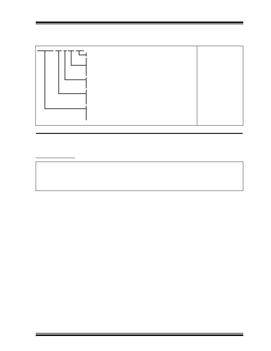
©
1997 Microchip Technology Inc.
DS30444E - page 187
PIC16C9XX
PIC16C9XX PRODUCT IDENTIFICATION SYSTEM
To order or obtain information, e.g., on pricing or delivery refer to the factory or the listed sales office.
Sales and Support
Products supported by a preliminary Data Sheet may possibly have an errata sheet describing minor operational differences and
recommended workarounds. To determine if an errata sheet exists for a particular device, please contact one of the following:
Your local Microchip sales office (see below)
The Microchip Corporate Literature Center U.S. FAX: (602) 786-7277
The Microchip's Bulletin Board, via your local CompuServe number (CompuServe membership NOT required).
Please specify which device, revision of silicon and Data Sheet (include Literature #) you are using.
For latest version information and upgrade kits for Microchip Development Tools, please call 1-800-755-2345 or 1-602-786-7302.
1.
2.
3.
* CL Devices are UV erasable and can be programmed to any device configuration. CL Devices meet the electrical requirement of
each oscillator type (including LC devices).
Pattern:
QTP, SQTP, ROM Code or Special Requirements
Package:
SP
= 64-pin Shrink PDIP
PT
= TQFP
CL
= 68-pin Windowed CERQUAD
L
= PLCC
Temperature
Range:
-
= 0
°
C to +70
°
C (T for Tape/Reel)
I
= -40
°
C to +85
°
C (S for Tape/Reel)
Frequency
Range:
04
= 200 kHz (PIC16C9XX-04)
04
= 4 MHz
08
= 8 MHz
Device
PIC16C9XX
:
V
DD
range 4.0V to 6.0V
PIC16C9XXT :
V
DD
range 4.0V to 6.0V (Tape/Reel)
PIC16LC9XX :
V
DD
range 2.5V to 6.0V
PIC16LC9XT :
V
DD
range 2.5V to 6.0V (Tape/Reel)
PART NO. -XX X /XX XXX
Examples
a)
PIC16C924 - 04/P 301
Commercial Temp.,
PDIP Package, 4 MHz,
normal V
DD
limits, QTP
pattern #301
b)
PIC16LC923 - 04/PT
Commercial Temp.,
TQFP package, 4 MHz,
extended V
DD
limits
c)
PIC16C923 - 08I/CL
Industrial Temp.,
Windowed CERQUAD
package, 8 MHz, normal
V
DD
limits

PIC16C9XX
DS30444E page 188
©
1997 Microchip Technology Inc.
Information contained in this publication regarding device applications and the like is intended for suggestion only and may be superseded by updates. No representation or
warranty is given and no liability is assumed by Microchip Technology Incorporated with respect to the accuracy or use of such information, or infringement of patents or other
intellectual property rights arising from such use or otherwise. Use of Microchip's products as critical components in life support systems is not authorized except with express
written approval by Microchip. No licenses are conveyed, implicitly or otherwise, under any intellectual property rights. The Microchip logo and name are registered trademarks
of Microchip Technology Inc. in the U.S.A. and other countries. All rights reserved. All other trademarks mentioned herein are the property of their respective companies.
DS30444E-page 189
©
1997 Microchip Technology Inc.
AMERICAS
Corporate Office
Microchip Technology Inc.
2355 West Chandler Blvd.
Chandler, AZ 85224-6199
Tel: 602-786-7200 Fax: 602-786-7277
Technical Support: 602 786-7627
Web: http://www.microchip.com
Atlanta
Microchip Technology Inc.
500 Sugar Mill Road, Suite 200B
Atlanta, GA 30350
Tel: 770-640-0034 Fax: 770-640-0307
Boston
Microchip Technology Inc.
5 Mount Royal Avenue
Marlborough, MA 01752
Tel: 508-480-9990 Fax: 508-480-8575
Chicago
Microchip Technology Inc.
333 Pierce Road, Suite 180
Itasca, IL 60143
Tel: 630-285-0071 Fax: 630-285-0075
Dallas
Microchip Technology Inc.
14651 Dallas Parkway, Suite 816
Dallas, TX 75240-8809
Tel: 972-991-7177 Fax: 972-991-8588
Dayton
Microchip Technology Inc.
Two Prestige Place, Suite 150
Miamisburg, OH 45342
Tel: 937-291-1654 Fax: 937-291-9175
Los Angeles
Microchip Technology Inc.
18201 Von Karman, Suite 1090
Irvine, CA 92612
Tel: 714-263-1888 Fax: 714-263-1338
New York
Microchip Technology Inc.
150 Motor Parkway, Suite 416
Hauppauge, NY 11788
Tel: 516-273-5305 Fax: 516-273-5335
San Jose
Microchip Technology Inc.
2107 North First Street, Suite 590
San Jose, CA 95131
Tel: 408-436-7950 Fax: 408-436-7955
Toronto
Microchip Technology Inc.
5925 Airport Road, Suite 200
Mississauga, Ontario L4V 1W1, Canada
Tel: 905-405-6279 Fax: 905-405-6253
ASIA/PACIFIC
Hong Kong
Microchip Asia Pacific
RM 3801B, Tower Two
Metroplaza
223 Hing Fong Road
Kwai Fong, N.T., Hong Kong
Tel: 852-2-401-1200 Fax: 852-2-401-3431
India
Microchip Technology Inc.
India Liaison Office
No. 6, Legacy, Convent Road
Bangalore 560 025, India
Tel: 91-80-229-4036 Fax: 91-80-559-9840
Korea
Microchip Technology Korea
168-1, Youngbo Bldg. 3 Floor
Samsung-Dong, Kangnam-Ku
Seoul, Korea
Tel: 82-2-554-7200 Fax: 82-2-558-5934
Shanghai
Microchip Technology
RM 406 Shanghai Golden Bridge Bldg.
2077 Yan'an Road West, Hong Qiao District
Shanghai, PRC 200335
Tel: 86-21-6275-5700
Fax: 86 21-6275-5060
Singapore
Microchip Technology Taiwan
Singapore Branch
200 Middle Road
#10-03 Prime Centre
Singapore 188980
Tel: 65-334-8870 Fax: 65-334-8850
Taiwan, R.O.C
Microchip Technology Taiwan
10F-1C 207
Tung Hua North Road
Taipei, Taiwan, ROC
Tel: 886 2-717-7175 Fax: 886-2-545-0139
EUROPE
United Kingdom
Arizona Microchip Technology Ltd.
Unit 6, The Courtyard
Meadow Bank, Furlong Road
Bourne End, Buckinghamshire SL8 5AJ
Tel: 44-1628-851077 Fax: 44-1628-850259
France
Arizona Microchip Technology SARL
Zone Industrielle de la Bonde
2 Rue du Buisson aux Fraises
91300 Massy, France
Tel: 33-1-69-53-63-20 Fax: 33-1-69-30-90-79
Germany
Arizona Microchip Technology GmbH
Gustav-Heinemann-Ring 125
D-81739 Müchen, Germany
Tel: 49-89-627-144 0 Fax: 49-89-627-144-44
Italy
Arizona Microchip Technology SRL
Centro Direzionale Colleoni
Palazzo Taurus 1 V. Le Colleoni 1
20041 Agrate Brianza
Milan, Italy
Tel: 39-39-6899939 Fax: 39-39-6899883
JAPAN
Microchip Technology Intl. Inc.
Benex S-1 6F
3-18-20, Shinyokohama
Kohoku-Ku, Yokohama-shi
Kanagawa 222 Japan
Tel: 81-45-471- 6166 Fax: 81-45-471-6122
7/29/97
Printed on recycled paper.
All rights reserved. ©1997, Microchip Technology Incorporated, USA. 8/97
M
W
ORLDWIDE
S
ALES
& S
ERVICE
Document Outline