 | –≠–ª–µ–∫—Ç—Ä–æ–Ω–Ω—ã–π –∫–æ–º–ø–æ–Ω–µ–Ω—Ç: PIC17C42A | –°–∫–∞—á–∞—Ç—å:  PDF PDF  ZIP ZIP |

©
1996 Microchip Technology Inc.
DS30412C-page 1
Devices included in this data sheet:
∑ PIC17CR42
∑ PIC17C42A
∑ PIC17C43
∑ PIC17CR43
∑ PIC17C44
∑ PIC17C42
Microcontroller Core Features:
∑ Only 58 single word instructions to learn
∑ All single cycle instructions (121 ns) except for
program branches and table reads/writes which
are two-cycle
∑ Operating speed:
- DC - 33 MHz clock input
- DC - 121 ns instruction cycle
∑ Hardware Multiplier
(Not available on the PIC17C42)
∑ Interrupt capability
∑ 16 levels deep hardware stack
∑ Direct, indirect and relative addressing modes
∑ Internal/External program memory execution
∑ 64K x 16 addressable program memory space
Peripheral Features:
∑ 33 I/O pins with individual direction control
∑ High current sink/source for direct LED drive
- RA2 and RA3 are open drain, high voltage
(12V), high current (60 mA), I/O
∑ Two capture inputs and two PWM outputs
- Captures are 16-bit, max resolution 160 ns
- PWM resolution is 1- to 10-bit
∑ TMR0: 16-bit timer/counter with 8-bit programma-
ble prescaler
∑ TMR1: 8-bit timer/counter
Device
Program Memory
Data Memory
EPROM
ROM
PIC17CR42
-
2K
232
PIC17C42A
2K
-
232
PIC17C43
4K
-
454
PIC17CR43
-
4K
454
PIC17C44
8K
-
454
PIC17C42
2K
-
232
B
B
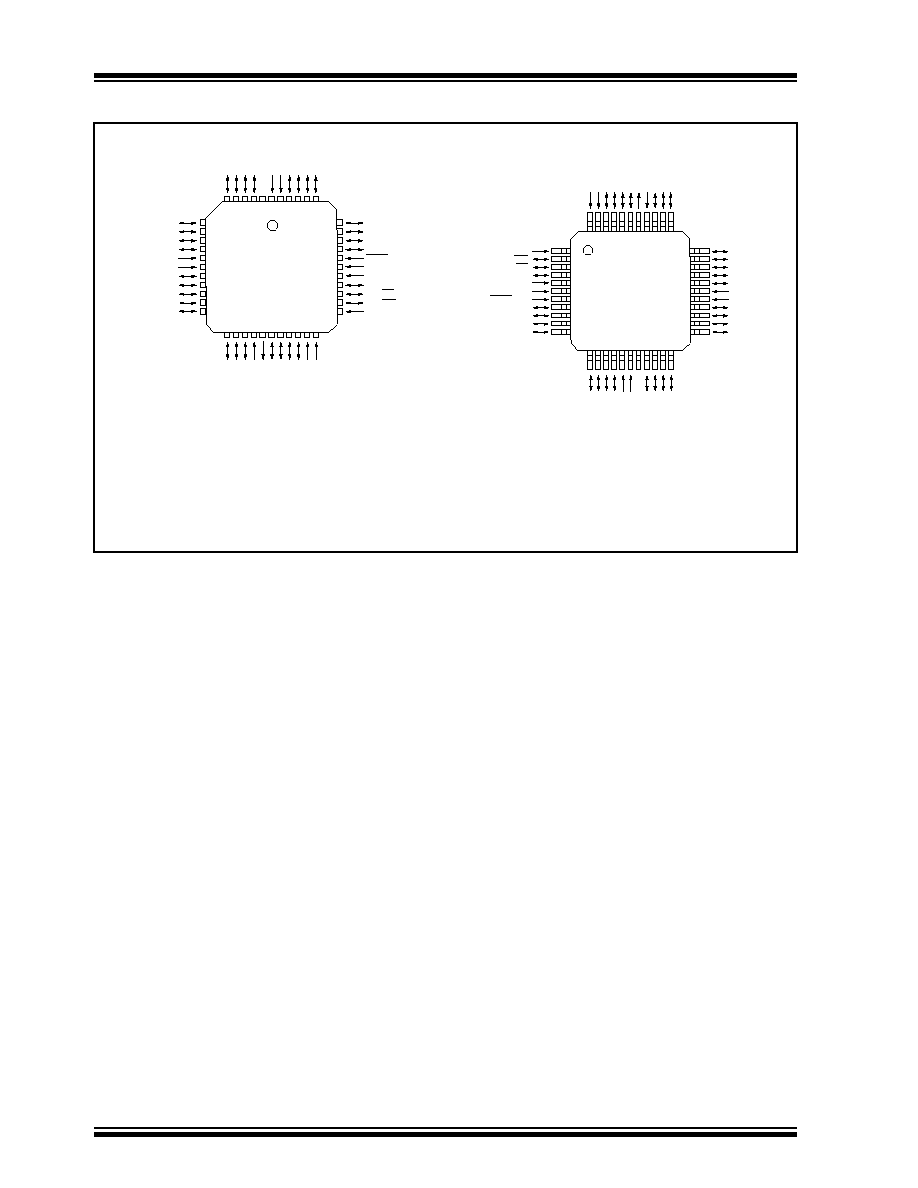
Pin Diagram
∑ TMR2: 8-bit timer/counter
∑ TMR3: 16-bit timer/counter
∑ Universal Synchronous Asynchronous Receiver
Transmitter (USART/SCI)
Special Microcontroller Features:
∑ Power-on Reset (POR), Power-up Timer (PWRT)
and Oscillator Start-up Timer (OST)
∑ Watchdog Timer (WDT) with its own on-chip RC
oscillator for reliable operation
∑ Code-protection
∑ Power saving SLEEP mode
∑ Selectable oscillator options
CMOS Technology:
∑ Low-power, high-speed CMOS EPROM/ROM
technology
∑ Fully static design
∑ Wide operating voltage range (2.5V to 6.0V)
∑ Commercial and Industrial Temperature Range
∑ Low-power consumption
- < 5 mA @ 5V, 4 MHz
- 100
µ
A typical @ 4.5V, 32 kHz
- < 1
µ
A typical standby current @ 5V
PIC17C4X
RD0/AD8
RD1/AD9
RD2/AD10
RD3/AD11
RD4/AD12
RD5/AD13
RD6/AD14
RD7/AD15
MCLR/V
PP
V
SS
RE0/ALE
RE1/OE
RE2/WR
TEST
RA0/INT
RA1/T0CKI
RA2
RA3
RA4/RX/DT
RA5/TX/CK
V
DD
RC0/AD0
RC1/AD1
RC2/AD2
RC3/AD3
RC4/AD4
RC5/AD5
RC6/AD6
RC7/AD7
V
SS
RB0/CAP1
RB1/CAP2
RB2/PWM1
RB3/PWM2
RB4/TCLK12
RB5/TCLK3
RB6
RB7
OSC1/CLKIN
OSC2/CLKOUT
1
2
3
4
5
6
7
8
9
10
11
12
13
14
15
16
17
18
19
20
40
39
38
37
36
35
34
33
32
31
30
29
28
27
26
25
24
23
22
21
PDIP, CERDIP, Windowed CERDIP
PIC17C4X
High-Performance 8-Bit CMOS EPROM/ROM Microcontroller
NOT recommended for new designs, use 17C42A.
This document was created with FrameMaker 4 0 4
PIC17C4X
DS30412C-page 2
©
1996 Microchip Technology Inc.
Pin Diagrams Cont.'d
RD4/AD12
RD5/AD13
RD6/AD14
RD7/AD15
MCLR/V
PP
V
SS
V
SS
RE0/ALE
RE1/OE
RE2/WR
TEST
RC4/AD4
RC5/AD5
RC6/AD6
RC7/AD7
V
SS
V
SS
RB0/CAP1
RB1/CAP2
RB2/PWM1
RB3/PWM2
RB4/TCLK12
RC3/AD3
RC2/AD2
RC1/AD1
RC0/AD0
NC
V
DD
V
DD
RD0/AD8
RD1/AD9
RD2/AD10
RD3/AD11
7
8
9
10
11
12
13
14
15
16
17
39
38
37
36
35
34
33
32
31
30
29
RA0/INT
RA1/T0CKI
RA2
RA3
RA4/RX/DT
RA5/TX/CK
OSC2/CLK
OUT
OSC1/CLKIN
RB7
RB6
RB5/TCLK3
6
5
4
3
2
1
44
43
42
41
40
28
27
26
25
24
23
22
21
20
19
18
RB4/TCLK12
RB3/PWM2
RB2/PWM1
RB1/CAP2
RB0/CAP1
V
SS
V
SS
RC7/AD7
RC6/AD6
RC5/AD5
RC4/AD4
TEST
RE2/WR
RE1/OE
RE0/ALE
V
SS
V
SS
MCLR/V
PP
RD7/AD15
RD6/AD14
RD5/AD13
RD4/AD12
RA0/INT
RA1/T0CKI
RA2
RA3
RA4/RX/DT
RA5/TX/CK
OSC2/CLK
OUT
OSC1/CLKIN
RB7
RB6
RB5/TCLK3
1
2
3
4
5
6
7
8
9
10
11
33
32
31
30
29
28
27
26
25
24
23
RC3/AD3
RC2/AD2
RC1/AD1
RC0/AD0
NC
V
DD
V
DD
RD0/AD8
RD1/AD9
RD2/AD10
RD3/AD11
44
43
42
41
40
39
38
37
36
35
34
22
21
20
19
18
17
16
15
14
13
12
PLCC
MQFP
TQFP
All devices are available in all package types, listed in Section 21.0, with the following exceptions:
∑ ROM devices are not available in Windowed CERDIP Packages
∑ TQFP is not available for the PIC17C42.
PIC17C4X
PIC17C4X

©
1996 Microchip Technology Inc.
DS30412C-page 3
PIC17C4X
Table of Contents
1.0
Overview .............................................................................................................................................................. 5
2.0
PIC17C4X Device Varieties ................................................................................................................................. 7
3.0
Architectural Overview ......................................................................................................................................... 9
4.0
Reset .................................................................................................................................................................. 15
5.0
Interrupts ............................................................................................................................................................ 21
6.0
Memory Organization ......................................................................................................................................... 29
7.0
Table Reads and Table Writes........................................................................................................................... 43
8.0
Hardware Multiplier ............................................................................................................................................ 49
9.0
I/O Ports ............................................................................................................................................................. 53
10.0
Overview of Timer Resources ............................................................................................................................ 65
11.0
Timer0 ................................................................................................................................................................ 67
12.0
Timer1, Timer2, Timer3, PWMs and Captures................................................................................................... 71
13.0
Universal Synchronous Asynchronous Receiver Transmitter (USART) Module ................................................ 83
14.0
Special Features of the CPU.............................................................................................................................. 99
15.0
Instruction Set Summary .................................................................................................................................. 107
16.0
Development Support....................................................................................................................................... 143
17.0
PIC17C42 Electrical Characteristics ................................................................................................................ 147
18.0
PIC17C42 DC and AC Characteristics............................................................................................................. 163
19.0
PIC17CR42/42A/43/R43/44 Electrical Characteristics..................................................................................... 175
20.0
PIC17CR42/42A/43/R43/44 DC and AC Characteristics ................................................................................. 193
21.0
Packaging Information...................................................................................................................................... 205
Appendix A: Modifications .......................................................................................................................................... 211
Appendix B: Compatibility........................................................................................................................................... 211
Appendix C: What's New ............................................................................................................................................ 212
Appendix D: What's Changed..................................................................................................................................... 212
Appendix E: PIC16/17 Microcontrollers ...................................................................................................................... 213
Appendix F: Errata for PIC17C42 Silicon ................................................................................................................... 223
Index ............................................................................................................................................................................ 226
PIC17C4X Product Identification System .................................................................................................................... 237
For register and module descriptions in this data sheet, device legends show which devices apply to those sections.
For example, the legend below shows that some features of only the PIC17C43, PIC17CR43, PIC17C44 are described
in this section.
Applicable Devices
42 R42 42A 43 R43 44
To Our Valued Customers
We constantly strive to improve the quality of all our products and documentation. We have spent an excep-
tional amount of time to ensure that these documents are correct. However, we realize that we may have
missed a few things. If you find any information that is missing or appears in error from the previous version of
the PIC17C4X Data Sheet (Literature Number DS30412B), please use the reader response form in the back
of this data sheet to inform us. We appreciate your assistance in making this a better document.
To assist you in the use of this document, Appendix C contains a list of new information in this data sheet,
while Appendix D contains information that has changed

PIC17C4X
DS30412C-page 4
©
1996 Microchip Technology Inc.
NOTES:

©
1996 Microchip Technology Inc.
DS30412C-page 5
PIC17C4X
1.0
OVERVIEW
This data sheet covers the PIC17C4X group of the
PIC17CXX family of microcontrollers. The following
devices are discussed in this data sheet:
∑ PIC17C42
∑ PIC17CR42
∑ PIC17C42A
∑ PIC17C43
∑ PIC17CR43
∑ PIC17C44
The PIC17CR42, PIC17C42A, PIC17C43,
PIC17CR43, and PIC17C44 devices include architec-
tural enhancements over the PIC17C42. These
enhancements will be discussed throughout this data
sheet.
The PIC17C4X devices are 40/44-Pin,
EPROM/ROM-based members of the versatile
PIC17CXX family of low-cost, high-performance,
CMOS, fully-static, 8-bit microcontrollers.
All PIC16/17 microcontrollers employ an advanced
RISC architecture. The PIC17CXX has enhanced core
features, 16-level deep stack, and multiple internal and
external interrupt sources. The separate instruction and
data buses of the Harvard architecture allow a 16-bit
wide instruction word with a separate 8-bit wide data.
The two stage instruction pipeline allows all instructions
to execute in a single cycle, except for program
branches (which require two cycles). A total of 55
instructions (reduced instruction set) are available in
the PIC17C42 and 58 instructions in all the other
devices. Additionally, a large register set gives some of
the architectural innovations used to achieve a very
high performance. For mathematical intensive applica-
tions all devices, except the PIC17C42, have a single
cycle 8 x 8 Hardware Multiplier.
PIC17CXX microcontrollers typically achieve a 2:1
code compression and a 4:1 speed improvement over
other 8-bit microcontrollers in their class.
PIC17C4X devices have up to 454 bytes of RAM and
33 I/O pins. In addition, the PIC17C4X adds several
peripheral features useful in many high performance
applications including:
∑ Four timer/counters
∑ Two capture inputs
∑ Two PWM outputs
∑ A Universal Synchronous Asynchronous Receiver
Transmitter (USART)
These special features reduce external components,
thus reducing cost, enhancing system reliability and
reducing power consumption. There are four oscillator
options, of which the single pin RC oscillator provides a
low-cost solution, the LF oscillator is for low frequency
crystals and minimizes power consumption, XT is a
standard crystal, and the EC is for external clock input.
The SLEEP (power-down) mode offers additional
power saving. The user can wake-up the chip from
SLEEP through several external and internal interrupts
and device resets.
There are four configuration options for the device oper-
ational modes:
∑ Microprocessor
∑ Microcontroller
∑ Extended microcontroller
∑ Protected microcontroller
The microprocessor and extended microcontroller
modes allow up to 64K-words of external program
memory.
A highly reliable Watchdog Timer with its own on-chip
RC oscillator provides protection against software mal-
function.
Table 1-1 lists the features of the PIC17C4X devices.
A UV-erasable CERDIP-packaged version is ideal for
code development while the cost-effective One-Time
Programmable (OTP) version is suitable for production
in any volume.
The PIC17C4X fits perfectly in applications ranging
from precise motor control and industrial process con-
trol to automotive, instrumentation, and telecom appli-
cations. Other applications that require extremely fast
execution of complex software programs or the flexibil-
ity of programming the software code as one of the last
steps of the manufacturing process would also be well
suited. The EPROM technology makes customization
of application programs (with unique security codes,
combinations, model numbers, parameter storage,
etc.) fast and convenient. Small footprint package
options make the PIC17C4X ideal for applications with
space limitations that require high performance. High
speed execution, powerful peripheral features, flexible
I/O, and low power consumption all at low cost make
the PIC17C4X ideal for a wide range of embedded con-
trol applications.
1.1
Family and Upward Compatibility
Those users familiar with the PIC16C5X and
PIC16CXX families of microcontrollers will see the
architectural enhancements that have been imple-
mented. These enhancements allow the device to be
more efficient in software and hardware requirements.
Please refer to Appendix A for a detailed list of
enhancements and modifications. Code written for
PIC16C5X or PIC16CXX can be easily ported to
PIC17CXX family of devices (Appendix B).
1.2
Development Support
The PIC17CXX family is supported by a full-featured
macro assembler, a software simulator, an in-circuit
emulator, a universal programmer, a "C" compiler, and
fuzzy logic support tools.
This document was created with FrameMaker 4 0 4

PIC17C4X
DS30412C-page 6
©
1996 Microchip Technology Inc.
TABLE 1-1:
PIC17CXX FAMILY OF DEVICES
Features
PIC17C42
PIC17CR42
PIC17C42A
PIC17C43
PIC17CR43
PIC17C44
Maximum Frequency of Operation
25 MHz
33 MHz
33 MHz
33 MHz
33 MHz
33 MHz
Operating Voltage Range
4.5 - 5.5V
2.5 - 6.0V
2.5 - 6.0V
2.5 - 6.0V
2.5 - 6.0V
2.5 - 6.0V
Program Memory x16
(EPROM)
2K
-
2K
4K
-
8K
(ROM)
-
2K
-
-
4K
-
Data Memory (bytes)
232
232
232
454
454
454
Hardware Multiplier (8 x 8)
-
Yes
Yes
Yes
Yes
Yes
Timer0 (16-bit + 8-bit postscaler)
Yes
Yes
Yes
Yes
Yes
Yes
Timer1 (8-bit)
Yes
Yes
Yes
Yes
Yes
Yes
Timer2 (8-bit)
Yes
Yes
Yes
Yes
Yes
Yes
Timer3 (16-bit)
Yes
Yes
Yes
Yes
Yes
Yes
Capture inputs (16-bit)
2
2
2
2
2
2
PWM outputs (up to 10-bit)
2
2
2
2
2
2
USART/SCI
Yes
Yes
Yes
Yes
Yes
Yes
Power-on Reset
Yes
Yes
Yes
Yes
Yes
Yes
Watchdog Timer
Yes
Yes
Yes
Yes
Yes
Yes
External Interrupts
Yes
Yes
Yes
Yes
Yes
Yes
Interrupt Sources
11
11
11
11
11
11
Program Memory Code Protect
Yes
Yes
Yes
Yes
Yes
Yes
I/O Pins
33
33
33
33
33
33
I/O High Current Capabil-
ity
Source
25 mA
25 mA
25 mA
25 mA
25 mA
25 mA
Sink
25 mA
(1)
25 mA
(1)
25 mA
(1)
25 mA
(1)
25 mA
(1)
25 mA
(1)
Package Types
40-pin DIP
44-pin PLCC
44-pin MQFP
40-pin DIP
44-pin PLCC
44-pin MQFP
44-pin TQFP
40-pin DIP
44-pin PLCC
44-pin MQFP
44-pin TQFP
40-pin DIP
44-pin PLCC
44-pin MQFP
44-pin TQFP
40-pin DIP
44-pin PLCC
44-pin MQFP
44-pin TQFP
40-pin DIP
44-pin PLCC
44-pin MQFP
44-pin TQFP
Note 1:
Pins RA2 and RA3 can sink up to 60 mA.

©
1996 Microchip Technology Inc.
DS30412C-page 7
PIC17C4X
2.0
PIC17C4X DEVICE VARIETIES
A variety of frequency ranges and packaging options
are available. Depending on application and production
requirements, the proper device option can be selected
using the information in the PIC17C4X Product Selec-
tion System section at the end of this data sheet. When
placing orders, please use the "PIC17C4X Product
Identification System" at the back of this data sheet to
specify the correct part number.
For the PIC17C4X family of devices, there are four
device "types" as indicated in the device number:
1.
C
, as in PIC17
C
42. These devices have
EPROM type memory and operate over the
standard voltage range.
2.
LC
, as in PIC17
LC
42. These devices have
EPROM type memory, operate over an
extended voltage range, and reduced frequency
range.
3.
CR
, as in PIC17
CR
42. These devices have
ROM type memory and operate over the stan-
dard voltage range.
4.
LCR
, as in PIC17
LCR
42. These devices have
ROM type memory, operate over an extended
voltage range, and reduced frequency range.
2.1
UV Erasable Devices
The UV erasable version, offered in CERDIP package,
is optimal for prototype development and pilot pro-
grams.
The UV erasable version can be erased and repro-
grammed to any of the configuration modes.
Microchip's PRO MATE
TM
programmer supports pro-
gramming of the PIC17C4X. Third party programmers
also are available; refer to the
Third Party Guide
for a
list of sources.
2.2
One-Time-Programmable (OTP)
Devices
The availability of OTP devices is especially useful for
customers expecting frequent code changes and
updates.
The OTP devices, packaged in plastic packages, per-
mit the user to program them once. In addition to the
program memory, the configuration bits must also be
programmed.
2.3
Quick-Turnaround-Production (QTP)
Devices
Microchip offers a QTP Programming Service for fac-
tory production orders. This service is made available
for users who choose not to program a medium to high
quantity of units and whose code patterns have stabi-
lized. The devices are identical to the OTP devices but
with all EPROM locations and configuration options
already programmed by the factory. Certain code and
prototype verification procedures apply before produc-
tion shipments are available. Please contact your local
Microchip Technology sales office for more details.
2.4
Serialized Quick-Turnaround
Production (SQTP
SM
) Devices
Microchip offers a unique programming service where
a few user-defined locations in each device are pro-
grammed with different serial numbers. The serial num-
bers may be random, pseudo-random or sequential.
Serial programming allows each device to have a
unique number which can serve as an entry-code,
password or ID number.
ROM devices do not allow serialization information in
the program memory space.
For information on submitting ROM code, please con-
tact your regional sales office.
2.5
Read Only Memory (ROM) Devices
Microchip offers masked ROM versions of several of
the highest volume parts, thus giving customers a low
cost option for high volume, mature products.
For information on submitting ROM code, please con-
tact your regional sales office.
This document was created with FrameMaker 4 0 4

PIC17C4X
DS30412C-page 8
©
1996 Microchip Technology Inc.
NOTES:

©
1996 Microchip Technology Inc.
DS30412C-page 9
PIC17C4X
3.0
ARCHITECTURAL OVERVIEW
The high performance of the PIC17C4X can be attrib-
uted to a number of architectural features commonly
found in RISC microprocessors. To begin with, the
PIC17C4X uses a modified Harvard architecture. This
architecture has the program and data accessed from
separate memories. So the device has a program
memory bus and a data memory bus. This improves
bandwidth over traditional von Neumann architecture,
where program and data are fetched from the same
memory (accesses over the same bus). Separating
program and data memory further allows instructions to
be sized differently than the 8-bit wide data word.
PIC17C4X opcodes are 16-bits wide, enabling single
word instructions. The full 16-bit wide program memory
bus fetches a 16-bit instruction in a single cycle. A two-
stage pipeline overlaps fetch and execution of instruc-
tions. Consequently, all instructions execute in a single
cycle (121 ns @ 33 MHz), except for program branches
and two special instructions that transfer data between
program and data memory.
The PIC17C4X can address up to 64K x 16 of program
memory space.
The
PIC17C42
and
PIC17C42A
integrate 2K x 16 of
EPROM program memory on-chip, while the
PIC17CR42
has 2K x 16 of ROM program memory on-
chip.
The
PIC17C43
integrates 4K x 16 of EPROM program
memory, while the
PIC17CR43
has 4K x 16 of ROM
program memory.
The
PIC17C44
integrates 8K x 16 EPROM program
memory.
Program execution can be internal only (microcontrol-
ler or protected microcontroller mode), external only
(microprocessor mode) or both (extended microcon-
troller mode). Extended microcontroller mode does not
allow code protection.
The PIC17CXX can directly or indirectly address its
register files or data memory. All special function regis-
ters, including the Program Counter (PC) and Working
Register (WREG), are mapped in the data memory.
The PIC17CXX has an orthogonal (symmetrical)
instruction set that makes it possible to carry out any
operation on any register using any addressing mode.
This symmetrical nature and lack of `special optimal sit-
uations' make programming with the PIC17CXX simple
yet efficient. In addition, the learning curve is reduced
significantly.
One of the PIC17CXX family architectural enhance-
ments from the PIC16CXX family allows two file regis-
ters to be used in some two operand instructions. This
allows data to be moved directly between two registers
without going through the WREG register. This
increases performance and decreases program mem-
ory usage.
The PIC17CXX devices contain an 8-bit ALU and work-
ing register. The ALU is a general purpose arithmetic
unit. It performs arithmetic and Boolean functions
between data in the working register and any register
file.
The ALU is 8-bits wide and capable of addition, sub-
traction, shift, and logical operations. Unless otherwise
mentioned, arithmetic operations are two's comple-
ment in nature.
The WREG register is an 8-bit working register used for
ALU operations.
All PIC17C4X devices (except the PIC17C42) have an
8 x 8 hardware multiplier. This multiplier generates a
16-bit result in a single cycle.
Depending on the instruction executed, the ALU may
affect the values of the Carry (C), Digit Carry (DC), and
Zero (Z) bits in the STATUS register. The C and DC bits
operate as a borrow and digit borrow out bit, respec-
tively, in subtraction. See the
SUBLW
and
SUBWF
instructions for examples.
Although the ALU does not perform signed arithmetic,
the Overflow bit (OV) can be used to implement signed
math. Signed arithmetic is comprised of a magnitude
and a sign bit. The overflow bit indicates if the magni-
tude overflows and causes the sign bit to change state.
Signed math can have greater than 7-bit values (mag-
nitude), if more than one byte is used. The use of the
overflow bit only operates on bit6 (MSb of magnitude)
and bit7 (sign bit) of the value in the ALU. That is, the
overflow bit is not useful if trying to implement signed
math where the magnitude, for example, is 11-bits. If
the signed math values are greater than 7-bits (15-, 24-
or 31-bit), the algorithm must ensure that the low order
bytes ignore the overflow status bit.
Care should be taken when adding and subtracting
signed numbers to ensure that the correct operation is
executed. Example 3-1 shows an item that must be
taken into account when doing signed arithmetic on an
ALU which operates as an unsigned machine.
EXAMPLE 3-1:
SIGNED MATH
Signed math requires the result in REG to
be FEh (-126). This would be accomplished
by subtracting one as opposed to adding
one.
Simplified block diagrams are shown in Figure 3-1 and
Figure 3-2. The descriptions of the device pins are
listed in Table 3-1.
Hex Value
Signed Value
Math
Unsigned Value
Math
FFh
+ 01h
= ?
-127
+ 1
= -126 (FEh)
255
+ 1
= 0 (00h);
Carry bit = 1
This document was created with FrameMaker 4 0 4

PIC17C4X
DS30412C-page 10
©
1996 Microchip Technology Inc.
FIGURE 3-1:
PIC17C42 BLOCK DIAGRAM
CLOCK GENERA
T
O
R
PO
WER ON RESET
W
A
TCHDOG TIMER
OSC ST
AR
TUP
TIMER
TEST MODE SELECT
SYSTEM
D
A
T
A
LA
TCH
ADDRESS LA
TCH
PR
OGRAM
MEMOR
Y
(EPR
OM/R
OM)
T
ABLE PTR<16>
ST
A
C
K
16 x 16
PCH
PCL
PCLA
TH<8>
T
ABLE LA
TCH <16>
R
OM LA
TCH <16>
LITERAL
INSTR
UCTION
DECODER
CONTR
OL OUTPUTS
IR LA
TCH <16>
FSR0
FSR1
8
8
8
IR BUS <16>
RAM ADDR B
UFFER
D
A
T
A
LA
TCH
READ/WRITE
DECODE
FOR REGISTERS
MAPPED
IN D
A
T
A
SP
A
C
E
WREG <8>
BIT
OP
ALU
SHIFTER
IR BUS <16>
POR
TB
POR
T
A
RB0/CAP1
RB1/CAP2
RB2/PWM1
RB2/PWM2
RB4/TCLK12
RB5/TCLK3
RB6
RB7
RA0/INT
RA1/T0CKI
RA2
RA3
RA4/RX/DT
RA5/TX/CK
RA1/
Timer1, Timer2, Timer3
CAPTURE
PWM
DIGIT
AL I/O
POR
TS A, B
SERIAL POR
T
Timer0 MODULE
D
A
T
A
B
US <8>
IR BUS <7:0>
RA1/T0CKI
RA0/INT
86
8
6
2
6
4
3
IR <2:0>
DA
T A
BUS <8>
CONTR
OL
SIGNALS
T
O
CPU
CHIP_RESET
AND O
THER
CONTR
OL
SIGNALS
Q1, Q2, Q3, Q4
16
16
11
AD <15:0>
POR
TC and
ALE, WR
, OE
POR
TE
OSC1, OSC2
V
DD
, V
SS
MCLR
/V
PP
TEST
DECODE
BSR
INTERR
UPT
MODULE
8
RDF
WRF
T0CKI
PERIPHERALS
IR <7>
BU
S
INTER
-
FA
C
E
16
D
A
T
A
RAM
232x8
2K x 16
POR
TD

©
1996 Microchip Technology Inc.
DS30412C-page 11
PIC17C4X
FIGURE 3-2:
PIC17CR42/42A/43/R43/44 BLOCK DIAGRAM
CLOCK GENERA
T
O
R
PO
WER ON RESET
W
A
TCHDOG TIMER
OSC ST
AR
TUP
TIMER
TEST MODE SELECT
SYSTEM
D
A
T
A
LA
TCH
ADDRESS LA
TCH
PR
OGRAM
MEMOR
Y
(EPR
OM/R
OM)
T
ABLE PTR<16>
ST
A
C
K
16 x 16
PCH
PCL
PCLA
TH<8>
T
ABLE LA
TCH <16>
R
OM LA
TCH <16>
LITERAL
INSTR
UCTION
DECODER
CONTR
OL OUTPUTS
IR LA
TCH <16>
FSR0
FSR1
8
8
8
IR BUS <16>
RAM ADDR B
UFFER
D
A
T
A
LA
TCH
READ/WRITE
DECODE
FOR REGISTERS
MAPPED
IN D
A
T
A
SP
A
C
E
WREG <8>
BIT
OP
ALU
SHIFTER
IR BUS <16>
POR
TB
POR
T
A
RB0/CAP1
RB1/CAP2
RB2/PWM1
RB2/PWM2
RB4/TCLK12
RB5/TCLK3
RB6
RB7
RA0/INT
RA1/T0CKI
RA2
RA3
RA4/RX/DT
RA5/TX/CK
RA1/
Timer1, Timer2, Timer3
CAPTURE
PWM
DIGIT
AL I/O
POR
TS A, B
SERIAL POR
T
Timer0 MODULE
D
A
T
A
B
US <8>
BSR<7:4>
RA1/T0CKI
RA0/INT
86
8
6
2
6
4
3
IR <2:0>
DA
T A
BUS <8>
CONTR
OL
SIGNALS
T
O
CPU
CHIP_RESET
AND O
THER
CONTR
OL
SIGNALS
Q1, Q2, Q3, Q4
16
16
13
AD <15:0>
POR
TC and
ALE, WR
, OE
POR
TE
OSC1, OSC2
V
DD
, V
SS
MCLR
/V
PP
TEST
DECODE
BSR
INTERR
UPT
MODULE
12
RDF
WRF
T0CKI
PERIPHERALS
IR <7>
BU
S
INTER
-
FA
C
E
16
8 x 8 mult
PR
ODH
PR
ODL
D
A
T
A
RAM
454 x 8 PIC17C43
8K x 16 - PIC17C44
4K x 16 - PIC17C43
IR BUS<7:0>
4K x 16 - PIC17CR43
454 x 8 PIC17CR43
454 x 8 PIC17C44
232 x
8 PIC17C42A
232 x
8 PIC17CR42
2K x 16 - PIC17C4
2A
2K x 16 - PIC17C
R42
POR
TD

PIC17C4X
DS30412C-page 12
©
1996 Microchip Technology Inc.
TABLE 3-1:
PINOUT DESCRIPTIONS
Name
DIP
No.
PLCC
No.
QFP
No.
I/O/P
Type
Buffer
Type
Description
OSC1/CLKIN
19
21
37
I
ST
Oscillator input in crystal/resonator or RC oscillator mode.
External clock input in external clock mode.
OSC2/CLKOUT
20
22
38
O
--
Oscillator output. Connects to crystal or resonator in crystal
oscillator mode. In RC oscillator or external clock modes
OSC2 pin outputs CLKOUT which has one fourth the fre-
quency of OSC1 and denotes the instruction cycle rate.
MCLR/V
PP
32
35
7
I/P
ST
Master clear (reset) input/Programming Voltage (V
PP
) input.
This is the active low reset input to the chip.
PORTA is a bi-directional I/O Port except for RA0 and RA1
which are input only.
RA0/INT
26
28
44
I
ST
RA0/INT can also be selected as an external interrupt
input. Interrupt can be configured to be on positive or
negative edge.
RA1/T0CKI
25
27
43
I
ST
RA1/T0CKI can also be selected as an external interrupt
input, and the interrupt can be configured to be on posi-
tive or negative edge. RA1/T0CKI can also be selected
to be the clock input to the Timer0 timer/counter.
RA2
24
26
42
I/O
ST
High voltage, high current, open drain input/output port
pins.
RA3
23
25
41
I/O
ST
High voltage, high current, open drain input/output port
pins.
RA4/RX/DT
22
24
40
I/O
ST
RA4/RX/DT can also be selected as the USART (SCI)
Asynchronous Receive or USART (SCI) Synchronous
Data.
RA5/TX/CK
21
23
39
I/O
ST
RA5/TX/CK can also be selected as the USART (SCI)
Asynchronous Transmit or USART (SCI) Synchronous
Clock.
PORTB is a bi-directional I/O Port with software configurable
weak pull-ups.
RB0/CAP1
11
13
29
I/O
ST
RB0/CAP1 can also be the CAP1 input pin.
RB1/CAP2
12
14
30
I/O
ST
RB1/CAP2 can also be the CAP2 input pin.
RB2/PWM1
13
15
31
I/O
ST
RB2/PWM1 can also be the PWM1 output pin.
RB3/PWM2
14
16
32
I/O
ST
RB3/PWM2 can also be the PWM2 output pin.
RB4/TCLK12
15
17
33
I/O
ST
RB4/TCLK12 can also be the external clock input to
Timer1 and Timer2.
RB5/TCLK3
16
18
34
I/O
ST
RB5/TCLK3 can also be the external clock input to
Timer3.
RB6
17
19
35
I/O
ST
RB7
18
20
36
I/O
ST
PORTC is a bi-directional I/O Port.
RC0/AD0
2
3
19
I/O
TTL
This is also the lower half of the 16-bit wide system bus
in microprocessor mode or extended microcontroller
mode. In multiplexed system bus configuration, these
pins are address output as well as data input or output.
RC1/AD1
3
4
20
I/O
TTL
RC2/AD2
4
5
21
I/O
TTL
RC3/AD3
5
6
22
I/O
TTL
RC4/AD4
6
7
23
I/O
TTL
RC5/AD5
7
8
24
I/O
TTL
RC6/AD6
8
9
25
I/O
TTL
RC7/AD7
9
10
26
I/O
TTL
Legend: I = Input only; O = Output only; I/O = Input/Output; P = Power; -- = Not Used; TTL = TTL input;
ST = Schmitt Trigger input.

©
1996 Microchip Technology Inc.
DS30412C-page 13
PIC17C4X
PORTD is a bi-directional I/O Port.
RD0/AD8
40
43
15
I/O
TTL
This is also the upper byte of the 16-bit system bus in
microprocessor mode or extended microprocessor mode
or extended microcontroller mode. In multiplexed system
bus configuration these pins are address output as well
as data input or output.
RD1/AD9
39
42
14
I/O
TTL
RD2/AD10
38
41
13
I/O
TTL
RD3/AD11
37
40
12
I/O
TTL
RD4/AD12
36
39
11
I/O
TTL
RD5/AD13
35
38
10
I/O
TTL
RD6/AD14
34
37
9
I/O
TTL
RD7/AD15
33
36
8
I/O
TTL
PORTE is a bi-directional I/O Port.
RE0/ALE
30
32
4
I/O
TTL
In microprocessor mode or extended microcontroller
mode, it is the Address Latch Enable (ALE) output.
Address should be latched on the falling edge of ALE
output.
RE1/OE
29
31
3
I/O
TTL
In microprocessor or extended microcontroller mode, it is
the Output Enable (OE) control output (active low).
RE2/WR
28
30
2
I/O
TTL
In microprocessor or extended microcontroller mode, it is
the Write Enable (WR) control output (active low).
TEST
27
29
1
I
ST
Test mode selection control input. Always tie to V
SS
for nor-
mal operation.
V
SS
10,
31
11,
12,
33, 34
5, 6,
27, 28
P
Ground reference for logic and I/O pins.
V
DD
1
1, 44
16, 17
P
Positive supply for logic and I/O pins.
TABLE 3-1:
PINOUT DESCRIPTIONS
Name
DIP
No.
PLCC
No.
QFP
No.
I/O/P
Type
Buffer
Type
Description
Legend: I = Input only; O = Output only; I/O = Input/Output; P = Power; -- = Not Used; TTL = TTL input;
ST = Schmitt Trigger input.

PIC17C4X
DS30412C-page 14
©
1996 Microchip Technology Inc.
3.1
Clocking Scheme/Instruction Cycle
The clock input (from OSC1) is internally divided by
four to generate four non-overlapping quadrature
clocks, namely Q1, Q2, Q3, and Q4. Internally, the pro-
gram counter (PC) is incremented every Q1, and the
instruction is fetched from the program memory and
latched into the instruction register in Q4. The instruc-
tion is decoded and executed during the following Q1
through Q4. The clocks and instruction execution flow
are shown in Figure 3-3.
3.2
Instruction Flow/Pipelining
An "Instruction Cycle" consists of four Q cycles (Q1,
Q2, Q3, and Q4). The instruction fetch and execute are
pipelined such that fetch takes one instruction cycle
while decode and execute takes another instruction
cycle. However, due to the pipelining, each instruction
effectively executes in one cycle. If an instruction
causes the program counter to change (e.g.
GOTO
) then
two cycles are required to complete the instruction
(Example 3-2).
A fetch cycle begins with the program counter incre-
menting in Q1.
In the execution cycle, the fetched instruction is latched
into the "Instruction Register (IR)" in cycle Q1. This
instruction is then decoded and executed during the
Q2, Q3, and Q4 cycles. Data memory is read during Q2
(operand read) and written during Q4 (destination
write).
FIGURE 3-3:
CLOCK/INSTRUCTION CYCLE
EXAMPLE 3-2:
INSTRUCTION PIPELINE FLOW
Q1
Q2
Q3
Q4
Q1
Q2
Q3
Q4
Q1
Q2
Q3
Q4
OSC1
Q1
Q2
Q3
Q4
PC
OSC2/CLKOUT
(RC mode)
PC
PC+1
PC+2
Fetch INST (PC)
Execute INST (PC-1)
Fetch INST (PC+1)
Execute INST (PC)
Fetch INST (PC+2)
Execute INST (PC+1)
Internal
phase
clock
All instructions are single cycle, except for any program branches. These take two cycles since the fetch
instruction is "flushed" from the pipeline while the new instruction is being fetched and then executed.
Tcy0
Tcy1
Tcy2
Tcy3
Tcy4
Tcy5
1. MOVLW 55h
Fetch 1
Execute 1
2. MOVWF PORTB
Fetch 2
Execute 2
3. CALL SUB_1
Fetch 3
Execute 3
4. BSF PORTA, BIT3 (Forced NOP)
Fetch 4
Flush
5. Instruction @ address SUB_1
Fetch SUB_1 Execute SUB_1

©
1996 Microchip Technology Inc.
DS30412C-page 15
PIC17C4X
4.0
RESET
The PIC17CXX differentiates between various kinds of
reset:
∑ Power-on Reset (POR)
∑ MCLR reset during normal operation
∑ WDT Reset (normal operation)
Some registers are not affected in any reset condition;
their status is unknown on POR and unchanged in any
other reset. Most other registers are forced to a "reset
state" on Power-on Reset (POR), on MCLR or WDT
Reset and on MCLR reset during SLEEP. They are not
affected by a WDT Reset during SLEEP, since this reset
is viewed as the resumption of normal operation. The
TO and PD bits are set or cleared differently in different
reset situations as indicated in Table 4-3. These bits are
used in software to determine the nature of reset. See
Table 4-4 for a full description of reset states of all reg-
isters.
A simplified block diagram of the on-chip reset circuit is
shown in Figure 4-1.
Note:
While the device is in a reset state, the
internal phase clock is held in the Q1 state.
Any processor mode that allows external
execution will force the RE0/ALE pin as a
low output and the RE1/OE and RE2/WR
pins as high outputs.
4.1
Power-on Reset (POR), Power-up
Timer (PWRT), and Oscillator Start-up
Timer (OST)
4.1.1
POWER-ON RESET (POR)
The Power-on Reset circuit holds the device in reset
until V
DD
is above the trip point (in the range of 1.4V -
2.3V). The PIC17C42 does not produce an internal
reset when V
DD
declines. All other devices will produce
an internal reset for both rising and falling V
DD
. To take
advantage of the POR, just tie the MCLR/V
PP
pin
directly (or through a resistor) to V
DD
. This will eliminate
external RC components usually needed to create
Power-on Reset. A minimum rise time for V
DD
is
required. See Electrical Specifications for details.
4.1.2
POWER-UP TIMER (PWRT)
The Power-up Timer provides a fixed 96 ms time-out
(nominal) on power-up. This occurs from rising edge of
the POR signal and after the first rising edge of MCLR
(detected high). The Power-up Timer operates on an
internal RC oscillator. The chip is kept in RESET as
long as the PWRT is active. In most cases the PWRT
delay allows the V
DD
to rise to an acceptable level.
The power-up time delay will vary from chip to chip and
to V
DD
and temperature. See DC parameters for
details.
FIGURE 4-1:
SIMPLIFIED BLOCK DIAGRAM OF ON-CHIP RESET CIRCUIT
S
R
Q
External
Reset
MCLR
V
DD
OSC1
WDT
Module
V
DD
rise
detect
OST/PWRT
On-chip
RC OSC
WDT
Time_Out
Power_On_Reset
OST
10-bit Ripple counter
PWRT
Chip_Reset
10-bit Ripple counter
Power_Up
(Enable the PWRT timer
only during Power_Up)
(Power_Up + Wake_Up) (XT + LF)
(Enable the OST if it is Power_Up or Wake_Up
from SLEEP and OSC type is XT or LF)
Reset
Enab
le OST
Enab
le PWR
T
This RC oscillator is shared with the WDT
when not in a power-up sequence.
This document was created with FrameMaker 4 0 4

PIC17C4X
DS30412C-page 16
©
1996 Microchip Technology Inc.
4.1.3
OSCILLATOR START-UP TIMER (OST)
The Oscillator Start-up Timer (OST) provides a 1024
oscillator cycle (1024T
OSC
) delay after MCLR is
detected high or a wake-up from SLEEP event occurs.
The OST time-out is invoked only for XT and LF oscilla-
tor modes on a Power-on Reset or a Wake-up from
SLEEP.
The OST counts the oscillator pulses on the
OSC1/CLKIN pin. The counter only starts incrementing
after the amplitude of the signal reaches the oscillator
input thresholds. This delay allows the crystal oscillator
or resonator to stabilize before the device exits reset.
The length of time-out is a function of the crystal/reso-
nator frequency.
4.1.4
TIME-OUT SEQUENCE
On power-up the time-out sequence is as follows: First
the internal POR signal goes high when the POR trip
point is reached. If MCLR is high, then both the OST
and PWRT timers start. In general the PWRT time-out
is longer, except with low frequency crystals/resona-
tors. The total time-out also varies based on oscillator
configuration. Table 4-1 shows the times that are asso-
ciated with the oscillator configuration. Figure 4-2 and
Figure 4-3 display these time-out sequences.
If the device voltage is not within electrical specification
at the end of a time-out, the MCLR/V
PP
pin must be
held low until the voltage is within the device specifica-
tion. The use of an external RC delay is sufficient for
many of these applications.
TABLE 4-1:
TIME-OUT IN VARIOUS
SITUATIONS
The time-out sequence begins from the first rising edge
of MCLR.
Table 4-3 shows the reset conditions for some special
registers, while Table 4-4 shows the initialization condi-
tions for all the registers. The shaded registers (in
Table 4-4) are for all devices except the PIC17C42. In
the PIC17C42, the PRODH and PRODL registers are
general purpose RAM.
TABLE 4-2:
STATUS BITS AND THEIR
SIGNIFICANCE
In Figure 4-2, Figure 4-3 and Figure 4-4, T
PWRT
>
T
OST
, as would be the case in higher frequency crys-
tals. For lower frequency crystals, (i.e., 32 kHz) T
OST
would be greater.
Oscillator
Configuration
Power-up
Wake up
from
SLEEP
MCLR
Reset
XT, LF
Greater of:
96 ms or
1024T
OSC
1024T
OSC
--
EC, RC
Greater of:
96 ms or
1024T
OSC
--
--
TO
PD
Event
1
1
Power-on Reset, MCLR Reset during normal
operation, or
CLRWDT
instruction executed
1
0
MCLR Reset during SLEEP or interrupt wake-up
from SLEEP
0
1
WDT Reset during normal operation
0
0
WDT Reset during SLEEP
TABLE 4-3:
RESET CONDITION FOR THE PROGRAM COUNTER AND THE CPUSTA REGISTER
Event
PCH:PCL
CPUSTA
OST Active
Power-on Reset
0000h
--11 11--
Yes
MCLR Reset during normal operation
0000h
--11 11--
No
MCLR Reset during SLEEP
0000h
--11 10--
Yes
(2)
WDT Reset during normal operation
0000h
--11 01--
No
WDT Reset during SLEEP
(3)
0000h
--11 00--
Yes
(2)
Interrupt wake-up from SLEEP
GLINTD is set
PC + 1
--11 10--
Yes
(2)
GLINTD is clear
PC + 1
(1)
--10 10--
Yes
(2)
Legend:
u
= unchanged,
x
= unknown,
-
= unimplemented read as '0'.
Note 1: On wake-up, this instruction is executed. The instruction at the appropriate interrupt vector is fetched and
then executed.
2: The OST is only active when the Oscillator is configured for XT or LF modes.
3: The Program Counter = 0, that is the device branches to the reset vector. This is different from the
mid-range devices.

©
1996 Microchip Technology Inc.
DS30412C-page 17
PIC17C4X
FIGURE 4-2:
TIME-OUT SEQUENCE ON POWER-UP (MCLR TIED TO V
DD
)
FIGURE 4-3:
TIME-OUT SEQUENCE ON POWER-UP (MCLR NOT TIED TO V
DD
)
FIGURE 4-4:
SLOW RISE TIME (MCLR TIED TO V
DD
)
T
PWRT
T
OST
V
DD
MCLR
INTERNAL POR
PWRT TIME-OUT
OST TIME-OUT
INTERNAL RESET
T
PWRT
T
OST
V
DD
MCLR
INTERNAL POR
PWRT TIME-OUT
OST TIME-OUT
INTERNAL RESET
V
DD
MCLR
INTERNAL POR
PWRT TIME-OUT
OST TIME-OUT
INTERNAL RESET
0V
1V
5V
T
PWRT
T
OST

PIC17C4X
DS30412C-page 18
©
1996 Microchip Technology Inc.
FIGURE 4-5:
OSCILLATOR START-UP TIME
FIGURE 4-6:
USING ON-CHIP POR
FIGURE 4-7:
BROWN-OUT PROTECTION
CIRCUIT 1
V
DD
MCLR
OSC2
OST TIME_OUT
PWRT TIME_OUT
INTERNAL RESET
T
OSC
1
T
OST
T
PWRT
This figure shows in greater detail the timings involved
with the oscillator start-up timer. In this example the
low frequency crystal start-up time is larger than
power-up time (T
PWRT
).
Tosc1 = time for the crystal oscillator to react to an
oscillation level detectable by the Oscillator Start-up
Timer (ost).
T
OST
= 1024T
OSC
.
V
DD
MCLR
PIC17CXX
V
DD
This circuit will activate reset when V
DD
goes below
(Vz + 0.7V) where Vz = Zener voltage.
V
DD
33k
10k
40 k
V
DD
MCLR
PIC17CXX
FIGURE 4-8:
PIC17C42 EXTERNAL
POWER-ON RESET CIRCUIT
(FOR SLOW V
DD
POWER-UP)
FIGURE 4-9:
BROWN-OUT PROTECTION
CIRCUIT 2
Note 1: An external Power-on Reset circuit is
required only if V
DD
power-up time is too
slow. The diode D helps discharge the
capacitor quickly when V
DD
powers
down.
2: R < 40 k
is recommended to ensure
that the voltage drop across R does not
exceed 0.2V (max. leakage current spec.
on the MCLR/V
PP
pin is 5
µ
A). A larger
voltage drop will degrade V
IH
level on the
MCLR/V
PP
pin.
3: R1 = 100
to 1 k
will limit any current
flowing into MCLR from external capaci-
tor C in the event of MCLR/V
PP
pin
breakdown due to Electrostatic Dis-
charge (ESD) or (Electrical Overstress)
EOS.
C
R1
R
D
V
DD
MCLR
PIC17C42
V
DD
This brown-out circuit is less expensive, albeit less
accurate. Transistor Q1 turns off when V
DD
is below a
certain level such that:
V
DD
∑
R1
R1 + R2
= 0.7V
R2
40 k
V
DD
MCLR
PIC17CXX
R1
Q1
V
DD

©
1996 Microchip Technology Inc.
DS30412C-page 19
PIC17C4X
TABLE 4-4:
INITIALIZATION CONDITIONS FOR SPECIAL FUNCTION REGISTERS
Register
Address
Power-on Reset
MCLR Reset
WDT Reset
Wake-up from SLEEP
through interrupt
Unbanked
INDF0
00h
0000 0000
0000 0000
0000 0000
FSR0
01h
xxxx xxxx
uuuu uuuu
uuuu uuuu
PCL
02h
0000h
0000h
PC + 1
(2)
PCLATH
03h
0000 0000
0000 0000
uuuu uuuu
ALUSTA
04h
1111 xxxx
1111 uuuu
1111 uuuu
T0STA
05h
0000 000-
0000 000-
0000 000-
CPUSTA
(3)
06h
--11 11--
--11 qq--
--uu qq--
INTSTA
07h
0000 0000
0000 0000
uuuu uuuu
(1)
INDF1
08h
0000 0000
0000 0000
uuuu uuuu
FSR1
09h
xxxx xxxx
uuuu uuuu
uuuu uuuu
WREG
0Ah
xxxx xxxx
uuuu uuuu
uuuu uuuu
TMR0L
0Bh
xxxx xxxx
uuuu uuuu
uuuu uuuu
TMR0H
0Ch
xxxx xxxx
uuuu uuuu
uuuu uuuu
TBLPTRL
(4)
0Dh
xxxx xxxx
uuuu uuuu
uuuu uuuu
TBLPTRH
(4)
0Eh
xxxx xxxx
uuuu uuuu
uuuu uuuu
TBLPTRL
(5)
0Dh
0000 0000
0000 0000
uuuu uuuu
TBLPTRH
(5)
0Eh
0000 0000
0000 0000
uuuu uuuu
BSR
0Fh
0000 0000
0000 0000
uuuu uuuu
Bank 0
PORTA
10h
0-xx xxxx
0-uu uuuu
uuuu uuuu
DDRB
11h
1111 1111
1111 1111
uuuu uuuu
PORTB
12h
xxxx xxxx
uuuu uuuu
uuuu uuuu
RCSTA
13h
0000 -00x
0000 -00u
uuuu -uuu
RCREG
14h
xxxx xxxx
uuuu uuuu
uuuu uuuu
TXSTA
15h
0000 --1x
0000 --1u
uuuu --uu
TXREG
16h
xxxx xxxx
uuuu uuuu
uuuu uuuu
SPBRG
17h
xxxx xxxx
uuuu uuuu
uuuu uuuu
Bank 1
DDRC
10h
1111 1111
1111 1111
uuuu uuuu
PORTC
11h
xxxx xxxx
uuuu uuuu
uuuu uuuu
DDRD
12h
1111 1111
1111 1111
uuuu uuuu
PORTD
13h
xxxx xxxx
uuuu uuuu
uuuu uuuu
DDRE
14h
---- -111
---- -111
---- -uuu
PORTE
15h
---- -xxx
---- -uuu
---- -uuu
PIR
16h
0000 0010
0000 0010
uuuu uuuu
(1)
PIE
17h
0000 0000
0000 0000
uuuu uuuu
Legend:
u
= unchanged,
x
= unknown,
-
= unimplemented read as '0',
q
= value depends on condition.
Note 1: One or more bits in INTSTA, PIR will be affected (to cause wake-up).
2: When the wake-up is due to an interrupt and the GLINTD bit is cleared, the PC is loaded with the interrupt
vector.
3: See Table 4-3 for reset value of specific condition.
4: Only applies to the PIC17C42.
5: Does not apply to the PIC17C42.

PIC17C4X
DS30412C-page 20
©
1996 Microchip Technology Inc.
Bank 2
TMR1
10h
xxxx xxxx
uuuu uuuu
uuuu uuuu
TMR2
11h
xxxx xxxx
uuuu uuuu
uuuu uuuu
TMR3L
12h
xxxx xxxx
uuuu uuuu
uuuu uuuu
TMR3H
13h
xxxx xxxx
uuuu uuuu
uuuu uuuu
PR1
14h
xxxx xxxx
uuuu uuuu
uuuu uuuu
PR2
15h
xxxx xxxx
uuuu uuuu
uuuu uuuu
PR3/CA1L
16h
xxxx xxxx
uuuu uuuu
uuuu uuuu
PR3/CA1H
17h
xxxx xxxx
uuuu uuuu
uuuu uuuu
Bank 3
PW1DCL
10h
xx-- ----
uu-- ----
uu-- ----
PW2DCL
11h
xx-- ----
uu-- ----
uu-- ----
PW1DCH
12h
xxxx xxxx
uuuu uuuu
uuuu uuuu
PW2DCH
13h
xxxx xxxx
uuuu uuuu
uuuu uuuu
CA2L
14h
xxxx xxxx
uuuu uuuu
uuuu uuuu
CA2H
15h
xxxx xxxx
uuuu uuuu
uuuu uuuu
TCON1
16h
0000 0000
0000 0000
uuuu uuuu
TCON2
17h
0000 0000
0000 0000
uuuu uuuu
Unbanked
PRODL
(5)
18h
xxxx xxxx
uuuu uuuu
uuuu uuuu
PRODH
(5)
19h
xxxx xxxx
uuuu uuuu
uuuu uuuu
TABLE 4-4:
INITIALIZATION CONDITIONS FOR SPECIAL FUNCTION REGISTERS (Cont.'d)
Register
Address
Power-on Reset
MCLR Reset
WDT Reset
Wake-up from SLEEP
through interrupt
Legend:
u
= unchanged,
x
= unknown,
-
= unimplemented read as '0',
q
= value depends on condition.
Note 1: One or more bits in INTSTA, PIR will be affected (to cause wake-up).
2: When the wake-up is due to an interrupt and the GLINTD bit is cleared, the PC is loaded with the interrupt
vector.
3: See Table 4-3 for reset value of specific condition.
4: Only applies to the PIC17C42.
5: Does not apply to the PIC17C42.

©
1996 Microchip Technology Inc.
DS30412C-page 21
PIC17C4X
5.0
INTERRUPTS
The PIC17C4X devices have 11 sources of interrupt:
∑ External interrupt from the RA0/INT pin
∑ Change on RB7:RB0 pins
∑ TMR0 Overflow
∑ TMR1 Overflow
∑ TMR2 Overflow
∑ TMR3 Overflow
∑ USART Transmit buffer empty
∑ USART Receive buffer full
∑ Capture1
∑ Capture2
∑ T0CKI edge occurred
There are four registers used in the control and status
of interrupts. These are:
∑ CPUSTA
∑ INTSTA
∑ PIE
∑ PIR
The CPUSTA register contains the GLINTD bit. This is
the Global Interrupt Disable bit. When this bit is set, all
interrupts are disabled. This bit is part of the controller
core functionality and is described in the Memory Orga-
nization section.
When an interrupt is responded to, the GLINTD bit is
automatically set to disable any further interrupt, the
return address is pushed onto the stack and the PC is
loaded with the interrupt vector address. There are four
interrupt vectors. Each vector address is for a specific
interrupt source (except the peripheral interrupts which
have the same vector address). These sources are:
∑ External interrupt from the RA0/INT pin
∑ TMR0 Overflow
∑ T0CKI edge occurred
∑ Any peripheral interrupt
When program execution vectors to one of these inter-
rupt vector addresses (except for the peripheral inter-
rupt address), the interrupt flag bit is automatically
cleared. Vectoring to the peripheral interrupt vector
address does not automatically clear the source of the
interrupt. In the peripheral interrupt service routine, the
source(s) of the interrupt can be determined by testing
the interrupt flag bits. The interrupt flag bit(s) must be
cleared in software before re-enabling interrupts to
avoid infinite interrupt requests.
All of the individual interrupt flag bits will be set regard-
less of the status of their corresponding mask bit or the
GLINTD bit.
For external interrupt events, there will be an interrupt
latency. For two cycle instructions, the latency could be
one instruction cycle longer.
The "return from interrupt" instruction,
RETFIE
, can be
used to mark the end of the interrupt service routine.
When this instruction is executed, the stack is
"POPed", and the GLINTD bit is cleared (to re-enable
interrupts).
FIGURE 5-1:
INTERRUPT LOGIC
TMR1IF
TMR1IE
TMR2IF
TMR2IE
TMR3IF
TMR3IE
CA1IF
CA1IE
CA2IF
CA2IE
TXIF
TXIE
RCIF
RCIE
RBIF
RBIE
T0IF
T0IE
INTF
INTE
T0CKIF
T0CKIE
GLINTD
PEIE
Wake-up (If in SLEEP mode)
or terminate long write
Interrupt to CPU
PEIF
This document was created with FrameMaker 4 0 4

PIC17C4X
DS30412C-page 22
©
1996 Microchip Technology Inc.
5.1
Interrupt Status Register (INTSTA)
The Interrupt Status/Control register (INTSTA) records
the individual interrupt requests in flag bits, and con-
tains the individual interrupt enable bits (not for the
peripherals).
The PEIF bit is a read only, bit wise OR of all the periph-
eral flag bits in the PIR register (Figure 5-4).
Care should be taken when clearing any of the INTSTA
register enable bits when interrupts are enabled
(GLINTD is clear). If any of the INTSTA flag bits (T0IF,
INTF, T0CKIF, or PEIF) are set in the same instruction
cycle as the corresponding interrupt enable bit is
cleared, the device will vector to the reset address
(0x00).
When disabling any of the INTSTA enable bits, the
GLINTD bit should be set (disabled).
Note:
T0IF, INTF, T0CKIF, or PEIF will be set by
the specified condition, even if the corre-
sponding interrupt enable bit is clear (inter-
rupt disabled) or the GLINTD bit is set (all
interrupts disabled).
FIGURE 5-2: INTSTA REGISTER (ADDRESS: 07h, UNBANKED)
R - 0
R/W - 0 R/W - 0 R/W - 0
R/W - 0
R/W - 0
R/W - 0
R/W - 0
PEIF
T0CKIF
T0IF
INTF
PEIE
T0CKIE
T0IE
INTE
R = Readable bit
W = Writable bit
- n = Value at POR reset
bit7
bit0
bit 7:
PEIF
: Peripheral Interrupt Flag bit
This bit is the OR of all peripheral interrupt flag bits AND'ed with their corresponding enable bits.
1 = A peripheral interrupt is pending
0 = No peripheral interrupt is pending
bit 6:
T0CKIF
: External Interrupt on T0CKI Pin Flag bit
This bit is cleared by hardware, when the interrupt logic forces program execution to vector (18h).
1 = The software specified edge occurred on the RA1/T0CKI pin
0 = The software specified edge did not occur on the RA1/T0CKI pin
bit 5:
T0IF
: TMR0 Overflow Interrupt Flag bit
This bit is cleared by hardware, when the interrupt logic forces program execution to vector (10h).
1 = TMR0 overflowed
0 = TMR0 did not overflow
bit 4:
INTF
: External Interrupt on INT Pin Flag bit
This bit is cleared by hardware, when the interrupt logic forces program execution to vector (08h).
1 = The software specified edge occurred on the RA0/INT pin
0 = The software specified edge did not occur on the RA0/INT pin
bit 3:
PEIE
: Peripheral Interrupt Enable bit
This bit enables all peripheral interrupts that have their corresponding enable bits set.
1 = Enable peripheral interrupts
0 = Disable peripheral interrupts
bit 2:
T0CKIE
: External Interrupt on T0CKI Pin Enable bit
1 = Enable software specified edge interrupt on the RA1/T0CKI pin
0 = Disable interrupt on the RA1/T0CKI pin
bit 1:
T0IE
: TMR0 Overflow Interrupt Enable bit
1 = Enable TMR0 overflow interrupt
0 = Disable TMR0 overflow interrupt
bit 0:
INTE
: External Interrupt on RA0/INT Pin Enable bit
1 = Enable software specified edge interrupt on the RA0/INT pin
0 = Disable software specified edge interrupt on the RA0/INT pin

©
1996 Microchip Technology Inc.
DS30412C-page 23
PIC17C4X
5.2
Peripheral Interrupt Enable Register
(PIE)
This register contains the individual flag bits for the
Peripheral interrupts.
FIGURE 5-3: PIE REGISTER (ADDRESS: 17h, BANK 1)
R/W - 0 R/W - 0 R/W - 0 R/W - 0 R/W - 0 R/W - 0 R/W - 0 R/W - 0
RBIE
TMR3IE TMR2IE TMR1IE CA2IE
CA1IE
TXIE
RCIE
R = Readable bit
W = Writable bit
-n = Value at POR reset
bit7
bit0
bit 7:
RBIE
: PORTB Interrupt on Change Enable bit
1 = Enable PORTB interrupt on change
0 = Disable PORTB interrupt on change
bit 6:
TMR3IE
: Timer3 Interrupt Enable bit
1 = Enable Timer3 interrupt
0 = Disable Timer3 interrupt
bit 5:
TMR2IE
: Timer2 Interrupt Enable bit
1 = Enable Timer2 interrupt
0 = Disable Timer2 interrupt
bit 4:
TMR1IE
: Timer1 Interrupt Enable bit
1 = Enable Timer1 interrupt
0 = Disable Timer1 interrupt
bit 3:
CA2IE
: Capture2 Interrupt Enable bit
1 = Enable Capture interrupt on RB1/CAP2 pin
0 = Disable Capture interrupt on RB1/CAP2 pin
bit 2:
CA1IE
: Capture1 Interrupt Enable bit
1 = Enable Capture interrupt on RB2/CAP1 pin
0 = Disable Capture interrupt on RB2/CAP1 pin
bit 1:
TXIE
: USART Transmit Interrupt Enable bit
1 = Enable Transmit buffer empty interrupt
0 = Disable Transmit buffer empty interrupt
bit 0:
RCIE
: USART Receive Interrupt Enable bit
1 = Enable Receive buffer full interrupt
0 = Disable Receive buffer full interrupt
PIC17C4X
DS30412C-page 24
©
1996 Microchip Technology Inc.
5.3
Peripheral Interrupt Request Register
(PIR)
This register contains the individual flag bits for the
peripheral interrupts.
Note:
These bits will be set by the specified con-
dition, even if the corresponding interrupt
enable bit is cleared (interrupt disabled), or
the GLINTD bit is set (all interrupts dis-
abled). Before enabling an interrupt, the
user may wish to clear the interrupt flag to
ensure that the program does not immedi-
ately branch to the peripheral interrupt ser-
vice routine.
FIGURE 5-4: PIR REGISTER (ADDRESS: 16h, BANK 1)
R/W - 0
R/W - 0
R/W - 0
R/W - 0
R/W - 0
R/W - 0
R - 1
R - 0
RBIF
TMR3IF TMR2IF TMR1IF
CA2IF
CA1IF
TXIF
RCIF
R = Readable bit
W = Writable bit
-n = Value at POR reset
bit7
bit0
bit 7:
RBIF
: PORTB Interrupt on Change Flag bit
1 = One of the PORTB inputs changed (Software must end the mismatch condition)
0 = None of the PORTB inputs have changed
bit 6:
TMR3IF
: Timer3 Interrupt Flag bit
If Capture1 is enabled (CA1/PR3 = 1)
1 = Timer3 overflowed
0 = Timer3 did not overflow
If Capture1 is disabled (CA1/PR3 = 0)
1 = Timer3 value has rolled over to 0000h from equalling the period register (PR3H:PR3L) value
0 = Timer3 value has not rolled over to 0000h from equalling the period register (PR3H:PR3L) value
bit 5:
TMR2IF
: Timer2 Interrupt Flag bit
1 = Timer2 value has rolled over to 0000h from equalling the period register (PR2) value
0 = Timer2 value has not rolled over to 0000h from equalling the period register (PR2) value
bit 4:
TMR1IF
: Timer1 Interrupt Flag bit
If Timer1 is in 8-bit mode (T16 = 0)
1 = Timer1 value has rolled over to 0000h from equalling the period register (PR) value
0 = Timer1 value has not rolled over to 0000h from equalling the period register (PR2) value
If Timer1 is in 16-bit mode (T16 = 1)
1 = TMR1:TMR2 value has rolled over to 0000h from equalling the period register (PR1:PR2) value
0 = TMR1:TMR2 value has not rolled over to 0000h from equalling the period register (PR1:PR2) value
bit 3:
CA2IF
: Capture2 Interrupt Flag bit
1 = Capture event occurred on RB1/CAP2 pin
0 = Capture event did not occur on RB1/CAP2 pin
bit 2:
CA1IF
: Capture1 Interrupt Flag bit
1 = Capture event occurred on RB0/CAP1 pin
0 = Capture event did not occur on RB0/CAP1 pin
bit 1:
TXIF
: USART Transmit Interrupt Flag bit
1 = Transmit buffer is empty
0 = Transmit buffer is full
bit 0:
RCIF
: USART Receive Interrupt Flag bit
1 = Receive buffer is full
0 = Receive buffer is empty

©
1996 Microchip Technology Inc.
DS30412C-page 25
PIC17C4X
5.4
Interrupt Operation
Global Interrupt Disable bit, GLINTD (CPUSTA<4>),
enables all unmasked interrupts (if clear) or disables all
interrupts (if set). Individual interrupts can be disabled
through their corresponding enable bits in the INTSTA
register. Peripheral interrupts need either the global
peripheral enable PEIE bit disabled, or the specific
peripheral enable bit disabled. Disabling the peripher-
als via the global peripheral enable bit, disables all
peripheral interrupts. GLINTD is set on reset (interrupts
disabled).
The
RETFIE
instruction allows returning from interrupt
and re-enable interrupts at the same time.
When an interrupt is responded to, the GLINTD bit is
automatically set to disable any further interrupt, the
return address is pushed onto the stack and the PC is
loaded with interrupt vector. There are four interrupt
vectors to reduce interrupt latency.
The peripheral interrupt vector has multiple interrupt
sources. Once in the peripheral interrupt service rou-
tine, the source(s) of the interrupt can be determined by
polling the interrupt flag bits. The peripheral interrupt
flag bit(s) must be cleared in software before re-
enabling interrupts to avoid continuous interrupts.
The PIC17C4X devices have four interrupt vectors.
These vectors and their hardware priority are shown in
Table 5-1. If two enabled interrupts occur "at the same
time", the interrupt of the highest priority will be ser-
viced first. This means that the vector address of that
interrupt will be loaded into the program counter (PC).
TABLE 5-1:
INTERRUPT VECTORS/
PRIORITIES
Address
Vector
Priority
0008h
External Interrupt on RA0/
INT pin (INTF)
1 (Highest)
0010h
TMR0 overflow interrupt
(T0IF)
2
0018h
External Interrupt on T0CKI
(T0CKIF)
3
0020h
Peripherals (PEIF)
4 (Lowest)
Note 1:
Individual interrupt flag bits are set regard-
less of the status of their corresponding
mask bit or the GLINTD bit.
Note 2:
When disabling any of the INTSTA enable
bits, the GLINTD bit should be set
(disabled).
Note 3:
For the PIC17C42 only:
If an interrupt occurs while the Global Inter-
rupt Disable (GLINTD) bit is being set, the
GLINTD bit may unintentionally be re-
enabled by the user's Interrupt Service
Routine (the
RETFIE
instruction). The
events that would cause this to occur are:
1.
An interrupt occurs simultaneously
with an instruction that sets the
GLINTD bit.
2.
The program branches to the Interrupt
vector and executes the Interrupt Ser-
vice Routine.
3.
The Interrupt Service Routine com-
pletes with the execution of the
RET-
FIE
instruction. This causes the
GLINTD bit to be cleared (enables
interrupts), and the program returns to
the instruction after the one which was
meant to disable interrupts.
The method to ensure that interrupts are
globally disabled is:
1.
Ensure that the GLINTD bit was set by
the instruction, as shown in the follow-
ing code:
LOOP BSF CPUSTA, GLINTD ; Disable Global
; Interrupt
BTFSS CPUSTA, GLINTD ; Global Interrupt
; Disabled?
GOTO LOOP ; NO, try again
; YES, continue
; with program
; low

PIC17C4X
DS30412C-page 26
©
1996 Microchip Technology Inc.
5.5
RA0/INT Interrupt
The external interrupt on the RA0/INT pin is edge trig-
gered. Either the rising edge, if INTEDG bit
(T0STA<7>) is set, or the falling edge, if INTEDG bit is
clear. When a valid edge appears on the RA0/INT pin,
the INTF bit (INTSTA<4>) is set. This interrupt can be
disabled by clearing the INTE control bit (INTSTA<0>).
The INT interrupt can wake the processor from SLEEP.
See Section 14.4 for details on SLEEP operation.
5.6
TMR0 Interrupt
An overflow (FFFFh
0000h) in TMR0 will set the
T0IF (INTSTA<5>) bit. The interrupt can be enabled/
disabled by setting/clearing the T0IE control bit
(INTSTA<1>). For operation of the Timer0 module, see
Section 11.0.
5.7
T0CKI Interrupt
The external interrupt on the RA1/T0CKI pin is edge
triggered. Either the rising edge, if the T0SE bit
(T0STA<6>) is set, or the falling edge, if the T0SE bit is
clear. When a valid edge appears on the RA1/T0CKI
pin, the T0CKIF bit (INTSTA<6>) is set. This interrupt
can be disabled by clearing the T0CKIE control bit
(INTSTA<2>). The T0CKI interrupt can wake up the
processor from SLEEP. See Section 14.4 for details on
SLEEP operation.
5.8
Peripheral Interrupt
The peripheral interrupt flag indicates that at least one
of the peripheral interrupts occurred (PEIF is set). The
PEIF bit is a read only bit, and is a bit wise OR of all the
flag bits in the PIR register AND'ed with the corre-
sponding enable bits in the PIE register. Some of the
peripheral interrupts can wake the processor from
SLEEP. See Section 14.4 for details on SLEEP opera-
tion.
FIGURE 5-5:
INT PIN / T0CKI PIN INTERRUPT TIMING
Q2
Q1
Q3 Q4
Q2
Q1
Q3 Q4
Q2
Q1
Q3 Q4
Q2
Q1
Q3 Q4
Q2
Q1
Q3 Q4
Q2
Q1
Q3 Q4
Q2
Q1
Q3 Q4
OSC1
OSC2
RA0/INT or
RA1/T0CKI
INTF or
T0CKIF
GLINTD
PC
Instruction
executed
System Bus
Instruction
Fetched
PC
PC + 1
Addr (Vector)
PC
Inst (PC)
Inst (PC+1)
Inst (PC)
Dummy
Dummy
YY
YY + 1
RETFIE
RETFIE
Inst (PC+1)
Inst (Vector)
Addr
Addr
Addr
Addr
Addr
Inst (YY + 1)
Dummy
PC + 1

©
1996 Microchip Technology Inc.
DS30412C-page 27
PIC17C4X
5.9
Context Saving During Interrupts
During an interrupt, only the returned PC value is saved
on the stack. Typically, users may wish to save key reg-
isters during an interrupt; e.g. WREG, ALUSTA and the
BSR registers. This requires implementation in soft-
ware.
Example 5-1 shows the saving and restoring of infor-
mation for an interrupt service routine. The PUSH and
POP routines could either be in each interrupt service
routine or could be subroutines that were called.
Depending on the application, other registers may also
need to be saved, such as PCLATH.
EXAMPLE 5-1:
SAVING STATUS AND WREG IN RAM
;
; The addresses that are used to store the CPUSTA and WREG values
; must be in the data memory address range of 18h - 1Fh. Up to
; 8 locations can be saved and restored using
; the MOVFP instruction. This instruction neither affects the status
; bits, nor corrupts the WREG register.
;
;
PUSH MOVFP WREG, TEMP_W ; Save WREG
MOVFP ALUSTA, TEMP_STATUS ; Save ALUSTA
MOVFP BSR, TEMP_BSR ; Save BSR
ISR : ; This is the interrupt service routine
:
POP MOVFP TEMP_W, WREG ; Restore WREG
MOVFP TEMP_STATUS, ALUSTA ; Restore ALUSTA
MOVFP TEMP_BSR, BSR ; Restore BSR
RETFIE ; Return from Interrupts enabled

PIC17C4X
DS30412C-page 28
©
1996 Microchip Technology Inc.
NOTES:

©
1996 Microchip Technology Inc.
DS30412C-page 29
PIC17C4X
6.0
MEMORY ORGANIZATION
There are two memory blocks in the PIC17C4X; pro-
gram memory and data memory. Each block has its
own bus, so that access to each block can occur during
the same oscillator cycle.
The data memory can further be broken down into Gen-
eral Purpose RAM and the Special Function Registers
(SFRs). The operation of the SFRs that control the
"core" are described here. The SFRs used to control
the peripheral modules are described in the section dis-
cussing each individual peripheral module.
6.1
Program Memory Organization
PIC17C4X devices have a 16-bit program counter
capable of addressing a 64K x 16 program memory
space. The reset vector is at 0000h and the interrupt
vectors are at 0008h, 0010h, 0018h, and 0020h
(Figure 6-1).
6.1.1
PROGRAM MEMORY OPERATION
The PIC17C4X can operate in one of four possible pro-
gram memory configurations. The configuration is
selected by two configuration bits. The possible modes
are:
∑ Microprocessor
∑ Microcontroller
∑ Extended Microcontroller
∑ Protected Microcontroller
The microcontroller and protected microcontroller
modes only allow internal execution. Any access
beyond the program memory reads unknown data.
The protected microcontroller mode also enables the
code protection feature.
The extended microcontroller mode accesses both the
internal program memory as well as external program
memory. Execution automatically switches between
internal and external memory. The 16-bits of address
allow a program memory range of 64K-words.
The microprocessor mode only accesses the external
program memory. The on-chip program memory is
ignored. The 16-bits of address allow a program mem-
ory range of 64K-words. Microprocessor mode is the
default mode of an unprogrammed device.
The different modes allow different access to the con-
figuration bits, test memory, and boot ROM. Table 6-1
lists which modes can access which areas in memory.
Test Memory and Boot Memory are not required for
normal operation of the device. Care should be taken to
ensure that no unintended branches occur to these
areas.
FIGURE 6-1:
PROGRAM MEMORY MAP
AND STACK
PC<15:0>
Stack Level 1
∑
Stack Level 16
Reset Vector
INT Pin Interrupt Vector
Timer0 Interrupt Vector
T0CKI Pin Interrupt Vector
Peripheral Interrupt Vector
FOSC0
FOSC1
WDTPS0
WDTPS1
PM0
Reserved
PM1
Reserved
∑
∑
Configur
ation Memor
y
Space
User Memor
y
Space
(1)
CALL, RETURN
RETFIE, RETLW
16
0000h
0008h
0010h
0020h
0021h
0018h
7FFh
FDFFh
FE00h
FE01h
FE02h
FE03h
FE04h
FE05h
FE06h
FE07h
FE0Fh
Test EPROM
Boot ROM
FE10h
FF5Fh
FF60h
FFFFh
FFFh
1FFFh
(PIC17C42,
(PIC17C43
(PIC17C44)
Reserved
PM2
(2)
FE08h
PIC17CR42,
PIC17C42A)
PIC17CR43)
Note 1:
User memory space may be internal, external, or
both. The memory configuration depends on the
processor mode.
2:
This location is reserved on the PIC17C42.
FE0Eh
This document was created with FrameMaker 4 0 4

PIC17C4X
DS30412C-page 30
©
1996 Microchip Technology Inc.
TABLE 6-1:
MODE MEMORY ACCESS
Operating
Mode
Internal
Program
Memory
Configuration Bits,
Test Memory,
Boot ROM
Microprocessor
No Access
No Access
Microcontroller
Access
Access
Extended
Microcontroller
Access
No Access
Protected
Microcontroller
Access
Access
The PIC17C4X can operate in modes where the pro-
gram memory is off-chip. They are the microprocessor
and extended microcontroller modes. The micropro-
cessor mode is the default for an unprogrammed
device.
Regardless of the processor mode, data memory is
always on-chip.
FIGURE 6-2:
MEMORY MAP IN DIFFERENT MODES
Microprocessor
Mode
0000h
FFFFh
External
Program
Memory
External
Program
Memory
0800h
FFFFh
0000h
07FFh
On-chip
Program
Memory
Extended
Microcontroller
Mode
Microcontroller
Modes
0000h
07FFh
0800h
FE00h
FFFFh
OFF-CHIP
ON-CHIP
OFF-CHIP
ON-CHIP
OFF-CHIP
ON-CHIP
00h
FFh
00h
FFh
00h
FFh
OFF-CHIP
ON-CHIP
OFF-CHIP
ON-CHIP
OFF-CHIP
ON-CHIP
PR
OGRAM SP
A
C
E
D
A
T
A
SP
A
C
E
Config. Bits
Test Memory
Boot ROM
PIC17C42,
0000h
FFFFh
External
Program
Memory
External
Program
Memory
1000h/
FFFFh
0000h
0000h
0FFFh/1FFFh
1000h/2000h
FE00h
FFFFh
OFF-CHIP
ON-CHIP
OFF-CHIP
ON-CHIP
OFF-CHIP
ON-CHIP
Config. Bits
Test Memory
Boot ROM
PR
OGRAM SP
A
C
E
D
A
T
A
SP
A
C
E
00h
FFh
1FFh
120h
OFF-CHIP
ON-CHIP
00h
FFh
1FFh
120h
OFF-CHIP
ON-CHIP
00h
FFh
1FFh
120h
OFF-CHIP
ON-CHIP
0FFFh/1FFFh
2000h
PIC17CR42,
PIC17C42A
PIC17C43,
PIC17CR43,
PIC17C44
On-chip
Program
Memory
On-chip
Program
Memory
On-chip
Program
Memory

©
1996 Microchip Technology Inc.
DS30412C-page 31
PIC17C4X
6.1.2
EXTERNAL MEMORY INTERFACE
When either microprocessor or extended microcontrol-
ler mode is selected, PORTC, PORTD and PORTE are
configured as the system bus. PORTC and PORTD are
the multiplexed address/data bus and PORTE is for the
control signals. External components are needed to
demultiplex the address and data. This can be done as
shown in Figure 6-4. The waveforms of address and
data are shown in Figure 6-3. For complete timings,
please refer to the electrical specification section.
FIGURE 6-3:
EXTERNAL PROGRAM
MEMORY ACCESS
WAVEFORMS
The system bus requires that there is no bus conflict
(minimal leakage), so the output value (address) will be
capacitively held at the desired value.
As the speed of the processor increases, external
EPROM memory with faster access time must be used.
Table 6-2 lists external memory speed requirements for
a given PIC17C4X device frequency.
Q3
Q1
Q2
Q4
Q3
Q1
Q2
Q4
AD
<15:0>
ALE
OE
WR
'1'
Read cycle
Write cycle
Address out Data in
Address out
Data out
Q1
In extended microcontroller mode, when the device is
executing out of internal memory, the control signals
will continue to be active. That is, they indicate the
action that is occurring in the internal memory. The
external memory access is ignored.
This following selection is for use with Microchip
EPROMs. For interfacing to other manufacturers mem-
ory, please refer to the electrical specifications of the
desired PIC17C4X device, as well as the desired mem-
ory device to ensure compatibility.
TABLE 6-2:
EPROM MEMORY ACCESS
TIME ORDERING SUFFIX
PIC17C4X
Oscillator
Frequency
Instruction
Cycle
Time (T
CY
)
EPROM Suffix
PIC17C42
PIC17C43
PIC17C44
8 MHz
500 ns
-25
-25
16 MHz
250 ns
-12
-15
20 MHz
200 ns
-90
-10
25 MHz
160 ns
N.A.
-70
33 MHz
121 ns
N.A.
(1)
Note 1: The access times for this requires the use of
fast SRAMS.
Note:
The external memory interface is not sup-
ported for the LC devices.
FIGURE 6-4:
TYPICAL EXTERNAL PROGRAM MEMORY CONNECTION DIAGRAM
AD7-AD0
PIC17C4X
AD15-AD8
ALE
I/O
(1)
AD15-AD0
373
Memory
(MSB)
Ax-A0
D7-D0
A15-A0
Memory
(LSB)
Ax-A0
D7-D0
373
138
(1)
OE
WR
OE
OE
WR
WR
CE
CE
(2)
(2)
Note 1:
Use of I/O pins is only required for paged memory.
2:
This signal is unused for ROM and EPROM devices.

PIC17C4X
DS30412C-page 32
©
1996 Microchip Technology Inc.
6.2
Data Memory Organization
Data memory is partitioned into two areas. The first is
the General Purpose Registers (GPR) area, while the
second is the Special Function Registers (SFR) area.
The SFRs control the operation of the device.
Portions of data memory are banked, this is for both
areas. The GPR area is banked to allow greater than
232 bytes of general purpose RAM. SFRs are for the
registers that control the peripheral functions. Banking
requires the use of control bits for bank selection.
These control bits are located in the Bank Select Reg-
ister (BSR). If an access is made to a location outside
this banked region, the BSR bits are ignored.
Figure 6-5 shows the data memory map organization
for the PIC17C42 and Figure 6-6 for all of the other
PIC17C4X devices.
Instructions
MOVPF
and
MOVFP
provide the means to
move values from the peripheral area ("P") to any loca-
tion in the register file ("F"), and vice-versa. The defini-
tion of the "P" range is from 0h to 1Fh, while the "F"
range is 0h to FFh. The "P" range has six more loca-
tions than peripheral registers (eight locations for the
PIC17C42 device) which can be used as General Pur-
pose Registers. This can be useful in some applications
where variables need to be copied to other locations in
the general purpose RAM (such as saving status infor-
mation during an interrupt).
The entire data memory can be accessed either directly
or indirectly through file select registers FSR0 and
FSR1 (Section
6.4). Indirect addressing uses the
appropriate control bits of the BSR for accesses into the
banked areas of data memory. The BSR is explained in
greater detail in Section 6.8.
6.2.1
GENERAL PURPOSE REGISTER (GPR)
All devices have some amount of GPR area. The GPRs
are 8-bits wide. When the GPR area is greater than
232, it must be banked to allow access to the additional
memory space.
Only the PIC17C43 and PIC17C44 devices have
banked memory in the GPR area. To facilitate switching
between these banks, the
MOVLR bank
instruction has
been added to the instruction set. GPRs are not initial-
ized by a Power-on Reset and are unchanged on all
other resets.
6.2.2
SPECIAL FUNCTION REGISTERS (SFR)
The SFRs are used by the CPU and peripheral func-
tions to control the operation of the device (Figure 6-5
and Figure 6-6). These registers are static RAM.
The SFRs can be classified into two sets, those associ-
ated with the "core" function and those related to the
peripheral functions. Those registers related to the
"core" are described here, while those related to a
peripheral feature are described in the section for each
peripheral feature.
The peripheral registers are in the banked portion of
memory, while the core registers are in the unbanked
region. To facilitate switching between the peripheral
banks, the
MOVLB bank
instruction has been provided.
©
1996 Microchip Technology Inc.
DS30412C-page 33
PIC17C4X
FIGURE 6-5:
PIC17C42 REGISTER FILE
MAP
Addr Unbanked
00h
INDF0
01h
FSR0
02h
PCL
03h
PCLATH
04h
ALUSTA
05h
T0STA
06h
CPUSTA
07h
INTSTA
08h
INDF1
09h
FSR1
0Ah
WREG
0Bh
TMR0L
0Ch
TMR0H
0Dh
TBLPTRL
0Eh
TBLPTRH
0Fh
BSR
Bank 0
Bank 1
(1)
Bank 2
(1)
Bank 3
(1)
10h
PORTA
DDRC
TMR1
PW1DCL
11h
DDRB
PORTC
TMR2
PW2DCL
12h
PORTB
DDRD
TMR3L
PW1DCH
13h
RCSTA
PORTD
TMR3H
PW2DCH
14h
RCREG
DDRE
PR1
CA2L
15h
TXSTA
PORTE
PR2
CA2H
16h
TXREG
PIR
PR3L/CA1L
TCON1
17h
SPBRG
PIE
PR3H/CA1H
TCON2
18h
1Fh
General
Purpose
RAM
20h
FFh
Note 1: SFR file locations 10h - 17h are banked. All
other SFRs ignore the Bank Select Register
(BSR) bits.
FIGURE 6-6:
PIC17CR42/42A/43/R43/44
REGISTER FILE MAP
Addr Unbanked
00h
INDF0
01h
FSR0
02h
PCL
03h
PCLATH
04h
ALUSTA
05h
T0STA
06h
CPUSTA
07h
INTSTA
08h
INDF1
09h
FSR1
0Ah
WREG
0Bh
TMR0L
0Ch
TMR0H
0Dh
TBLPTRL
0Eh
TBLPTRH
0Fh
BSR
Bank 0
Bank 1
(1)
Bank 2
(1)
Bank 3
(1)
10h
PORTA
DDRC
TMR1
PW1DCL
11h
DDRB
PORTC
TMR2
PW2DCL
12h
PORTB
DDRD
TMR3L
PW1DCH
13h
RCSTA
PORTD
TMR3H
PW2DCH
14h
RCREG
DDRE
PR1
CA2L
15h
TXSTA
PORTE
PR2
CA2H
16h
TXREG
PIR
PR3L/CA1L
TCON1
17h
SPBRG
PIE
PR3H/CA1H
TCON2
18h
PRODL
19h
PRODH
1Ah
1Fh
General
Purpose
RAM
(2)
20h
FFh
General
Purpose
RAM
(2)
Note 1: SFR file locations 10h - 17h are banked. All
other SFRs ignore the Bank Select Register
(BSR) bits.
2: General Purpose Registers (GPR) locations
20h - FFh and 120h - 1FFh are banked. All
other GPRs ignore the Bank Select Register
(BSR) bits.
PIC17C4X
DS30412C-page 34
©
1996 Microchip Technology Inc.
TABLE 6-3:
SPECIAL FUNCTION REGISTERS
Address
Name
Bit 7
Bit 6
Bit 5
Bit 4
Bit 3
Bit 2
Bit 1
Bit 0
Value on
Power-on
Reset
Value on all
other
resets (3)
Unbanked
00h
INDF0
Uses contents of FSR0 to address data memory (not a physical register)
---- ----
---- ----
01h
FSR0
Indirect data memory address pointer 0
xxxx xxxx
uuuu uuuu
02h
PCL
Low order 8-bits of PC
0000 0000
0000 0000
03h
(1)
PCLATH
Holding register for upper 8-bits of PC
0000 0000
uuuu uuuu
04h
ALUSTA
FS3
FS2
FS1
FS0
OV
Z
DC
C
1111 xxxx
1111 uuuu
05h
T0STA
INTEDG
T0SE
T0CS
PS3
PS2
PS1
PS0
--
0000 000-
0000 000-
06h
(2)
CPUSTA
--
--
STKAV
GLINTD
TO
PD
--
--
--11 11--
--11 qq--
07h
INTSTA
PEIF
T0CKIF
T0IF
INTF
PEIE
T0CKIE
T0IE
INTE
0000 0000
0000 0000
08h
INDF1
Uses contents of FSR1 to address data memory (not a physical register)
---- ----
---- ----
09h
FSR1
Indirect data memory address pointer 1
xxxx xxxx
uuuu uuuu
0Ah
WREG
Working register
xxxx xxxx
uuuu uuuu
0Bh
TMR0L
TMR0 register; low byte
xxxx xxxx
uuuu uuuu
0Ch
TMR0H
TMR0 register; high byte
xxxx xxxx
uuuu uuuu
0Dh
TBLPTRL
Low byte of program memory table pointer
(4)
(4)
0Eh
TBLPTRH
High byte of program memory table pointer
(4)
(4)
0Fh
BSR
Bank select register
0000 0000
0000 0000
Bank 0
10h
PORTA
RBPU
--
RA5
RA4
RA3
RA2
RA1/T0CKI
RA0/INT
0-xx xxxx
0-uu uuuu
11h
DDRB
Data direction register for PORTB
1111 1111
1111 1111
12h
PORTB
PORTB data latch
xxxx xxxx
uuuu uuuu
13h
RCSTA
SPEN
RX9
SREN
CREN
--
FERR
OERR
RX9D
0000 -00x
0000 -00u
14h
RCREG
Serial port receive register
xxxx xxxx
uuuu uuuu
15h
TXSTA
CSRC
TX9
TXEN
SYNC
--
--
TRMT
TX9D
0000 --1x
0000 --1u
16h
TXREG
Serial port transmit register
xxxx xxxx
uuuu uuuu
17h
SPBRG
Baud rate generator register
xxxx xxxx
uuuu uuuu
Bank 1
10h
DDRC
Data direction register for PORTC
1111 1111
1111 1111
11h
PORTC
RC7/
AD7
RC6/
AD6
RC5/
AD5
RC4/
AD4
RC3/
AD3
RC2/
AD2
RC1/
AD1
RC0/
AD0
xxxx xxxx
uuuu uuuu
12h
DDRD
Data direction register for PORTD
1111 1111
1111 1111
13h
PORTD
RD7/
AD15
RD6/
AD14
RD5/
AD13
RD4/
AD12
RD3/
AD11
RD2/
AD10
RD1/
AD9
RD0/
AD8
xxxx xxxx
uuuu uuuu
14h
DDRE
Data direction register for PORTE
---- -111
---- -111
15h
PORTE
--
--
--
--
--
RE2/WR
RE1/OE
RE0/ALE
---- -xxx
---- -uuu
16h
PIR
RBIF
TMR3IF
TMR2IF
TMR1IF
CA2IF
CA1IF
TXIF
RCIF
0000 0010
0000 0010
17h
PIE
RBIE
TMR3IE
TMR2IE
TMR1IE
CA2IE
CA1IE
TXIE
RCIE
0000 0000
0000 0000
Legend:
x = unknown, u = unchanged, - = unimplemented read as '0', q - value depends on condition. Shaded cells are unimplemented, read as '0'.
Note 1:
The upper byte of the program counter is not directly accessible. PCLATH is a holding register for PC<15:8> whose contents are updated
from or transferred to the upper byte of the program counter.
2:
The TO and PD status bits in CPUSTA are not affected by a MCLR reset.
3:
Other (non power-up) resets include: external reset through MCLR and the Watchdog Timer Reset.
4:
The following values are for both TBLPTRL and TBLPTRH:
All PIC17C4X devices (Power-on Reset 0000 0000) and (All other resets 0000 0000)
except the PIC17C42 (Power-on Reset xxxx xxxx) and (All other resets uuuu uuuu)
5:
The PRODL and PRODH registers are not implemented on the PIC17C42.

©
1996 Microchip Technology Inc.
DS30412C-page 35
PIC17C4X
Bank 2
10h
TMR1
Timer1
xxxx xxxx
uuuu uuuu
11h
TMR2
Timer2
xxxx xxxx
uuuu uuuu
12h
TMR3L
TMR3 register; low byte
xxxx xxxx
uuuu uuuu
13h
TMR3H
TMR3 register; high byte
xxxx xxxx
uuuu uuuu
14h
PR1
Timer1 period register
xxxx xxxx
uuuu uuuu
15h
PR2
Timer2 period register
xxxx xxxx
uuuu uuuu
16h
PR3L/CA1L
Timer3 period register, low byte/capture1 register; low byte
xxxx xxxx
uuuu uuuu
17h
PR3H/CA1H
Timer3 period register, high byte/capture1 register; high byte
xxxx xxxx
uuuu uuuu
Bank 3
10h
PW1DCL
DC1
DC0
--
--
--
--
--
--
xx-- ----
uu-- ----
11h
PW2DCL
DC1
DC0
TM2PW2
--
--
--
--
--
xx0- ----
uu0- ----
12h
PW1DCH
DC9
DC8
DC7
DC6
DC5
DC4
DC3
DC2
xxxx xxxx
uuuu uuuu
13h
PW2DCH
DC9
DC8
DC7
DC6
DC5
DC4
DC3
DC2
xxxx xxxx
uuuu uuuu
14h
CA2L
Capture2 low byte
xxxx xxxx
uuuu uuuu
15h
CA2H
Capture2 high byte
xxxx xxxx
uuuu uuuu
16h
TCON1
CA2ED1
CA2ED0
CA1ED1
CA1ED0
T16
TMR3CS
TMR2CS
TMR1CS
0000 0000
0000 0000
17h
TCON2
CA2OVF CA1OVF PWM2ON
PWM1ON
CA1/PR3 TMR3ON
TMR2ON
TMR1ON
0000 0000
0000 0000
Unbanked
18h
(5)
PRODL
Low Byte of 16-bit Product (8 x 8 Hardware Multiply)
xxxx xxxx
uuuu uuuu
19h
(5)
PRODH
High Byte of 16-bit Product (8 x 8 Hardware Multiply)
xxxx xxxx
uuuu uuuu
TABLE 6-3:
SPECIAL FUNCTION REGISTERS (Cont.'d)
Address
Name
Bit 7
Bit 6
Bit 5
Bit 4
Bit 3
Bit 2
Bit 1
Bit 0
Value on
Power-on
Reset
Value on all
other
resets (3)
Legend:
x = unknown, u = unchanged, - = unimplemented read as '0', q - value depends on condition. Shaded cells are unimplemented, read as '0'.
Note 1:
The upper byte of the program counter is not directly accessible. PCLATH is a holding register for PC<15:8> whose contents are updated
from or transferred to the upper byte of the program counter.
2:
The TO and PD status bits in CPUSTA are not affected by a MCLR reset.
3:
Other (non power-up) resets include: external reset through MCLR and the Watchdog Timer Reset.
4:
The following values are for both TBLPTRL and TBLPTRH:
All PIC17C4X devices (Power-on Reset 0000 0000) and (All other resets 0000 0000)
except the PIC17C42 (Power-on Reset xxxx xxxx) and (All other resets uuuu uuuu)
5:
The PRODL and PRODH registers are not implemented on the PIC17C42.

PIC17C4X
DS30412C-page 36
©
1996 Microchip Technology Inc.
6.2.2.1
ALU STATUS REGISTER (ALUSTA)
The ALUSTA register contains the status bits of the
Arithmetic and Logic Unit and the mode control bits for
the indirect addressing register.
As with all the other registers, the ALUSTA register can
be the destination for any instruction. If the ALUSTA
register is the destination for an instruction that affects
the Z, DC or C bits, then the write to these three bits is
disabled. These bits are set or cleared according to the
device logic. Therefore, the result of an instruction with
the ALUSTA register as destination may be different
than intended.
For example,
CLRF ALUSTA
will clear the upper four bits
and set the Z bit. This leaves the ALUSTA register as
0000u1uu
(where
u
= unchanged).
It is recommended, therefore, that only
BCF
,
BSF
,
SWAPF
and
MOVWF
instructions be used to alter the ALUSTA
register because these instructions do not affect any
status bit. To see how other instructions affect the sta-
tus bits, see the "Instruction Set Summary."
Arithmetic and Logic Unit (ALU) is capable of carrying
out arithmetic or logical operations on two operands or
a single operand. All single operand instructions oper-
ate either on the WREG register or a file register. For
two operand instructions, one of the operands is the
WREG register and the other one is either a file register
or an 8-bit immediate constant.
Note 1: The C and DC bits operate as a borrow
out bit in subtraction. See the
SUBLW
and
SUBWF
instructions for examples.
Note 2: The overflow bit will be set if the 2's com-
plement result exceeds +127 or is less
than -128.
FIGURE 6-7:
ALUSTA REGISTER (ADDRESS: 04h, UNBANKED)
R/W - 1
R/W - 1
R/W - 1
R/W - 1
R/W - x
R/W - x
R/W - x
R/W - x
FS3
FS2
FS1
FS0
OV
Z
DC
C
R = Readable bit
W = Writable bit
-n = Value at POR reset
(x = unknown)
bit7
bit0
bit 7-6:
FS3:FS2: FSR1 Mode Select bits
00 = Post auto-decrement FSR1 value
01 = Post auto-increment FSR1 value
1x = FSR1 value does not change
bit 5-4:
FS1:FS0: FSR0 Mode Select bits
00 = Post auto-decrement FSR0 value
01 = Post auto-increment FSR0 value
1x = FSR0 value does not change
bit 3:
OV: Overflow bit
This bit is used for signed arithmetic (2's complement). It indicates an overflow of the 7-bit magnitude,
which causes the sign bit (bit7) to change state.
1 = Overflow occurred for signed arithmetic, (in this arithmetic operation)
0 = No overflow occurred
bit 2:
Z: Zero bit
1 = The result of an arithmetic or logic operation is zero
0 = The results of an arithmetic or logic operation is not zero
bit 1:
DC: Digit carry/borrow bit
For
ADDWF
and
ADDLW
instructions.
1 = A carry-out from the 4th low order bit of the result occurred
0 = No carry-out from the 4th low order bit of the result
Note: For borrow the polarity is reversed.
bit 0:
C: carry/borrow bit
For
ADDWF
and
ADDLW
instructions.
1 = A carry-out from the most significant bit of the result occurred
Note that a subtraction is executed by adding the two's complement of the second operand. For rotate
(
RRCF
,
RLCF
) instructions, this bit is loaded with either the high or low order bit of the source register.
0 = No carry-out from the most significant bit of the result
Note: For borrow the polarity is reversed.

©
1996 Microchip Technology Inc.
DS30412C-page 37
PIC17C4X
6.2.2.2
CPU STATUS REGISTER (CPUSTA)
The CPUSTA register contains the status and control
bits for the CPU. This register is used to globally
enable/disable interrupts. If only a specific interrupt is
desired to be enabled/disabled, please refer to the
INTerrupt STAtus (INTSTA) register and the Peripheral
Interrupt Enable (PIE) register. This register also indi-
cates if the stack is available and contains the
Power-down (PD) and Time-out (TO) bits. The TO, PD,
and STKAV bits are not writable. These bits are set and
cleared according to device logic. Therefore, the result
of an instruction with the CPUSTA register as destina-
tion may be different than intended.
FIGURE 6-8:
CPUSTA REGISTER (ADDRESS: 06h, UNBANKED)
U - 0
U - 0
R - 1
R/W - 1
R - 1
R - 1
U - 0
U - 0
--
--
STKAV GLINTD
TO
PD
--
--
R = Readable bit
W = Writable bit
U = Unimplemented bit,
Read as `0'
- n = Value at POR reset
bit7
bit0
bit 7-6:
Unimplemented: Read as '0'
bit 5:
STKAV: Stack Available bit
This bit indicates that the 4-bit stack pointer value is Fh, or has rolled over from Fh
0h (stack overflow).
1 = Stack is available
0 = Stack is full, or a stack overflow may have occurred (Once this bit has been cleared by a
stack overflow, only a device reset will set this bit)
bit 4:
GLINTD: Global Interrupt Disable bit
This bit disables all interrupts. When enabling interrupts, only the sources with their enable bits set can
cause an interrupt.
1 = Disable all interrupts
0 = Enables all un-masked interrupts
bit 3:
TO: WDT Time-out Status bit
1 = After power-up or by a
CLRWDT
instruction
0 = A Watchdog Timer time-out occurred
bit 2:
PD: Power-down Status bit
1 = After power-up or by the
CLRWDT
instruction
0 = By execution of the
SLEEP
instruction
bit 1-0:
Unimplemented: Read as '0'

PIC17C4X
DS30412C-page 38
©
1996 Microchip Technology Inc.
6.2.2.3
TMR0 STATUS/CONTROL REGISTER
(T0STA)
This register contains various control bits. Bit7
(INTEDG) is used to control the edge upon which a sig-
nal on the RA0/INT pin will set the RB0/INT interrupt
flag. The other bits configure the Timer0 prescaler and
clock source. (Figure 11-1).
FIGURE 6-9:
T0STA REGISTER (ADDRESS: 05h, UNBANKED)
R/W - 0
R/W - 0
R/W - 0
R/W - 0
R/W - 0
R/W - 0
R/W - 0
U - 0
INTEDG
T0SE
T0CS
PS3
PS2
PS1
PS0
--
R = Readable bit
W = Writable bit
U = Unimplemented,
reads as `0'
-n = Value at POR reset
bit7
bit0
bit 7:
INTEDG: RA0/INT Pin Interrupt Edge Select bit
This bit selects the edge upon which the interrupt is detected.
1 = Rising edge of RA0/INT pin generates interrupt
0 = Falling edge of RA0/INT pin generates interrupt
bit 6:
T0SE: Timer0 Clock Input Edge Select bit
This bit selects the edge upon which TMR0 will increment.
When T0CS = 0
1 = Rising edge of RA1/T0CKI pin increments TMR0 and/or generates a T0CKIF interrupt
0 = Falling edge of RA1/T0CKI pin increments TMR0 and/or generates a T0CKIF interrupt
When T0CS = 1
Don't care
bit 5:
T0CS: Timer0 Clock Source Select bit
This bit selects the clock source for Timer0.
1 = Internal instruction clock cycle (T
CY
)
0 = T0CKI pin
bit 4-1:
PS3:PS0: Timer0 Prescale Selection bits
These bits select the prescale value for Timer0.
bit 0:
Unimplemented: Read as '0'
PS3:PS0
Prescale Value
0000
0001
0010
0011
0100
0101
0110
0111
1xxx
1:1
1:2
1:4
1:8
1:16
1:32
1:64
1:128
1:256

©
1996 Microchip Technology Inc.
DS30412C-page 39
PIC17C4X
6.3
Stack Operation
The PIC17C4X devices have a 16 x 16-bit wide hard-
ware stack (Figure 6-1). The stack is not part of either
the program or data memory space, and the stack
pointer is neither readable nor writable. The PC is
"PUSHed" onto the stack when a
CALL
instruction is
executed or an interrupt is acknowledged. The stack is
"POPed" in the event of a
RETURN
,
RETLW
, or a
RETFIE
instruction execution. PCLATH is not affected by a
"PUSH" or a "POP" operation.
The stack operates as a circular buffer, with the stack
pointer initialized to '0' after all resets. There is a stack
available bit (STKAV) to allow software to ensure that
the stack has not overflowed. The STKAV bit is set after
a device reset. When the stack pointer equals Fh,
STKAV is cleared. When the stack pointer rolls over
from Fh to 0h, the STKAV bit will be held clear until a
device reset.
After the device is "PUSHed" sixteen times (without a
"POP"), the seventeenth push overwrites the value
from the first push. The eighteenth push overwrites the
second push (and so on).
Note 1: There is not a status bit for stack under-
flow. The STKAV bit can be used to detect
the underflow which results in the stack
pointer being at the top of stack.
Note 2: There are no instruction mnemonics
called PUSH or POP. These are actions
that occur from the execution of the
CALL
,
RETURN
,
RETLW
, and
RETFIE
instruc-
tions, or the vectoring to an interrupt vec-
tor.
Note 3: After a reset, if a "POP" operation occurs
before a "PUSH" operation, the STKAV bit
will be cleared. This will appear as if the
stack is full (underflow has occurred). If a
"PUSH" operation occurs next (before
another "POP"), the STKAV bit will be
locked clear. Only a device reset will
cause this bit to set.
6.4
Indirect Addressing
Indirect addressing is a mode of addressing data
memory where the data memory address in the
instruction is not fixed. That is, the register that is to be
read or written can be modified by the program. This
can be useful for data tables in the data memory.
Figure 6-10 shows the operation of indirect address-
ing. This shows the moving of the value to the data
memory address specified by the value of the FSR
register.
Example 6-1 shows the use of indirect addressing to
clear RAM in a minimum number of instructions. A
similar concept could be used to move a defined num-
ber of bytes (block) of data to the USART transmit reg-
ister (TXREG). The starting address of the block of
data to be transmitted could easily be modified by the
program.
FIGURE 6-10: INDIRECT ADDRESSING
Opcode
Address
File = INDFx
FSR
Instruction
Executed
Instruction
Fetched
RAM
Opcode
File

PIC17C4X
DS30412C-page 40
©
1996 Microchip Technology Inc.
6.4.1
INDIRECT ADDRESSING REGISTERS
The PIC17C4X has four registers for indirect address-
ing. These registers are:
∑ INDF0 and FSR0
∑ INDF1 and FSR1
Registers INDF0 and INDF1 are not physically imple-
mented. Reading or writing to these registers activates
indirect addressing, with the value in the correspond-
ing FSR register being the address of the data. The
FSR is an 8-bit register and allows addressing any-
where in the 256-byte data memory address range.
For banked memory, the bank of memory accessed is
specified by the value in the BSR.
If file INDF0 (or INDF1) itself is read indirectly via an
FSR, all '0's are read (Zero bit is set). Similarly, if
INDF0 (or INDF1) is written to indirectly, the operation
will be equivalent to a NOP, and the status bits are not
affected.
6.4.2
INDIRECT ADDRESSING OPERATION
The indirect addressing capability has been enhanced
over that of the PIC16CXX family. There are two con-
trol bits associated with each FSR register. These two
bits configure the FSR register to:
∑ Auto-decrement the value (address) in the FSR
after an indirect access
∑ Auto-increment the value (address) in the FSR
after an indirect access
∑ No change to the value (address) in the FSR after
an indirect access
These control bits are located in the ALUSTA register.
The FSR1 register is controlled by the FS3:FS2 bits
and FSR0 is controlled by the FS1:FS0 bits.
When using the auto-increment or auto-decrement
features, the effect on the FSR is not reflected in the
ALUSTA register. For example, if the indirect address
causes the FSR to equal '0', the Z bit will not be set.
If the FSR register contains a value of 0h, an indirect
read will read 0h (Zero bit is set) while an indirect write
will be equivalent to a NOP (status bits are not
affected).
Indirect addressing allows single cycle data transfers
within the entire data space. This is possible with the
use of the
MOVPF
and
MOVFP
instructions, where either
'p' or 'f' is specified as INDF0 (or INDF1).
If the source or destination of the indirect address is in
banked memory, the location accessed will be deter-
mined by the value in the BSR.
A simple program to clear RAM from 20h - FFh is
shown in Example 6-1.
EXAMPLE 6-1:
INDIRECT ADDRESSING
MOVLW 0x20 ;
MOVWF FSR0 ; FSR0 = 20h
BCF ALUSTA, FS1 ; Increment FSR
BSF ALUSTA, FS0 ; after access
BCF ALUSTA, C ; C = 0
MOVLW END_RAM + 1 ;
LP CLRF INDF0 ; Addr(FSR) = 0
CPFSEQ FSR0 ; FSR0 = END_RAM+1?
GOTO LP ; NO, clear next
: ; YES, All RAM is
: ; cleared
6.5
Table Pointer (TBLPTRL and
TBLPTRH)
File registers TBLPTRL and TBLPTRH form a 16-bit
pointer to address the 64K program memory space.
The table pointer is used by instructions
TABLWT
and
TABLRD
.
The
TABLRD
and the
TABLWT
instructions allow trans-
fer of data between program and data space. The table
pointer serves as the 16-bit address of the data word
within the program memory. For a more complete
description of these registers and the operation of Table
Reads and Table Writes, see Section 7.0.
6.6
Table Latch (TBLATH, TBLATL)
The table latch (TBLAT) is a 16-bit register, with
TBLATH and TBLATL referring to the high and low
bytes of the register. It is not mapped into data or pro-
gram memory. The table latch is used as a temporary
holding latch during data transfer between program and
data memory (see descriptions of instructions
TABLRD
,
TABLWT
,
TLRD
and
TLWT
). For a more complete
description of these registers and the operation of Table
Reads and Table Writes, see Section 7.0.
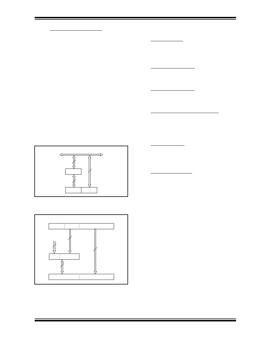
©
1996 Microchip Technology Inc.
DS30412C-page 41
PIC17C4X
6.7
Program Counter Module
The Program Counter (PC) is a 16-bit register. PCL, the
low byte of the PC, is mapped in the data memory. PCL
is readable and writable just as is any other register.
PCH is the high byte of the PC and is not directly
addressable. Since PCH is not mapped in data or pro-
gram memory, an 8-bit register PCLATH (PC high latch)
is used as a holding latch for the high byte of the PC.
PCLATH is mapped into data memory. The user can
read or write PCH through PCLATH.
The 16-bit wide PC is incremented after each instruc-
tion fetch during Q1 unless:
∑ Modified by
GOTO
,
CALL
,
LCALL
,
RETURN
,
RETLW
,
or
RETFIE
instruction
∑ Modified by an interrupt response
∑ Due to destination write to PCL by an instruction
"Skips" are equivalent to a forced NOP cycle at the
skipped address.
Figure 6-11 and Figure 6-12 show the operation of the
program counter for various situations.
FIGURE 6-11: PROGRAM COUNTER
OPERATION
FIGURE 6-12: PROGRAM COUNTER USING
THE CALL AND GOTO
INSTRUCTIONS
Internal data bus <8>
PCLATH
8
8
8
PCH
PCL
8
15
0
7
5 4
0
12
8 7
0
8 7
Last write
to PCLATH
PCLATH
Opcode
5
3
8
PCH
PCL
13
15
Using Figure 6-11, the operations of the PC and
PCLATH for different instructions are as follows:
a)
LCALL
instructions:
An 8-bit destination address is provided in the
instruction (opcode). PCLATH is unchanged.
PCLATH
PCH
Opcode<7:0>
PCL
b)
Read instructions on PCL:
Any instruction that reads PCL.
PCL
data bus
ALU or destination
PCH
PCLATH
c)
Write instructions on PCL:
Any instruction that writes to PCL.
8-bit data
data bus
PCL
PCLATH
PCH
d)
Read-Modify-Write instructions on PCL:
Any instruction that does a read-write-modify
operation on PCL, such as
ADDWF PCL
.
Read:
PCL
data bus
ALU
Write:
8-bit result
data bus
PCL
PCLATH
PCH
e)
RETURN
instruction:
PCH
PCLATH
Stack<MRU>
PC<15:0>
Using Figure
6-12, the operation of the PC and
PCLATH for
GOTO
and
CALL
instructions is a follows:
CALL
,
GOTO
instructions:
A 13-bit destination address is provided in the
instruction (opcode).
Opcode<12:0>
PC <12:0>
PC<15:13>
PCLATH<7:5>
Opcode<12:8>
PCLATH <4:0>
The read-modify-write only affects the PCL with the
result. PCH is loaded with the value in the PCLATH.
For example,
ADDWF PCL
will result in a jump within the
current page. If PC = 03F0h, WREG = 30h and
PCLATH = 03h before instruction, PC = 0320h after the
instruction. To accomplish a true 16-bit computed jump,
the user needs to compute the 16-bit destination
address, write the high byte to PCLATH and then write
the low value to PCL.
The following PC related operations do not change
PCLATH:
a)
LCALL
,
RETLW
, and
RETFIE
instructions.
b)
Interrupt vector is forced onto the PC.
c)
Read-modify-write instructions on PCL (e.g.
BSF
PCL
).

PIC17C4X
DS30412C-page 42
©
1996 Microchip Technology Inc.
6.8
Bank Select Register (BSR)
The BSR is used to switch between banks in the data
memory area (Figure
6-13). In the PIC17C42,
PIC17CR42, and PIC17C42A only the lower nibble is
implemented. While in the PIC17C43, PIC17CR43,
and PIC17C44 devices, the entire byte is implemented.
The lower nibble is used to select the peripheral regis-
ter bank. The upper nibble is used to select the general
purpose memory bank.
All the Special Function Registers (SFRs) are mapped
into the data memory space. In order to accommodate
the large number of registers, a banking scheme has
been used. A segment of the SFRs, from address 10h
to address 17h, is banked. The lower nibble of the bank
select register (BSR) selects the currently active
"peripheral bank." Effort has been made to group the
peripheral registers of related functionality in one bank.
However, it will still be necessary to switch from bank
to bank in order to address all peripherals related to a
single task. To assist this, a
MOVLB bank
instruction is
in the instruction set.
For the PIC17C43, PIC17CR43, and PIC17C44
devices, the need for a large general purpose memory
space dictated a general purpose RAM banking
scheme. The upper nibble of the BSR selects the cur-
rently active general purpose RAM bank. To assist this,
a
MOVLR bank
instruction has been provided in the
instruction set.
If the currently selected bank is not implemented (such
as Bank 13), any read will read all '0's. Any write is com-
pleted to the bit bucket and the ALU status bits will be
set/cleared as appropriate.
Note:
Registers in Bank 15 in the Special Func-
tion Register area, are reserved for
Microchip use. Reading of registers in this
bank may cause random values to be read.
FIGURE 6-13: BSR OPERATION (PIC17C43/R43/44)
7
4 3
0
10h
17h
BSR
0
1
2
3
4
15
∑ ∑ ∑
20h
FFh
∑ ∑ ∑
∑ ∑ ∑
(1)
(2)
Bank 15
Bank 4
Bank 3
Bank 2
Bank 1
Bank 0
0
1
2
Bank 2
Bank 1
Bank 0
15
Bank 15
SFR
Banks
GPR
Banks
Address
Range
Note 1:
Only Banks 0 through Bank 3 are implemented. Selection of an unimplemented bank is not recommended.
Bank 15 is reserved for Microchip use, reading of registers in this bank may cause random values to be read.
2:
Only Banks 0 and Bank 1 are implemented. Selection of an unimplemented bank is not recommended.

©
1996 Microchip Technology Inc.
DS30412C-page 43
PIC17C4X
7.0
TABLE READS AND TABLE
WRITES
The PIC17C4X has four instructions that allow the pro-
cessor to move data from the data memory space to
the program memory space, and vice versa. Since the
program memory space is 16-bits wide and the data
memory space is 8-bits wide, two operations are
required to move 16-bit values to/from the data mem-
ory.
The
TLWT t,f
and
TABLWT t,i,f
instructions are
used to write data from the data memory space to the
program memory space. The
TLRD t,f
and
TABLRD
t,i,f
instructions are used to write data from the pro-
gram memory space to the data memory space.
The program memory can be internal or external. For
the program memory access to be external, the device
needs to be operating in extended microcontroller or
microprocessor mode.
Figure 7-1 through Figure 7-4 show the operation of
these four instructions.
FIGURE 7-1:
TLWT INSTRUCTION
OPERATION
TABLE POINTER
TABLE LATCH (16-bit)
PROGRAM MEMORY
DATA
MEMORY
TBLPTRH
TBLPTRL
TABLATH
TABLATL
f
TLWT 1,f
TLWT 0,f
1
Note 1: 8-bit value, from register 'f', loaded into the
high or low byte in TABLAT (16-bit).
FIGURE 7-2:
TABLWT INSTRUCTION
OPERATION
TABLE POINTER
TABLE LATCH (16-bit)
PROGRAM MEMORY
DATA
MEMORY
TBLPTRH
TBLPTRL
TABLATH
TABLATL
f
TABLWT 1,i,f
TABLWT 0,i,f
1
Prog-Mem
(TBLPTR)
2
Note 1: 8-bit value, from register 'f', loaded into
the high or low byte in TABLAT (16-bit).
2: 16-bit TABLAT value written to address
Program Memory (TBLPTR).
3: If "i" = 1, then TBLPTR = TBLPTR + 1,
If "i" = 0, then TBLPTR is unchanged.
3
3
This document was created with FrameMaker 4 0 4

PIC17C4X
DS30412C-page 44
©
1996 Microchip Technology Inc.
FIGURE 7-3:
TLRD INSTRUCTION
OPERATION
TABLE POINTER
TABLE LATCH (16-bit)
PROGRAM MEMORY
DATA
MEMORY
TBLPTRH
TBLPTRL
TABLATH
TABLATL
f
TLRD 1,f
TLRD 0,f
1
Note 1: 8-bit value, from TABLAT (16-bit) high or
low byte, loaded into register 'f'.
FIGURE 7-4:
TABLRD INSTRUCTION
OPERATION
TABLE POINTER
TABLE LATCH (16-bit)
PROGRAM MEMORY
DATA
MEMORY
TBLPTRH
TBLPTRL
TABLATH
TABLATL
f
TABLRD 1,i,f
TABLRD 0,i,f
1
Prog-Mem
(TBLPTR)
2
Note 1: 8-bit value, from TABLAT (16-bit) high or
low byte, loaded into register 'f'.
2: 16-bit value at Program Memory (TBLPTR)
loaded into TABLAT register.
3: If "i" = 1, then TBLPTR = TBLPTR + 1,
If "i" = 0, then TBLPTR is unchanged.
3
3

©
1996 Microchip Technology Inc.
DS30412C-page 45
PIC17C4X
7.1
Table Writes to Internal Memory
A table write operation to internal memory causes a
long write operation. The long write is necessary for
programming the internal EPROM. Instruction execu-
tion is halted while in a long write cycle. The long write
will be terminated by any enabled interrupt. To ensure
that the EPROM location has been well programmed,
a minimum programming time is required (see specifi-
cation #D114 ). Having only one interrupt enabled to
terminate the long write ensures that no unintentional
interrupts will prematurely terminate the long write.
The sequence of events for programming an internal
program memory location should be:
1.
Disable all interrupt sources, except the source
to terminate EPROM program write.
2.
Raise MCLR/V
PP
pin to the programming volt-
age.
3.
Clear the WDT.
4.
Do the table write. The interrupt will terminate
the long write.
5.
Verify the memory location (table read).
Note:
Programming requirements must be met.
See timing specification in electrical spec-
ifications for the desired device. Violating
these specifications (including tempera-
ture) may result in EPROM locations that
are not fully programmed and may lose
their state over time.
7.1.1
TERMINATING LONG WRITES
An interrupt source or reset are the only events that
terminate a long write operation. Terminating the long
write from an interrupt source requires that the inter-
rupt enable and flag bits are set. The GLINTD bit only
enables the vectoring to the interrupt address.
If the T0CKI, RA0/INT, or TMR0 interrupt source is
used to terminate the long write; the interrupt flag, of
the highest priority enabled interrupt, will terminate the
long write and automatically be cleared.
If a peripheral interrupt source is used to terminate the
long write, the interrupt enable and flag bits must be
set. The interrupt flag will not be automatically cleared
upon the vectoring to the interrupt vector address.
If the GLINTD bit is cleared prior to the long write,
when the long write is terminated, the program will
branch to the interrupt vector.
If the GLINTD bit is set prior to the long write, when
the long write is terminated, the program will not vector
to the interrupt address.
Note 1:
If an interrupt is pending, the TABLWT is
aborted (an NOP is executed). The
highest priority pending interrupt, from
the T0CKI, RA0/INT, or TMR0 sources
that is enabled, has its flag cleared.
Note 2:
If the interrupt is not being used for the
program write timing, the interrupt
should be disabled. This will ensure that
the interrupt is not lost, nor will it termi-
nate the long write prematurely.
TABLE 7-1:
INTERRUPT - TABLE WRITE INTERACTION
Interrupt
Source
GLINTD
Enable
Bit
Flag
Bit
Action
RA0/INT, TMR0,
T0CKI
0
0
1
1
1
1
0
1
1
0
x
1
Terminate long table write (to internal program
memory), branch to interrupt vector (branch clears
flag bit).
None
None
Terminate table write, do not branch to interrupt
vector (flag is automatically cleared).
Peripheral
0
0
1
1
1
1
0
1
1
0
x
1
Terminate table write, branch to interrupt vector.
None
None
Terminate table write, do not branch to interrupt
vector (flag is set).

PIC17C4X
DS30412C-page 46
©
1996 Microchip Technology Inc.
7.2
Table Writes to External Memory
Table writes to external memory are always two-cycle
instructions. The second cycle writes the data to the
external memory location. The sequence of events for
an external memory write are the same for an internal
write.
Note:
If an interrupt is pending or occurs during
the
TABLWT
, the two cycle table write
completes. The RA0/INT, TMR0, or T0CKI
interrupt flag is automatically cleared or
the pending peripheral interrupt is
acknowledged.
7.2.2
TABLE WRITE CODE
The "i" operand of the
TABLWT
instruction can specify
that the value in the 16-bit TBLPTR register is auto-
matically incremented for the next write. In
Example 7-1, the TBLPTR register is not automatically
incremented.
EXAMPLE 7-1:
TABLE WRITE
CLRWDT ; Clear WDT
MOVLW HIGH (TBL_ADDR) ; Load the Table
MOVWF TBLPTRH ; address
MOVLW LOW (TBL_ADDR) ;
MOVWF TBLPTRL ;
MOVLW HIGH (DATA) ; Load HI byte
TLWT 1, WREG ; in TABLATCH
MOVLW LOW (DATA) ; Load LO byte
TABLWT 0,0,WREG ; in TABLATCH
; and write to
; program memory
; (Ext. SRAM)
FIGURE 7-5:
TABLWT WRITE TIMING (EXTERNAL MEMORY)
Q1 Q2 Q3 Q4
Q1 Q2 Q3 Q4
Q1 Q2 Q3 Q4
Q1 Q2 Q3 Q4
AD15:AD0
Instruction
fetched
Instruction
executed
ALE
OE
WR
TABLWT
INST (PC+1)
INST (PC-1)
TABLWT cycle1
TABLWT cycle2
INST (PC+2)
Data write cycle
'1'
PC
PC+1
TBL
PC+2
Data out
INST (PC+1)
Note:
If external write GLINTD = '1', Enable bit = '1', '1'
Flag bit, Do table write. The highest pending interrupt is cleared.

©
1996 Microchip Technology Inc.
DS30412C-page 47
PIC17C4X
FIGURE 7-6:
CONSECUTIVE TABLWT WRITE TIMING (EXTERNAL MEMORY)
Q1 Q2 Q3 Q4 Q1 Q2 Q3 Q4 Q1 Q2 Q3 Q4 Q1 Q2 Q3 Q4 Q1 Q2 Q3 Q4 Q1 Q2 Q3 Q4
AD15:AD0
Instruction
fetched
Instruction
executed
ALE
OE
WR
PC
TABLWT1
TABLWT2
INST (PC+2)
INST (PC-1)
TABLWT1 cycle1 TABLWT1 cycle2 TABLWT2 cycle1 TABLWT2 cycle2
Data write cycle
Data write cycle
INST (PC+3)
PC+1
TBL1
PC+2
TBL2
PC+3
Data out 1
Data out 2
INST (PC+2)
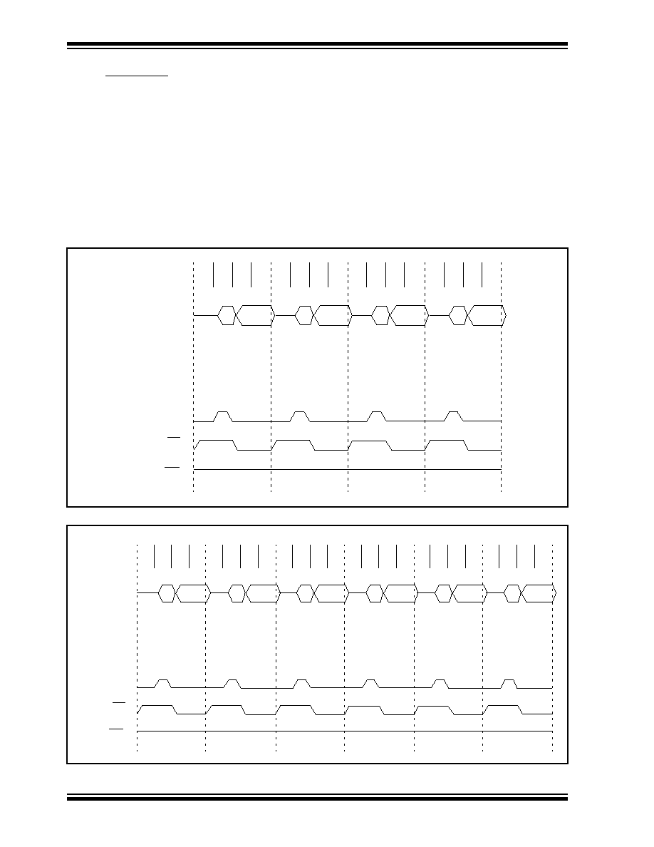
PIC17C4X
DS30412C-page 48
©
1996 Microchip Technology Inc.
7.3
Table Reads
The table read allows the program memory to be read.
This allows constant data to be stored in the program
memory space, and retrieved into data memory when
needed. Example 7-2 reads the 16-bit value at pro-
gram memory address TBLPTR. After the dummy byte
has been read from the TABLATH, the TABLATH is
loaded with the 16-bit data from program memory
address TBLPTR + 1. The first read loads the data into
the latch, and can be considered a dummy read
(unknown data loaded into 'f'). INDF0 should be con-
figured for either auto-increment or auto-decrement.
EXAMPLE 7-2:
TABLE READ
MOVLW HIGH (TBL_ADDR) ; Load the Table
MOVWF TBLPTRH ; address
MOVLW LOW (TBL_ADDR) ;
MOVWF TBLPTRL ;
TABLRD 0,0,DUMMY ; Dummy read,
; Updates TABLATCH
TLRD 1, INDF0 ; Read HI byte
; of TABLATCH
TABLRD 0,1,INDF0 ; Read LO byte
; of TABLATCH and
; Update TABLATCH
FIGURE 7-7:
TABLRD TIMING
FIGURE 7-8:
TABLRD TIMING (CONSECUTIVE TABLRD INSTRUCTIONS)
Q1 Q2 Q3 Q4 Q1 Q2 Q3 Q4 Q1 Q2 Q3 Q4 Q1 Q2 Q3 Q4
AD15:AD0
Instruction
fetched
Instruction
executed
ALE
OE
WR
TABLRD
INST (PC+1)
INST (PC+2)
INST (PC-1)
TABLRD cycle1
TABLRD cycle2
INST (PC+1)
Data read cycle
PC
PC+1
TBL
Data in
PC+2
'1'
Q1 Q2 Q3 Q4 Q1 Q2 Q3 Q4 Q1 Q2 Q3 Q4 Q1 Q2 Q3 Q4 Q1 Q2 Q3 Q4 Q1 Q2 Q3 Q4
AD15:AD0
Instruction
fetched
Instruction
executed
TABLRD1
TABLRD2
INST (PC+2)
INST (PC+3)
INST (PC+2)
ALE
OE
WR
INST (PC-1)
TABLRD1 cycle1 TABLRD1 cycle2 TABLRD2 cycle1 TABLRD2 cycle2
Data read cycle
Data read cycle
'1'
PC
PC+1
PC+2
PC+3
TBL1 Data in 1
TBL2
Data in 2
©
1996 Microchip Technology Inc.
DS30412C-page 49
PIC17C4X
8.0
HARDWARE MULTIPLIER
All PIC17C4X devices except the PIC17C42, have an
8 x 8 hardware multiplier included in the ALU of the
device. By making the multiply a hardware operation, it
completes in a single instruction cycle. This is an
unsigned multiply that gives a 16-bit result. The result
is stored into the 16-bit PRODuct register
(PRODH:PRODL). The multiplier does not affect any
flags in the ALUSTA register.
Making the 8 x 8 multiplier execute in a single cycle
gives the following advantages:
∑ Higher computational throughput
∑ Reduces code size requirements for multiply
algorithms
The performance increase allows the device to be used
in applications previously reserved for Digital Signal
Processors.
Table 8-1 shows a performance comparison between
the PIC17C42 and all other PIC17CXX devices, which
have the single cycle hardware multiply.
Example 8-1 shows the sequence to do an 8 x 8
unsigned multiply. Only one instruction is required
when one argument of the multiply is already loaded in
the WREG register.
Example 8-2 shows the sequence to do an 8 x 8 signed
multiply. To account for the sign bits of the arguments,
each argument's most significant bit (MSb) is tested
and the appropriate subtractions are done.
EXAMPLE 8-1:
8 x 8 MULTIPLY ROUTINE
MOVFP ARG1, WREG
MULWF ARG2 ; ARG1 * ARG2 ->
; PRODH:PRODL
EXAMPLE 8-2:
8 x 8 SIGNED MULTIPLY
ROUTINE
MOVFP ARG1, WREG
MULWF ARG2 ; ARG1 * ARG2 ->
; PRODH:PRODL
BTFSC ARG2, SB ; Test Sign Bit
SUBWF PRODH, F ; PRODH = PRODH
; - ARG1
MOVFP ARG2, WREG
BTFSC ARG1, SB ; Test Sign Bit
SUBWF PRODH, F ; PRODH = PRODH
; - ARG2
TABLE 8-1:
PERFORMANCE COMPARISON
Routine
Device
Program Memory
(Words)
Cycles (Max)
Time
@ 25 MHz
@ 33 MHz
8 x 8 unsigned
PIC17C42
13
69
11.04
µ
s
N/A
All other PIC17CXX devices
1
1
160 ns
121 ns
8 x 8 signed
PIC17C42
--
--
--
N/A
All other PIC17CXX devices
6
6
960 ns
727 ns
16 x 16 unsigned
PIC17C42
21
242
38.72
µ
s
N/A
All other PIC17CXX devices
24
24
3.84
µ
s
2.91
µ
s
16 x 16 signed
PIC17C42
52
254
40.64
µ
s
N/A
All other PIC17CXX devices
36
36
5.76
µ
s
4.36
µ
s
This document was created with FrameMaker 4 0 4

PIC17C4X
DS30412C-page 50
©
1996 Microchip Technology Inc.
Example 8-3 shows the sequence to do a 16 x 16
unsigned multiply. Equation 8-1 shows the algorithm
that is used. The 32-bit result is stored in 4 registers
RES3:RES0.
EQUATION 8-1:
16 x 16 UNSIGNED
MULTIPLICATION
ALGORITHM
RES3:RES0
=
ARG1H:ARG1L * ARG2H:ARG2L
=
(ARG1H * ARG2H * 2
16
) +
(ARG1H * ARG2L * 2
8
)
+
(ARG1L * ARG2H * 2
8
)
+
(ARG1L * ARG2L)
EXAMPLE 8-3:
16 x 16 MULTIPLY ROUTINE
MOVFP ARG1L, WREG
MULWF ARG2L ; ARG1L * ARG2L ->
; PRODH:PRODL
MOVPF PRODH, RES1 ;
MOVPF PRODL, RES0 ;
;
MOVFP ARG1H, WREG
MULWF ARG2H ; ARG1H * ARG2H ->
; PRODH:PRODL
MOVPF PRODH, RES3 ;
MOVPF PRODL, RES2 ;
;
MOVFP ARG1L, WREG
MULWF ARG2H ; ARG1L * ARG2H ->
; PRODH:PRODL
MOVFP PRODL, WREG ;
ADDWF RES1, F ; Add cross
MOVFP PRODH, WREG ; products
ADDWFC RES2, F ;
CLRF WREG, F ;
ADDWFC RES3, F ;
;
MOVFP ARG1H, WREG ;
MULWF ARG2L ; ARG1H * ARG2L ->
; PRODH:PRODL
MOVFP PRODL, WREG ;
ADDWF RES1, F ; Add cross
MOVFP PRODH, WREG ; products
ADDWFC RES2, F ;
CLRF WREG, F ;
ADDWFC RES3, F ;

©
1996 Microchip Technology Inc.
DS30412C-page 51
PIC17C4X
Example 8-4 shows the sequence to do an 16 x 16
signed multiply. Equation 8-2 shows the algorithm that
used. The 32-bit result is stored in four registers
RES3:RES0. To account for the sign bits of the argu-
ments, each argument pairs most significant bit (MSb)
is tested and the appropriate subtractions are done.
EQUATION 8-2:
16 x 16 SIGNED
MULTIPLICATION
ALGORITHM
RES3:RES0
= ARG1H:ARG1L * ARG2H:ARG2L
= (ARG1H * ARG2H * 2
16
)
+
(ARG1H * ARG2L * 2
8
)
+
(ARG1L * ARG2H * 2
8
)
+
(ARG1L * ARG2L)
+
(-1 * ARG2H<7> * ARG1H:ARG1L * 2
16
) +
(-1 * ARG1H<7> * ARG2H:ARG2L * 2
16
)
EXAMPLE 8-4:
16 x 16 SIGNED MULTIPLY
ROUTINE
MOVFP ARG1L, WREG
MULWF ARG2L ; ARG1L * ARG2L ->
; PRODH:PRODL
MOVPF PRODH, RES1 ;
MOVPF PRODL, RES0 ;
;
MOVFP ARG1H, WREG
MULWF ARG2H ; ARG1H * ARG2H ->
; PRODH:PRODL
MOVPF PRODH, RES3 ;
MOVPF PRODL, RES2 ;
;
MOVFP ARG1L, WREG
MULWF ARG2H ; ARG1L * ARG2H ->
; PRODH:PRODL
MOVFP PRODL, WREG ;
ADDWF RES1, F ; Add cross
MOVFP PRODH, WREG ; products
ADDWFC RES2, F ;
CLRF WREG, F ;
ADDWFC RES3, F ;
;
MOVFP ARG1H, WREG ;
MULWF ARG2L ; ARG1H * ARG2L ->
; PRODH:PRODL
MOVFP PRODL, WREG ;
ADDWF RES1, F ; Add cross
MOVFP PRODH, WREG ; products
ADDWFC RES2, F ;
CLRF WREG, F ;
ADDWFC RES3, F ;
;
BTFSS ARG2H, 7 ; ARG2H:ARG2L neg?
GOTO SIGN_ARG1 ; no, check ARG1
MOVFP ARG1L, WREG ;
SUBWF RES2 ;
MOVFP ARG1H, WREG ;
SUBWFB RES3
;
SIGN_ARG1
BTFSS ARG1H, 7 ; ARG1H:ARG1L neg?
GOTO CONT_CODE ; no, done
MOVFP ARG2L, WREG ;
SUBWF RES2 ;
MOVFP ARG2H, WREG ;
SUBWFB RES3
;
CONT_CODE
:

PIC17C4X
DS30412C-page 52
©
1996 Microchip Technology Inc.
NOTES:
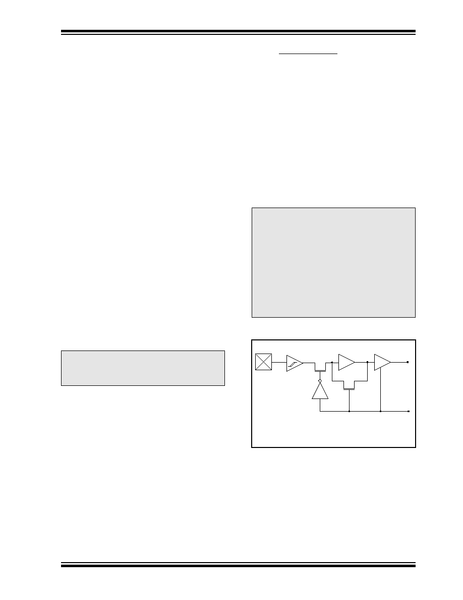
©
1996 Microchip Technology Inc.
DS30412C-page 53
PIC17C4X
9.0
I/O PORTS
The PIC17C4X devices have five I/O ports, PORTA
through PORTE. PORTB through PORTE have a corre-
sponding Data Direction Register (DDR), which is used
to configure the port pins as inputs or outputs. These
five ports are made up of 33 I/O pins. Some of these
ports pins are multiplexed with alternate functions.
PORTC, PORTD, and PORTE are multiplexed with the
system bus. These pins are configured as the system
bus when the device's configuration bits are selected to
Microprocessor or Extended Microcontroller modes. In
the two other microcontroller modes, these pins are
general purpose I/O.
PORTA and PORTB are multiplexed with the peripheral
features of the device. These peripheral features are:
∑ Timer modules
∑ Capture module
∑ PWM module
∑ USART/SCI module
∑ External Interrupt pin
When some of these peripheral modules are turned on,
the port pin will automatically configure to the alternate
function. The modules that do this are:
∑ PWM module
∑ USART/SCI module
When a pin is automatically configured as an output by
a peripheral module, the pins data direction (DDR) bit
is unknown. After disabling the peripheral module, the
user should re-initialize the DDR bit to the desired con-
figuration.
The other peripheral modules (which require an input)
must have their data direction bit configured appropri-
ately.
Note:
A pin that is a peripheral input, can be con-
figured as an output (DDRx<y> is cleared).
The peripheral events will be determined
by the action output on the port pin.
9.1
PORTA Register
PORTA is a 6-bit wide latch. PORTA does not have a
corresponding Data Direction Register (DDR).
Reading PORTA reads the status of the pins.
The RA1 pin is multiplexed with TMR0 clock input, and
RA4 and RA5 are multiplexed with the USART func-
tions. The control of RA4 and RA5 as outputs is auto-
matically configured by the USART module.
9.1.1
USING RA2, RA3 AS OUTPUTS
The RA2 and RA3 pins are open drain outputs. To use
the RA2 or the RA3 pin(s) as output(s), simply write to
the PORTA register the desired value. A '0' will cause
the pin to drive low, while a '1' will cause the pin to float
(hi-impedance). An external pull-up resistor should be
used to pull the pin high. Writes to PORTA will not affect
the other pins.
FIGURE 9-1:
RA0 AND RA1 BLOCK
DIAGRAM
Note:
When using the RA2 or RA3 pin(s) as out-
put(s), read-modify-write instructions (such
as
BCF
,
BSF
,
BTG
) on PORTA are not rec-
ommended.
Such operations read the port pins, do the
desired operation, and then write this value
to the data latch. This may inadvertently
cause the RA2 or RA3 pins to switch from
input to output (or vice-versa).
It is recommended to use a shadow regis-
ter for PORTA. Do the bit operations on this
shadow register and then move it to
PORTA.
Note: I/O pins have protection diodes to V
DD
and V
SS
.
DATA BUS
RD_PORTA
(Q2)
This document was created with FrameMaker 4 0 4
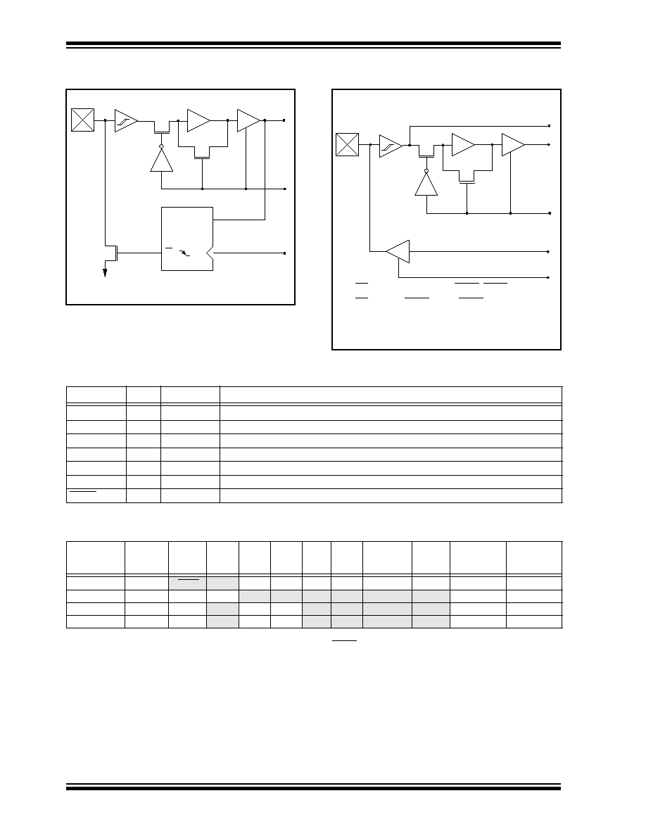
PIC17C4X
DS30412C-page 54
©
1996 Microchip Technology Inc.
FIGURE 9-2:
RA2 AND RA3 BLOCK
DIAGRAM
Note: I/O pins have protection diodes to V
SS
.
Data Bus
WR_PORTA
(Q4)
Q
D
Q
CK
RD_PORTA
(Q2)
FIGURE 9-3:
RA4 AND RA5 BLOCK
DIAGRAM
Note: I/O pins have protection diodes to V
DD
and V
SS
.
Data Bus
RD_PORTA
(Q2)
Serial port output signals
Serial port input signal
OE = SPEN,SYNC,TXEN, CREN, SREN for RA4
OE = SPEN (SYNC+SYNC,CSRC) for RA5
TABLE 9-1:
PORTA FUNCTIONS
TABLE 9-2:
REGISTERS/BITS ASSOCIATED WITH PORTA
Name
Bit0
Buffer Type
Function
RA0/INT
bit0
ST
Input or external interrupt input.
RA1/T0CKI
bit1
ST
Input or clock input to the TMR0 timer/counter, and/or an external interrupt input.
RA2
bit2
ST
Input/Output. Output is open drain type.
RA3
bit3
ST
Input/Output. Output is open drain type.
RA4/RX/DT
bit4
ST
Input or USART Asynchronous Receive or USART Synchronous Data.
RA5/TX/CK
bit5
ST
Input or USART Asynchronous Transmit or USART Synchronous Clock.
RBPU
bit7
--
Control bit for PORTB weak pull-ups.
Legend: ST = Schmitt Trigger input.
Address
Name
Bit 7
Bit 6
Bit 5
Bit 4
Bit 3
Bit 2
Bit 1
Bit 0
Value on
Power-on
Reset
Value on all
other resets
(Note1)
10h, Bank 0
PORTA
RBPU
--
RA5
RA4
RA3
RA2
RA1/T0CKI
RA0/INT
0-xx xxxx
0-uu uuuu
05h, Unbanked
T0STA
INTEDG
T0SE
T0CS
PS3
PS2
PS1
PS0
--
0000 000-
0000 000-
13h, Bank 0
RCSTA
SPEN
RC9
SREN
CREN
--
FERR
OERR
RC9D
0000 -00x
0000 -00u
15h, Bank 0
TXSTA
CSRC
TX9
TXEN
SYNC
--
--
TRMT
TX9D
0000 --1x
0000 --1u
Legend:
x
= unknown,
u
= unchanged,
-
= unimplemented reads as '0'. Shaded cells are not used by PORTA.
Note 1:
Other (non power-up) resets include: external reset through MCLR and the Watchdog Timer Reset.
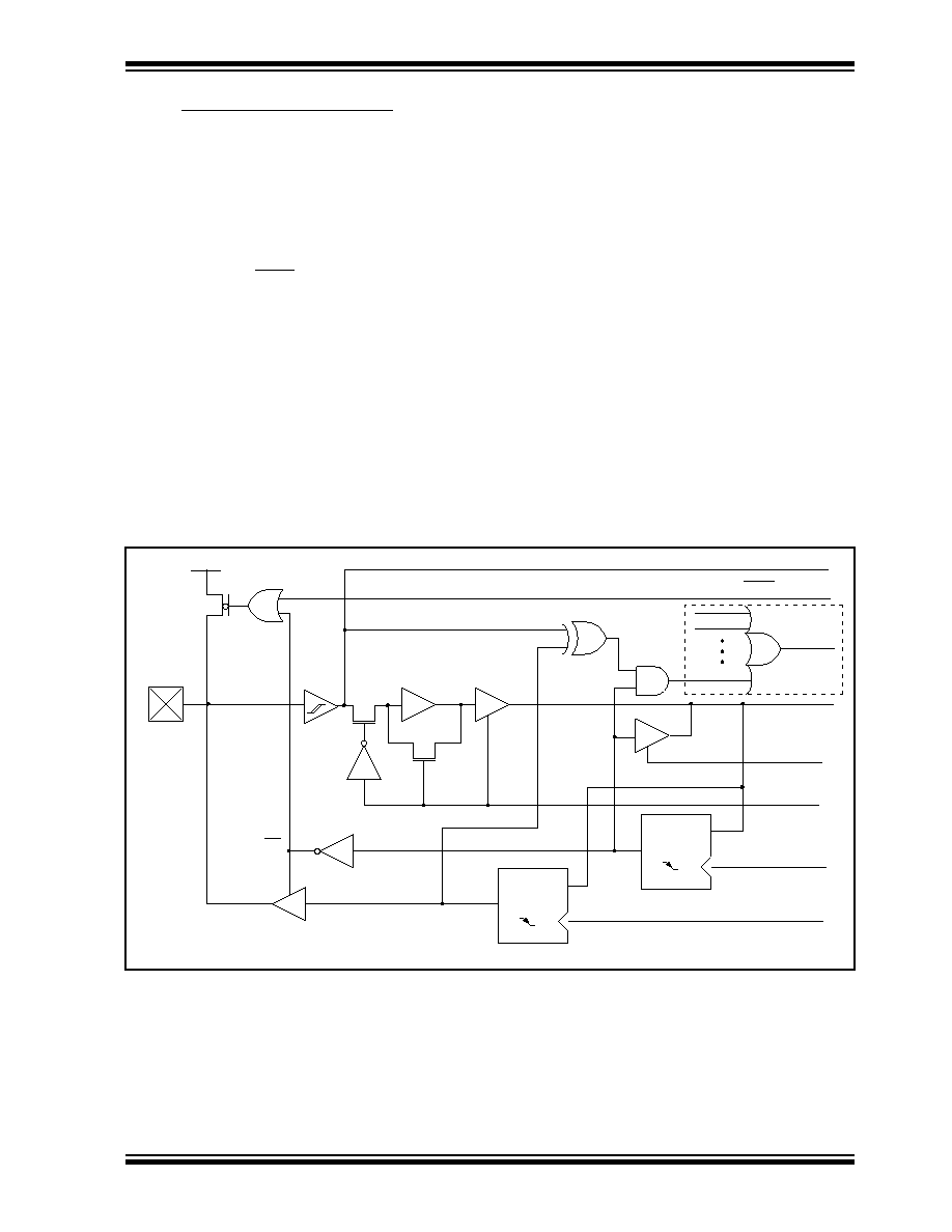
©
1996 Microchip Technology Inc.
DS30412C-page 55
PIC17C4X
9.2
PORTB and DDRB Registers
PORTB is an 8-bit wide bi-directional port. The corre-
sponding data direction register is DDRB. A '1' in DDRB
configures the corresponding port pin as an input. A '0'
in the DDRB register configures the corresponding port
pin as an output. Reading PORTB reads the status of
the pins, whereas writing to it will write to the port latch.
Each of the PORTB pins has a weak internal pull-up. A
single control bit can turn on all the pull-ups. This is
done by clearing the RBPU (PORTA<7>) bit. The weak
pull-up is automatically turned off when the port pin is
configured as an output. The pull-ups are enabled on
any reset.
PORTB also has an interrupt on change feature. Only
pins configured as inputs can cause this interrupt to
occur (i.e. any RB7:RB0 pin configured as an output is
excluded from the interrupt on change comparison).
The input pins (of RB7:RB0) are compared with the
value in the PORTB data latch. The "mismatch" outputs
of RB7:RB0 are OR'ed together to generate the
PORTB Interrupt Flag RBIF (PIR<7>).
This interrupt can wake the device from SLEEP. The
user, in the interrupt service routine, can clear the inter-
rupt by:
a)
Read-Write PORTB (such as;
MOVPF PORTB,
PORTB
). This will end mismatch condition.
b)
Then, clear the RBIF bit.
A mismatch condition will continue to set the RBIF bit.
Reading then writing PORTB will end the mismatch
condition, and allow the RBIF bit to be cleared.
This interrupt on mismatch feature, together with soft-
ware configurable pull-ups on this port, allows easy
interface to a key pad and make it possible for wake-up
on key-depression. For an example, refer to AN552 in
the
Embedded Control Handbook
.
The interrupt on change feature is recommended for
wake-up on operations where PORTB is only used for
the interrupt on change feature and key depression
operation.
FIGURE 9-4:
BLOCK DIAGRAM OF RB<7:4> AND RB<1:0> PORT PINS
Note: I/O pins have protection diodes to V
DD
and V
SS
.
Data Bus
Q
D
CK
Q
D
CK
Weak
Pull-Up
Port
Input Latch
Port
Data
OE
WR_PORTB (Q4)
WR_DDRB (Q4)
RD_PORTB (Q2)
RD_DDRB (Q2)
RBIF
RBPU
Match Signal
from other
port pins
(PORTA<7>)
Peripheral Data in

PIC17C4X
DS30412C-page 56
©
1996 Microchip Technology Inc.
FIGURE 9-5:
BLOCK DIAGRAM OF RB3 AND RB2 PORT PINS
Note: I/O pins have protection diodes to V
DD
and Vss.
Data Bus
Q
D
CK
Q
D
CK
R
Weak
Pull-Up
Port
Input Latch
Port
Data
OE
PWM_select
PWM_output
WR_PORTB (Q4)
WR_DDRB (Q4)
RD_PORTB (Q2)
RD_DDRB (Q2)
RBIF
RBPU
Match Signal
from other
port pins
(PORTA<7>)
Peripheral Data in

©
1996 Microchip Technology Inc.
DS30412C-page 57
PIC17C4X
Example 9-1 shows the instruction sequence to initial-
ize PORTB. The Bank Select Register (BSR) must be
selected to Bank 0 for the port to be initialized.
EXAMPLE 9-1:
INITIALIZING PORTB
MOVLB 0
; Select Bank 0
CLRF
PORTB
; Initialize PORTB by clearing
; output data latches
MOVLW 0xCF
; Value used to initialize
; data direction
MOVWF DDRB
; Set RB<3:0> as inputs
; RB<5:4> as outputs
; RB<7:6> as inputs
TABLE 9-3:
PORTB FUNCTIONS
TABLE 9-4:
REGISTERS/BITS ASSOCIATED WITH PORTB
Name
Bit
Buffer Type
Function
RB0/CAP1
bit0
ST
Input/Output or the RB0/CAP1 input pin. Software programmable weak pull-
up and interrupt on change features.
RB1/CAP2
bit1
ST
Input/Output or the RB1/CAP2 input pin. Software programmable weak pull-
up and interrupt on change features.
RB2/PWM1
bit2
ST
Input/Output or the RB2/PWM1 output pin. Software programmable weak
pull-up and interrupt on change features.
RB3/PWM2
bit3
ST
Input/Output or the RB3/PWM2 output pin. Software programmable weak
pull-up and interrupt on change features.
RB4/TCLK12
bit4
ST
Input/Output or the external clock input to Timer1 and Timer2. Software pro-
grammable weak pull-up and interrupt on change features.
RB5/TCLK3
bit5
ST
Input/Output or the external clock input to Timer3. Software programmable
weak pull-up and interrupt on change features.
RB6
bit6
ST
Input/Output pin. Software programmable weak pull-up and interrupt on
change features.
RB7
bit7
ST
Input/Output pin. Software programmable weak pull-up and interrupt on
change features.
Legend: ST = Schmitt Trigger input.
Address
Name
Bit 7
Bit 6
Bit 5
Bit 4
Bit 3
Bit 2
Bit 1
Bit 0
Value on
Power-on
Reset
Value on all
other
resets
(Note1)
12h, Bank 0
PORTB
PORTB data latch
xxxx xxxx
uuuu uuuu
11h, Bank 0
DDRB
Data direction register for PORTB
1111 1111
1111 1111
10h, Bank 0
PORTA
RBPU
--
RA5
RA4
RA3
RA2
RA1/T0CKI
RA0/INT
0-xx xxxx
0-uu uuuu
06h, Unbanked
CPUSTA
--
--
STKAV
GLINTD
TO
PD
--
--
--11 11--
--11 qq--
07h, Unbanked
INTSTA
PEIF
T0CKIF
T0IF
INTF
PEIE
T0CKIE
T0IE
INTE
0000 0000
0000 0000
16h, Bank 1
PIR
RBIF
TMR3IF
TMR2IF
TMR1IF
CA2IF
CA1IF
TXIF
RCIF
0000 0010
0000 0010
17h, Bank 1
PIE
RBIE
TMR3IE
TMR2IE
TMR1IE
CA2IE
CA1IE
TXIE
RCIE
0000 0000
0000 0000
16h, Bank 3
TCON1
CA2ED1
CA2ED0
CA1ED1
CA1ED0
T16
TMR3CS
TMR2CS
TMR1CS
0000 0000
0000 0000
17h, Bank 3
TCON2
CA2OVF CA1OVF
PWM2ON
PWM1ON
CA1/PR3
TMR3ON
TMR2ON
TMR1ON
0000 0000
0000 0000
Legend:
x
= unknown,
u
= unchanged,
-
= unimplemented read as '0', q = Value depends on condition.
Shaded cells are not used by PORTB.
Note 1:
Other (non power-up) resets include: external reset through MCLR and the Watchdog Timer Reset.

PIC17C4X
DS30412C-page 58
©
1996 Microchip Technology Inc.
9.3
PORTC and DDRC Registers
PORTC is an 8-bit bi-directional port. The correspond-
ing data direction register is DDRC. A '1' in DDRC con-
figures the corresponding port pin as an input. A '0' in
the DDRC register configures the corresponding port
pin as an output. Reading PORTC reads the status of
the pins, whereas writing to it will write to the port latch.
PORTC is multiplexed with the system bus. When
operating as the system bus, PORTC is the low order
byte of the address/data bus (AD7:AD0). The timing for
the system bus is shown in the Electrical Characteris-
tics section.
Note:
This port is configured as the system bus
when the device's configuration bits are
selected to Microprocessor or Extended
Microcontroller modes. In the two other
microcontroller modes, this port is a gen-
eral purpose I/O.
Example 9-2 shows the instruction sequence to initial-
ize PORTC. The Bank Select Register (BSR) must be
selected to Bank 1 for the port to be initialized.
EXAMPLE 9-2:
INITIALIZING PORTC
MOVLB
1
; Select Bank 1
CLRF
PORTC
; Initialize PORTC data
;
latches before setting
;
the data direction
;
register
MOVLW
0xCF
; Value used to initialize
; data direction
MOVWF
DDRC
; Set RC<3:0> as inputs
;
RC<5:4> as outputs
;
RC<7:6> as inputs
FIGURE 9-6:
BLOCK DIAGRAM OF RC<7:0> PORT PINS
Note: I/O pins have protection diodes to V
DD
and Vss.
Q
D
CK
TTL
0
1
Q
D
CK
R
S
Input
Buffer
Port
Data
to D_Bus
IR
INSTRUCTION READ
Data Bus
RD_PORTC
WR_PORTC
RD_DDRC
WR_DDRC
EX_EN
DATA/ADDR_OUT
DRV_SYS
SYS BUS
Control

©
1996 Microchip Technology Inc.
DS30412C-page 59
PIC17C4X
TABLE 9-5:
PORTC FUNCTIONS
TABLE 9-6:
REGISTERS/BITS ASSOCIATED WITH PORTC
Name
Bit
Buffer Type
Function
RC0/AD0
bit0
TTL
Input/Output or system bus address/data pin.
RC1/AD1
bit1
TTL
Input/Output or system bus address/data pin.
RC2/AD2
bit2
TTL
Input/Output or system bus address/data pin.
RC3/AD3
bit3
TTL
Input/Output or system bus address/data pin.
RC4/AD4
bit4
TTL
Input/Output or system bus address/data pin.
RC5/AD5
bit5
TTL
Input/Output or system bus address/data pin.
RC6/AD6
bit6
TTL
Input/Output or system bus address/data pin.
RC7/AD7
bit7
TTL
Input/Output or system bus address/data pin.
Legend: TTL = TTL input.
Address
Name
Bit 7
Bit 6
Bit 5
Bit 4
Bit 3
Bit 2
Bit 1
Bit 0
Value on
Power-on
Reset
Value on all
other resets
(Note1)
11h, Bank 1
PORTC
RC7/
AD7
RC6/
AD6
RC5/
AD5
RC4/
AD4
RC3/
AD3
RC2/
AD2
RC1/
AD1
RC0/
AD0
xxxx xxxx
uuuu uuuu
10h, Bank 1
DDRC
Data direction register for PORTC
1111 1111
1111 1111
Legend:
x
= unknown,
u
= unchanged.
Note 1:
Other (non power-up) resets include: external reset through MCLR and the Watchdog Timer Reset.

PIC17C4X
DS30412C-page 60
©
1996 Microchip Technology Inc.
9.4
PORTD and DDRD Registers
PORTD is an 8-bit bi-directional port. The correspond-
ing data direction register is DDRD. A '1' in DDRD con-
figures the corresponding port pin as an input. A '0' in
the DDRC register configures the corresponding port
pin as an output. Reading PORTD reads the status of
the pins, whereas writing to it will write to the port latch.
PORTD is multiplexed with the system bus. When
operating as the system bus, PORTD is the high order
byte of the address/data bus (AD15:AD8). The timing
for the system bus is shown in the Electrical Character-
istics section.
Note:
This port is configured as the system bus
when the device's configuration bits are
selected to Microprocessor or Extended
Microcontroller modes. In the two other
microcontroller modes, this port is a gen-
eral purpose I/O.
Example 9-3 shows the instruction sequence to initial-
ize PORTD. The Bank Select Register (BSR) must be
selected to Bank 1 for the port to be initialized.
EXAMPLE 9-3:
INITIALIZING PORTD
MOVLB
1
; Select Bank 1
CLRF
PORTD
; Initialize PORTD data
;
latches before setting
;
the data direction
;
register
MOVLW
0xCF
; Value used to initialize
; data direction
MOVWF
DDRD
; Set RD<3:0> as inputs
;
RD<5:4> as outputs
;
RD<7:6> as inputs
FIGURE 9-7:
PORTD BLOCK DIAGRAM (IN I/O PORT MODE)
Note: I/O pins have protection diodes to V
DD
and Vss.
Q
D
CK
TTL
0
1
Q
D
CK
R
S
Input
Buffer
Port
Data
to D_Bus
IR
INSTRUCTION READ
Data Bus
RD_PORTD
WR_PORTD
RD_DDRD
WR_DDRD
EX_EN
DATA/ADDR_OUT
DRV_SYS
SYS BUS
Control

©
1996 Microchip Technology Inc.
DS30412C-page 61
PIC17C4X
TABLE 9-7:
PORTD FUNCTIONS
TABLE 9-8:
REGISTERS/BITS ASSOCIATED WITH PORTD
Name
Bit
Buffer Type
Function
RD0/AD8
bit0
TTL
Input/Output or system bus address/data pin.
RD1/AD9
bit1
TTL
Input/Output or system bus address/data pin.
RD2/AD10
bit2
TTL
Input/Output or system bus address/data pin.
RD3/AD11
bit3
TTL
Input/Output or system bus address/data pin.
RD4/AD12
bit4
TTL
Input/Output or system bus address/data pin.
RD5/AD13
bit5
TTL
Input/Output or system bus address/data pin.
RD6/AD14
bit6
TTL
Input/Output or system bus address/data pin.
RD7/AD15
bit7
TTL
Input/Output or system bus address/data pin.
Legend: TTL = TTL input.
Address
Name
Bit 7
Bit 6
Bit 5
Bit 4
Bit 3
Bit 2
Bit 1
Bit 0
Value on
Power-on
Reset
Value on all
other resets
(Note1)
13h, Bank 1
PORTD
RD7/
AD15
RD6/
AD14
RD5/
AD13
RD4/
AD12
RD3/
AD11
RD2/
AD10
RD1/
AD9
RD0/
AD8
xxxx xxxx
uuuu uuuu
12h, Bank 1
DDRD
Data direction register for PORTD
1111 1111
1111 1111
Legend:
x
= unknown,
u
= unchanged.
Note 1:
Other (non power-up) resets include: external reset through MCLR and the Watchdog Timer Reset.

PIC17C4X
DS30412C-page 62
©
1996 Microchip Technology Inc.
9.4.1
PORTE AND DDRE REGISTER
PORTE is a 3-bit bi-directional port. The corresponding
data direction register is DDRE. A '1' in DDRE config-
ures the corresponding port pin as an input. A '0' in the
DDRE register configures the corresponding port pin
as an output. Reading PORTE reads the status of the
pins, whereas writing to it will write to the port latch.
PORTE is multiplexed with the system bus. When
operating as the system bus, PORTE contains the con-
trol signals for the address/data bus (AD15:AD0).
These control signals are Address Latch Enable (ALE),
Output Enable (OE), and Write (WR). The control sig-
nals OE and WR are active low signals. The timing for
the system bus is shown in the Electrical Characteris-
tics section.
Note:
This port is configured as the system bus
when the device's configuration bits are
selected to Microprocessor or Extended
Microcontroller modes. In the two other
microcontroller modes, this port is a gen-
eral purpose I/O.
Example 9-4 shows the instruction sequence to initial-
ize PORTE. The Bank Select Register (BSR) must be
selected to Bank 1 for the port to be initialized.
EXAMPLE 9-4:
INITIALIZING PORTE
MOVLB
1
; Select Bank 1
CLRF
PORTE
; Initialize PORTE data
;
latches before setting
;
the data direction
;
register
MOVLW
0x03
; Value used to initialize
; data direction
MOVWF
DDRE
; Set RE<1:0> as inputs
;
RE<2> as outputs
;
RE<7:3> are always
;
read as '0'
FIGURE 9-8:
PORTE BLOCK DIAGRAM (IN I/O PORT MODE)
Note: I/O pins have protection diodes to V
DD
and Vss.
Q
D
CK
TTL
0
1
Q
D
CK
R
S
Input
Buffer
Port
Data
Data Bus
RD_PORTE
WR_PORTE
RD_DDRE
WR_DDRE
EX_EN
CNTL
DRV_SYS
SYS BUS
Control
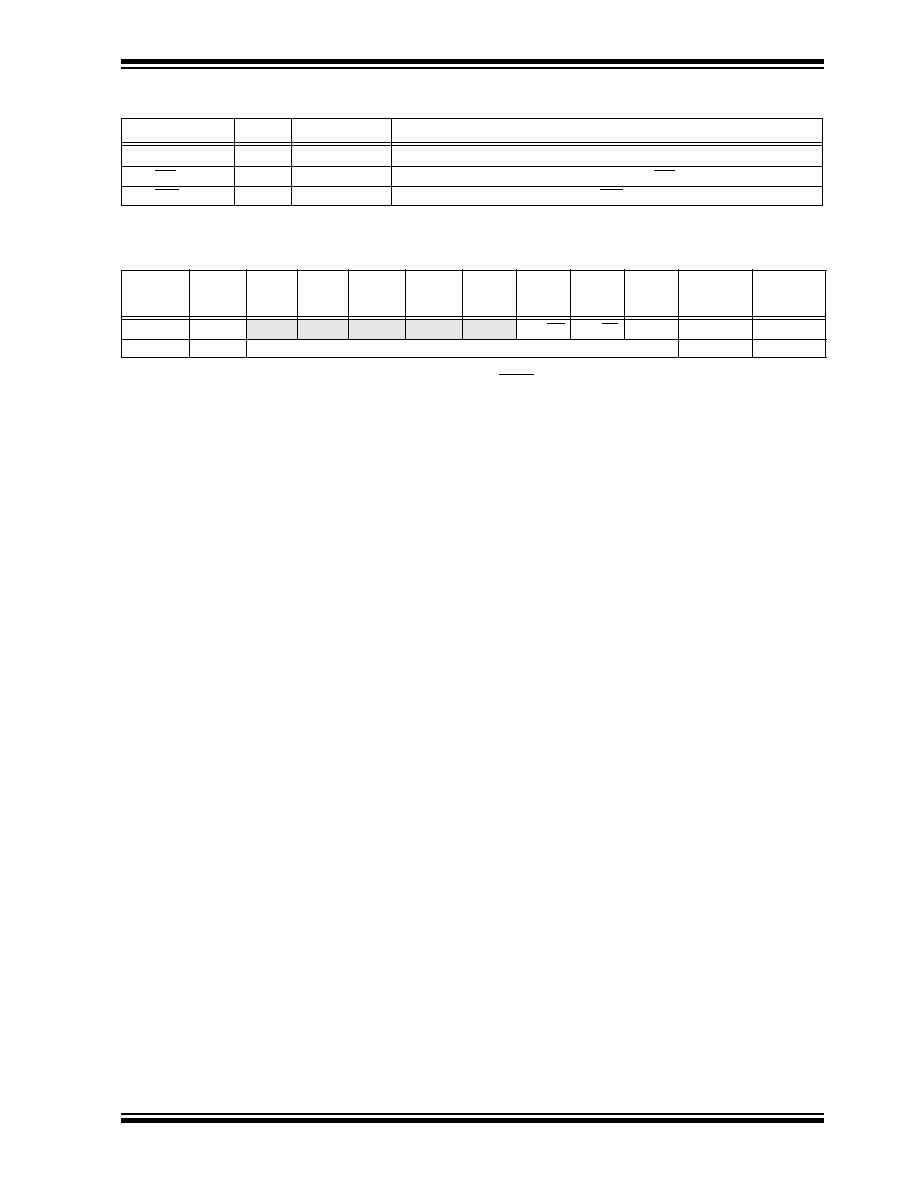
©
1996 Microchip Technology Inc.
DS30412C-page 63
PIC17C4X
TABLE 9-9:
PORTE FUNCTIONS
TABLE 9-10:
REGISTERS/BITS ASSOCIATED WITH PORTE
Name
Bit
Buffer Type
Function
RE0/ALE
bit0
TTL
Input/Output or system bus Address Latch Enable (ALE) control pin.
RE1/OE
bit1
TTL
Input/Output or system bus Output Enable (OE) control pin.
RE2/WR
bit2
TTL
Input/Output or system bus Write (WR) control pin.
Legend: TTL = TTL input.
Address
Name
Bit 7
Bit 6
Bit 5
Bit 4
Bit 3
Bit 2
Bit 1
Bit 0
Value on
Power-on
Reset
Value on all
other resets
(Note1)
15h, Bank 1
PORTE
--
--
--
--
--
RE2/WR RE1/OE RE0/ALE
---- -xxx
---- -uuu
14h, Bank 1
DDRE
Data direction register for PORTE
---- -111
---- -111
Legend:
x
= unknown,
u
= unchanged,
-
= unimplemented read as '0'. Shaded cells are not used by PORTE.
Note 1:
Other (non power-up) resets include: external reset through MCLR and the Watchdog Timer Reset.

PIC17C4X
DS30412C-page 64
©
1996 Microchip Technology Inc.
9.5
I/O Programming Considerations
9.5.1
BI-DIRECTIONAL I/O PORTS
Any instruction which writes, operates internally as a
read followed by a write operation. For example, the
BCF
and
BSF
instructions read the register into the
CPU, execute the bit operation, and write the result
back to the register. Caution must be used when these
instructions are applied to a port with both inputs and
outputs defined. For example, a
BSF
operation on bit5
of PORTB will cause all eight bits of PORTB to be read
into the CPU. Then the
BSF
operation takes place on
bit5 and PORTB is written to the output latches. If
another bit of PORTB is used as a bi-directional I/O pin
(e.g. bit0) and it is defined as an input at this time, the
input signal present on the pin itself would be read into
the CPU and re-written to the data latch of this particu-
lar pin, overwriting the previous content. As long as the
pin stays in the input mode, no problem occurs. How-
ever, if bit0 is switched into output mode later on, the
content of the data latch may now be unknown.
Reading a port reads the values of the port pins. Writing
to the port register writes the value to the port latch.
When using read-modify-write instructions (
BCF, BSF
,
BTG
, etc.) on a port, the value of the port pins is read,
the desired operation is performed with this value, and
the value is then written to the port latch.
Example
9-5 shows the effect of two sequential
read-modify-write instructions on an I/O port.
EXAMPLE 9-5:
READ MODIFY WRITE
INSTRUCTIONS ON AN
I/O PORT
; Initial PORT settings: PORTB<7:4> Inputs
; PORTB<3:0> Outputs
; PORTB<7:6> have pull-ups and are
; not connected to other circuitry
;
; PORT latch PORT pins
; ---------- ---------
;
BCF PORTB, 7 01pp pppp 11pp pppp
BCF PORTB, 6 10pp pppp 11pp pppp
;
BCF DDRB, 7 10pp pppp 11pp pppp
BCF DDRB, 6 10pp pppp 10pp pppp
;
; Note that the user may have expected the
; pin values to be 00pp pppp. The 2nd BCF
; caused RB7 to be latched as the pin value
; (High).
9.5.2
SUCCESSIVE OPERATIONS ON I/O PORTS
The actual write to an I/O port happens at the end of an
instruction cycle, whereas for reading, the data must be
valid at the beginning of the instruction cycle (Figure 9-
9). Therefore, care must be exercised if a write followed
by a read operation is carried out on the same I/O port.
The sequence of instructions should be such to allow
the pin voltage to stabilize (load dependent) before
executing the instruction that reads the values on that
I/O port. Otherwise, the previous state of that pin may
be read into the CPU rather than the "new" state. When
in doubt, it is better to separate these instructions with
a
NOP
or another instruction not accessing this I/O port.
Note:
A pin actively outputting a Low or High
should not be driven from external devices
in order to change the level on this pin (i.e.
"wired-or", "wired-and"). The resulting high
output currents may damage the device.
FIGURE 9-9:
SUCCESSIVE I/O OPERATION
Note:
This example shows a write to PORTB
followed by a read from PORTB.
Note that:
data setup time = (0.25 T
CY
- T
PD
)
where T
CY
= instruction cycle.
Therefore, at higher clock
frequencies, a write followed by a
read may be problematic.
T
PD
= propagation delay
PC
PC + 1
PC + 2
PC + 3
Q1 Q2 Q3 Q4
Q1 Q2 Q3 Q4 Q1 Q2 Q3 Q4
Q1 Q2 Q3 Q4
Instruction
fetched
RB7:RB0
MOVWF PORTB
write to
PORTB
NOP
Port pin
sampled here
NOP
MOVF PORTB,W
Instruction
executed
MOVWF PORTB
write to
PORTB
NOP
MOVF PORTB,W

©
1996 Microchip Technology Inc.
DS30412C-page 65
PIC17C4X
10.0
OVERVIEW OF TIMER
RESOURCES
The PIC17C4X has four timer modules. Each module
can generate an interrupt to indicate that an event has
occurred. These timers are called:
∑ Timer0 - 16-bit timer with programmable 8-bit
prescaler
∑ Timer1 - 8-bit timer
∑ Timer2 - 8-bit timer
∑ Timer3 - 16-bit timer
For enhanced time-base functionality, two input Cap-
tures and two Pulse Width Modulation (PWM) outputs
are possible. The PWMs use the TMR1 and TMR2
resources and the input Captures use the TMR3
resource.
10.1
Timer0 Overview
The Timer0 module is a simple 16-bit overflow counter.
The clock source can be either the internal system
clock (Fosc/4) or an external clock.
The Timer0 module also has a programmable pres-
caler option. The PS3:PS0 bits (T0STA<4:1>) deter-
mine the prescaler value. TMR0 can increment at the
following rates: 1:1, 1:2, 1:4, 1:8, 1:16, 1:32, 1:64,
1:128, 1:256.
When TImer0's clock source is an external clock, the
Timer0 module can be selected to increment on either
the rising or falling edge.
Synchronization of the external clock occurs after the
prescaler. When the prescaler is used, the external
clock frequency may be higher then the device's fre-
quency. The maximum frequency is 50 MHz, given the
high and low time requirements of the clock.
10.2
Timer1 Overview
The TImer0 module is an 8-bit timer/counter with an 8-
bit period register (PR1). When the TMR1 value rolls
over from the period match value to 0h, the TMR1IF
flag is set, and an interrupt will be generated when
enabled. In counter mode, the clock comes from the
RB4/TCLK12 pin, which can also be selected to be the
clock for the Timer2 module.
TMR1 can be concatenated to TMR2 to form a 16-bit
timer. The TMR1 register is the LSB and TMR2 is the
MSB. When in the 16-bit timer mode, there is a corre-
sponding 16-bit period register (PR2:PR1). When the
TMR2:TMR1 value rolls over from the period match
value to 0h, the TMR1IF flag is set, and an interrupt
will be generated when enabled.
10.3
Timer2 Overview
The TMR2 module is an 8-bit timer/counter with an 8-
bit period register (PR2). When the TMR2 value rolls
over from the period match value to 0h, the TMR2IF
flag is set, and an interrupt will be generated when
enabled. In counter mode, the clock comes from the
RB4/TCLK12 pin, which can also be selected to be the
clock for the TMR1 module.
TMR1 can be concatenated to TMR2 to form a 16-bit
timer. The TMR2 register is the MSB and TMR1 is the
LSB. When in the 16-bit timer mode, there is a corre-
sponding 16-bit period register (PR2:PR1). When the
TMR2:TMR1 value rolls over from the period match
value to 0h, the TMR1IF flag is set, and an interrupt
will be generated when enabled.
10.4
Timer3 Overview
The TImer3 module is a 16-bit timer/counter with a 16-
bit period register. When the TMR3H:TMR3L value
rolls over to 0h, the TMR3IF bit is set and an interrupt
will be generated when enabled. In counter mode, the
clock comes from the RB5/TCLK3 pin.
When operating in the dual capture mode, the period
registers become the second 16-bit capture register.
10.5
Role of the Timer/Counters
The timer modules are general purpose, but have ded-
icated resources associated with them. TImer1 and
Timer2 are the time-bases for the two Pulse Width
Modulation (PWM) outputs, while Timer3 is the time-
base for the two input captures.
This document was created with FrameMaker 4 0 4

PIC17C4X
DS30412C-page 66
©
1996 Microchip Technology Inc.
NOTES:

©
1996 Microchip Technology Inc.
DS30412C-page 67
PIC17C4X
11.0
TIMER0
The Timer0 module consists of a 16-bit timer/counter,
TMR0. The high byte is TMR0H and the low byte is
TMR0L. A software programmable 8-bit prescaler
makes an effective 24-bit overflow timer. The clock
source is also software programmable as either the
internal instruction clock or the RA1/T0CKI pin. The
control bits for this module are in register T0STA
(Figure 11-1).
FIGURE 11-1: T0STA REGISTER
(ADDRESS: 05h, UNBANKED)
R/W - 0
R/W - 0
R/W - 0
R/W - 0
R/W - 0
R/W - 0
R/W - 0
U - 0
INTEDG
T0SE
T0CS
PS3
PS2
PS1
PS0
--
R = Readable bit
W = Writable bit
U = Unimplemented,
Read as '0'
-n = Value at POR reset
bit7
bit0
bit 7:
INTEDG
: RA0/INT Pin Interrupt Edge Select bit
This bit selects the edge upon which the interrupt is detected
1 = Rising edge of RA0/INT pin generates interrupt
0 = Falling edge of RA0/INT pin generates interrupt
bit 6:
T0SE
: Timer0 Clock Input Edge Select bit
This bit selects the edge upon which TMR0 will increment
When T0CS = 0
1 = Rising edge of RA1/T0CKI pin increments TMR0 and/or generates a T0CKIF interrupt
0 = Falling edge of RA1/T0CKI pin increments TMR0 and/or generates a T0CKIF interrupt
When T0CS = 1
Don't care
bit 5:
T0CS
: Timer0 Clock Source Select bit
This bit selects the clock source for TMR0.
1 = Internal instruction clock cycle (T
CY
)
0 = T0CKI pin
bit 4-1:
PS3:PS0
: Timer0 Prescale Selection bits
These bits select the prescale value for TMR0.
bit 0:
Unimplemented
: Read as '0'
PS3:PS0
Prescale Value
0000
0001
0010
0011
0100
0101
0110
0111
1xxx
1:1
1:2
1:4
1:8
1:16
1:32
1:64
1:128
1:256
This document was created with FrameMaker 4 0 4

PIC17C4X
DS30412C-page 68
©
1996 Microchip Technology Inc.
11.1
Timer0 Operation
When the T0CS (T0STA<5>) bit is set, TMR0 incre-
ments on the internal clock. When T0CS is clear, TMR0
increments on the external clock (RA1/T0CKI pin). The
external clock edge can be configured in software.
When the T0SE (T0STA<6>) bit is set, the timer will
increment on the rising edge of the RA1/T0CKI pin.
When T0SE is clear, the timer will increment on the fall-
ing edge of the RA1/T0CKI pin. The prescaler can be
programmed to introduce a prescale of 1:1 to 1:256.
The timer increments from 0000h to FFFFh and rolls
over to 0000h. On overflow, the TMR0 Interrupt Flag bit
(T0IF) is set. The TMR0 interrupt can be masked by
clearing the corresponding TMR0 Interrupt Enable bit
(T0IE). The TMR0 Interrupt Flag bit (T0IF) is automati-
cally cleared when vectoring to the TMR0 interrupt vec-
tor.
11.2
Using Timer0 with External Clock
When the external clock input is used for Timer0, it is
synchronized with the internal phase clocks.
Figure 11-3 shows the synchronization of the external
clock. This synchronization is done after the prescaler.
The output of the prescaler (PSOUT) is sampled twice
in every instruction cycle to detect a rising or a falling
edge. The timing requirements for the external clock
are detailed in the electrical specification section for the
desired device.
11.2.1
DELAY FROM EXTERNAL CLOCK EDGE
Since the prescaler output is synchronized with the
internal clocks, there is a small delay from the time the
external clock edge occurs to the time TMR0 is actually
incremented. Figure 11-3 shows that this delay is
between 3T
OSC
and 7T
OSC
. Thus, for example, mea-
suring the interval between two edges (e.g. period) will
be accurate within
±
4T
OSC
(
±
121 ns @ 33 MHz).
FIGURE 11-2: TIMER0 MODULE BLOCK DIAGRAM
FIGURE 11-3: TMR0 TIMING WITH EXTERNAL CLOCK (INCREMENT ON FALLING EDGE)
RA1/T0CKI
Synchronization
Prescaler
(8 stage
async ripple
counter)
T0SE
(T0STA<6>)
Fosc/4
T0CS
(T0STA<5>)
PS3:PS0
(T0STA<4:1>)
Q2
Q4
0
1
TMR0H<8> TMR0L<8>
Interrupt on overflow
sets T0IF
(INTSTA<5>)
4
PSOUT
Q1 Q2 Q3 Q4
Q1 Q2 Q3 Q4
Q1 Q2 Q3 Q4 Q1 Q2 Q3 Q4
Prescaler
output
(PSOUT)
Sampled
Prescaler
output
Increment
TMR0
TMR0
T0
T0 + 1
T0 + 2
(note 3)
(note 2)
Note 1: The delay from the T0CKI edge to the TMR0 increment is 3Tosc to 7Tosc.
2:
= PSOUT is sampled here.
3: The PSOUT high time is too short and is missed by the sampling circuit.
(note 1)
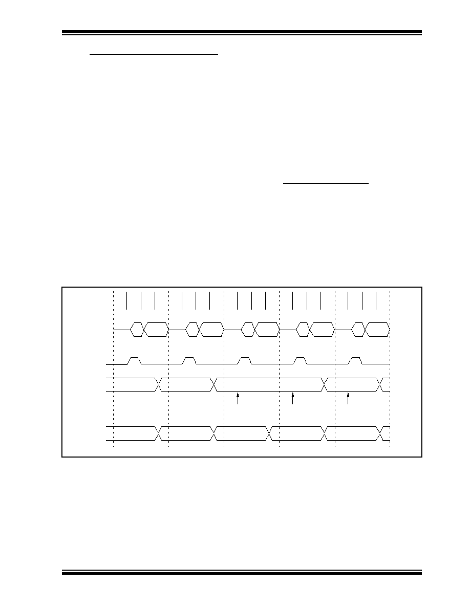
©
1996 Microchip Technology Inc.
DS30412C-page 69
PIC17C4X
11.3
Read/Write Consideration for TMR0
Although TMR0 is a 16-bit timer/counter, only 8-bits at
a time can be read or written during a single instruction
cycle. Care must be taken during any read or write.
11.3.1
READING 16-BIT VALUE
The problem in reading the entire 16-bit value is that
after reading the low (or high) byte, its value may
change from FFh to 00h.
Example 11-1 shows a 16-bit read. To ensure a proper
read, interrupts must be disabled during this routine.
EXAMPLE 11-1: 16-BIT READ
MOVPF TMR0L, TMPLO ;read low tmr0
MOVPF TMR0H, TMPHI ;read high tmr0
MOVFP TMPLO, WREG ;tmplo
->
wreg
CPFSLT TMR0L ;tmr0l < wreg?
RETURN ;no then return
MOVPF TMR0L, TMPLO ;read low tmr0
MOVPF TMR0H, TMPHI ;read high tmr0
RETURN ;return
11.3.2
WRITING A 16-BIT VALUE TO TMR0
Since writing to either TMR0L or TMR0H will effectively
inhibit increment of that half of the TMR0 in the next
cycle (following write), but not inhibit increment of the
other half, the user must write to TMR0L first and
TMR0H next in two consecutive instructions, as shown
in Example 11-2. The interrupt must be disabled. Any
write to either TMR0L or TMR0H clears the prescaler.
EXAMPLE 11-2: 16-BIT WRITE
BSF CPUSTA, GLINTD ; Disable interrupt
MOVFP RAM_L, TMR0L ;
MOVFP RAM_H, TMR0H ;
BCF CPUSTA, GLINTD ; Done, enable interrupt
11.4
Prescaler Assignments
Timer0 has an 8-bit prescaler. The prescaler assign-
ment is fully under software control; i.e., it can be
changed "on the fly" during program execution. When
changing the prescaler assignment, clearing the pres-
caler is recommended before changing assignment.
The value of the prescaler is "unknown," and assigning
a value that is less then the present value makes it dif-
ficult to take this unknown time into account.
FIGURE 11-4: TMR0 TIMING: WRITE HIGH OR LOW BYTE
Q1 Q2 Q3 Q4 Q1 Q2 Q3 Q4
Q1 Q2 Q3 Q4
Q1 Q2 Q3 Q4
Q1 Q2 Q3 Q4
AD15:AD0
ALE
TMR0L
TMR0H
MOVFP W,TMR0L
Write to TMR0L
MOVFP TMR0L,W
Read TMR0L
(Value = NT0)
MOVFP TMR0L,W
Read TMR0L
(Value = NT0)
MOVFP TMR0L,W
Read TMR0L
(Value = NT0 +1)
T0
T0+1
New T0 (NT0)
New T0+1
PC
PC+1
PC+2
PC+3
PC+4
Fetch
Instruction
executed
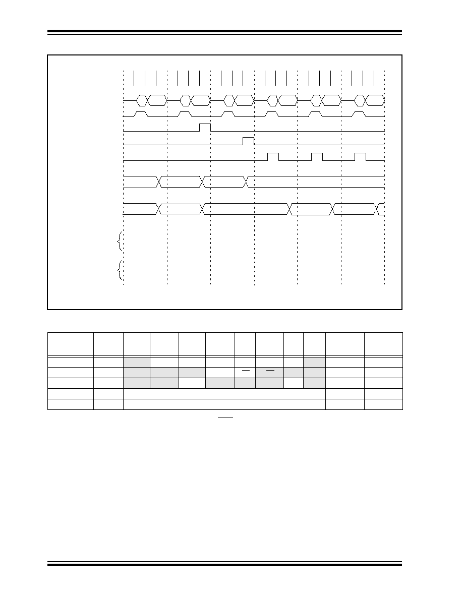
PIC17C4X
DS30412C-page 70
©
1996 Microchip Technology Inc.
FIGURE 11-5: TMR0 READ/WRITE IN TIMER MODE
TABLE 11-1:
REGISTERS/BITS ASSOCIATED WITH TIMER0
Address
Name
Bit 7
Bit 6
Bit 5
Bit 4
Bit 3
Bit 2
Bit 1
Bit 0
Value on
Power-on
Reset
Value on all
other resets
(Note1)
05h, Unbanked
T0STA
INTEDG
T0SE
T0CS
PS3
PS2
PS1
PS0
--
0000 000-
0000 000-
06h, Unbanked
CPUSTA
--
--
STKAV
GLINTD
TO
PD
--
--
--11 11--
--11 qq--
07h, Unbanked
INTSTA
PEIF
T0CKIF
T0IF
INTF
PEIE
T0CKIE
T0IE
INTE
0000 0000
0000 0000
0Bh, Unbanked
TMR0L
TMR0 register; low byte
xxxx xxxx
uuuu uuuu
0Ch, Unbanked
TMR0H
TMR0 register; high byte
xxxx xxxx
uuuu uuuu
Legend:
x
= unknown,
u
= unchanged,
-
= unimplemented read as a '0',
q
- value depends on condition, Shaded cells are not used by Timer0.
Note 1:
Other (non power-up) resets include: external reset through MCLR and the Watchdog Timer Reset.
Instruction
executed
MOVFP
DATAL,TMR0L
Write TMR0L
MOVFP
DATAH,TMR0H
Write TMR0H
MOVPF
TMR0L,W
Read TMR0L
MOVPF
TMR0L,W
Read TMR0L
MOVPF
TMR0L,W
Read TMR0L
Q1
Q2
Q3
Q4
Q1
Q2
Q3
Q4
Q1
Q2
Q3
Q4
Q1
Q2
Q3
Q4
Q1
Q2
Q3
Q4
Q1
Q2
Q3
Q4
AD15:AD0
ALE
WR_TRM0L
WR_TMR0H
RD_TMR0L
TMR0H
TMR0L
12
12
13
AB
FE
FF
56
57
58
In this example, old TMR0 value is 12FEh, new value of AB56h is written.
Instruction
fetched
MOVFP
DATAL,TMR0L
Write TMR0L
MOVFP
DATAH,TMR0H
Write TMR0H
MOVPF
TMR0L,W
Read TMR0L
MOVPF
TMR0L,W
Read TMR0L
MOVPF
TMR0L,W
Read TMR0L
MOVPF
TMR0L,W
Read TMR0L
Previously
Fetched
Instruction

©
1996 Microchip Technology Inc.
DS30412C-page 71
PIC17C4X
12.0
TIMER1, TIMER2, TIMER3,
PWMS AND CAPTURES
The PIC17C4X has a wealth of timers and time-based
functions to ease the implementation of control applica-
tions. These time-base functions include two PWM out-
puts and two Capture inputs.
Timer1 and Timer2 are two 8-bit incrementing timers,
each with a period register (PR1 and PR2 respectively)
and separate overflow interrupt flags. Timer1 and
Timer2 can operate either as timers (increment on
internal Fosc/4 clock) or as counters (increment on fall-
ing edge of external clock on pin RB4/TCLK12). They
are also software configurable to operate as a single
16-bit timer. These timers are also used as the
time-base for the PWM (pulse width modulation) mod-
ule.
Timer3 is a 16-bit timer/counter consisting of the
TMR3H and TMR3L registers. This timer has four other
associated registers. Two registers are used as a 16-bit
period register or a 16-bit Capture1 register
(PR3H/CA1H:PR3L/CA1L). The other two registers are
strictly the Capture2 registers (CA2H:CA2L). Timer3 is
the time-base for the two 16-bit captures.
TMR3 can be software configured to increment from
the internal system clock or from an external signal on
the RB5/TCLK3 pin.
Figure 12-1 and Figure 12-2 are the control registers
for the operation of Timer1, Timer2, and Timer3, as well
as PWM1, PWM2, Capture1, and Capture2.
FIGURE 12-1: TCON1 REGISTER (ADDRESS: 16h, BANK 3)
R/W - 0
R/W - 0
R/W - 0
R/W - 0
R/W - 0
R/W - 0
R/W - 0
R/W - 0
CA2ED1 CA2ED0 CA1ED1 CA1ED0
T16
TMR3CS TMR2CS TMR1CS
R = Readable bit
W = Writable bit
-n = Value at POR reset
bit7
bit0
bit 7-6:
CA2ED1:CA2ED0
: Capture2 Mode Select bits
00 = Capture on every falling edge
01 = Capture on every rising edge
10 = Capture on every 4th rising edge
11 = Capture on every 16th rising edge
bit 5-4:
CA1ED1:CA1ED0
: Capture1 Mode Select bits
00 = Capture on every falling edge
01 = Capture on every rising edge
10 = Capture on every 4th rising edge
11 = Capture on every 16th rising edge
bit 3:
T16
: Timer1:Timer2 Mode Select bit
1 = Timer1 and Timer2 form a 16-bit timer
0 = Timer1 and Timer2 are two 8-bit timers
bit 2:
TMR3CS
: Timer3 Clock Source Select bit
1 = TMR3 increments off the falling edge of the RB5/TCLK3 pin
0 = TMR3 increments off the internal clock
bit 1:
TMR2CS
: Timer2 Clock Source Select bit
1 = TMR2 increments off the falling edge of the RB4/TCLK12 pin
0 = TMR2 increments off the internal clock
bit 0:
TMR1CS
: Timer1 Clock Source Select bit
1 = TMR1 increments off the falling edge of the RB4/TCLK12 pin
0 = TMR1 increments off the internal clock
This document was created with FrameMaker 4 0 4

PIC17C4X
DS30412C-page 72
©
1996 Microchip Technology Inc.
FIGURE 12-2: TCON2 REGISTER (ADDRESS: 17h, BANK 3)
R - 0
R - 0
R/W - 0
R/W - 0
R/W - 0
R/W - 0
R/W - 0
R/W - 0
CA2OVF CA1OVF PWM2ON PWM1ON CA1/PR3 TMR3ON TMR2ON TMR1ON
R = Readable bit
W = Writable bit
-n = Value at POR reset
bit7
bit0
bit 7:
CA2OVF
: Capture2 Overflow Status bit
This bit indicates that the capture value had not been read from the capture register pair (CA2H:CA2L)
before the next capture event occurred. The capture register retains the oldest unread capture value (last
capture before overflow). Subsequent capture events will not update the capture register with the Timer3
value until the capture register has been read (both bytes).
1 = Overflow occurred on Capture2 register
0 = No overflow occurred on Capture2 register
bit 6:
CA1OVF
: Capture1 Overflow Status bit
This bit indicates that the capture value had not been read from the capture register pair
(PR3H/CA2H:PR3L/CA2L) before the next capture event occurred. The capture register retains the old-
est unread capture value (last capture before overflow). Subsequent capture events will not update the
capture register with the TMR3 value until the capture register has been read (both bytes).
1 = Overflow occurred on Capture1 register
0 = No overflow occurred on Capture1 register
bit 5:
PWM2ON
: PWM2 On bit
1 = PWM2 is enabled (The RB3/PWM2 pin ignores the state of the DDRB<3> bit)
0 = PWM2 is disabled (The RB3/PWM2 pin uses the state of the DDRB<3> bit for data direction)
bit 4:
PWM1ON
: PWM1 On bit
1 = PWM1 is enabled (The RB2/PWM1 pin ignores the state of the DDRB<2> bit)
0 = PWM1 is disabled (The RB2/PWM1 pin uses the state of the DDRB<2> bit for data direction)
bit 3:
CA1/PR3
: CA1/PR3 Register Mode Select bit
1 = Enables Capture1 (PR3H/CA1H:PR3L/CA1L is the Capture1 register. Timer3 runs without
a period register)
0 = Enables the Period register (PR3H/CA1H:PR3L/CA1L is the Period register for Timer3)
bit 2:
TMR3ON
: Timer3 On bit
1 = Starts Timer3
0 = Stops Timer3
bit 1:
TMR2ON
: Timer2 On bit
This bit controls the incrementing of the Timer2 register. When Timer2:Timer1 form the 16-bit timer (T16
is set), TMR2ON must be set. This allows the MSB of the timer to increment.
1 = Starts Timer2 (Must be enabled if the T16 bit (TCON1<3>) is set)
0 = Stops Timer2
bit 0:
TMR1ON
: Timer1 On bit
When T16 is set (in 16-bit Timer Mode)
1 = Starts 16-bit Timer2:Timer1
0 = Stops 16-bit Timer2:Timer1
When T16 is clear (in 8-bit Timer Mode)
1 = Starts 8-bit Timer1
0 = Stops 8-bit Timer1

©
1996 Microchip Technology Inc.
DS30412C-page 73
PIC17C4X
12.1
Timer1 and Timer2
12.1.1
TIMER1, TIMER2 IN 8-BIT MODE
Both Timer1 and Timer2 will operate in 8-bit mode
when the T16 bit is clear. These two timers can be inde-
pendently configured to increment from the internal
instruction cycle clock or from an external clock source
on the RB4/TCLK12 pin. The timer clock source is con-
figured by the TMRxCS bit (x = 1 for Timer1 or = 2 for
Timer2). When TMRxCS is clear, the clock source is
internal and increments once every instruction cycle
(Fosc/4). When TMRxCS is set, the clock source is the
RB4/TCLK12 pin, and the timer will increment on every
falling edge of the RB4/TCLK12 pin.
The timer increments from 00h until it equals the Period
register (PRx). It then resets to 00h at the next incre-
ment cycle. The timer interrupt flag is set when the timer
is reset. TMR1 and TMR2 have individual interrupt flag
bits. The TMR1 interrupt flag bit is latched into TMR1IF,
and the TMR2 interrupt flag bit is latched into TMR2IF.
Each timer also has a corresponding interrupt enable
bit (TMRxIE). The timer interrupt can be enabled by set-
ting this bit and disabled by clearing this bit. For periph-
eral interrupts to be enabled, the Peripheral Interrupt
Enable bit must be enabled (PEIE is set) and global
interrupts must be enabled (GLINTD is cleared).
The timers can be turned on and off under software
control. When the Timerx On control bit (TMRxON) is
set, the timer increments from the clock source. When
TMRxON is cleared, the timer is turned off and cannot
cause the timer interrupt flag to be set.
12.1.1.1
EXTERNAL CLOCK INPUT FOR TIMER1
OR TIMER2
When TMRxCS is set, the clock source is the
RB4/TCLK12 pin, and the timer will increment on every
falling edge on the RB4/TCLK12 pin. The TCLK12 input
is synchronized with internal phase clocks. This causes
a delay from the time a falling edge appears on TCLK12
to the time TMR1 or TMR2 is actually incremented. For
the external clock input timing requirements, see the
Electrical Specification section.
FIGURE 12-3: TIMER1 AND TIMER2 IN TWO 8-BIT TIMER/COUNTER MODE
Fosc/4
RB4/TCLK12
TMR1ON
(TCON2<0>)
TMR1CS
(TCON1<0>)
TMR1
PR1
Reset
Equal
Set TMR1IF
(PIR<4>)
0
1
Comparator<8>
Comparator x8
Fosc/4
TMR2ON
(TCON2<1>)
TMR2CS
(TCON1<1>)
TMR2
PR2
Reset
Equal
Set TMR2IF
(PIR<5>)
1
0
Comparator<8>
Comparator x8

PIC17C4X
DS30412C-page 74
©
1996 Microchip Technology Inc.
12.1.2
TIMER1 & TIMER2 IN 16-BIT MODE
To select 16-bit mode, the T16 bit must be set. In this
mode TMR1 and TMR2 are concatenated to form a
16-bit timer (TMR2:TMR1). The 16-bit timer incre-
ments until it matches the 16-bit period register
(PR2:PR1). On the following timer clock, the timer
value is reset to 0h, and the TMR1IF bit is set.
When selecting the clock source for the16-bit timer, the
TMR1CS bit controls the entire 16-bit timer and
TMR2CS is a "don't care." When TMR1CS is clear, the
timer increments once every instruction cycle (Fosc/4).
When TMR1CS is set, the timer increments on every
falling edge of the RB4/TCLK12 pin. For the 16-bit timer
to increment, both TMR1ON and TMR2ON bits must be
set (Table 12-1).
12.1.2.1
EXTERNAL CLOCK INPUT FOR
TMR1:TMR2
When TMR1CS is set, the 16-bit TMR2:TMR1 incre-
ments on the falling edge of clock input TCLK12. The
input on the RB4/TCLK12 pin is sampled and synchro-
nized by the internal phase clocks twice every instruc-
tion cycle. This causes a delay from the time a falling
edge appears on RB4/TCLK12 to the time
TMR2:TMR1 is actually incremented. For the external
clock input timing requirements, see the Electrical
Specification section.
TABLE 12-1:
TURNING ON 16-BIT TIMER
TMR2ON
TMR1ON
Result
1
1
16-bit timer
(TMR2:TMR1) ON
0
1
Only TMR1 increments
x
0
16-bit timer OFF
FIGURE 12-4: TMR1 AND TMR2 IN 16-BIT TIMER/COUNTER MODE
TABLE 12-2:
SUMMARY OF TIMER1 AND TIMER2 REGISTERS
Address
Name
Bit 7
Bit 6
Bit 5
Bit 4
Bit 3
Bit 2
Bit 1
Bit 0
Value on
Power-on
Reset
Value on all
other resets
(Note1)
16h, Bank 3
TCON1
CA2ED1
CA2ED0
CA1ED1
CA1ED0
T16
TMR3CS TMR2CS TMR1CS
0000 0000
0000 0000
17h, Bank 3
TCON2
CA2OVF
CA1OVF PWM2ON PWM1ON CA1/PR3 TMR3ON TMR2ON TMR1ON
0000 0000
0000 0000
10h, Bank 2
TMR1
Timer1 register
xxxx xxxx
uuuu uuuu
11h, Bank 2
TMR2
Timer2 register
xxxx xxxx
uuuu uuuu
16h, Bank 1
PIR
RBIF
TMR3IF
TMR2IF
TMR1IF
CA2IF
CA1IF
TXIF
RCIF
0000 0010
0000 0010
17h, Bank 1
PIE
RBIE
TMR3IE
TMR2IE
TMR1IE
CA2IE
CA1IE
TXIE
RCIE
0000 0000
0000 0000
07h, Unbanked
INTSTA
PEIF
T0CKIF
T0IF
INTF
PEIE
T0CKIE
T0IE
INTE
0000 0000
0000 0000
06h, Unbanked
CPUSTA
--
--
STKAV
GLINTD
TO
PD
--
--
--11 11--
--11 qq--
14h, Bank 2
PR1
Timer1 period register
xxxx xxxx
uuuu uuuu
15h, Bank 2
PR2
Timer2 period register
xxxx xxxx
uuuu uuuu
10h, Bank 3
PW1DCL
DC1
DC0
--
--
--
--
--
--
xx-- ----
uu-- ----
11h, Bank 3
PW2DCL
DC1
DC0
TM2PW2
--
--
--
--
--
xx0- ----
uu0- ----
12h, Bank 3
PW1DCH
DC9
DC8
DC7
DC6
DC5
DC4
DC3
DC2
xxxx xxxx
uuuu uuuu
13h, Bank 3
PW2DCH
DC9
DC8
DC7
DC6
DC5
DC4
DC3
DC2
xxxx xxxx
uuuu uuuu
Legend:
x
= unknown,
u
= unchanged,
-
= unimplemented read as a '0', q - value depends on condition,
shaded cells are not used by Timer1 or Timer2.
Note 1:
Other (non power-up) resets include: external reset through MCLR and WDT Timer Reset.
RB4/TCLK12
Fosc/4
TMR1ON
(TCON2<0>)
TMR1CS
(TCON1<0>)
TMR1 x 8
PR1 x 8
Reset
Equal
Set Interrupt TMR1IF
(PIR<4>)
1
0
Comparator<8>
Comparator x16
TMR2 x 8
PR2 x 8

©
1996 Microchip Technology Inc.
DS30412C-page 75
PIC17C4X
12.1.3
USING PULSE WIDTH MODULATION
(PWM) OUTPUTS WITH TMR1 AND TMR2
Two high speed pulse width modulation (PWM) outputs
are provided. The PWM1 output uses Timer1 as its
time-base, while PWM2 may be software configured to
use either Timer1 or Timer2 as the time-base. The
PWM outputs are on the RB2/PWM1 and RB3/PWM2
pins.
Each PWM output has a maximum resolution of
10-bits. At 10-bit resolution, the PWM output frequency
is 24.4 kHz (@ 25 MHz clock) and at 8-bit resolution the
PWM output frequency is 97.7 kHz. The duty cycle of
the output can vary from 0% to 100%.
Figure 12-5 shows a simplified block diagram of the
PWM module. The duty cycle register is double buff-
ered for glitch free operation. Figure 12-6 shows how a
glitch could occur if the duty cycle registers were not
double buffered.
The user needs to set the PWM1ON bit (TCON2<4>)
to enable the PWM1 output. When the PWM1ON bit is
set, the RB2/PWM1 pin is configured as PWM1 output
and forced as an output irrespective of the data direc-
tion bit (DDRB<2>). When the PWM1ON bit is clear,
the pin behaves as a port pin and its direction is con-
trolled by its data direction bit (DDRB<2>). Similarly,
the PWM2ON (TCON2<5>) bit controls the configura-
tion of the RB3/PWM2 pin.
FIGURE 12-5: SIMPLIFIED PWM BLOCK
DIAGRAM
PWxDCH
Duty Cycle registers
PWxDCL<7:6>
Clear Timer,
PWMx pin and
Latch D.C.
(Slave)
Comparator
TMR2
Comparator
PRy
(Note 1)
R
S
Q
PWMxON
RCy/PWMx
Note 1: 8-bit timer is concatenated with 2-bit internal Q clock
or 2 bits of the prescaler to create 10-bit time-base.
Read
Write
FIGURE 12-6: PWM OUTPUT
0
10
20
30
40
0
PWM
output
Timer
interrupt
Write new
PWM value
Timer interrupt
new PWM value
transferred to slave
Note The dotted line shows PWM output if duty cycle registers were not double buffered.
If the new duty cycle is written after the timer has passed that value, then the PWM does
not reset at all during the current cycle causing a "glitch".
In this example, PWM period = 50. Old duty cycle is 30. New duty cycle value is 10.

PIC17C4X
DS30412C-page 76
©
1996 Microchip Technology Inc.
12.1.3.1
PWM PERIODS
The period of the PWM1 output is determined by
Timer1 and its period register (PR1). The period of the
PWM2 output can be software configured to use either
Timer1 or Timer2 as the time-base. When TM2PW2 bit
(PW2DCL<5>) is clear, the time-base is determined by
TMR1 and PR1. When TM2PW2 is set, the time-base
is determined by Timer2 and PR2.
Running two different PWM outputs on two different
timers allows different PWM periods. Running both
PWMs from Timer1 allows the best use of resources by
freeing Timer2 to operate as an 8-bit timer. Timer1 and
Timer2 can not be used as a 16-bit timer if either PWM
is being used.
The PWM periods can be calculated as follows:
period of PWM1 =[(PR1) + 1] x 4T
OSC
period of PWM2 =[(PR1) + 1] x 4T
OSC
or
[(PR2) + 1] x 4T
OSC
The duty cycle of PWMx is determined by the 10-bit
value DCx<9:0>. The upper 8-bits are from register
PWxDCH and the lower 2-bits are from PWxDCL<7:6>
(PWxDCH:PWxDCL<7:6>). Table
12-3 shows the
maximum PWM frequency (F
PWM
) given the value in
the period register.
The number of bits of resolution that the PWM can
achieve depends on the operation frequency of the
device as well as the PWM frequency (F
PWM
).
Maximum PWM resolution (bits) for a given PWM fre-
quency:
The PWMx duty cycle is as follows:
PWMx Duty Cycle =
(DCx) x T
OSC
where DCx represents the 10-bit value from
PWxDCH:PWxDCL.
If DCx = 0, then the duty cycle is zero. If PRx =
PWxDCH, then the PWM output will be low for one to
four Q-clock (depending on the state of the
PWxDCL<7:6> bits). For a Duty Cycle to be 100%, the
PWxDCH value must be greater then the PRx value.
The duty cycle registers for both PWM outputs are dou-
ble buffered. When the user writes to these registers,
they are stored in master latches. When TMR1 (or
TMR2) overflows and a new PWM period begins, the
master latch values are transferred to the slave latches
and the PWMx pin is forced high.
Note:
For PW1DCH, PW1DCL, PW2DCH and
PW2DCL registers, a write operation
writes to the "master latches" while a read
operation reads the "slave latches". As a
result, the user may not read back what
was just written to the duty cycle registers.
log
(
F
PWM
log (2)
F
OSC
)
bits
=
The user should also avoid any "read-modify-write"
operations on the duty cycle registers, such as:
ADDWF
PW1DCH
. This may cause duty cycle outputs that are
unpredictable.
TABLE 12-3:
PWM FREQUENCY vs.
RESOLUTION AT 25 MHz
12.1.3.2
PWM INTERRUPTS
The PWM module makes use of TMR1 or TMR2 inter-
rupts. A timer interrupt is generated when TMR1 or
TMR2 equals its period register and is cleared to zero.
This interrupt also marks the beginning of a PWM
cycle. The user can write new duty cycle values before
the timer roll-over. The TMR1 interrupt is latched into
the TMR1IF bit and the TMR2 interrupt is latched into
the TMR2IF bit. These flags must be cleared in soft-
ware.
12.1.3.3
EXTERNAL CLOCK SOURCE
The PWMs will operate regardless of the clock source
of the timer. The use of an external clock has ramifica-
tions that must be understood. Because the external
TCLK12 input is synchronized internally (sampled once
per instruction cycle), the time TCLK12 changes to the
time the timer increments will vary by as much as T
CY
(one instruction cycle). This will cause jitter in the duty
cycle as well as the period of the PWM output.
This jitter will be
±
T
CY
, unless the external clock is syn-
chronized with the processor clock. Use of one of the
PWM outputs as the clock source to the TCLKx input,
will supply a synchronized clock.
In general, when using an external clock source for
PWM, its frequency should be much less than the
device frequency (Fosc).
PWM
Frequency
Frequency (kHz)
24.4
48.8
65.104
97.66
390.6
PRx Value
0xFF
0x7F 0x5F
0x3F
0x0F
High
Resolution
10-bit
9-bit
8.5-bit
8-bit
6-bit
Standard
Resolution
8-bit
7-bit
6.5-bit
6-bit
4-bit

©
1996 Microchip Technology Inc.
DS30412C-page 77
PIC17C4X
12.1.3.3.1 MAX RESOLUTION/FREQUENCY FOR
EXTERNAL CLOCK INPUT
The use of an external clock for the PWM time-base
(Timer1 or Timer2) limits the PWM output to a maxi-
mum resolution of 8-bits. The PWxDCL<7:6> bits must
be kept cleared. Use of any other value will distort the
PWM output. All resolutions are supported when inter-
nal clock mode is selected. The maximum attainable
frequency is also lower. This is a result of the timing
requirements of an external clock input for a timer (see
the Electrical Specification section). The maximum
PWM frequency, when the timers clock source is the
RB4/TCLK12 pin, is shown in Table 12-3 (standard res-
olution mode).
12.2
Timer3
Timer3 is a 16-bit timer consisting of the TMR3H and
TMR3L registers. TMR3H is the high byte of the timer
and TMR3L is the low byte. This timer has an associ-
ated 16-bit period register (PR3H/CA1H:PR3L/CA1L).
This period register can be software configured to be a
second 16-bit capture register.
When the TMR3CS bit (TCON1<2>) is clear, the timer
increments every instruction cycle (Fosc/4). When
TMR3CS is set, the timer increments on every falling
edge of the RB5/TCLK3 pin. In either mode, the
TMR3ON bit must be set for the timer to increment.
When TMR3ON is clear, the timer will not increment or
set the TMR3IF bit.
Timer3 has two modes of operation, depending on the
CA1/PR3 bit (TCON2<3>). These modes are:
∑ One capture and one period register mode
∑ Dual capture register mode
The PIC17C4X has up to two 16-bit capture registers
that capture the 16-bit value of TMR3 when events are
detected on capture pins. There are two capture pins
(RB0/CAP1 and RB1/CAP2), one for each capture reg-
ister. The capture pins are multiplexed with PORTB
pins. An event can be:
∑ a rising edge
∑ a falling edge
∑ every 4th rising edge
∑ every 16th rising edge
Each 16-bit capture register has an interrupt flag asso-
ciated with it. The flag is set when a capture is made.
The capture module is truly part of the Timer3 block.
Figure 12-7 and Figure 12-8 show the block diagrams
for the two modes of operation.
TABLE 12-4:
REGISTERS/BITS ASSOCIATED WITH PWM
Address
Name
Bit 7
Bit 6
Bit 5
Bit 4
Bit 3
Bit 2
Bit 1
Bit 0
Value on
Power-on
Reset
Value on all
other
resets
(Note1)
16h, Bank 3
TCON1
CA2ED1
CA2ED0
CA1ED1
CA1ED0
T16
TMR3CS
TMR2CS
TMR1CS
0000 0000
0000 0000
17h, Bank 3
TCON2
CA2OVF
CA1OVF
PWM2ON
PWM1ON
CA1/PR3 TMR3ON
TMR2ON
TMR1ON
0000 0000
0000 0000
10h, Bank 2
TMR1
Timer1 register
xxxx xxxx
uuuu uuuu
11h, Bank 2
TMR2
Timer2 register
xxxx xxxx
uuuu uuuu
16h, Bank 1
PIR
RBIF
TMR3IF
TMR2IF
TMR1IF
CA2IF
CA1IF
TXIF
RCIF
0000 0010
0000 0010
17h, Bank 1
PIE
RBIE
TMR3IE
TMR2IE
TMR1IE
CA2IE
CA1IE
TXIE
RCIE
0000 0000
0000 0000
07h, Unbanked
INTSTA
PEIF
T0CKIF
T0IF
INTF
PEIE
T0CKIE
T0IE
INTE
0000 0000
0000 0000
06h, Unbanked
CPUSTA
--
--
STKAV
GLINTD
TO
PD
--
--
--11 11--
--11 qq--
10h, Bank 3
PW1DCL
DC1
DC0
--
--
--
--
--
--
xx-- ----
uu-- ----
11h, Bank 3
PW2DCL
DC1
DC0
TM2PW2
--
--
--
--
--
xx0- ----
uu0- ----
12h, Bank 3
PW1DCH
DC9
DC8
DC7
DC6
DC5
DC4
DC3
DC2
xxxx xxxx
uuuu uuuu
13h, Bank 3
PW2DCH
DC9
DC8
DC7
DC6
DC5
DC4
DC3
DC2
xxxx xxxx
uuuu uuuu
Legend:
x
= unknown,
u
= unchanged,
-
= unimplemented read as '0',
q
= value depends on conditions,
shaded cells are not used by PWM.

PIC17C4X
DS30412C-page 78
©
1996 Microchip Technology Inc.
12.2.1
ONE CAPTURE AND ONE PERIOD
REGISTER MODE
In this mode registers PR3H/CA1H and PR3L/CA1L
constitute a 16-bit period register. A block diagram is
shown in Figure 12-7. The timer increments until it
equals the period register and then resets to 0000h.
TMR3 Interrupt Flag bit (TMR3IF) is set at this point.
This interrupt can be disabled by clearing the TMR3
Interrupt Enable bit (TMR3IE). TMR3IF must be
cleared in software.
This mode is selected if control bit CA1/PR3 is clear. In
this mode, the Capture1 register, consisting of high
byte (PR3H/CA1H) and low byte (PR3L/CA1L), is con-
figured as the period control register for TMR3.
Capture1 is disabled in this mode, and the correspond-
ing Interrupt bit CA1IF is never set. TMR3 increments
until it equals the value in the period register and then
resets to 0000h.
Capture2 is active in this mode. The CA2ED1 and
CA2ED0 bits determine the event on which capture will
occur. The possible events are:
∑ Capture on every falling edge
∑ Capture on every rising edge
∑ Capture every 4th rising edge
∑ Capture every 16th rising edge
When a capture takes place, an interrupt flag is latched
into the CA2IF bit. This interrupt can be enabled by set-
ting the corresponding mask bit CA2IE. The Peripheral
Interrupt Enable bit (PEIE) must be set and the Global
Interrupt Disable bit (GLINTD) must be cleared for the
interrupt to be acknowledged. The CA2IF interrupt flag
bit must be cleared in software.
When the capture prescale select is changed, the pres-
caler is not reset and an event may be generated.
Therefore, the first capture after such a change will be
ambiguous. However, it sets the time-base for the next
capture. The prescaler is reset upon chip reset.
Capture pin RB1/CAP2 is a multiplexed pin. When used
as a port pin, Capture2 is not disabled. However, the
user can simply disable the Capture2 interrupt by clear-
ing CA2IE. If RB1/CAP2 is used as an output pin, the
user can activate a capture by writing to the port pin.
This may be useful during development phase to emu-
late a capture interrupt.
The input on capture pin RB1/CAP2 is synchronized
internally to internal phase clocks. This imposes certain
restrictions on the input waveform (see the Electrical
Specification section for timing).
The Capture2 overflow status flag bit is double buff-
ered. The master bit is set if one captured word is
already residing in the Capture2 register and another
"event" has occurred on the RB1/CA2 pin. The new
event will not transfer the Timer3 value to the capture
register, protecting the previous unread capture value.
When the user reads both the high and the low bytes (in
any order) of the Capture2 register, the master overflow
bit is transferred to the slave overflow bit (CA2OVF) and
then the master bit is reset. The user can then read
TCON2 to determine the value of CA2OVF.
The recommended sequence to read capture registers
and capture overflow flag bits is shown in
Example 12-1.
EXAMPLE 12-1: SEQUENCE TO READ
CAPTURE REGISTERS
MOVLB 3 ;Select Bank 3
MOVPF CA2L,LO_BYTE ;Read Capture2 low
;byte, store in LO_BYTE
MOVPF CA2H,HI_BYTE ;Read Capture2 high
;byte, store in HI_BYTE
MOVPF TCON2,STAT_VAL ;Read TCON2 into file
;STAT_VAL
FIGURE 12-7: TIMER3 WITH ONE CAPTURE AND ONE PERIOD REGISTER BLOCK DIAGRAM
PR3H/CA1H
TMR3H
Comparator<8>
Fosc/4
TMR3ON
Reset
Equal
0
1
Comparator x16
RB5/TCLK3
Set TMR3IF
TMR3CS
PR3L/CA1L
TMR3L
CA2H
CA2L
RB1/CAP2
Edge select
prescaler select
2
Set CA2IF
Capture1 Enable
CA2ED1: CA2ED0
(TCON1<7:6>)
(TCON2<2>)
(TCON1<2>)
(PIR<3>)
(PIR<6>)

©
1996 Microchip Technology Inc.
DS30412C-page 79
PIC17C4X
12.2.2
DUAL CAPTURE REGISTER MODE
This mode is selected by setting CA1/PR3. A block dia-
gram is shown in Figure 12-8. In this mode, TMR3 runs
without a period register and increments from 0000h to
FFFFh and rolls over to 0000h. The TMR3 interrupt
Flag (TMR3IF) is set on this roll over. The TMR3IF bit
must be cleared in software.
Registers PR3H/CA1H and PR3L/CA1L make a 16-bit
capture register (Capture1). It captures events on pin
RB0/CAP1. Capture mode is configured by the
CA1ED1 and CA1ED0 bits. Capture1 Interrupt Flag bit
(CA1IF) is set on the capture event. The corresponding
interrupt mask bit is CA1IE. The Capture1 Overflow
Status bit is CA1OVF.
The Capture2 overflow status flag bit is double buff-
ered. The master bit is set if one captured word is
already residing in the Capture2 register and another
"event" has occurred on the RB1/CA2 pin. The new
event will not transfer the TMR3 value to the capture
register which protects the previous unread capture
value. When the user reads both the high and the low
bytes (in any order) of the Capture2 register, the master
overflow bit is transferred to the slave overflow bit
(CA2OVF) and then the master bit is reset. The user
can then read TCON2 to determine the value of
CA2OVF.
The operation of the Capture1 feature is identical to
Capture2 (as described in Section 12.2.1).
FIGURE 12-8: TIMER3 WITH TWO CAPTURE REGISTERS BLOCK DIAGRAM
TABLE 12-5:
REGISTERS ASSOCIATED WITH CAPTURE
Address
Name
Bit 7
Bit 6
Bit 5
Bit 4
Bit 3
Bit 2
Bit 1
Bit 0
Value on
Power-on
Reset
Value on all
other resets
(Note1)
16h, Bank 3
TCON1
CA2ED1
CA2ED0
CA1ED1
CA1ED0
T16
TMR3CS TMR2CS TMR1CS
0000 0000
0000 0000
17h, Bank 3
TCON2
CA2OVF CA1OVF
PWM2ON
PWM1ON CA1/PR3 TMR3ON TMR2ON TMR1ON
0000 0000
0000 0000
12h, Bank 2
TMR3L
TMR3 register; low byte
xxxx xxxx
uuuu uuuu
13h, Bank 2
TMR3H
TMR3 register; high byte
xxxx xxxx
uuuu uuuu
16h, Bank 1
PIR
RBIF
TMR3IF
TMR2IF
TMR1IF
CA2IF
CA1IF
TXIF
RCIF
0000 0010
0000 0010
17h, Bank 1
PIE
RBIE
TMR3IE
TMR2IE
TMR1IE
CA2IE
CA1IE
TXIE
RCIE
0000 0000
0000 0000
07h, Unbanked INTSTA
PEIF
T0CKIF
T0IF
INTF
PEIE
T0CKIE
T0IE
INTE
0000 0000
0000 0000
06h, Unbanked CPUSTA
--
--
STKAV
GLINTD
TO
PD
--
--
--11 11--
--11 qq--
16h, Bank 2
PR3L/CA1L
Timer3 period register, low byte/capture1 register, low byte
xxxx xxxx
uuuu uuuu
17h, Bank 2
PR3H/CA1H Timer3 period register, high byte/capture1 register, high byte
xxxx xxxx
uuuu uuuu
14h, Bank 3
CA2L
Capture2 low byte
xxxx xxxx
uuuu uuuu
15h, Bank 3
CA2H
Capture2 high byte
xxxx xxxx
uuuu uuuu
Legend:
x
= unknown,
u
= unchanged,
-
= unimplemented read as '0',
q
- value depends on condition,
shaded cells are not used by Capture.
Note 1:
Other (non power-up) resets include: external reset through MCLR and WDT Timer Reset.
2
RB0/CAP1
Edge Select
Prescaler Select
PR3H/CA1H
PR3L/CA1L
TMR3H
TMR3L
RB5/TCLK3
0
1
Fosc/4
RB1/CAP2
Edge Select
Prescaler Select
2
CA2ED1, CA2ED0
(TCON1<7:6>)
CA2H
CA2L
Set CA2IF
(PIR<3>)
Set TMR3IF
(PIR<6>)
Set CA1IF
(PIR<2>)
Capture Enable
Capture Enable
TMR3ON
(TCON2<2>)
TMR3CS
(TCON1<2>)
CA1ED1, CA1ED0
(TCON1<5:4>)

PIC17C4X
DS30412C-page 80
©
1996 Microchip Technology Inc.
12.2.3
EXTERNAL CLOCK INPUT FOR TIMER3
When TMR3CS is set, the 16-bit TMR3 increments on
the falling edge of clock input TCLK3. The input on the
RB5/TCLK3 pin is sampled and synchronized by the
internal phase clocks twice every instruction cycle. This
causes a delay from the time a falling edge appears on
TCLK3 to the time TMR3 is actually incremented. For
the external clock input timing requirements, see the
Electrical Specification section. Figure 12-9 shows the
timing diagram when operating from an external clock.
12.2.4
READING/WRITING TIMER3
Since Timer3 is a 16-bit timer and only 8-bits at a time
can be read or written, care should be taken when
reading or writing while the timer is running. The best
method to read or write the timer is to stop the timer,
perform any read or write operation, and then restart
Timer3 (using the TMR3ON bit). However, if it is neces-
sary to keep Timer3 free-running, care must be taken.
For writing to the 16-bit TMR3, Example 12-2 may be
used. For reading the 16-bit TMR3, Example 12-3 may
be used. Interrupts must be disabled during this rou-
tine.
EXAMPLE 12-2: WRITING TO TMR3
BSF CPUSTA, GLINTD ;Disable interrupt
MOVFP RAM_L, TMR3L ;
MOVFP RAM_H, TMR3H ;
BCF CPUSTA, GLINTD ;Done,enable interrupt
EXAMPLE 12-3: READING FROM TMR3
MOVPF TMR3L, TMPLO ;read low tmr0
MOVPF TMR3H, TMPHI ;read high tmr0
MOVFP TMPLO, WREG ;tmplo
->
wreg
CPFSLT TMR3L, WREG ;tmr0l < wreg?
RETURN ;no then return
MOVPF TMR3L, TMPLO ;read low tmr0
MOVPF TMR3H, TMPHI ;read high tmr0
RETURN ;return
FIGURE 12-9: TMR1, TMR2, AND TMR3 OPERATION IN EXTERNAL CLOCK MODE
Q1 Q2 Q3 Q4 Q1 Q2 Q3 Q4 Q1 Q2 Q3 Q4 Q1 Q2 Q3 Q4 Q1 Q2 Q3 Q4 Q1 Q2 Q3 Q4
Instruction
executed
MOVWF
MOVFP
TMRx,W
TMRx
MOVFP
TMRx,W
Write to TMRx
Read TMRx
Read TMRx
34h
35h
A8h
A9h
00h
'A9h'
'A9h'
TCLK12
TMR1, TMR2, or TMR3
PR1, PR2, or PR3H:PR3L
WR_TMR
Read_TMR
TMRxIF
Note 1: TCLK12 is sampled in Q2 and Q4.
2:
indicates a sampling point.
3: The latency from TCLK12
to timer increment is between 2Tosc and 6Tosc.

©
1996 Microchip Technology Inc.
DS30412C-page 81
PIC17C4X
FIGURE 12-10: TMR1, TMR2, AND TMR3 OPERATION IN TIMER MODE
TABLE 12-6:
SUMMARY OF TMR1, TMR2, AND TMR3 REGISTERS
Address
Name
Bit 7
Bit 6
Bit 5
Bit 4
Bit 3
Bit 2
Bit 1
Bit 0
Value on
Power-on
Reset
Value on all
other resets
(Note1)
16h, Bank 3
TCON1
CA2ED1
CA2ED0
CA1ED1
CA1ED0
T16
TMR3CS TMR2CS TMR1CS
0000 0000
0000 0000
17h, Bank 3
TCON2
CA2OVF
CA1OVF PWM2ON PWM1ON CA1/PR3 TMR3ON TMR2ON TMR1ON
0000 0000
0000 0000
10h, Bank 2
TMR1
Timer1 register
xxxx xxxx
uuuu uuuu
11h, Bank 2
TMR2
Timer2 register
xxxx xxxx
uuuu uuuu
12h, Bank 2
TMR3L
TMR3 register; low byte
xxxx xxxx
uuuu uuuu
13h, Bank 2
TMR3H
TMR3 register; high byte
xxxx xxxx
uuuu uuuu
16h, Bank 1
PIR
RBIF
TMR3IF
TMR2IF
TMR1IF
CA2IF
CA1IF
TXIF
RCIF
0000 0010
0000 0010
17h, Bank 1
PIE
RBIE
TMR3IE
TMR2IE
TMR1IE
CA2IE
CA1IE
TXIE
RCIE
0000 0000
0000 0000
07h, Unbanked
INTSTA
PEIF
T0CKIF
T0IF
INTF
PEIE
T0CKIE
T0IE
INTE
0000 0000
0000 0000
06h, Unbanked
CPUSTA
--
--
STKAV
GLINTD
TO
PD
--
--
--11 11--
--11 qq--
14h, Bank 2
PR1
Timer1 period register
xxxx xxxx
uuuu uuuu
15h, Bank 2
PR2
Timer2 period register
xxxx xxxx
uuuu uuuu
16h, Bank 2
PR3L/CA1L
Timer3 period/capture1 register; low byte
xxxx xxxx
uuuu uuuu
17h, Bank 2
PR3H/CA1H Timer3 period/capture1 register; high byte
xxxx xxxx
uuuu uuuu
10h, Bank 3
PW1DCL
DC1
DC0
--
--
--
--
--
--
xx-- ----
uu-- ----
11h, Bank 3
PW2DCL
DC1
DC0
TM2PW2
--
--
--
--
--
xx0- ----
uu0- ----
12h, Bank 3
PW1DCH
DC9
DC8
DC7
DC6
DC5
DC4
DC3
DC2
xxxx xxxx
uuuu uuuu
13h, Bank 3
PW2DCH
DC9
DC8
DC7
DC6
DC5
DC4
DC3
DC2
xxxx xxxx
uuuu uuuu
14h, Bank 3
CA2L
Capture2 low byte
xxxx xxxx
uuuu uuuu
15h, Bank 3
CA2H
Capture2 high byte
xxxx xxxx
uuuu uuuu
Legend:
x
= unknown,
u
= unchanged,
-
= unimplemented read as '0',
q
- value depends on condition,
shaded cells are not used by TMR1, TMR2 or TMR3.
Note 1:
Other (non power-up) resets include: external reset through MCLR and WDT Timer Reset.
Q1Q2 Q3 Q4 Q1Q2 Q3 Q4 Q1Q2 Q3 Q4 Q1Q2 Q3 Q4 Q1Q2 Q3 Q4 Q1Q2 Q3 Q4 Q1Q2 Q3 Q4 Q1Q2 Q3 Q4 Q1Q2 Q3 Q4 Q1Q2 Q3 Q4 Q1Q2 Q3 Q4
AD15:AD0
ALE
Instruction
fetched
TMR1
PR1
TMR1ON
WR_TMR1
WR_TCON2
TMR1IF
RD_TMR1
TMR1
reads 03h
TMR1
reads 04h
MOVWF
TMR1
Write TMR1
MOVF
TMR1, W
Read TMR1
MOVF
TMR1, W
Read TMR1
BSF
TCON2, 0
Stop TMR1
BCF
TCON2, 0
Start TMR1
MOVLB
3
NOP
NOP
NOP
NOP
NOP
04h
05h
03h
04h
05h
06h
07h
08h
00h

PIC17C4X
DS30412C-page 82
©
1996 Microchip Technology Inc.
NOTES:

©
1996 Microchip Technology Inc.
DS30412C-page 83
PIC17C4X
13.0
UNIVERSAL SYNCHRONOUS
ASYNCHRONOUS RECEIVER
TRANSMITTER (USART)
MODULE
The USART module is a serial I/O module. The USART
can be configured as a full duplex asynchronous sys-
tem that can communicate with peripheral devices such
as CRT terminals and personal computers, or it can be
configured as a half duplex synchronous system that
can communicate with peripheral devices such as A/D
or D/A integrated circuits, Serial EEPROMs etc. The
USART can be configured in the following modes:
∑ Asynchronous (full duplex)
∑ Synchronous - Master (half duplex)
∑ Synchronous - Slave (half duplex)
The SPEN (RCSTA<7>) bit has to be set in order to
configure RA4 and RA5 as the Serial Communication
Interface.
The USART module will control the direction of the
RA4/RX/DT and RA5/TX/CK pins, depending on the
states of the USART configuration bits in the RCSTA
and TXSTA registers. The bits that control I/O direction
are:
∑ SPEN
∑ TXEN
∑ SREN
∑ CREN
∑ CSRC
The Transmit Status And Control Register is shown in
Figure 13-1, while the Receive Status And Control
Register is shown in Figure 13-2.
FIGURE 13-1: TXSTA REGISTER (ADDRESS: 15h, BANK 0)
R/W - 0
R/W - 0
R/W - 0
R/W - 0
U - 0
U - 0
R - 1
R/W - x
CSRC
TX9
TXEN
SYNC
--
--
TRMT
TX9D
R = Readable bit
W = Writable bit
-n = Value at POR reset
(x = unknown)
bit7
bit0
bit 7:
CSRC
: Clock Source Select bit
Synchronous mode:
1 = Master Mode (Clock generated internally from BRG)
0 = Slave mode (Clock from external source)
Asynchronous mode:
Don't care
bit 6:
TX9
: 9-bit Transmit Enable bit
1 = Selects 9-bit transmission
0 = Selects 8-bit transmission
bit 5:
TXEN
: Transmit Enable bit
1 = Transmit enabled
0 = Transmit disabled
SREN/CREN overrides TXEN in SYNC mode
bit 4:
SYNC
: USART mode Select bit
(Synchronous/Asynchronous)
1 = Synchronous mode
0 = Asynchronous mode
bit 3-2:
Unimplemented
: Read as '0'
bit 1:
TRMT
: Transmit Shift Register (TSR) Empty bit
1 = TSR empty
0 = TSR full
bit 0:
TX9D
: 9th bit of transmit data (can be used to calculated the parity in software)
This document was created with FrameMaker 4 0 4

PIC17C4X
DS30412C-page 84
©
1996 Microchip Technology Inc.
FIGURE 13-2: RCSTA REGISTER (ADDRESS: 13h, BANK 0)
R/W - 0
R/W - 0
R/W - 0
R/W - 0
U - 0
R - 0
R - 0
R - x
SPEN
RX9
SREN
CREN
--
FERR
OERR
RX9D
R = Readable bit
W = Writable bit
-n = Value at POR reset
(x = unknown)
bit7
bit 0
bit 7:
SPEN
: Serial Port Enable bit
1 = Configures RA5/RX/DT and RA4/TX/CK pins as serial port pins
0 = Serial port disabled
bit 6:
RX9
: 9-bit Receive Enable bit
1 = Selects 9-bit reception
0 = Selects 8-bit reception
bit 5:
SREN
: Single Receive Enable bit
This bit enables the reception of a single byte. After receiving the byte, this bit is automatically cleared.
Synchronous mode:
1 = Enable reception
0 = Disable reception
Note: This bit is ignored in synchronous slave reception.
Asynchronous mode:
Don't care
bit 4:
CREN
: Continuous Receive Enable bit
This bit enables the continuous reception of serial data.
Asynchronous mode:
1 = Enable reception
0 = Disables reception
Synchronous mode:
1 = Enables continuous reception until CREN is cleared (CREN overrides SREN)
0 = Disables continuous reception
bit 3:
Unimplemented
: Read as '0'
bit 2:
FERR
: Framing Error bit
1 = Framing error (Updated by reading RCREG)
0 = No framing error
bit 1:
OERR
: Overrun Error bit
1 = Overrun (Cleared by clearing CREN)
0 = No overrun error
bit 0:
RX9D
: 9th bit of receive data (can be the software calculated parity bit)

©
1996 Microchip Technology Inc.
DS30412C-page 85
PIC17C4X
FIGURE 13-3: USART TRANSMIT
FIGURE 13-4: USART RECEIVE
CK/TX
DT
Sync/Async
TSR
Start 0 1
7 8 Stop
∑ ∑ ∑
˜
16
˜
4
BRG
0 1
7
∑ ∑ ∑
8
Bit Count
TXIE
Interrupt
TXEN/
Write to TXREG
Clock
Sync/Async
Sync/Async
TXSTA<0>
Sync
Master/Slave
Data Bus
Load
TXREG
CK
RX
0
1
7
8
Stop
∑ ∑ ∑
˜
16
˜
4
BRG
Bit Count
Clock
Buffer
Logic
Buffer
Logic
SPEN
OSC
START
0
1
7
RX9D
∑ ∑ ∑
0
1
7
RX9D
∑ ∑ ∑
FERR
FERR
Majority
Detect
Data
MSb
LSb
RSR
RCREG
Async/Sync
Sync/Async
Master/Slave
Sync
enable
FIFO
Logic
Clk
FIFO
RCIE
Interrupt
RX9
Data Bus
SREN/
CREN/
Start_Bit
Async/Sync
Detect
PIC17C4X
DS30412C-page 86
©
1996 Microchip Technology Inc.
13.1
USART Baud Rate Generator (BRG)
The BRG supports both the Asynchronous and Syn-
chronous modes of the USART. It is a dedicated 8-bit
baud rate generator. The SPBRG register controls the
period of a free running 8-bit timer. Table 13-1 shows
the formula for computation of the baud rate for differ-
ent USART modes. These only apply when the USART
is in synchronous master mode (internal clock) and
asynchronous mode.
Given the desired baud rate and Fosc, the nearest inte-
ger value between 0 and 255 can be calculated using
the formula below. The error in baud rate can then be
determined.
TABLE 13-1:
BAUD RATE FORMULA
SYNC
Mode
Baud Rate
0
1
Asynchronous
Synchronous
F
OSC
/(64(X+1))
F
OSC
/(4(X+1))
X = value in SPBRG (0 to 255)
Example 13-1 shows the calculation of the baud rate
error for the following conditions:
F
OSC
= 16 MHz
Desired Baud Rate = 9600
SYNC = 0
EXAMPLE 13-1: CALCULATING BAUD
RATE ERROR
Writing a new value to the SPBRG, causes the BRG
timer to be reset (or cleared), this ensures that the BRG
does not wait for a timer overflow before outputting the
new baud rate.
Desired Baud rate=Fosc / (64 (X + 1))
9600 =
16000000 /(64 (X + 1))
X
=
25.042 = 25
Calculated Baud Rate=16000000 / (64 (25 + 1))
=
9615
Error =
(Calculated Baud Rate - Desired Baud Rate)
Desired Baud Rate
=
(9615 - 9600) / 9600
=
0.16%
TABLE 13-2:
REGISTERS ASSOCIATED WITH BAUD RATE GENERATOR
Address
Name
Bit 7
Bit 6
Bit 5
Bit 4
Bit 3
Bit 2
Bit 1
Bit 0
Value on
Power-on
Reset
Value on all
other resets
(Note1)
13h, Bank 0
RCSTA
SPEN
RX9
SREN
CREN
--
FERR
OERR
RX9D
0000 -00x
0000 -00u
15h, Bank 0
TXSTA
CSRC
TX9
TXEN
SYNC
--
--
TRMT
TX9D
0000 --1x
0000 --1u
17h, Bank 0
SPBRG
Baud rate generator register
xxxx xxxx
uuuu uuuu
Legend:
x
= unknown,
u
= unchanged,
-
= unimplemented read as a '0', shaded cells are not used by the Baud Rate Generator.
Note 1:
Other (non power-up) resets include: external reset through MCLR and Watchdog Timer Reset.

©
1996 Microchip Technology Inc.
DS30412C-page 87
PIC17C4X
TABLE 13-3:
BAUD RATES FOR SYNCHRONOUS MODE
BAUD
RATE
(K)
F
OSC
= 33 MHz
SPBRG
value
(decimal)
F
OSC
= 25 MHz
SPBRG
value
(decimal)
F
OSC
= 20 MHz
SPBRG
value
(decimal)
F
OSC
= 16 MHz
SPBRG
value
(decimal)
KBAUD
%ERROR
KBAUD
%ERROR
KBAUD
%ERROR
KBAUD
%ERROR
0.3
NA
--
--
NA
--
--
NA --
--
NA --
--
1.2
NA
--
--
NA
--
--
NA --
--
NA --
--
2.4
NA
--
--
NA
--
--
NA --
--
NA --
--
9.6
NA
--
--
NA
--
--
NA --
--
NA --
--
19.2
NA
--
--
NA
--
--
19.53
+1.73
255
19.23
+0.16
207
76.8
77.10
+0.39
106
77.16
+0.47
80
76.92
+0.16
64
76.92
+0.16
51
96
95.93
-0.07
85
96.15
+0.16
64
96.15
+0.16
51
95.24
-0.79
41
300
294.64
-1.79
27
297.62
-0.79
20
294.1
-1.96
16
307.69
+2.56
12
500
485.29
-2.94
16
480.77
-3.85
12
500
0
9
500
0
7
HIGH
8250
--
0
6250
--
0
5000
--
0
4000
--
0
LOW 32.22
--
255
24.41
--
255
19.53
--
255
15.625
--
255
BAUD
RATE
(K)
F
OSC
= 10 MHz
SPBRG
value
(decimal)
F
OSC
= 7.159 MHz
SPBRG
value
(decimal)
F
OSC
= 5.068 MHz
SPBRG
value
(decimal)
KBAUD
%ERROR
KBAUD
%ERROR
KBAUD
%ERROR
0.3
NA
--
--
NA --
--
NA --
--
1.2
NA
--
--
NA --
--
NA --
--
2.4
NA
--
--
NA --
--
NA --
--
9.6 9.766
+1.73
255
9.622
+0.23
185
9.6
0
131
19.2
19.23
+0.16
129
19.24
+0.23
92
19.2
0
65
76.8
75.76
-1.36
32
77.82
+1.32
22
79.2
+3.13
15
96
96.15
+0.16
25
94.20
-1.88
18
97.48
+1.54
12
300
312.5
+4.17
7
298.3
-0.57
5
316.8
+5.60
3
500
500
0
4
NA
--
--
NA
--
--
HIGH
2500
--
0
1789.8
--
0
1267
--
0
LOW 9.766
--
255
6.991
--
255
4.950
--
255
BAUD
RATE
(K)
F
OSC
= 3.579 MHz
SPBRG
value
(decimal)
F
OSC
= 1 MHz
SPBRG
value
(decimal)
F
OSC
= 32.768 kHz
SPBRG
value
(decimal)
KBAUD
%ERROR
KBAUD
%ERROR
KBAUD
%ERROR
0.3
NA
--
--
NA --
--
0.303
+1.14
26
1.2
NA
--
--
1.202 +0.16
207
1.170
-2.48
6
2.4
NA
--
--
2.404
+0.16
103
NA --
--
9.6 9.622
+0.23
92
9.615
+0.16
25
NA --
--
19.2
19.04
-0.83
46
19.24
+0.16
12
NA --
--
76.8
74.57
-2.90
11
83.34
+8.51
2
NA --
--
96
99.43
_3.57
8
NA --
--
NA --
--
300
298.3
-0.57
2
NA --
--
NA --
--
500
NA --
--
NA --
--
NA --
--
HIGH
894.9
--
0
250
--
0
8.192
--
0
LOW 3.496
--
255
0.976
--
255
0.032
--
255

PIC17C4X
DS30412C-page 88
©
1996 Microchip Technology Inc.
TABLE 13-4:
BAUD RATES FOR ASYNCHRONOUS MODE
BAUD
RATE
(K)
F
OSC
= 33 MHz
SPBRG
value
(decimal)
F
OSC
= 25 MHz
SPBRG
value
(decimal)
F
OSC
= 20 MHz
SPBRG
value
(decimal)
F
OSC
= 16 MHz
SPBRG
value
(decimal)
KBAUD
%ERROR
KBAUD
%ERROR
KBAUD
%ERROR
KBAUD
%ERROR
0.3
NA
--
--
NA
--
--
NA --
--
NA --
--
1.2
NA
--
--
NA
--
--
1.221
+1.73
255
1.202
+0.16
207
2.4
2.398
-0.07
214
2.396
0.14
162
2.404
+0.16
129
2.404
+0.16
103
9.6 9.548
-0.54
53
9.53
-0.76
40
9.469
-1.36
32
9.615
+0.16
25
19.2
19.09
-0.54
26
19.53
+1.73
19
19.53
+1.73
15
19.23
+0.16
12
76.8
73.66
-4.09
6
78.13
+1.73
4
78.13
+1.73
3
83.33
+8.51
2
96
103.12
+7.42
4
97.65
+1.73
3
104.2
+8.51
2
NA
--
--
300
257.81
-14.06
1
390.63
+30.21
0
312.5
+4.17
0
NA
--
--
500
515.62
+3.13
0
NA
--
--
NA
--
--
NA
--
--
HIGH
515.62
--
0
--
--
0
312.5
--
0
250
--
0
LOW 2.014
--
255
1.53
--
255
1.221
--
255
0.977
--
255
BAUD
RATE
(K)
F
OSC
= 10 MHz
SPBRG
value
(decimal)
F
OSC
= 7.159 MHz
SPBRG
value
(decimal)
F
OSC
= 5.068 MHz
SPBRG
value
(decimal)
KBAUD
%ERROR
KBAUD
%ERROR
KBAUD
%ERROR
0.3
NA
--
--
NA --
--
0.31
+3.13
255
1.2
1.202
+0.16
129
1.203
_0.23
92
1.2
0
65
2.4
2.404
+0.16
64
2.380
-0.83
46
2.4
0
32
9.6 9.766
+1.73
15
9.322
-2.90
11
9.9
-3.13
7
19.2
19.53
+1.73
7
18.64
-2.90
5
19.8
+3.13
3
76.8
78.13
+1.73
1
NA
--
--
79.2
+3.13
0
96
NA
--
--
NA
--
--
NA
--
--
300
NA
--
--
NA
--
--
NA
--
--
500
NA
--
--
NA
--
--
NA
--
--
HIGH
156.3
--
0
111.9
--
0
79.2
--
0
LOW 0.610
--
255
0.437
--
255
0.309
--
2
55
BAUD
RATE
(K)
F
OSC
= 3.579 MHz
SPBRG
value
(decimal)
F
OSC
= 1 MHz
SPBRG
value
(decimal)
F
OSC
= 32.768 kHz
SPBRG
value
(decimal)
KBAUD
%ERROR
KBAUD
%ERROR
KBAUD
%ERROR
0.3
0.301
+0.23
185
0.300
+0.16
51
0.256
-14.67
1
1.2
1.190
-0.83
46
1.202
+0.16
12
NA
--
--
2.4
2.432
+1.32
22
2.232
-6.99
6
NA
--
--
9.6 9.322
-2.90
5
NA
--
--
NA
--
--
19.2
18.64
-2.90
2
NA
--
--
NA
--
--
76.8
NA
--
--
NA
--
--
NA
--
--
96
NA
--
--
NA
--
--
NA
--
--
300
NA
--
--
NA
--
--
NA
--
--
500
NA
--
--
NA
--
--
NA
--
--
HIGH
55.93
--
0
15.63
--
0
0.512
--
0
LOW 0.218
--
255
0.061
--
255
0.002
--
255

©
1996 Microchip Technology Inc.
DS30412C-page 89
PIC17C4X
13.2
USART Asynchronous Mode
In this mode, the USART uses standard nonre-
turn-to-zero (NRZ) format (one start bit, eight or nine
data bits, and one stop bit). The most common data for-
mat is 8-bits. An on-chip dedicated 8-bit baud rate gen-
erator can be used to derive standard baud rate
frequencies from the oscillator. The USART's transmit-
ter and receiver are functionally independent but use
the same data format and baud rate. The baud rate
generator produces a clock x64 of the bit shift rate. Par-
ity is not supported by the hardware, but can be imple-
mented in software (and stored as the ninth data bit).
Asynchronous mode is stopped during SLEEP.
The asynchronous mode is selected by clearing the
SYNC bit (TXSTA<4>).
The USART Asynchronous module consists of the fol-
lowing important elements:
∑ Baud Rate Generator
∑ Sampling Circuit
∑ Asynchronous Transmitter
∑ Asynchronous Receiver
13.2.1
USART ASYNCHRONOUS TRANSMITTER
The USART transmitter block diagram is shown in
Figure 13-3. The heart of the transmitter is the transmit
shift register (TSR). The shift register obtains its data
from the read/write transmit buffer (TXREG). TXREG is
loaded with data in software. The TSR is not loaded
until the stop bit has been transmitted from the previous
load. As soon as the stop bit is transmitted, the TSR is
loaded with new data from the TXREG (if available).
Once TXREG transfers the data to the TSR (occurs in
one T
CY
at the end of the current BRG cycle), the
TXREG is empty and an interrupt bit, TXIF (PIR<1>) is
set. This interrupt can be enabled or disabled by the
TXIE bit (PIE<1>). TXIF will be set regardless of TXIE
and cannot be reset in software. It will reset only when
new data is loaded into TXREG. While TXIF indicates
the status of the TXREG, the TRMT (TXSTA<1>) bit
shows the status of the TSR. TRMT is a read only bit
which is set when the TSR is empty. No interrupt logic
is tied to this bit, so the user has to poll this bit in order
to determine if the TSR is empty.
Note:
The TSR is not mapped in data memory,
so it is not available to the user.
Transmission is enabled by setting the
TXEN (TXSTA<5>) bit. The actual transmission will not
occur until TXREG has been loaded with data and the
baud rate generator (BRG) has produced a shift clock
(Figure 13-5). The transmission can also be started by
first loading TXREG and then setting TXEN. Normally
when transmission is first started, the TSR is empty, so
a transfer to TXREG will result in an immediate transfer
to TSR resulting in an empty TXREG. A back-to-back
transfer is thus possible (Figure 13-6). Clearing TXEN
during a transmission will cause the transmission to be
aborted. This will reset the transmitter and the
RA5/TX/CK pin will revert to hi-impedance.
In order to select 9-bit transmission, the
TX9 (TXSTA<6>) bit should be set and the ninth bit
should be written to TX9D (TXSTA<0>). The ninth bit
must be written before writing the 8-bit data to the
TXREG. This is because a data write to TXREG can
result in an immediate transfer of the data to the TSR
(if the TSR is empty).
Steps to follow when setting up an Asynchronous
Transmission:
1.
Initialize the SPBRG register for the appropriate
baud rate.
2.
Enable the asynchronous serial port by clearing
the SYNC bit and setting the SPEN bit.
3.
If interrupts are desired, then set the TXIE bit.
4.
If 9-bit transmission is desired, then set the TX9
bit.
5.
Load data to the TXREG register.
6.
If 9-bit transmission is selected, the ninth bit
should be loaded in TX9D.
7.
Enable the transmission by setting TXEN (starts
transmission).
Writing the transmit data to the TXREG, then enabling
the transmit (setting TXEN) allows transmission to start
sooner then doing these two events in the opposite
order.
Note:
To terminate a transmission, either clear
the SPEN bit, or the TXEN bit. This will
reset the transmit logic, so that it will be in
the proper state when transmit is
re-enabled.

PIC17C4X
DS30412C-page 90
©
1996 Microchip Technology Inc.
FIGURE 13-5: ASYNCHRONOUS MASTER TRANSMISSION
FIGURE 13-6: ASYNCHRONOUS MASTER TRANSMISSION (BACK TO BACK)
TABLE 13-5:
REGISTERS ASSOCIATED WITH ASYNCHRONOUS TRANSMISSION
Address
Name
Bit 7
Bit 6
Bit 5
Bit 4
Bit 3
Bit 2
Bit 1
Bit 0
Value on
Power-on
Reset
Value on all
other resets
(Note1)
16h, Bank 1
PIR
RBIF
TMR3IF
TMR2IF
TMR1IF
CA2IF
CA1IF
TXIF
RCIF
0000 0010
0000 0010
13h, Bank 0
RCSTA
SPEN
RX9
SREN
CREN
--
FERR
OERR
RX9D
0000 -00x
0000 -00u
16h, Bank 0
TXREG
Serial port transmit register
xxxx xxxx
uuuu uuuu
17h, Bank 1
PIE
RBIE
TMR3IE
TMR2IE
TMR1IE
CA2IE
CA1IE
TXIE
RCIE
0000 0000
0000 0000
15h, Bank 0
TXSTA
CSRC
TX9
TXEN
SYNC
--
--
TRMT
TX9D
0000 --1x
0000 --1u
17h, Bank 0
SPBRG
Baud rate generator register
xxxx xxxx
uuuu uuuu
Legend:
x
= unknown,
u
= unchanged,
-
= unimplemented read as a '0', shaded cells are not used for asynchronous
transmission.
Note 1:
Other (non power-up) resets include: external reset through MCLR and Watchdog Timer Reset.
Word 1
Stop Bit
Word 1
Transmit Shift Reg
Start Bit
Bit 0
Bit 1
Bit 7/8
Write to TXREG
Word 1
BRG output
(shift clock)
TX
TXIF bit
TRMT bit
(RA5/TX/CK pin)
Transmit Shift Reg.
Write to TXREG
BRG output
(shift clock)
TX
TXIF bit
TRMT bit
Word 1
Word 2
Word 1
Word 2
Start Bit
Stop Bit
Start Bit
Transmit Shift Reg.
Word 1
Word 2
Bit 0
Bit 1
Bit 7/8
Bit 0
Note: This timing diagram shows two consecutive transmissions.
(RA5/TX/CK pin)
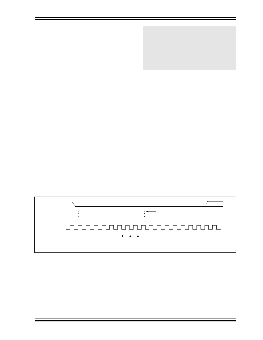
©
1996 Microchip Technology Inc.
DS30412C-page 91
PIC17C4X
13.2.2
USART ASYNCHRONOUS RECEIVER
The receiver block diagram is shown in Figure 13-4.
The data comes in the RA4/RX/DT pin and drives the
data recovery block. The data recovery block is actually
a high speed shifter operating at 16 times the baud
rate, whereas the main receive serial shifter operates
at the bit rate or at F
OSC
.
Once asynchronous mode is selected, reception is
enabled by setting bit CREN (RCSTA<4>).
The heart of the receiver is the receive (serial) shift reg-
ister (RSR). After sampling the stop bit, the received
data in the RSR is transferred to the RCREG (if it is
empty). If the transfer is complete, the interrupt bit
RCIF (PIR<0>) is set. The actual interrupt can be
enabled/disabled by setting/clearing the RCIE
(PIE<0>) bit. RCIF is a read only bit which is cleared by
the hardware. It is cleared when RCREG has been
read and is empty. RCREG is a double buffered regis-
ter; (i.e. it is a two deep FIFO). It is possible for two
bytes of data to be received and transferred to the
RCREG FIFO and a third byte begin shifting to the
RSR. On detection of the stop bit of the third byte, if the
RCREG is still full, then the overrun error bit,
OERR (RCSTA<1>) will be set. The word in the RSR
will be lost. RCREG can be read twice to retrieve the
two bytes in the FIFO. The OERR bit has to be cleared
in software which is done by resetting the receive logic
(CREN is set). If the OERR bit is set, transfers from the
RSR to RCREG are inhibited, so it is essential to clear
the OERR bit if it is set. The framing error bit
FERR (RCSTA<2>) is set if a stop bit is not detected.
13.2.3
SAMPLING
The data on the RA4/RX/DT pin is sampled three times
by a majority detect circuit to determine if a high or a
low level is present at the RA4/RX/DT pin. The sam-
pling is done on the seventh, eighth and ninth falling
edges of a x16 clock (Figure 11-3).
The x16 clock is a free running clock, and the three
sample points occur at a frequency of every 16 falling
edges.
Note:
The FERR and the 9th receive bit are buff-
ered the same way as the receive data.
Reading the RCREG register will allow the
RX9D and FERR bits to be loaded with val-
ues for the next received Received data;
therefore, it is essential for the user to read
the RCSTA register before reading
RCREG in order not to lose the old FERR
and RX9D information.
FIGURE 13-7: RX PIN SAMPLING SCHEME
RX
baud CLK
x16 CLK
Start bit
Bit0
Samples
1 2 3 4 5 6 7 8 9 10 11 12 13 14 15 16 1 2 3
Baud CLK for all but start bit
(RA4/RX/DT pin)

PIC17C4X
DS30412C-page 92
©
1996 Microchip Technology Inc.
Steps to follow when setting up an Asynchronous
Reception:
1.
Initialize the SPBRG register for the appropriate
baud rate.
2.
Enable the asynchronous serial port by clearing
the SYNC bit and setting the SPEN bit.
3.
If interrupts are desired, then set the RCIE bit.
4.
If 9-bit reception is desired, then set the RX9 bit.
5.
Enable the reception by setting the CREN bit.
6.
The RCIF bit will be set when reception com-
pletes and an interrupt will be generated if the
RCIE bit was set.
7.
Read RCSTA to get the ninth bit (if enabled) and
FERR bit to determine if any error occurred dur-
ing reception.
8.
Read RCREG for the 8-bit received data.
9.
If an overrun error occurred, clear the error by
clearing the OERR bit.
Note:
To terminate a reception, either clear the
SREN and CREN bits, or the SPEN bit.
This will reset the receive logic, so that it
will be in the proper state when receive is
re-enabled.
FIGURE 13-8: ASYNCHRONOUS RECEPTION
TABLE 13-6:
REGISTERS ASSOCIATED WITH ASYNCHRONOUS RECEPTION
Address
Name
Bit 7
Bit 6
Bit 5
Bit 4
Bit 3
Bit 2
Bit 1
Bit 0
Value on
Power-on
Reset
Value on all
other resets
(Note1)
16h, Bank 1
PIR
RBIF
TMR3IF
TMR2IF
TMR1IF
CA2IF
CA1IF
TXIF
RCIF
0000 0010
0000 0010
13h, Bank 0
RCSTA
SPEN
RX9
SREN
CREN
--
FERR
OERR
RX9D
0000 -00x
0000 -00u
14h, Bank 0
RCREG
RX7
RX6
RX5
RX4
RX3
RX2
RX1
RX0
xxxx xxxx
uuuu uuuu
17h, Bank 1
PIE
RBIE
TMR3IE
TMR2IE TMR1IE
CA2IE
CA1IE
TXIE
RCIE
0000 0000
0000 0000
15h, Bank 0
TXSTA
CSRC
TX9
TXEN
SYNC
--
--
TRMT
TX9D
0000 --1x
0000 --1u
17h, Bank 0
SPBRG
Baud rate generator register
xxxx xxxx
uuuu uuuu
Legend:
x
= unknown,
u
= unchanged,
-
= unimplemented read as a '0', shaded cells are not used for asynchronous reception.
Note 1:
Other (non power-up) resets include: external reset through MCLR and Watchdog Timer Reset.
Start
bit
bit7/8
bit1
bit0
bit7/8
bit0
Stop
bit
Start
bit
Start
bit
bit7/8
Stop
bit
RX
reg
Rcv buffer reg
Rcv shift
Read Rcv
buffer reg
RCREG
RCIF
(interrupt flag)
OERR bit
CREN
Word 1
RCREG
Word 2
RCREG
Stop
bit
Note: This timing diagram shows three words appearing on the RX input. The RCREG (receive buffer) is read after the third word,
causing the OERR (overrun) bit to be set.
(RA4/RX/DT pin)
Word 3

©
1996 Microchip Technology Inc.
DS30412C-page 93
PIC17C4X
13.3
USART Synchronous Master Mode
In Master Synchronous mode, the data is transmitted in
a half-duplex manner; i.e. transmission and reception
do not occur at the same time: when transmitting data,
the reception is inhibited and vice versa. The synchro-
nous mode is entered by setting the SYNC
(TXSTA<4>) bit. In addition, the SPEN (RCSTA<7>) bit
is set in order to configure the RA5 and RA4 I/O ports
to CK (clock) and DT (data) lines respectively. The
Master mode indicates that the processor transmits the
master clock on the CK line. The Master mode is
entered by setting the CSRC (TXSTA<7>) bit.
13.3.1
USART SYNCHRONOUS MASTER
TRANSMISSION
The USART transmitter block diagram is shown in
Figure 13-3. The heart of the transmitter is the transmit
(serial) shift register (TSR). The shift register obtains its
data from the read/write transmit buffer TXREG.
TXREG is loaded with data in software. The TSR is not
loaded until the last bit has been transmitted from the
previous load. As soon as the last bit is transmitted, the
TSR is loaded with new data from TXREG (if available).
Once TXREG transfers the data to the TSR (occurs in
one T
CY
at the end of the current BRG cycle), TXREG
is empty and the TXIF (PIR<1>) bit is set. This interrupt
can be enabled/disabled by setting/clearing the TXIE
bit (PIE<1>). TXIF will be set regardless of the state of
bit TXIE and cannot be cleared in software. It will reset
only when new data is loaded into TXREG. While TXIF
indicates the status of TXREG, TRMT (TXSTA<1>)
shows the status of the TSR. TRMT is a read only bit
which is set when the TSR is empty. No interrupt logic
is tied to this bit, so the user has to poll this bit in order
to determine if the TSR is empty. The TSR is not
mapped in data memory, so it is not available to the
user.
Transmission is enabled by setting the TXEN
(TXSTA<5>) bit. The actual transmission will not occur
until TXREG has been loaded with data. The first data
bit will be shifted out on the next available rising edge
of the clock on the RA5/TX/CK pin. Data out is stable
around the falling edge of the synchronous clock
(Figure 13-10). The transmission can also be started
by first loading TXREG and then setting TXEN. This is
advantageous when slow baud rates are selected,
since BRG is kept in RESET when the TXEN, CREN,
and SREN bits are clear. Setting the TXEN bit will start
the BRG, creating a shift clock immediately. Normally
when transmission is first started, the TSR is empty, so
a transfer to TXREG will result in an immediate transfer
to the TSR, resulting in an empty TXREG.
Back-to-back transfers are possible.
Clearing TXEN during a transmission will cause the
transmission to be aborted and will reset the transmit-
ter. The RA4/RX/DT and RA5/TX/CK pins will revert to
hi-impedance. If either CREN or SREN are set during
a transmission, the transmission is aborted and the
RA4/RX/DT pin reverts to a hi-impedance state (for a
reception). The RA5/TX/CK pin will remain an output if
the CSRC bit is set (internal clock). The transmitter
logic is not reset, although it is disconnected from the
pins. In order to reset the transmitter, the user has to
clear the TXEN bit. If the SREN bit is set (to interrupt an
ongoing transmission and receive a single word), then
after the single word is received, SREN will be cleared
and the serial port will revert back to transmitting, since
the TXEN bit is still set. The DT line will immediately
switch from hi-impedance receive mode to transmit
and start driving. To avoid this, TXEN should be
cleared.
In order to select 9-bit transmission, the
TX9 (TXSTA<6>) bit should be set and the ninth bit
should be written to TX9D (TXSTA<0>). The ninth bit
must be written before writing the 8-bit data to TXREG.
This is because a data write to TXREG can result in an
immediate transfer of the data to the TSR (if the TSR is
empty). If the TSR was empty and TXREG was written
before writing the "new" TX9D, the "present" value of
TX9D is loaded.
Steps to follow when setting up a Synchronous Master
Transmission:
1.
Initialize the SPBRG register for the appropriate
baud rate (see Baud Rate Generator Section for
details).
2.
Enable the synchronous master serial port by
setting the SYNC, SPEN, and CSRC bits.
3.
Ensure that the CREN and SREN bits are clear
(these bits override transmission when set).
4.
If interrupts are desired, then set the TXIE bit
(the GLINTD bit must be clear and the PEIE bit
must be set).
5.
If 9-bit transmission is desired, then set the TX9
bit.
6.
Start transmission by loading data to the
TXREG register.
7.
If 9-bit transmission is selected, the ninth bit
should be loaded in TX9D.
8.
Enable the transmission by setting TXEN.
Writing the transmit data to the TXREG, then enabling
the transmit (setting TXEN) allows transmission to start
sooner then doing these two events in the reverse
order.
Note:
To terminate a transmission, either clear
the SPEN bit, or the TXEN bit. This will
reset the transmit logic, so that it will be in
the proper state when transmit is
re-enabled.

PIC17C4X
DS30412C-page 94
©
1996 Microchip Technology Inc.
TABLE 13-7:
REGISTERS ASSOCIATED WITH SYNCHRONOUS MASTER TRANSMISSION
FIGURE 13-9: SYNCHRONOUS TRANSMISSION
FIGURE 13-10: SYNCHRONOUS TRANSMISSION (THROUGH TXEN)
Address
Name
Bit 7
Bit 6
Bit 5
Bit 4
Bit 3
Bit 2
Bit 1
Bit 0
Value on
Power-on
Reset
Value on all
other resets
(Note1)
16h, Bank 1
PIR
RBIF
TMR3IF
TMR2IF
TMR1IF
CA2IF
CA1IF
TXIF
RCIF
0000 0010
0000 0010
13h, Bank 0
RCSTA
SPEN
RX9
SREN
CREN
--
FERR
OERR
RX9D
0000 -00x
0000 -00u
16h, Bank 0
TXREG
TX7
TX6
TX5
TX4
TX3
TX2
TX1
TX0
xxxx xxxx
uuuu uuuu
17h, Bank 1
PIE
RBIE
TMR3IE TMR2IE
TMR1IE
CA2IE
CA1IE
TXIE
RCIE
0000 0000
0000 0000
15h, Bank 0
TXSTA
CSRC
TX9
TXEN
SYNC
--
--
TRMT
TX9D
0000 --1x
0000 --1u
17h, Bank 0
SPBRG
Baud rate generator register
xxxx xxxx
uuuu uuuu
Legend:
x
= unknown,
u
= unchanged,
-
= unimplemented read as a '0', shaded cells are not used for synchronous
master transmission.
Note 1:
Other (non power-up) resets include: external reset through MCLR and Watchdog Timer Reset.
Q1 Q2Q3 Q4Q1 Q2Q3 Q4Q1 Q2Q3 Q4Q1 Q2Q3 Q4Q1 Q2Q3 Q4
Q1 Q2Q3 Q4Q1 Q2Q3 Q4Q1 Q2Q3 Q4Q1 Q2Q3 Q4Q1 Q2Q3 Q4Q1 Q2Q3 Q4
Q3 Q4
DT
CK
Write to
TXREG
TXIF
Interrupt flag
TRMT
TXEN
'1'
Note: Sync master mode; BRG = 0. Continuous transmission of two 8-bit words.
Write word 1
Write word 2
bit0
bit1
bit2
bit7
bit0
Word 1
Word 2
(RA4/RX/DT pin)
(RA5/TX/CK pin)
DT
CK
Write to
TXREG
TXIF bit
TRMT bit
bit0
bit1
bit2
bit6
bit7
(RA4/RX/DT pin)
(RA5/TX/CK pin)
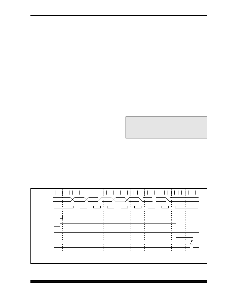
©
1996 Microchip Technology Inc.
DS30412C-page 95
PIC17C4X
13.3.2
USART SYNCHRONOUS MASTER
RECEPTION
Once synchronous mode is selected, reception is
enabled by setting either the SREN (RCSTA<5>) bit or
the CREN (RCSTA<4>) bit. Data is sampled on the
RA4/RX/DT pin on the falling edge of the clock. If
SREN is set, then only a single word is received. If
CREN is set, the reception is continuous until CREN is
reset. If both bits are set, then CREN takes prece-
dence. After clocking the last bit, the received data in
the Receive Shift Register (RSR) is transferred to
RCREG (if it is empty). If the transfer is complete, the
interrupt bit RCIF (PIR<0>) is set. The actual interrupt
can be enabled/disabled by setting/clearing the
RCIE (PIE<0>) bit. RCIF is a read only bit which is
RESET by the hardware. In this case it is reset when
RCREG has been read and is empty. RCREG is a dou-
ble buffered register; i.e., it is a two deep FIFO. It is
possible for two bytes of data to be received and trans-
ferred to the RCREG FIFO and a third byte to begin
shifting into the RSR. On the clocking of the last bit of
the third byte, if RCREG is still full, then the overrun
error bit OERR (RCSTA<1>) is set. The word in the
RSR will be lost. RCREG can be read twice to retrieve
the two bytes in the FIFO. The OERR bit has to be
cleared in software. This is done by clearing the CREN
bit. If OERR bit is set, transfers from RSR to RCREG
are inhibited, so it is essential to clear OERR bit if it is
set. The 9th receive bit is buffered the same way as the
receive data. Reading the RCREG register will allow
the RX9D and FERR bits to be loaded with values for
the next received data; therefore, it is essential for the
user to read the RCSTA register before reading
RCREG in order not to lose the old FERR and RX9D
information.
Steps to follow when setting up a Synchronous Master
Reception:
1.
Initialize the SPBRG register for the appropriate
baud rate. See Section 13.1 for details.
2.
Enable the synchronous master serial port by
setting bits SYNC, SPEN, and CSRC.
3.
If interrupts are desired, then set the RCIE bit.
4.
If 9-bit reception is desired, then set the RX9 bit.
5.
If a single reception is required, set bit SREN.
For continuous reception set bit CREN.
6.
The RCIF bit will be set when reception is com-
plete and an interrupt will be generated if the
RCIE bit was set.
7.
Read RCSTA to get the ninth bit (if enabled) and
determine if any error occurred during reception.
8.
Read the 8-bit received data by reading
RCREG.
9.
If any error occurred, clear the error by clearing
CREN.
Note:
To terminate a reception, either clear the
SREN and CREN bits, or the SPEN bit.
This will reset the receive logic, so that it
will be in the proper state when receive is
re-enabled.
FIGURE 13-11: SYNCHRONOUS RECEPTION (MASTER MODE, SREN)
CREN bit
DT
CK
Write to the
SREN bit
SREN bit
RCIF bit
Read
RCREG
Note: Timing diagram demonstrates SYNC master mode with SREN = 1.
Q3 Q4 Q1 Q2 Q3 Q4 Q1 Q2 Q3 Q4
Q2
Q1 Q2 Q3 Q4Q1 Q2 Q3 Q4 Q1 Q2 Q3 Q4Q1 Q2 Q3 Q4 Q1 Q2 Q3 Q4Q1 Q2 Q3 Q4 Q1 Q2 Q3 Q4
'0'
bit0
bit1
bit2
bit3
bit4
bit5
bit6
bit7
'0'
Q1 Q2 Q3 Q4
(RA4/RX/DT pin)
(RA5/TX/CK pin)

PIC17C4X
DS30412C-page 96
©
1996 Microchip Technology Inc.
TABLE 13-8:
REGISTERS ASSOCIATED WITH SYNCHRONOUS MASTER RECEPTION
Address
Name
Bit 7
Bit 6
Bit 5
Bit 4
Bit 3
Bit 2
Bit 1
Bit 0
Value on
Power-on
Reset
Value on all
other resets
(Note1)
16h, Bank 1
PIR
RBIF
TMR3IF
TMR2IF
TMR1IF
CA2IF
CA1IF
TXIF
RCIF
0000 0010
0000 0010
13h, Bank 0
RCSTA
SPEN
RX9
SREN
CREN
--
FERR
OERR
RX9D
0000 -00x
0000 -00u
14h, Bank 0
RCREG
RX7
RX6
RX5
RX4
RX3
RX2
RX1
RX0
xxxx xxxx
uuuu uuuu
17h, Bank 1
PIE
RBIE
TMR3IE
TMR2IE TMR1IE
CA2IE
CA1IE
TXIE
RCIE
0000 0000
0000 0000
15h, Bank 0
TXSTA
CSRC
TX9
TXEN
SYNC
--
--
TRMT
TX9D
0000 --1x
0000 --1u
17h, Bank 0
SPBRG
Baud rate generator register
xxxx xxxx
uuuu uuuu
Legend:
x
= unknown,
u
= unchanged,
-
= unimplemented read as a '0', shaded cells are not used for synchronous
master reception.
Note 1:
Other (non power-up) resets include: external reset through MCLR and Watchdog Timer Reset.

©
1996 Microchip Technology Inc.
DS30412C-page 97
PIC17C4X
13.4
USART Synchronous Slave Mode
The synchronous slave mode differs from the master
mode in the fact that the shift clock is supplied exter-
nally at the RA5/TX/CK pin (instead of being supplied
internally in the master mode). This allows the device
to transfer or receive data in the SLEEP mode. The
slave mode is entered by clearing the
CSRC (TXSTA<7>) bit.
13.4.1
USART SYNCHRONOUS SLAVE
TRANSMIT
The operation of the sync master and slave modes are
identical except in the case of the SLEEP mode.
If two words are written to TXREG and then the
SLEEP
instruction executes, the following will occur. The first
word will immediately transfer to the TSR and will trans-
mit as the shift clock is supplied. The second word will
remain in TXREG. TXIF will not be set. When the first
word has been shifted out of TSR, TXREG will transfer
the second word to the TSR and the TXIF flag will now
be set. If TXIE is enabled, the interrupt will wake the
chip from SLEEP and if the global interrupt is enabled,
then the program will branch to interrupt vector
(0020h).
Steps to follow when setting up a Synchronous Slave
Transmission:
1.
Enable the synchronous slave serial port by set-
ting the SYNC and SPEN bits and clearing the
CSRC bit.
2.
Clear the CREN bit.
3.
If interrupts are desired, then set the TXIE bit.
4.
If 9-bit transmission is desired, then set the TX9
bit.
5.
Start transmission by loading data to TXREG.
6.
If 9-bit transmission is selected, the ninth bit
should be loaded in TX9D.
7.
Enable the transmission by setting TXEN.
Writing the transmit data to the TXREG, then enabling
the transmit (setting TXEN) allows transmission to start
sooner then doing these two events in the reverse
order.
Note:
To terminate a transmission, either clear
the SPEN bit, or the TXEN bit. This will
reset the transmit logic, so that it will be in
the proper state when transmit is
re-enabled.
13.4.2
USART SYNCHRONOUS SLAVE
RECEPTION
Operation of the synchronous master and slave modes
are identical except in the case of the SLEEP mode.
Also, SREN is a don't care in slave mode.
If receive is enabled (CREN) prior to the
SLEEP
instruc-
tion, then a word may be received during SLEEP. On
completely receiving the word, the RSR will transfer the
data to RCREG (setting RCIF) and if the RCIE bit is set,
the interrupt generated will wake the chip from SLEEP.
If the global interrupt is enabled, the program will
branch to the interrupt vector (0020h).
Steps to follow when setting up a Synchronous Slave
Reception:
1.
Enable the synchronous master serial port by
setting the SYNC and SPEN bits and clearing
the CSRC bit.
2.
If interrupts are desired, then set the RCIE bit.
3.
If 9-bit reception is desired, then set the RX9 bit.
4.
To enable reception, set the CREN bit.
5.
The RCIF bit will be set when reception is com-
plete and an interrupt will be generated if the
RCIE bit was set.
6.
Read RCSTA to get the ninth bit (if enabled) and
determine if any error occurred during reception.
7.
Read the 8-bit received data by reading
RCREG.
8.
If any error occurred, clear the error by clearing
the CREN bit.
Note:
To abort reception, either clear the SPEN
bit, the SREN bit (when in single receive
mode), or the CREN bit (when in continu-
ous receive mode). This will reset the
receive logic, so that it will be in the proper
state when receive is re-enabled.

PIC17C4X
DS30412C-page 98
©
1996 Microchip Technology Inc.
TABLE 13-9:
REGISTERS ASSOCIATED WITH SYNCHRONOUS SLAVE TRANSMISSION
TABLE 13-10: REGISTERS ASSOCIATED WITH SYNCHRONOUS SLAVE RECEPTION
Address
Name
Bit 7
Bit 6
Bit 5
Bit 4
Bit 3
Bit 2
Bit 1
Bit 0
Value on
Power-on
Reset
Value on all
other resets
(Note1)
16h, Bank 1
PIR
RBIF
TMR3IF
TMR2IF
TMR1IF
CA2IF
CA1IF
TXIF
RCIF
0000 0010
0000 0010
13h, Bank 0
RCSTA
SPEN
RX9
SREN
CREN
--
FERR
OERR
RX9D
0000 -00x
0000 -00u
16h, Bank 0
TXREG
TX7
TX6
TX5
TX4
TX3
TX2
TX1
TX0
xxxx xxxx
uuuu uuuu
17h, Bank 1
PIE
RBIE
TMR3IE TMR2IE
TMR1IE
CA2IE
CA1IE
TXIE
RCIE
0000 0000
0000 0000
15h, Bank 0
TXSTA
CSRC
TX9
TXEN
SYNC
--
--
TRMT
TX9D
0000 --1x
0000 --1u
17h, Bank 0
SPBRG
Baud rate generator register
xxxx xxxx
uuuu uuuu
Legend:
x
= unknown,
u
= unchanged,
-
= unimplemented read as a '0', shaded cells are not used for synchronous
slave transmission.
Note 1:
Other (non power-up) resets include: external reset through MCLR and Watchdog Timer Reset.
Address
Name
Bit 7
Bit 6
Bit 5
Bit 4
Bit 3
Bit 2
Bit 1
Bit 0
Value on
Power-on
Reset
Value on all
other resets
(Note1)
16h, Bank1
PIR
RBIF
TMR3IF
TMR2IF
TMR1IF
CA2IF
CA1IF
TXIF
RCIF
0000 0010
0000 0010
13h, Bank0
RCSTA
SPEN
RX9
SREN
CREN
--
FERR
OERR
RX9D
0000 -00x
0000 -00u
14h, Bank0
RCREG
RX7
RX6
RX5
RX4
RX3
RX2
RX1
RX0
xxxx xxxx
uuuu uuuu
17h, Bank1
PIE
RBIE
TMR3IE
TMR2IE TMR1IE
CA2IE
CA1IE
TXIE
RCIE
0000 0000
0000 0000
15h, Bank 0
TXSTA
CSRC
TX9
TXEN
SYNC
--
--
TRMT
TX9D
0000 --1x
0000 --1u
17h, Bank0
SPBRG
Baud rate generator register
xxxx xxxx
uuuu uuuu
Legend:
x
= unknown,
u
= unchanged,
-
= unimplemented read as a '0', shaded cells are not used for synchronous
slave reception.
Note 1:
Other (non power-up) resets include: external reset through MCLR and Watchdog Timer Reset.

©
1996 Microchip Technology Inc.
DS30412C-page 99
PIC17C4X
14.0
SPECIAL FEATURES OF THE
CPU
What sets a microcontroller apart from other proces-
sors are special circuits to deal with the needs of real
time applications. The PIC17CXX family has a host of
such features intended to maximize system reliability,
minimize cost through elimination of external compo-
nents, provide power saving operating modes and offer
code protection. These are:
∑ OSC selection
∑ Reset
- Power-on Reset (POR)
- Power-up Timer (PWRT)
- Oscillator Start-up Timer (OST)
∑ Interrupts
∑ Watchdog Timer (WDT)
∑ SLEEP
∑ Code protection
The PIC17CXX has a Watchdog Timer which can be
shut off only through EPROM bits. It runs off its own RC
oscillator for added reliability. There are two timers that
offer necessary delays on power-up. One is the Oscil-
lator Start-up Timer (OST), intended to keep the chip in
RESET until the crystal oscillator is stable. The other is
the Power-up Timer (PWRT), which provides a fixed
delay of 96 ms (nominal) on power-up only, designed to
keep the part in RESET while the power supply stabi-
lizes. With these two timers on-chip, most applications
need no external reset circuitry.
The SLEEP mode is designed to offer a very low cur-
rent power-down mode. The user can wake from
SLEEP through external reset, Watchdog Timer Reset
or through an interrupt. Several oscillator options are
also made available to allow the part to fit the applica-
tion. The RC oscillator option saves system cost while
the LF crystal option saves power. Configuration bits
are used to select various options. This configuration
word has the format shown in Figure 14-1.
FIGURE 14-1: CONFIGURATION WORD
R/P - 1
U - x
U - x
U - x
U - x
U - x
U - x
U - x
PM2
(1)
--
--
--
--
--
--
--
bit15-7
bit0
U - x
R/P - 1
U - x
R/P - 1
R/P - 1
R/P - 1
R/P - 1
R/P - 1
--
PM1
--
PM0
WDTPS1 WDTPS0
FOSC1
FOSC0
R = Readable bit
P = Programmable bit
U = Unimplemented
- n = Value for Erased Device
(x = unknown)
bit15-7
bit0
bit 15-9:
Unimplemented
: Read as a '1'
bit 15,6,4:
PM2, PM1, PM0
, Processor Mode Select bits
111 = Microprocessor Mode
110 = Microcontroller mode
101 = Extended microcontroller mode
000 = Code protected microcontroller mode
bit 7, 5:
Unimplemented
: Read as a '0'
bit 3-2:
WDTPS1:WDTPS0
, WDT Postscaler Select bits
11 = WDT enabled, postscaler = 1
10 = WDT enabled, postscaler = 256
01 = WDT enabled, postscaler = 64
00 = WDT disabled, 16-bit overflow timer
bit 1-0:
FOSC1:FOSC0
, Oscillator Select bits
11 = EC oscillator
10 = XT oscillator
01 = RC oscillator
00 = LF oscillator
Note 1: This bit does not exist on the PIC17C42. Reading this bit will return an unknown value (x).
This document was created with FrameMaker 4 0 4

PIC17C4X
DS30412C-page 100
©
1996 Microchip Technology Inc.
14.1
Configuration Bits
The PIC17CXX has up to seven configuration locations
(Table 14-1). These locations can be programmed
(read as '0') or left unprogrammed (read as '1') to select
various device configurations. Any write to a configura-
tion location, regardless of the data, will program that
configuration bit. A
TABLWT
instruction is required to
write to program memory locations. The configuration
bits can be read by using the
TABLRD
instructions.
Reading any configuration location between FE00h
and FE07h will read the low byte of the configuration
word (Figure 14-1) into the TABLATL register. The TAB-
LATH register will be FFh. Reading a configuration
location between FE08h and FE0Fh will read the high
byte of the configuration word into the TABLATL regis-
ter. The TABLATH register will be FFh.
Addresses FE00h thorough FE0Fh are only in the pro-
gram memory space for microcontroller and code pro-
tected microcontroller modes. A device programmer
will be able to read the configuration word in any pro-
cessor mode. See programming specifications for more
detail.
TABLE 14-1:
CONFIGURATION
LOCATIONS
Bit
Address
FOSC0
FE00h
FOSC1
FE01h
WDTPS0
FE02h
WDTPS1
FE03h
PM0
FE04h
PM1
FE06h
PM2
(1)
FE0Fh
(1)
Note 1: This location does not exist on the
PIC17C42.
Note:
When programming the desired configura-
tion locations, they must be programmed in
ascending order. Starting with address
FE00h.
14.2
Oscillator Configurations
14.2.1
OSCILLATOR TYPES
The PIC17CXX can be operated in four different oscil-
lator modes. The user can program two configuration
bits (FOSC1:FOSC0) to select one of these four
modes:
∑ LF:
Low Power Crystal
∑ XT:
Crystal/Resonator
∑ EC:
External Clock Input
∑ RC:
Resistor/Capacitor
14.2.2
CRYSTAL OSCILLATOR / CERAMIC
RESONATORS
In XT or LF modes, a crystal or ceramic resonator is
connected to the OSC1/CLKIN and OSC2/CLKOUT
pins to establish oscillation (Figure
14-2). The
PIC17CXX Oscillator design requires the use of a par-
allel cut crystal. Use of a series cut crystal may give a
frequency out of the crystal manufacturers specifica-
tions.
For frequencies above 20 MHz, it is common for the
crystal to be an overtone mode crystal. Use of overtone
mode crystals require a tank circuit to attenuate the
gain at the fundamental frequency. Figure 14-3 shows
an example of this.
FIGURE 14-2: CRYSTAL OR CERAMIC
RESONATOR OPERATION
(XT OR LF OSC
CONFIGURATION)
See Table 14-2 and Table 14-3 for recommended
values of C1 and C2.
Note 1:
A series resistor may be required for AT strip
cut crystals.
C1
C2
XTAL
OSC2
Note1
OSC1
RF
SLEEP
PIC17CXX
To internal
logic

©
1996 Microchip Technology Inc.
DS30412C-page 101
PIC17C4X
FIGURE 14-3: CRYSTAL OPERATION,
OVERTONE CRYSTALS (XT
OSC CONFIGURATION)
TABLE 14-2:
CAPACITOR SELECTION
FOR CERAMIC
RESONATORS
Oscillator
Type
Resonator
Frequency
Capacitor Range
C1 = C2
LF
455 kHz
2.0 MHz
15 - 68 pF
10 - 33 pF
XT
4.0 MHz
8.0 MHz
16.0 MHz
22 - 68 pF
33 - 100 pF
33 - 100 pF
Higher capacitance increases the stability of the
oscillator but also increases the start-up time. These
values are for design guidance only. Since each reso-
nator has its own characteristics, the user should
consult the resonator manufacturer for appropriate
values of external components.
Resonators Used:
455 kHz
Panasonic EFO-A455K04B
±
0.3%
2.0 MHz
Murata Erie CSA2.00MG
±
0.5%
4.0 MHz
Murata Erie CSA4.00MG
±
0.5%
8.0 MHz
Murata Erie CSA8.00MT
±
0.5%
16.0 MHz
Murata Erie CSA16.00MX
±
0.5%
Resonators used did not have built-in capacitors.
C1
C2
0.1
µ
F
SLEEP
OSC2
OSC1
PIC17C42
To filter the fundamental frequency
1
LC2
= (2
f)
2
Where f = tank circuit resonant frequency. This should be
midway between the fundamental and the 3rd overtone
frequencies of the crystal.
TABLE 14-3:
CAPACITOR SELECTION
FOR CRYSTAL OSCILLATOR
14.2.3
EXTERNAL CLOCK OSCILLATOR
In the EC oscillator mode, the OSC1 input can be
driven by CMOS drivers. In this mode, the
OSC1/CLKIN pin is hi-impedance and the OSC2/CLK-
OUT pin is the CLKOUT output (4 T
OSC
).
FIGURE 14-4: EXTERNAL CLOCK INPUT
OPERATION (EC OSC
CONFIGURATION)
Osc
Type
Freq
C1
C2
LF
32 kHz
(1)
1 MHz
2 MHz
100-150 pF
10-33 pF
10-33 pF
100-150 pF
10-33 pF
10-33 pF
XT
2 MHz
4 MHz
8 MHz
(2)
16 MHz
25 MHz
32 MHz
(3)
47-100 pF
15-68 pF
15-47 pF
TBD
15-47 pF
0
(3)
47-100 pF
15-68 pF
15-47 pF
TBD
15-47 pF
0
(3)
Higher capacitance increases the stability of the
oscillator but also increases the start-up time and the
oscillator current. These values are for design guid-
ance only. R
S
may be required in XT mode to avoid
overdriving the crystals with low drive level specifica-
tion. Since each crystal has its own characteristics,
the user should consult the crystal manufacturer for
appropriate values for external components.
Note 1: For V
DD
> 4.5V, C1 = C2
30 pF is recom-
mended.
2: R
S
of 330
is required for a capacitor com-
bination of 15/15 pF.
3:
Only the capacitance of the board was present.
Crystals Used:
32.768 kHz
Epson C-001R32.768K-A
±
20 PPM
1.0 MHz
ECS-10-13-1
±
50 PPM
2.0 MHz
ECS-20-20-1
±
50 PPM
4.0 MHz
ECS-40-20-1
±
50 PPM
8.0 MHz
ECS ECS-80-S-4
ECS-80-18-1
±
50 PPM
16.0 MHz
ECS-160-20-1
TBD
25 MHz
CTS CTS25M
±
50 PPM
32 MHz
CRYSTEK HF-2
±
50 PPM
Clock from
ext. system
OSC1
OSC2
PIC17CXX
CLKOUT
(F
OSC
/4)
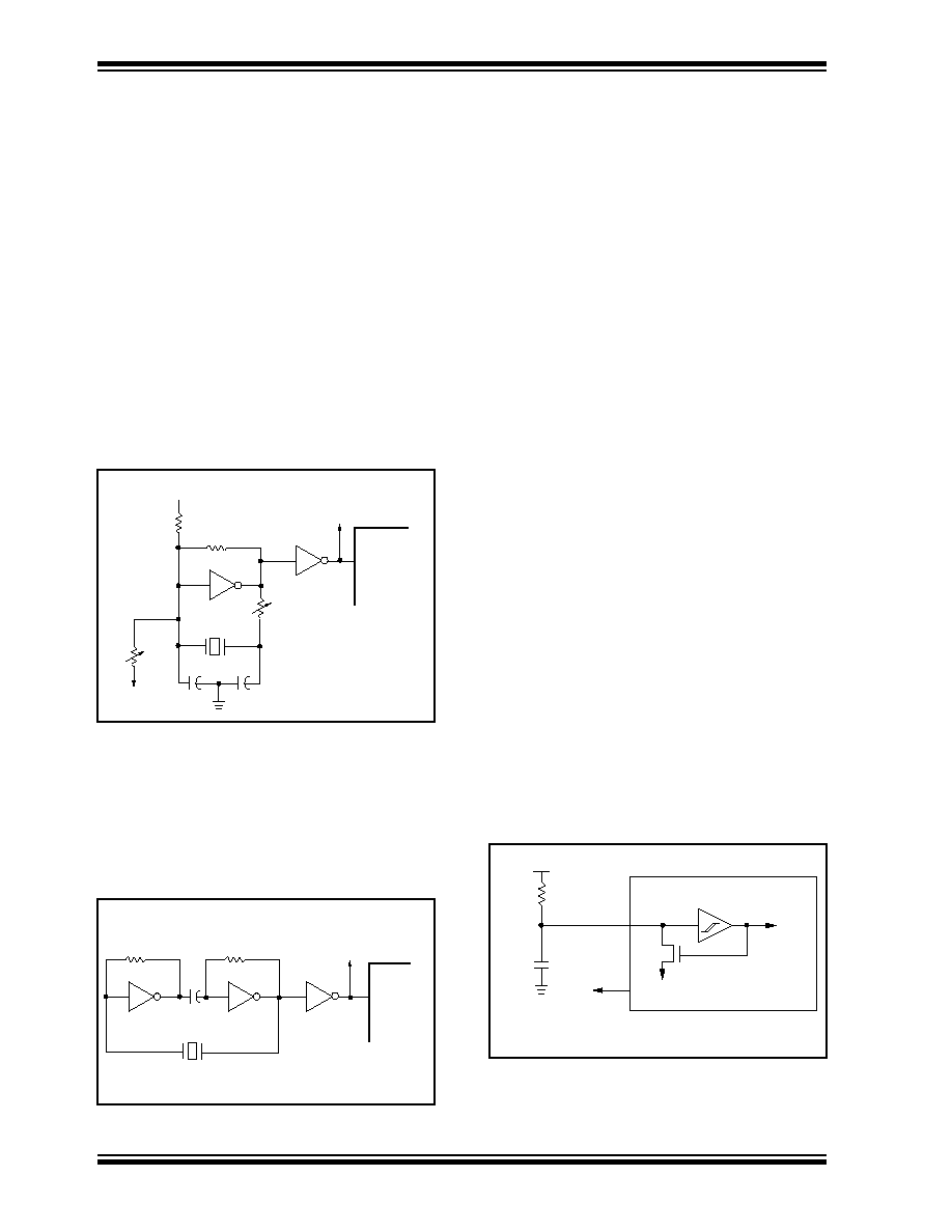
PIC17C4X
DS30412C-page 102
©
1996 Microchip Technology Inc.
14.2.4
EXTERNAL CRYSTAL OSCILLATOR
CIRCUIT
Either a prepackaged oscillator can be used or a simple
oscillator circuit with TTL gates can be built. Prepack-
aged oscillators provide a wide operating range and
better stability. A well-designed crystal oscillator will
provide good performance with TTL gates. Two types of
crystal oscillator circuits can be used: one with series
resonance, or one with parallel resonance.
Figure 14-5 shows implementation of a parallel reso-
nant oscillator circuit. The circuit is designed to use the
fundamental frequency of the crystal. The 74AS04
inverter performs the 180-degree phase shift that a par-
allel oscillator requires. The 4.7 k
resistor provides the
negative feedback for stability. The 10 k
potentiometer
biases the 74AS04 in the linear region. This could be
used for external oscillator designs.
FIGURE 14-5: EXTERNAL PARALLEL
RESONANT CRYSTAL
OSCILLATOR CIRCUIT
Figure 14-6 shows a series resonant oscillator circuit.
This circuit is also designed to use the fundamental fre-
quency of the crystal. The inverter performs a
180-degree phase shift in a series resonant oscillator
circuit. The 330 k
resistors provide the negative feed-
back to bias the inverters in their linear region.
FIGURE 14-6: EXTERNAL SERIES
RESONANT CRYSTAL
OSCILLATOR CIRCUIT
20 pF
+5V
20 pF
10k
4.7k
10k
74AS04
XTAL
10k
74AS04
PIC17CXX
OSC1
To Other
Devices
330 k
74AS04
74AS04
PIC17CXX
OSC1
To Other
Devices
XTAL
330 k
74AS04
0.1
µ
F
14.2.5
RC OSCILLATOR
For timing insensitive applications, the RC device
option offers additional cost savings. RC oscillator fre-
quency is a function of the supply voltage, the resistor
(Rext) and capacitor (Cext) values, and the operating
temperature. In addition to this, oscillator frequency will
vary from unit to unit due to normal process parameter
variation. Furthermore, the difference in lead frame
capacitance between package types will also affect
oscillation frequency, especially for low Cext values.
The user also needs to take into account variation due
to tolerance of external R and C components used.
Figure 14-6 shows how the R/C combination is con-
nected to the PIC17CXX. For Rext values below 2.2 k
,
the oscillator operation may become unstable, or stop
completely. For very high Rext values (e.g. 1 M
), the
oscillator becomes sensitive to noise, humidity and
leakage. Thus, we recommend to keep Rext between 3
k
and 100 k
.
Although the oscillator will operate with no external
capacitor (Cext = 0 pF), we recommend using values
above 20 pF for noise and stability reasons. With little
or no external capacitance, oscillation frequency can
vary dramatically due to changes in external capaci-
tances, such as PCB trace capacitance or package
lead frame capacitance.
See Section 18.0 for RC frequency variation from part
to part due to normal process variation. The variation
is larger for larger R (since leakage current variation will
affect RC frequency more for large R) and for smaller C
(since variation of input capacitance will affect RC fre-
quency more).
See Section 18.0 for variation of oscillator frequency
due to V
DD
for given Rext/Cext values as well as fre-
quency variation due to operating temperature for given
R, C, and V
DD
values.
The oscillator frequency, divided by 4, is available on
the OSC2/CLKOUT pin, and can be used for test pur-
poses or to synchronize other logic (see Figure 3-2 for
waveform).
FIGURE 14-7: RC OSCILLATOR MODE
V
DD
Rext
Cext
V
SS
OSC1
Internal
clock
OSC2/CLKOUT
Fosc/4
PIC17CXX

©
1996 Microchip Technology Inc.
DS30412C-page 103
PIC17C4X
14.3
Watchdog Timer (WDT)
The Watchdog Timer's function is to recover from soft-
ware malfunction. The WDT uses an internal free run-
ning on-chip RC oscillator for its clock source. This
does not require any external components. This RC
oscillator is separate from the RC oscillator of the
OSC1/CLKIN pin. That means that the WDT will run,
even if the clock on the OSC1/CLKIN and OSC2/CLK-
OUT pins of the device has been stopped, for example,
by execution of a
SLEEP
instruction. During normal
operation and SLEEP mode, a WDT time-out gener-
ates a device RESET. The WDT can be permanently
disabled by programming the configuration bits
WDTPS1:WDTPS0 as '
00
' (Section 14.1).
Under normal operation, the WDT must be cleared on
a regular interval. This time is less the minimum WDT
overflow time. Not clearing the WDT in this time frame
will cause the WDT to overflow and reset the device.
14.3.1
WDT PERIOD
The WDT has a nominal time-out period of 12 ms, (with
postscaler = 1). The time-out periods vary with temper-
ature, V
DD
and process variations from part to part (see
DC specs). If longer time-out periods are desired, a
postscaler with a division ratio of up to 1:256 can be
assigned to the WDT. Thus, typical time-out periods up
to 3.0 seconds can be realized.
The
CLRWDT
and
SLEEP
instructions clear the WDT
and the postscaler (if assigned to the WDT) and pre-
vent it from timing out thus generating a device RESET
condition.
The TO bit in the CPUSTA register will be cleared upon
a WDT time-out.
14.3.2
CLEARING THE WDT AND POSTSCALER
The WDT and postscaler are cleared when:
∑ The device is in the reset state
∑ A
SLEEP
instruction is executed
∑ A
CLRWDT
instruction is executed
∑ Wake-up from SLEEP by an interrupt
The WDT counter/postscaler will start counting on the
first edge after the device exits the reset state.
14.3.3
WDT PROGRAMMING CONSIDERATIONS
It should also be taken in account that under worst case
conditions (V
DD
= Min., Temperature = Max., max.
WDT postscaler) it may take several seconds before a
WDT time-out occurs.
The WDT and postscaler is the Power-up Timer during
the Power-on Reset sequence.
14.3.4
WDT AS NORMAL TIMER
When the WDT is selected as a normal timer, the clock
source is the device clock. Neither the WDT nor the
postscaler are directly readable or writable. The over-
flow time is 65536 T
OSC
cycles. On overflow, the TO bit
is cleared (device is not reset). The
CLRWDT
instruction
can be used to set the TO bit. This allows the WDT to
be a simple overflow timer. When in sleep, the WDT
does not increment.

PIC17C4X
DS30412C-page 104
©
1996 Microchip Technology Inc.
FIGURE 14-8: WATCHDOG TIMER BLOCK DIAGRAM
TABLE 14-4:
REGISTERS/BITS ASSOCIATED WITH THE WATCHDOG TIMER
Address
Name
Bit 7
Bit 6
Bit 5
Bit 4
Bit 3
Bit 2
Bit 1
Bit 0
Value on
Power-on
Reset
Value on all
other resets
(Note1)
--
Config
--
PM1
--
PM0
WDTPS1
WDTPS0
FOSC1
FOSC0
(Note 2)
(Note 2)
06h, Unbanked
CPUSTA
--
--
STKAV
GLINTD
TO
PD
--
--
--11 11--
--11 qq--
Legend:
-
= unimplemented read as '0',
q
- value depends on condition, shaded cells are not used by the WDT.
Note 1:
Other (non power-up) resets include: external reset through MCLR and Watchdog Timer Reset.
2:
This value will be as the device was programmed, or if unprogrammed, will read as all '1's.
WDT
WDT Enable
Postscaler
4 - to - 1 MUX
WDTPS1:WDTPS0
On-chip RC
WDT Overflow
Oscillator
(1)
Note 1: This oscillator is separate from the external
RC oscillator on the OSC1 pin.

©
1996 Microchip Technology Inc.
DS30412C-page 105
PIC17C4X
14.4
Power-down Mode (SLEEP)
The Power-down mode is entered by executing a
SLEEP
instruction. This clears the Watchdog Timer and
postscaler (if enabled). The PD bit is cleared and the
TO bit is set (in the CPUSTA register). In SLEEP mode,
the oscillator driver is turned off. The I/O ports maintain
their status (driving high, low, or hi-impedance).
The MCLR/V
PP
pin must be at a logic high level
(V
IHMC
). A WDT time-out RESET does not drive the
MCLR/V
PP
pin low.
14.4.1
WAKE-UP FROM SLEEP
The device can wake up from SLEEP through one of
the following events:
∑ A POR reset
∑ External reset input on MCLR/V
PP
pin
∑ WDT Reset (if WDT was enabled)
∑ Interrupt from RA0/INT pin, RB port change,
T0CKI interrupt, or some Peripheral Interrupts
The following peripheral interrupts can wake-up from
SLEEP:
∑ Capture1 interrupt
∑ Capture2 interrupt
∑ USART synchronous slave transmit interrupt
∑ USART synchronous slave receive interrupt
Other peripherals can not generate interrupts since
during SLEEP, no on-chip Q clocks are present.
Any reset event will cause a device reset. Any interrupt
event is considered a continuation of program execu-
tion. The TO and PD bits in the CPUSTA register can
be used to determine the cause of device reset. The
PD bit, which is set on power-up, is cleared when
SLEEP is invoked. The TO bit is cleared if WDT
time-out occurred (and caused wake-up).
When the
SLEEP
instruction is being executed, the next
instruction (PC + 1) is pre-fetched. For the device to
wake-up through an interrupt event, the corresponding
interrupt enable bit must be set (enabled). Wake-up is
regardless of the state of the GLINTD bit. If the GLINTD
bit is set (disabled), the device continues execution at
the instruction after the
SLEEP
instruction. If the
GLINTD bit is clear (enabled), the device executes the
instruction after the
SLEEP
instruction and then
branches to the interrupt vector address. In cases
where the execution of the instruction following SLEEP
is not desirable, the user should have a NOP after the
SLEEP
instruction.
The WDT is cleared when the device wake from
SLEEP, regardless of the source of wake-up.
14.4.1.1
WAKE-UP DELAY
When the oscillator type is configured in XT or LF
mode, the Oscillator Start-up Timer (OST) is activated
on wake-up. The OST will keep the device in reset for
1024T
OSC
. This needs to be taken into account when
considering the interrupt response time when coming
out of SLEEP.
Note:
If the global interrupts are disabled
(GLINTD is set), but any interrupt source
has both its interrupt enable bit and the cor-
responding interrupt flag bits set, the
device will immediately wake-up from
sleep. The TO bit is set, and the PD bit is
cleared.
FIGURE 14-9: WAKE-UP FROM SLEEP THROUGH INTERRUPT
Q2
Q1
Q3
Q4
Q2
Q1
Q3
Q4
Q2
Q1
Q3
Q4
Q2
Q1
Q3
Q4
Q2
Q1
Q3
Q4
OSC1
CLKOUT(4)
INT
INTF flag
GLINTD bit
INSTRUCTION FLOW
PC
Instruction
fetched
Instruction
executed
Interrupt Latency (2)
PC
PC+1
PC+2
0004h
0005h
Dummy Cycle
Inst (PC) = SLEEP
Inst (PC+1)
Inst (PC-1)
SLEEP
Tost(2)
Processor
in SLEEP
Inst (PC+2)
Inst (PC+1)
Note 1: XT or LF oscillator mode assumed.
2: Tost = 1024Tosc (drawing not to scale). This delay will not be there for RC osc mode.
3: When GLINTD = 0 processor jumps to interrupt routine after wake-up. If GLINTD = 1, execution will continue in line.
4: CLKOUT is not available in these osc modes, but shown here for timing reference.
(RA0/INT pin)

PIC17C4X
DS30412C-page 106
©
1996 Microchip Technology Inc.
14.4.2
MINIMIZING CURRENT CONSUMPTION
To minimize current consumption, all I/O pins should be
either at V
DD
, or V
SS
, with no external circuitry drawing
current from the I/O pin. I/O pins that are hi-impedance
inputs should be pulled high or low externally to avoid
switching currents caused by floating inputs. The
T0CKI input should be at V
DD
or V
SS
. The contributions
from on-chip pull-ups on PORTB should also be con-
sidered, and disabled when possible.
14.5
Code Protection
The code in the program memory can be protected by
selecting the microcontroller in code protected mode
(PM2:PM0 = '
000
').
In this mode, instructions that are in the on-chip pro-
gram memory space, can continue to read or write the
program memory. An instruction that is executed out-
side of the internal program memory range will be inhib-
ited from writing to or reading from program memory.
If the code protection bit(s) have not been pro-
grammed, the on-chip program memory can be read
out for verification purposes.
Note:
PM2 does not exist on the PIC17C42. To
select code protected microcontroller
mode, PM1:PM0 = '
00
'.
Note:
Microchip does not recommend code pro-
tecting windowed devices.

©
1996 Microchip Technology Inc.
DS30412C-page 107
PIC17C4X
15.0
INSTRUCTION SET SUMMARY
The PIC17CXX instruction set consists of 58 instruc-
tions. Each instruction is a 16-bit word divided into an
OPCODE and one or more operands. The opcode
specifies the instruction type, while the operand(s) fur-
ther specify the operation of the instruction. The
PIC17CXX instruction set can be grouped into three
types:
∑ byte-oriented
∑ bit-oriented
∑ literal and control operations.
These formats are shown in Figure 15-1.
Table
15-1 shows the field descriptions for the
opcodes. These descriptions are useful for under-
standing the opcodes in Table 15-2 and in each spe-
cific instruction descriptions.
byte-oriented instructions
, 'f' represents a file regis-
ter designator and 'd' represents a destination designa-
tor. The file register designator specifies which file
register is to be used by the instruction.
The destination designator specifies where the result of
the operation is to be placed. If 'd' = '0', the result is
placed in the WREG register. If 'd' = '1', the result is
placed in the file register specified by the instruction.
bit-oriented instructions
, 'b' represents a bit field des-
ignator which selects the number of the bit affected by
the operation, while 'f' represents the number of the file
in which the bit is located.
literal and control operations
, 'k' represents an 8- or
11-bit constant or literal value.
The instruction set is highly orthogonal and is grouped
into:
∑ byte-oriented operations
∑ bit-oriented operations
∑ literal and control operations
All instructions are executed within one single instruc-
tion cycle, unless:
∑ a conditional test is true
∑ the program counter is changed as a result of an
instruction
∑ a table read or a table write instruction is exe-
cuted (in this case, the execution takes two
instruction cycles with the second cycle executed
as a NOP
)
One instruction cycle consists of four oscillator periods.
Thus, for an oscillator frequency of 25 MHz, the normal
instruction execution time is 160 ns. If a conditional test
is true or the program counter is changed as a result of
an instruction, the instruction execution time is 320 ns.
TABLE 15-1:
OPCODE FIELD
DESCRIPTIONS
Field
Description
f
Register file address (00h to FFh)
p
Peripheral register file address (00h to 1Fh)
i
Table pointer control i = '0' (do not change)
i = '1' (increment after instruction execution)
t
Table byte select t = '0' (perform operation on lower
byte)
t = '1' (perform operation on upper byte literal field,
constant data)
WREG
Working register (accumulator)
b
Bit address within an 8-bit file register
k
Literal field, constant data or label
x
Don't care location (= '0' or '1')
The assembler will generate code with x = '0'. It is
the recommended form of use for compatibility with
all Microchip software tools.
d
Destination select
0 = store result in WREG
1 = store result in file register f
Default is d = '1'
u
Unused, encoded as '0'
s
Destination select
0 = store result in file register f and in the WREG
1 = store result in file register f
Default is s = '1'
label
Label name
C,DC,
Z,OV
ALU status bits Carry, Digit Carry, Zero, Overflow
GLINTD
Global Interrupt Disable bit (CPUSTA<4>)
TBLPTR
Table Pointer (16-bit)
TBLAT
Table Latch (16-bit) consists of high byte (TBLATH)
and low byte (TBLATL)
TBLATL
Table Latch low byte
TBLATH
Table Latch high byte
TOS
Top of Stack
PC
Program Counter
BSR
Bank Select Register
WDT
Watchdog Timer Counter
TO
Time-out bit
PD
Power-down bit
dest
Destination either the WREG register or the speci-
fied register file location
[ ]
Options
( )
Contents
Assigned to
< >
Register bit field
In the set of
i
talics
User defined term (font is courier)
This document was created with FrameMaker 4 0 4
PIC17C4X
DS30412C-page 108
©
1996 Microchip Technology Inc.
Table 15-2 lists the instructions recognized by the
MPASM assembler.
All instruction examples use the following format to rep-
resent a hexadecimal number:
0xhh
where h signifies a hexadecimal digit.
To represent a binary number:
0000 0100b
where b signifies a binary string.
FIGURE 15-1: GENERAL FORMAT FOR
INSTRUCTIONS
Note 1:
Any unused opcode is Reserved. Use of
any reserved opcode may cause unex-
pected operation.
Note 2:
The shaded instructions are not available
in the PIC17C42
Byte-oriented file register operations
15 9 8 7 0
d = 0 for destination WREG
OPCODE d f (FILE #)
d = 1 for destination f
f = 8-bit file register address
Bit-oriented file register operations
15 11 10 8 7 0
OPCODE b (BIT #) f (FILE #)
b = 3-bit address
f = 8-bit file register address
Literal and control operations
15 8 7 0
OPCODE k (literal)
k = 8-bit immediate value
Byte to Byte move operations
15 13 12 8 7 0
OPCODE p (FILE #) f (FILE #)
Call and GOTO operations
15 13 12 0
OPCODE k (literal)
k = 13-bit immediate value
p = peripheral register file address
f = 8-bit file register address
15.1
Special Function Registers as
Source/Destination
The PIC17C4X's orthogonal instruction set allows read
and write of all file registers, including special function
registers. There are some special situations the user
should be aware of:
15.1.1
ALUSTA AS DESTINATION
If an instruction writes to ALUSTA, the Z, C, DC and OV
bits may be set or cleared as a result of the instruction
and overwrite the original data bits written. For exam-
ple, executing
CLRF ALUSTA
will clear register
ALUSTA, and then set the Z bit leaving
0000 0100b
in
the register.
15.1.2
PCL AS SOURCE OR DESTINATION
Read, write or read-modify-write on PCL may have the
following results:
Read PC:
PCH
PCLATH; PCL
dest
Write PCL:
PCLATH
PCH;
8-bit destination value
PCL
Read-Modify-Write:
PCL
ALU operand
PCLATH
PCH;
8-bit result
PCL
Where PCH = program counter high byte (not an
addressable register), PCLATH = Program counter
high holding latch, dest = destination, WREG or f.
15.1.3
BIT MANIPULATION
All bit manipulation instructions are done by first read-
ing the entire register, operating on the selected bit and
writing the result back (read-modify-write). The user
should keep this in mind when operating on special
function registers, such as ports.

©
1996 Microchip Technology Inc.
DS30412C-page 109
PIC17C4X
15.2
Q Cycle Activity
Each instruction cycle (Tcy) is comprised of four Q
cycles (Q1-Q4). The Q cycles provide the timing/desig-
nation for the Decode, Read, Execute, Write etc., of
each instruction cycle. The following diagram shows
the relationship of the Q cycles to the instruction cycle.
The 4 Q cycles that make up an instruction cycle (Tcy)
can be generalized as:
Q1: Instruction Decode Cycle or forced NOP
Q2: Instruction Read Cycle or NOP
Q3: Instruction Execute
Q4: Instruction Write Cycle or NOP
Each instruction will show the detailed Q cycle opera-
tion for the instruction.
FIGURE 15-2: Q CYCLE ACTIVITY
Q1
Q2
Q3
Q4
Q1
Q2
Q3
Q4
Q1
Q2
Q3
Q4
Tcy1
Tcy2
Tcy3
Tosc

PIC17C4X
DS30412C-page 110
©
1996 Microchip Technology Inc.
TABLE 15-2: PIC17CXX INSTRUCTION SET
Mnemonic,
Operands
Description
Cycles
16-bit Opcode
Status
Affected
Notes
MSb
LSb
BYTE-ORIENTED FILE REGISTER OPERATIONS
ADDWF
f,d
ADD WREG to f
1
0000 111d
ffff
ffff
OV,C,DC,Z
ADDWFC
f,d
ADD WREG and Carry bit to f
1
0001 000d
ffff
ffff
OV,C,DC,Z
ANDWF
f,d
AND WREG with f
1
0000 101d
ffff
ffff
Z
CLRF
f,s
Clear f, or Clear f and Clear WREG
1
0010 100s
ffff
ffff
None
3
COMF
f,d
Complement f
1
0001 001d
ffff
ffff
Z
CPFSEQ
f
Compare f with WREG, skip if f = WREG
1 (2)
0011 0001
ffff
ffff
None
6,8
CPFSGT
f
Compare f with WREG, skip if f > WREG
1 (2)
0011 0010
ffff
ffff
None
2,6,8
CPFSLT
f
Compare f with WREG, skip if f < WREG
1 (2)
0011 0000
ffff
ffff
None
2,6,8
DAW
f,s
Decimal Adjust WREG Register
1
0010 111s
ffff
ffff
C
3
DECF
f,d
Decrement f
1
0000 011d
ffff
ffff
OV,C,DC,Z
DECFSZ
f,d
Decrement f, skip if 0
1 (2)
0001 011d
ffff
ffff
None
6,8
DCFSNZ
f,d
Decrement f, skip if not 0
1 (2)
0010 011d
ffff
ffff
None
6,8
INCF
f,d
Increment f
1
0001 010d
ffff
ffff
OV,C,DC,Z
INCFSZ
f,d
Increment f, skip if 0
1 (2)
0001 111d
ffff
ffff
None
6,8
INFSNZ
f,d
Increment f, skip if not 0
1 (2)
0010 010d
ffff
ffff
None
6,8
IORWF
f,d
Inclusive OR WREG with f
1
0000 100d
ffff
ffff
Z
MOVFP
f,p
Move f to p
1
011p pppp
ffff
ffff
None
MOVPF
p,f
Move p to f
1
010p pppp
ffff
ffff
Z
MOVWF
f
Move WREG to f
1
0000 0001
ffff
ffff
None
MULWF
f
Multiply WREG with f
1
0011 0100
ffff
ffff
None
9
NEGW
f,s
Negate WREG
1
0010 110s
ffff
ffff
OV,C,DC,Z
1,3
NOP
--
No Operation
1
0000 0000
0000
0000
None
RLCF
f,d
Rotate left f through Carry
1
0001 101d
ffff
ffff
C
RLNCF
f,d
Rotate left f (no carry)
1
0010 001d
ffff
ffff
None
RRCF
f,d
Rotate right f through Carry
1
0001 100d
ffff
ffff
C
RRNCF
f,d
Rotate right f (no carry)
1
0010 000d
ffff
ffff
None
SETF
f,s
Set f
1
0010 101s
ffff
ffff
None
3
SUBWF
f,d
Subtract WREG from f
1
0000 010d
ffff
ffff
OV,C,DC,Z
1
SUBWFB
f,d
Subtract WREG from f with Borrow
1
0000 001d
ffff
ffff
OV,C,DC,Z
1
SWAPF
f,d
Swap f
1
0001 110d
ffff
ffff
None
TABLRD
t,i,f
Table Read
2 (3)
1010 10ti
ffff
ffff
None
7
Legend: Refer to Table 15-1 for opcode field descriptions.
Note 1: 2's Complement method.
2: Unsigned arithmetic.
3: If s = '1', only the file is affected: If s = '0', both the WREG register and the file are affected; If only the Working
register (WREG) is required to be affected, then f = WREG must be specified.
4: During an
LCALL
, the contents of PCLATH are loaded into the MSB of the PC and
kkkk kkkk
is loaded into
the LSB of the PC (PCL)
5: Multiple cycle instruction for EPROM programming when table pointer selects internal EPROM. The instruc-
tion is terminated by an interrupt event. When writing to external program memory, it is a two-cycle instruc-
tion.
6: Two-cycle instruction when condition is true, else single cycle instruction.
7: Two-cycle instruction except for
TABLRD
to PCL (program counter low byte) in which case it takes 3 cycles.
8: A "skip" means that instruction fetched during execution of current instruction is not executed, instead an
NOP is executed.
9: These instructions are not available on the PIC17C42.

©
1996 Microchip Technology Inc.
DS30412C-page 111
PIC17C4X
TABLWT
t,i,f
Table Write
2
1010 11ti
ffff
ffff
None
5
TLRD
t,f
Table Latch Read
1
1010 00tx
ffff
ffff
None
TLWT
t,f
Table Latch Write
1
1010 01tx
ffff
ffff
None
TSTFSZ
f
Test f, skip if 0
1 (2)
0011 0011
ffff
ffff
None
6,8
XORWF
f,d
Exclusive OR WREG with f
1
0000 110d
ffff
ffff
Z
BIT-ORIENTED FILE REGISTER OPERATIONS
BCF
f,b
Bit Clear f
1
1000 1bbb
ffff
ffff
None
BSF
f,b
Bit Set f
1
1000 0bbb
ffff
ffff
None
BTFSC
f,b
Bit test, skip if clear
1 (2)
1001 1bbb
ffff
ffff
None
6,8
BTFSS
f,b
Bit test, skip if set
1 (2)
1001 0bbb
ffff
ffff
None
6,8
BTG
f,b
Bit Toggle f
1
0011 1bbb
ffff
ffff
None
LITERAL AND CONTROL OPERATIONS
ADDLW
k
ADD literal to WREG
1
1011 0001
kkkk
kkkk
OV,C,DC,Z
ANDLW
k
AND literal with WREG
1
1011 0101
kkkk
kkkk
Z
CALL
k
Subroutine Call
2
111k kkkk
kkkk
kkkk
None
7
CLRWDT
--
Clear Watchdog Timer
1
0000 0000
0000
0100
TO,PD
GOTO
k
Unconditional Branch
2
110k kkkk
kkkk
kkkk
None
7
IORLW
k
Inclusive OR literal with WREG
1
1011 0011
kkkk
kkkk
Z
LCALL
k
Long Call
2
1011 0111
kkkk
kkkk
None
4,7
MOVLB
k
Move literal to low nibble in BSR
1
1011 1000
uuuu
kkkk
None
MOVLR
k
Move literal to high nibble in BSR
1
1011 101x
kkkk
uuuu
None
9
MOVLW
k
Move literal to WREG
1
1011 0000
kkkk
kkkk
None
MULLW
k
Multiply literal with WREG
1
1011 1100
kkkk
kkkk
None
9
RETFIE
--
Return from interrupt (and enable interrupts)
2
0000 0000
0000
0101
GLINTD
7
RETLW
k
Return literal to WREG
2
1011 0110
kkkk
kkkk
None
7
RETURN
--
Return from subroutine
2
0000 0000
0000
0010
None
7
SLEEP
--
Enter SLEEP Mode
1
0000 0000
0000
0011
TO, PD
SUBLW
k
Subtract WREG from literal
1
1011 0010
kkkk
kkkk
OV,C,DC,Z
XORLW
k
Exclusive OR literal with WREG
1
1011 0100
kkkk
kkkk
Z
TABLE 15-2: PIC17CXX INSTRUCTION SET (Cont.'d)
Mnemonic,
Operands
Description
Cycles
16-bit Opcode
Status
Affected
Notes
MSb
LSb
Legend: Refer to Table 15-1 for opcode field descriptions.
Note 1: 2's Complement method.
2: Unsigned arithmetic.
3: If s = '1', only the file is affected: If s = '0', both the WREG register and the file are affected; If only the Working
register (WREG) is required to be affected, then f = WREG must be specified.
4: During an
LCALL
, the contents of PCLATH are loaded into the MSB of the PC and
kkkk kkkk
is loaded into
the LSB of the PC (PCL)
5: Multiple cycle instruction for EPROM programming when table pointer selects internal EPROM. The instruc-
tion is terminated by an interrupt event. When writing to external program memory, it is a two-cycle instruc-
tion.
6: Two-cycle instruction when condition is true, else single cycle instruction.
7: Two-cycle instruction except for
TABLRD
to PCL (program counter low byte) in which case it takes 3 cycles.
8: A "skip" means that instruction fetched during execution of current instruction is not executed, instead an
NOP is executed.
9: These instructions are not available on the PIC17C42.

PIC17C4X
DS30412C-page 112
©
1996 Microchip Technology Inc.
ADDLW
ADD Literal to WREG
Syntax:
[
label ] ADDLW k
Operands:
0
k
255
Operation:
(WREG) + k
(WREG)
Status Affected:
OV, C, DC, Z
Encoding:
1011
0001
kkkk
kkkk
Description:
The contents of WREG are added to the
8-bit literal 'k' and the result is placed in
WREG.
Words:
1
Cycles:
1
Q Cycle Activity:
Q1
Q2
Q3
Q4
Decode
Read
literal 'k'
Execute
Write to
WREG
Example:
ADDLW
0x15
Before Instruction
WREG = 0x10
After Instruction
WREG = 0x25
ADDWF
ADD WREG to f
Syntax:
[
label ] ADDWF f,d
Operands:
0
f
255
d
[0,1]
Operation:
(WREG) + (f)
(dest)
Status Affected:
OV, C, DC, Z
Encoding:
0000
111d
ffff
ffff
Description:
Add WREG to register 'f'. If 'd' is 0 the
result is stored in WREG. If 'd' is 1 the
result is stored back in register 'f'.
Words:
1
Cycles:
1
Q Cycle Activity:
Q1
Q2
Q3
Q4
Decode
Read
register 'f'
Execute
Write to
destination
Example:
ADDWF
REG,
0
Before Instruction
WREG
=
0x17
REG
=
0xC2
After Instruction
WREG
=
0xD9
REG
=
0xC2

©
1996 Microchip Technology Inc.
DS30412C-page 113
PIC17C4X
ADDWFC
ADD WREG and Carry bit to f
Syntax:
[
label ] ADDWFC f,d
Operands:
0
f
255
d
[0,1]
Operation:
(WREG) + (f) + C
(dest)
Status Affected:
OV, C, DC, Z
Encoding:
0001
000d
ffff
ffff
Description:
Add WREG, the Carry Flag and data
memory location 'f'. If 'd' is 0, the result is
placed in WREG. If 'd' is 1, the result is
placed in data memory location 'f'.
Words:
1
Cycles:
1
Q Cycle Activity:
Q1
Q2
Q3
Q4
Decode
Read
register 'f'
Execute
Write to
destination
Example:
ADDWFC
REG
0
Before Instruction
Carry bit =
1
REG
=
0x02
WREG
=
0x4D
After Instruction
Carry bit =
0
REG
=
0x02
WREG
=
0x50
ANDLW
And Literal with WREG
Syntax:
[
label ] ANDLW k
Operands:
0
k
255
Operation:
(WREG) .AND. (k)
(WREG)
Status Affected:
Z
Encoding:
1011
0101
kkkk
kkkk
Description:
The contents of WREG are AND'ed with
the 8-bit literal 'k'. The result is placed in
WREG.
Words:
1
Cycles:
1
Q Cycle Activity:
Q1
Q2
Q3
Q4
Decode
Read literal
'k'
Execute
Write to
WREG
Example:
ANDLW
0x5F
Before Instruction
WREG
=
0xA3
After Instruction
WREG =
0x03

PIC17C4X
DS30412C-page 114
©
1996 Microchip Technology Inc.
ANDWF
AND WREG with f
Syntax:
[
label ] ANDWF f,d
Operands:
0
f
255
d
[0,1]
Operation:
(WREG) .AND. (f)
(dest)
Status Affected:
Z
Encoding:
0000
101d
ffff
ffff
Description:
The contents of WREG are AND'ed with
register 'f'. If 'd' is 0 the result is stored
in WREG. If 'd' is 1 the result is stored
back in register 'f'.
Words:
1
Cycles:
1
Q Cycle Activity:
Q1
Q2
Q3
Q4
Decode
Read
register 'f'
Execute
Write to
destination
Example:
ANDWF REG, 1
Before Instruction
WREG
=
0x17
REG
=
0xC2
After Instruction
WREG
=
0x17
REG
=
0x02
BCF
Bit Clear f
Syntax:
[
label ] BCF f,b
Operands:
0
f
255
0
b
7
Operation:
0
(f<b>)
Status Affected:
None
Encoding:
1000
1bbb
ffff
ffff
Description:
Bit 'b' in register 'f' is cleared.
Words:
1
Cycles:
1
Q Cycle Activity:
Q1
Q2
Q3
Q4
Decode
Read
register 'f'
Execute
Write
register 'f'
Example:
BCF
FLAG_REG, 7
Before Instruction
FLAG_REG = 0xC7
After Instruction
FLAG_REG = 0x47

©
1996 Microchip Technology Inc.
DS30412C-page 115
PIC17C4X
BSF
Bit Set f
Syntax:
[
label ] BSF f,b
Operands:
0
f
255
0
b
7
Operation:
1
(f<b>)
Status Affected:
None
Encoding:
1000
0bbb
ffff
ffff
Description:
Bit 'b' in register 'f' is set.
Words:
1
Cycles:
1
Q Cycle Activity:
Q1
Q2
Q3
Q4
Decode
Read
register 'f'
Execute
Write
register 'f'
Example:
BSF
FLAG_REG, 7
Before Instruction
FLAG_REG= 0x0A
After Instruction
FLAG_REG= 0x8A
BTFSC
Bit Test, skip if Clear
Syntax:
[
label ] BTFSC f,b
Operands:
0
f
255
0
b
7
Operation:
skip if (f<b>) = 0
Status Affected:
None
Encoding:
1001
1bbb
ffff
ffff
Description:
If bit 'b' in register 'f' is 0 then the next
instruction is skipped.
If bit 'b' is 0 then the next instruction
fetched during the current instruction exe-
cution is discarded, and a
NOP
is exe-
cuted instead, making this a two-cycle
instruction.
Words:
1
Cycles:
1(2)
Q Cycle Activity:
Q1
Q2
Q3
Q4
Decode
Read
register 'f'
Execute
NOP
If skip:
Q1
Q2
Q3
Q4
Forced NOP
NOP
Execute
NOP
Example:
HERE
FALSE
TRUE
BTFSC
:
:
FLAG,1
Before Instruction
PC
=
address
(HERE)
After Instruction
If FLAG<1>
=
0;
PC
= address
(TRUE)
If FLAG<1>
=
1;
PC
= address
(FALSE)

PIC17C4X
DS30412C-page 116
©
1996 Microchip Technology Inc.
BTFSS
Bit Test, skip if Set
Syntax:
[
label ] BTFSS f,b
Operands:
0
f
127
0
b < 7
Operation:
skip if (f<b>) = 1
Status Affected:
None
Encoding:
1001
0bbb
ffff
ffff
Description:
If bit 'b' in register 'f' is 1 then the next
instruction is skipped.
If bit 'b' is 1, then the next instruction
fetched during the current instruction exe-
cution, is discarded and an
NOP
is exe-
cuted instead, making this a two-cycle
instruction.
Words:
1
Cycles:
1(2)
Q Cycle Activity:
Q1
Q2
Q3
Q4
Decode
Read
register 'f'
Execute
NOP
If skip:
Q1
Q2
Q3
Q4
Forced NOP
NOP
Execute
NOP
Example:
HERE
FALSE
TRUE
BTFSS
:
:
FLAG,1
Before Instruction
PC
= address
(HERE)
After Instruction
If FLAG<1>
=
0;
PC
= address
(FALSE)
If FLAG<1>
=
1;
PC
= address
(TRUE)
BTG
Bit Toggle f
Syntax:
[
label ] BTG f,b
Operands:
0
f
255
0
b < 7
Operation:
(f<b>)
(f<b>)
Status Affected:
None
Encoding:
0011
1bbb
ffff
ffff
Description:
Bit 'b' in data memory location 'f' is
inverted.
Words:
1
Cycles:
1
Q Cycle Activity:
Q1
Q2
Q3
Q4
Decode
Read
register 'f'
Execute
Write
register 'f'
Example:
BTG
PORTC,
4
Before Instruction:
PORTC
=
0111 0101
[0x75]
After Instruction:
PORTC
=
0110 0101
[0x65]

©
1996 Microchip Technology Inc.
DS30412C-page 117
PIC17C4X
CALL
Subroutine Call
Syntax:
[
label ] CALL k
Operands:
0
k
4095
Operation:
PC+ 1
TOS, k
PC<12:0>,
k<12:8>
PCLATH<4:0>;
PC<15:13>
PCLATH<7:5>
Status Affected:
None
Encoding:
111k
kkkk
kkkk
kkkk
Description:
Subroutine call within 8K page. First,
return address (PC+1) is pushed onto
the stack. The 13-bit value is loaded into
PC bits<12:0>. Then the upper-eight
bits of the PC are copied into PCLATH.
Call
is a two-cycle instruction.
See
LCALL
for calls outside 8K memory
space.
Words:
1
Cycles:
2
Q Cycle Activity:
Q1
Q2
Q3
Q4
Decode
Read literal
'k'<7:0>
Execute
NOP
Forced NOP
NOP
Execute
NOP
Example:
HERE
CALL THERE
Before Instruction
PC =
Address
(HERE)
After Instruction
PC =
Address
(THERE)
TOS =
Address
(HERE + 1)
CLRF
Clear f
Syntax:
[
label] CLRF f,s
Operands:
0
f
255
Operation:
00h
f, s
[0,1]
00h
dest
Status Affected:
None
Encoding:
0010
100s
ffff
ffff
Description:
Clears the contents of the specified reg-
ister(s).
s = 0: Data memory location 'f' and
WREG are cleared.
s = 1: Data memory location 'f' is
cleared.
Words:
1
Cycles:
1
Q Cycle Activity:
Q1
Q2
Q3
Q4
Decode
Read
register 'f'
Execute
Write
register 'f'
and other
specified
register
Example:
CLRF
FLAG_REG
Before Instruction
FLAG_REG
=
0x5A
After Instruction
FLAG_REG
=
0x00

PIC17C4X
DS30412C-page 118
©
1996 Microchip Technology Inc.
CLRWDT
Clear Watchdog Timer
Syntax:
[
label ] CLRWDT
Operands:
None
Operation:
00h
WDT
0
WDT postscaler,
1
TO
1
PD
Status Affected:
TO, PD
Encoding:
0000
0000
0000
0100
Description:
CLRWDT
instruction resets the watchdog
timer. It also resets the prescaler of the
WDT. Status bits TO and PD are set.
Words:
1
Cycles:
1
Q Cycle Activity:
Q1
Q2
Q3
Q4
Decode
Read
register
ALUSTA
Execute
NOP
Example:
CLRWDT
Before Instruction
WDT counter
=
?
After Instruction
WDT counter
=
0x00
WDT Postscaler
=
0
TO
=
1
PD
=
1
COMF
Complement f
Syntax:
[
label ] COMF f,d
Operands:
0
f
255
d
[0,1]
Operation:
(dest)
Status Affected:
Z
Encoding:
0001
001d
ffff
ffff
Description:
The contents of register 'f' are comple-
mented. If 'd' is 0 the result is stored in
WREG. If 'd' is 1 the result is stored
back in register 'f'.
Words:
1
Cycles:
1
Q Cycle Activity:
Q1
Q2
Q3
Q4
Decode
Read
register 'f'
Execute
Write
register 'f'
Example:
COMF
REG1,0
Before Instruction
REG1
=
0x13
After Instruction
REG1
=
0x13
WREG
=
0xEC
( f )

©
1996 Microchip Technology Inc.
DS30412C-page 119
PIC17C4X
CPFSEQ
Compare f with WREG,
skip if f = WREG
Syntax:
[
label ] CPFSEQ f
Operands:
0
f
255
Operation:
(f) ≠ (WREG),
skip if (f) = (WREG)
(unsigned comparison)
Status Affected:
None
Encoding:
0011
0001
ffff
ffff
Description:
Compares the contents of data memory
location 'f' to the contents of WREG by
performing an unsigned subtraction.
If 'f' = WREG then the fetched instruc-
tion is discarded and an NOP is exe-
cuted instead making this a two-cycle
instruction.
Words:
1
Cycles:
1 (2)
Q Cycle Activity:
Q1
Q2
Q3
Q4
Decode
Read
register 'f'
Execute
NOP
If skip:
Q1
Q2
Q3
Q4
Forced NOP
NOP
Execute
NOP
Example:
HERE CPFSEQ REG
NEQUAL :
EQUAL :
Before Instruction
PC Address
=
HERE
WREG
=
?
REG
=
?
After Instruction
If REG
=
WREG;
PC =
Address
(EQUAL)
If REG
WREG;
PC =
Address
(NEQUAL)
CPFSGT
Compare f with WREG,
skip if f > WREG
Syntax:
[
label ] CPFSGT f
Operands:
0
f
255
Operation:
(f)
- (
WREG),
skip if (f) > (WREG)
(unsigned comparison)
Status Affected:
None
Encoding:
0011
0010
ffff
ffff
Description:
Compares the contents of data memory
location 'f' to the contents of the WREG
by performing an unsigned subtraction.
If the contents of 'f' > the contents of
WREG then the fetched instruction is
discarded and an NOP is executed
instead making this a two-cycle instruc-
tion.
Words:
1
Cycles:
1 (2)
Q Cycle Activity:
Q1
Q2
Q3
Q4
Decode
Read
register 'f'
Execute
NOP
If skip:
Q1
Q2
Q3
Q4
Forced NOP
NOP
Execute
NOP
Example:
HERE CPFSGT REG
NGREATER :
GREATER :
Before Instruction
PC =
Address
(HERE)
WREG
= ?
After Instruction
If REG
>
WREG;
PC =
Address
(GREATER)
If REG
WREG;
PC
=
Address
(NGREATER)

PIC17C4X
DS30412C-page 120
©
1996 Microchip Technology Inc.
CPFSLT
Compare f with WREG,
skip if f < WREG
Syntax:
[
label ] CPFSLT f
Operands:
0
f
255
Operation:
(f) ≠
(
WREG),
skip if (f) < (WREG)
(unsigned comparison)
Status Affected:
None
Encoding:
0011
0000
ffff
ffff
Description:
Compares the contents of data memory
location 'f' to the contents of WREG by
performing an unsigned subtraction.
If the contents of 'f' < the contents of
WREG, then the fetched instruction is
discarded and an NOP is executed
instead making this a two-cycle instruc-
tion.
Words:
1
Cycles:
1 (2)
Q Cycle Activity:
Q1
Q2
Q3
Q4
Decode
Read
register 'f'
Execute
NOP
If skip:
Q1
Q2
Q3
Q4
Forced NOP
NOP
Execute
NOP
Example:
HERE CPFSLT REG
NLESS :
LESS :
Before Instruction
PC =
Address
(HERE)
W
=
?
After Instruction
If REG
<
WREG;
PC
=
Address
(LESS)
If REG
WREG;
PC =
Address
(NLESS)
DAW
Decimal Adjust WREG Register
Syntax:
[
label] DAW f,s
Operands:
0
f
255
s
[0,1]
Operation:
If [WREG<3:0> >9] .OR. [DC = 1] then
WREG<3:0> + 6
f<3:0>, s<3:0>;
else
WREG<3:0>
f<3:0>, s<3:0>;
If [WREG<7:4> >9] .OR. [C = 1] then
WREG<7:4> + 6
f<7:4>, s<7:4>
else
WREG<7:4>
f<7:4>, s<7:4>
Status Affected:
C
Encoding:
0010
111s
ffff
ffff
Description:
DAW adjusts the eight bit value in
WREG resulting from the earlier addi-
tion of two variables (each in packed
BCD format) and produces a correct
packed BCD result.
s = 0:
Result is placed in Data
memory location 'f' and
WREG.
s = 1:
Result is placed in Data
memory location 'f'.
Words:
1
Cycles:
1
Q Cycle Activity:
Q1
Q2
Q3
Q4
Decode
Read
register 'f'
Execute
Write
register 'f'
and other
specified
register
Example1:
DAW REG1, 0
Before Instruction
WREG
=
0xA5
REG1
=
??
C
=
0
DC
=
0
After Instruction
WREG
=
0x05
REG1
=
0x05
C
=
1
DC
=
0
Example 2:
Before Instruction
WREG
=
0xCE
REG1
=
??
C
=
0
DC
=
0
After Instruction
WREG
=
0x24
REG1
=
0x24
C
=
1
DC
=
0

©
1996 Microchip Technology Inc.
DS30412C-page 121
PIC17C4X
DECF
Decrement f
Syntax:
[
label ] DECF f,d
Operands:
0
f
255
d
[0,1]
Operation:
(f) ≠ 1
(dest)
Status Affected:
OV, C, DC, Z
Encoding:
0000
011d
ffff
ffff
Description:
Decrement register 'f'. If 'd' is 0 the
result is stored in WREG. If 'd' is 1 the
result is stored back in register 'f'.
Words:
1
Cycles:
1
Q Cycle Activity:
Q1
Q2
Q3
Q4
Decode
Read
register 'f'
Execute
Write to
destination
Example:
DECF CNT,
1
Before Instruction
CNT
=
0x01
Z
=
0
After Instruction
CNT
=
0x00
Z
=
1
DECFSZ
Decrement f, skip if 0
Syntax:
[
label ] DECFSZ f,d
Operands:
0
f
255
d
[0,1]
Operation:
(f) ≠ 1
(dest);
skip if result = 0
Status Affected:
None
Encoding:
0001
011d
ffff
ffff
Description:
The contents of register 'f' are decre-
mented. If 'd' is 0 the result is placed in
WREG. If 'd' is 1 the result is placed
back in register 'f'.
If the result is 0, the next instruction,
which is already fetched, is discarded,
and an NOP is executed instead mak-
ing it a two-cycle instruction.
Words:
1
Cycles:
1(2)
Q Cycle Activity:
Q1
Q2
Q3
Q4
Decode
Read
register 'f'
Execute
Write to
destination
Example:
HERE DECFSZ CNT, 1
GOTO LOOP
CONTINUE
Before Instruction
PC =
Address
(HERE)
After Instruction
CNT
=
CNT - 1
If CNT
=
0;
PC = Address
(CONTINUE)
If CNT
0;
PC = Address
(HERE+1)

PIC17C4X
DS30412C-page 122
©
1996 Microchip Technology Inc.
DCFSNZ
Decrement f, skip if not 0
Syntax:
[
label] DCFSNZ f,d
Operands:
0
f
255
d
[0,1]
Operation:
(f) ≠ 1
(dest);
skip if not 0
Status Affected:
None
Encoding:
0010
011d
ffff
ffff
Description:
The contents of register 'f' are decre-
mented. If 'd' is 0 the result is placed in
WREG. If 'd' is 1 the result is placed
back in register 'f'.
If the result is not 0, the next instruction,
which is already fetched, is discarded,
and an NOP is executed instead mak-
ing it a two-cycle instruction.
Words:
1
Cycles:
1(2)
Q Cycle Activity:
Q1
Q2
Q3
Q4
Decode
Read
register 'f'
Execute
Write to
destination
If skip:
Q1
Q2
Q3
Q4
Forced NOP
NOP
Execute
NOP
Example:
HERE DCFSNZ TEMP, 1
ZERO :
NZERO :
Before Instruction
TEMP_VALUE
=
?
After Instruction
TEMP_VALUE
=
TEMP_VALUE - 1,
If TEMP_VALUE
=
0;
PC =
Address
(ZERO
)
If TEMP_VALUE
0;
PC =
Address
(NZERO)
GOTO
Unconditional Branch
Syntax:
[
label ] GOTO k
Operands:
0
k
8191
Operation:
k
PC<12:0>;
k<12:8>
PCLATH<4:0>,
PC
<15:13>
PCLATH<7:5>
Status Affected:
None
Encoding:
110k
kkkk
kkkk
kkkk
Description:
GOTO
allows an unconditional branch
anywhere within an 8K page boundary.
The thirteen bit immediate value is
loaded into PC bits <12:0>. Then the
upper eight bits of PC are loaded into
PCLATH.
GOTO
is always a two-cycle
instruction.
Words:
1
Cycles:
2
Q Cycle Activity:
Q1
Q2
Q3
Q4
Decode
Read literal
'k'<7:0>
Execute
NOP
Forced NOP
NOP
Execute
NOP
Example:
GOTO THERE
After Instruction
PC =
Address
(THERE)

©
1996 Microchip Technology Inc.
DS30412C-page 123
PIC17C4X
INCF
Increment f
Syntax:
[
label ] INCF f,d
Operands:
0
f
255
d
[0,1]
Operation:
(f) + 1
(dest)
Status Affected:
OV, C, DC, Z
Encoding:
0001
010d
ffff
ffff
Description:
The contents of register 'f' are incre-
mented. If 'd' is 0 the result is placed in
WREG. If 'd' is 1 the result is placed
back in register 'f'.
Words:
1
Cycles:
1
Q Cycle Activity:
Q1
Q2
Q3
Q4
Decode
Read
register 'f'
Execute
Write to
destination
Example:
INCF
CNT,
1
Before Instruction
CNT
=
0xFF
Z
=
0
C
=
?
After Instruction
CNT
=
0x00
Z
=
1
C
=
1
INCFSZ
Increment f, skip if 0
Syntax:
[
label ] INCFSZ f,d
Operands:
0
f
255
d
[0,1]
Operation:
(f) + 1
(dest)
skip if result = 0
Status Affected:
None
Encoding:
0001
111d
ffff
ffff
Description:
The contents of register 'f' are incre-
mented. If 'd' is 0 the result is placed in
WREG. If 'd' is 1 the result is placed
back in register 'f'.
If the result is 0, the next instruction,
which is already fetched, is discarded,
and an NOP is executed instead making
it a two-cycle instruction.
Words:
1
Cycles:
1(2)
Q Cycle Activity:
Q1
Q2
Q3
Q4
Decode
Read
register 'f'
Execute
Write to
destination
If skip:
Q1
Q2
Q3
Q4
Forced NOP
NOP
Execute
NOP
Example:
HERE INCFSZ CNT, 1
NZERO :
ZERO :
Before Instruction
PC =
Address
(HERE)
After Instruction
CNT
=
CNT + 1
If CNT
=
0;
PC = Address
(ZERO)
If CNT
0;
PC = Address
(NZERO)
PIC17C4X
DS30412C-page 124
©
1996 Microchip Technology Inc.
INFSNZ
Increment f, skip if not 0
Syntax:
[
label] INFSNZ f,d
Operands:
0
f
255
d
[0,1]
Operation:
(f) + 1
(dest), skip if not 0
Status Affected:
None
Encoding:
0010
010d
ffff
ffff
Description:
The contents of register 'f' are incre-
mented. If 'd' is 0 the result is placed in
WREG. If 'd' is 1 the result is placed
back in register 'f'.
If the result is not 0, the next instruction,
which is already fetched, is discarded,
and an NOP is executed instead making
it a two-cycle instruction.
Words:
1
Cycles:
1(2)
Q Cycle Activity:
Q1
Q2
Q3
Q4
Decode
Read
register 'f'
Execute
Write to
destination
If skip:
Q1
Q2
Q3
Q4
Forced NOP
NOP
Execute
NOP
Example:
HERE INFSNZ REG, 1
ZERO
NZERO
Before Instruction
REG
=
REG
After Instruction
REG
=
REG + 1
If REG
=
1;
PC = Address
(ZERO)
If REG
=
0;
PC = Address
(NZERO)
IORLW
Inclusive OR Literal with WREG
Syntax:
[
label ] IORLW k
Operands:
0
k
255
Operation:
(WREG) .OR. (k)
(WREG)
Status Affected:
Z
Encoding:
1011
0011
kkkk
kkkk
Description:
The contents of WREG are OR'ed with
the eight bit literal 'k'. The result is
placed in WREG.
Words:
1
Cycles:
1
Q Cycle Activity:
Q1
Q2
Q3
Q4
Decode
Read
literal 'k'
Execute
Write to
WREG
Example:
IORLW
0x35
Before Instruction
WREG
=
0x9A
After Instruction
WREG
=
0xBF
©
1996 Microchip Technology Inc.
DS30412C-page 125
PIC17C4X
IORWF
Inclusive OR WREG with f
Syntax:
[
label ] IORWF f,d
Operands:
0
f
255
d
[0,1]
Operation:
(WREG) .OR. (f)
(dest)
Status Affected:
Z
Encoding:
0000
100d
ffff
ffff
Description:
Inclusive OR WREG with register 'f'. If
'd' is 0 the result is placed in WREG. If
'd' is 1 the result is placed back in regis-
ter 'f'.
Words:
1
Cycles:
1
Q Cycle Activity:
Q1
Q2
Q3
Q4
Decode
Read
register 'f'
Execute
Write to
destination
Example:
IORWF RESULT, 0
Before Instruction
RESULT =
0x13
WREG
=
0x91
After Instruction
RESULT =
0x13
WREG
=
0x93
LCALL
Long Call
Syntax:
[
label ] LCALL k
Operands:
0
k
255
Operation:
PC + 1
TOS;
k
PCL, (PCLATH)
PCH
Status Affected:
None
Encoding:
1011
0111
kkkk
kkkk
Description:
LCALL
allows an unconditional subrou-
tine call to anywhere within the 64k pro-
gram memory space.
First, the return address (PC + 1) is
pushed onto the stack. A 16-bit desti-
nation address is then loaded into the
program counter. The lower 8-bits of
the destination address is embedded in
the instruction. The upper 8-bits of PC
is loaded from PC high holding latch,
PCLATH.
Words:
1
Cycles:
2
Q Cycle Activity:
Q1
Q2
Q3
Q4
Decode
Read
literal 'k'
Execute
Write
register PCL
Forced NOP
NOP
Execute
NOP
Example:
MOVLW HIGH(SUBROUTINE)
MOVPF WREG, PCLATH
LCALL LOW(SUBROUTINE)
Before Instruction
SUBROUTINE
= 16-bit
Address
PC =
?
After Instruction
PC =
Address
(SUBROUTINE)

PIC17C4X
DS30412C-page 126
©
1996 Microchip Technology Inc.
MOVFP
Move f to p
Syntax:
[
label] MOVFP f,p
Operands:
0
f
255
0
p
31
Operation:
(f)
(p)
Status Affected:
None
Encoding:
011p
pppp
ffff
ffff
Description:
Move data from data memory location 'f'
to data memory location 'p'. Location 'f'
can be anywhere in the 256 word data
space (00h to FFh) while 'p' can be 00h
to 1Fh.
Either 'p' or 'f' can be WREG (a useful
special situation).
MOVFP
is particularly useful for transfer-
ring a data memory location to a periph-
eral register (such as the transmit buffer
or an I/O port). Both 'f' and 'p' can be
indirectly addressed.
Words:
1
Cycles:
1
Q Cycle Activity:
Q1
Q2
Q3
Q4
Decode
Read
register 'f'
Execute
Write
register 'p'
Example:
MOVFP REG1, REG2
Before Instruction
REG1
=
0x33,
REG2
=
0x11
After Instruction
REG1
=
0x33,
REG2
=
0x33
MOVLB
Move Literal to low nibble in BSR
Syntax:
[
label ] MOVLB k
Operands:
0
k
15
Operation:
k
(BSR<3:0>)
Status Affected:
None
Encoding:
1011
1000
uuuu
kkkk
Description:
The four bit literal 'k' is loaded in the
Bank Select Register (BSR). Only the
low 4-bits of the Bank Select Register
are affected. The upper half of the BSR
is unchanged. The assembler will
encode the "u" fields as '0'.
Words:
1
Cycles:
1
Q Cycle Activity:
Q1
Q2
Q3
Q4
Decode
Read
literal 'u:k'
Execute
Write literal
'k' to
BSR<3:0>
Example:
MOVLB 0x5
Before Instruction
BSR register
=
0x22
After Instruction
BSR register
=
0x25
Note:
For the PIC17C42, only the low four bits of
the BSR register are physically imple-
mented. The upper nibble is read as '0'.

©
1996 Microchip Technology Inc.
DS30412C-page 127
PIC17C4X
MOVLR
Move Literal to high nibble in
BSR
Syntax:
[
label ] MOVLR k
Operands:
0
k
15
Operation:
k
(BSR<7:4>)
Status Affected:
None
Encoding:
1011
101x
kkkk
uuuu
Description:
The 4-bit literal 'k' is loaded into the
most significant 4-bits of the Bank
Select Register (BSR). Only the high
4-bits of the Bank Select Register
are affected. The lower half of the
BSR is unchanged. The assembler
will encode the "u" fields as 0.
Words:
1
Cycles:
1
Q Cycle Activity:
Q1
Q2
Q3
Q4
Decode
Read literal
'k:u'
Execute
Write
literal 'k' to
BSR<7:4>
Example:
MOVLR
5
Before Instruction
BSR register
=
0x22
After Instruction
BSR register
=
0x52
Note:
This instruction is not available in the
PIC17C42 device.
MOVLW
Move Literal to WREG
Syntax:
[
label ] MOVLW k
Operands:
0
k
255
Operation:
k
(WREG)
Status Affected:
None
Encoding:
1011
0000
kkkk
kkkk
Description:
The eight bit literal 'k' is loaded into
WREG.
Words:
1
Cycles:
1
Q Cycle Activity:
Q1
Q2
Q3
Q4
Decode
Read
literal 'k'
Execute
Write to
WREG
Example:
MOVLW
0x5A
After Instruction
WREG
=
0x5A

PIC17C4X
DS30412C-page 128
©
1996 Microchip Technology Inc.
MOVPF
Move p to f
Syntax:
[
label] MOVPF p,f
Operands:
0
f
255
0
p
31
Operation:
(p)
(f)
Status Affected:
Z
Encoding:
010p
pppp
ffff
ffff
Description:
Move data from data memory location
'p' to data memory location 'f'. Location
'f' can be anywhere in the 256 byte data
space (00h to FFh) while 'p' can be 00h
to 1Fh.
Either 'p' or 'f' can be WREG (a useful
special situation).
MOVPF
is particularly useful for transfer-
ring a peripheral register (e.g. the timer
or an I/O port) to a data memory loca-
tion. Both 'f' and 'p' can be indirectly
addressed.
Words:
1
Cycles:
1
Q Cycle Activity:
Q1
Q2
Q3
Q4
Decode
Read
register 'p'
Execute
Write
register 'f'
Example:
MOVPF REG1, REG2
Before Instruction
REG1
=
0x11
REG2
=
0x33
After Instruction
REG1
=
0x11
REG2
=
0x11
MOVWF
Move WREG to f
Syntax:
[
label ] MOVWF f
Operands:
0
f
255
Operation:
(WREG)
(f)
Status Affected:
None
Encoding:
0000
0001
ffff
ffff
Description:
Move data from WREG to register 'f'.
Location 'f' can be anywhere in the 256
word data space.
Words:
1
Cycles:
1
Q Cycle Activity:
Q1
Q2
Q3
Q4
Decode
Read
register 'f'
Execute
Write
register 'f'
Example:
MOVWF
REG
Before Instruction
WREG
=
0x4F
REG
=
0xFF
After Instruction
WREG
=
0x4F
REG
=
0x4F

©
1996 Microchip Technology Inc.
DS30412C-page 129
PIC17C4X
MULLW
Multiply Literal with WREG
Syntax:
[
label ] MULLW k
Operands:
0
k
255
Operation:
(k x WREG)
PRODH:PRODL
Status Affected:
None
Encoding:
1011
1100
kkkk
kkkk
Description:
An unsigned multiplication is carried
out between the contents of WREG
and the 8-bit literal 'k'. The 16-bit
result is placed in PRODH:PRODL
register pair. PRODH contains the
high byte.
WREG is unchanged.
None of the status flags are affected.
Note that neither overflow nor carry
is possible in this operation. A zero
result is possible but not detected.
Words:
1
Cycles:
1
Q Cycle Activity:
Q1
Q2
Q3
Q4
Decode
Read
literal 'k'
Execute
Write
registers
PRODH:
PRODL
Example:
MULLW 0xC4
Before Instruction
WREG
=
0xE2
PRODH
=
?
PRODL
=
?
After Instruction
WREG
=
0xC4
PRODH
=
0xAD
PRODL
=
0x08
Note:
This instruction is not available in the
PIC17C42 device.
MULWF
Multiply WREG with f
Syntax:
[
label ] MULWF f
Operands:
0
f
255
Operation:
(WREG x f)
PRODH:PRODL
Status Affected:
None
Encoding:
0011
0100
ffff
ffff
Description:
An unsigned multiplication is carried
out between the contents of WREG
and the register file location 'f'. The
16-bit result is stored in the
PRODH:PRODL register pair.
PRODH contains the high byte.
Both WREG and 'f' are unchanged.
None of the status flags are affected.
Note that neither overflow nor carry
is possible in this operation. A zero
result is possible but not detected.
Words:
1
Cycles:
1
Q Cycle Activity:
Q1
Q2
Q3
Q4
Decode
Read
register 'f'
Execute
Write
registers
PRODH:
PRODL
Example:
MULWF REG
Before Instruction
WREG
=
0xC4
REG
=
0xB5
PRODH
=
?
PRODL
=
?
After Instruction
WREG
=
0xC4
REG
=
0xB5
PRODH
=
0x8A
PRODL
=
0x94
Note:
This instruction is not available in the
PIC17C42 device.

PIC17C4X
DS30412C-page 130
©
1996 Microchip Technology Inc.
NEGW
Negate W
Syntax:
[
label] NEGW f,s
Operands:
0
F
255
s
[0,1]
Operation:
WREG + 1
(f);
WREG + 1
s
Status Affected:
OV, C, DC, Z
Encoding:
0010
110s
ffff
ffff
Description:
WREG is negated using two's comple-
ment. If 's' is 0 the result is placed in
WREG and data memory location 'f'. If
's' is 1 the result is placed only in data
memory location 'f'.
Words:
1
Cycles:
1
Q Cycle Activity:
Q1
Q2
Q3
Q4
Decode
Read
register 'f'
Execute
Write
register 'f'
and other
specified
register
Example:
NEGW
REG,0
Before Instruction
WREG
=
0011 1010
[0x3A],
REG
=
1010 1011
[0xAB]
After Instruction
WREG
=
1100 0111
[0xC6]
REG
=
1100 0111
[0xC6]
NOP
No Operation
Syntax:
[
label ] NOP
Operands:
None
Operation:
No operation
Status Affected:
None
Encoding:
0000
0000
0000
0000
Description:
No operation.
Words:
1
Cycles:
1
Q Cycle Activity:
Q1
Q2
Q3
Q4
Decode NOP
Execute
NOP
Example:
None.

©
1996 Microchip Technology Inc.
DS30412C-page 131
PIC17C4X
RETFIE
Return from Interrupt
Syntax:
[
label ] RETFIE
Operands:
None
Operation:
TOS
(PC);
0
GLINTD;
PCLATH is unchanged.
Status Affected:
GLINTD
Encoding:
0000
0000
0000
0101
Description:
Return from Interrupt. Stack is POP'ed
and Top of Stack (TOS) is loaded in the
PC. Interrupts are enabled by clearing
the GLINTD bit. GLINTD is the global
interrupt disable bit (CPUSTA<4>).
Words:
1
Cycles:
2
Q Cycle Activity:
Q1
Q2
Q3
Q4
Decode
Read
register
T0STA
Execute
NOP
Forced NOP
NOP
Execute
NOP
Example:
RETFIE
After Interrupt
PC
=
TOS
GLINTD =
0
RETLW
Return Literal to WREG
Syntax:
[
label ] RETLW k
Operands:
0
k
255
Operation:
k
(WREG); TOS
(PC);
PCLATH is unchanged
Status Affected:
None
Encoding:
1011
0110
kkkk
kkkk
Description:
WREG is loaded with the eight bit literal
'k'. The program counter is loaded from
the top of the stack (the return address).
The high address latch (PCLATH)
remains unchanged.
Words:
1
Cycles:
2
Q Cycle Activity:
Q1
Q2
Q3
Q4
Decode
Read
literal 'k'
Execute
Write to
WREG
Forced NOP
NOP
Execute
NOP
Example:
CALL TABLE ; WREG contains table
; offset value
; WREG now has
; table value
:
TABLE
ADDWF PC ; WREG = offset
RETLW k0 ; Begin table
RETLW k1 ;
:
:
RETLW kn ; End of table
Before Instruction
WREG
=
0x07
After Instruction
WREG
=
value of k7

PIC17C4X
DS30412C-page 132
©
1996 Microchip Technology Inc.
RETURN
Return from Subroutine
Syntax:
[
label ] RETURN
Operands:
None
Operation:
TOS
PC;
Status Affected:
None
Encoding:
0000
0000
0000
0010
Description:
Return from subroutine. The stack is
popped and the top of the stack (TOS)
is loaded into the program counter.
Words:
1
Cycles:
2
Q Cycle Activity:
Q1
Q2
Q3
Q4
Decode
Read
register
PCL*
Execute
NOP
Forced NOP
NOP
Execute
NOP
* Remember reading PCL causes PCLATH to be updated.
This will be the high address of where the
RETURN
instruc-
tion is located.
Example:
RETURN
After Interrupt
PC = TOS
RLCF
Rotate Left f through Carry
Syntax:
[
label ] RLCF f,d
Operands:
0
f
255
d
[0,1]
Operation:
f<n>
d<n+1>;
f<7>
C;
C
d<0>
Status Affected:
C
Encoding:
0001
101d
ffff
ffff
Description:
The contents of register 'f' are rotated
one bit to the left through the Carry
Flag. If 'd' is 0 the result is placed in
WREG. If 'd' is 1 the result is stored
back in register 'f'.
Words:
1
Cycles:
1
Q Cycle Activity:
Q1
Q2
Q3
Q4
Decode
Read
register 'f'
Execute
Write to
destination
Example:
RLCF
REG,0
Before Instruction
REG
=
1110 0110
C
=
0
After Instruction
REG
=
1110 0110
WREG
=
1100 1100
C
=
1
C
register f

©
1996 Microchip Technology Inc.
DS30412C-page 133
PIC17C4X
RLNCF
Rotate Left f (no carry)
Syntax:
[
label ] RLNCF f,d
Operands:
0
f
255
d
[0,1]
Operation:
f<n>
d<n+1>;
f<7>
d<0>
Status Affected:
None
Encoding:
0010
001d
ffff
ffff
Description:
The contents of register 'f' are rotated
one bit to the left. If 'd' is 0 the result is
placed in WREG. If 'd' is 1 the result is
stored back in register 'f'.
Words:
1
Cycles:
1
Q Cycle Activity:
Q1
Q2
Q3
Q4
Decode
Read
register 'f'
Execute
Write to
destination
Example:
RLNCF
REG, 1
Before Instruction
C
=
0
REG
=
1110 1011
After Instruction
C
=
REG
=
1101 0111
register f
RRCF
Rotate Right f through Carry
Syntax:
[
label ] RRCF f,d
Operands:
0
f
255
d
[0,1]
Operation:
f<n>
d<n-1>;
f<0>
C;
C
d<7>
Status Affected:
C
Encoding:
0001
100d
ffff
ffff
Description:
The contents of register 'f' are rotated
one bit to the right through the Carry
Flag. If 'd' is 0 the result is placed in
WREG. If 'd' is 1 the result is placed
back in register 'f'.
Words:
1
Cycles:
1
Q Cycle Activity:
Q1
Q2
Q3
Q4
Decode
Read
register 'f'
Execute
Write to
destination
Example:
RRCF
REG1,0
Before Instruction
REG1
=
1110 0110
C
=
0
After Instruction
REG1
=
1110 0110
WREG
=
0111 0011
C
=
0
C
register f

PIC17C4X
DS30412C-page 134
©
1996 Microchip Technology Inc.
RRNCF
Rotate Right f (no carry)
Syntax:
[
label ] RRNCF f,d
Operands:
0
f
255
d
[0,1]
Operation:
f<n>
d<n-1>;
f<0>
d<7>
Status Affected:
None
Encoding:
0010
000d
ffff
ffff
Description:
The contents of register 'f' are rotated
one bit to the right. If 'd' is 0 the result is
placed in WREG. If 'd' is 1 the result is
placed back in register 'f'.
Words:
1
Cycles:
1
Q Cycle Activity:
Q1
Q2
Q3
Q4
Decode
Read
register 'f'
Execute
Write to
destination
Example 1:
RRNCF REG, 1
Before Instruction
WREG
=
?
REG
=
1101 0111
After Instruction
WREG
=
0
REG
=
1110 1011
Example 2:
RRNCF REG, 0
Before Instruction
WREG
=
?
REG
=
1101 0111
After Instruction
WREG
=
1110 1011
REG
=
1101 0111
register f
SETF
Set f
Syntax:
[
label ] SETF f,s
Operands:
0
f
255
s
[0,1]
Operation:
FFh
f;
FFh
d
Status Affected:
None
Encoding:
0010
101s
ffff
ffff
Description:
If 's' is 0, both the data memory location
'f' and WREG are set to FFh. If 's' is 1
only the data memory location 'f' is set
to FFh.
Words:
1
Cycles:
1
Q Cycle Activity:
Q1
Q2
Q3
Q4
Decode
Read
register 'f'
Execute
Write
register 'f'
and other
specified
register
Example1:
SETF REG, 0
Before Instruction
REG
=
0xDA
WREG
=
0x05
After Instruction
REG
=
0xFF
WREG
=
0xFF
Example2:
SETF REG, 1
Before Instruction
REG
=
0xDA
WREG
=
0x05
After Instruction
REG
=
0xFF
WREG
=
0x05
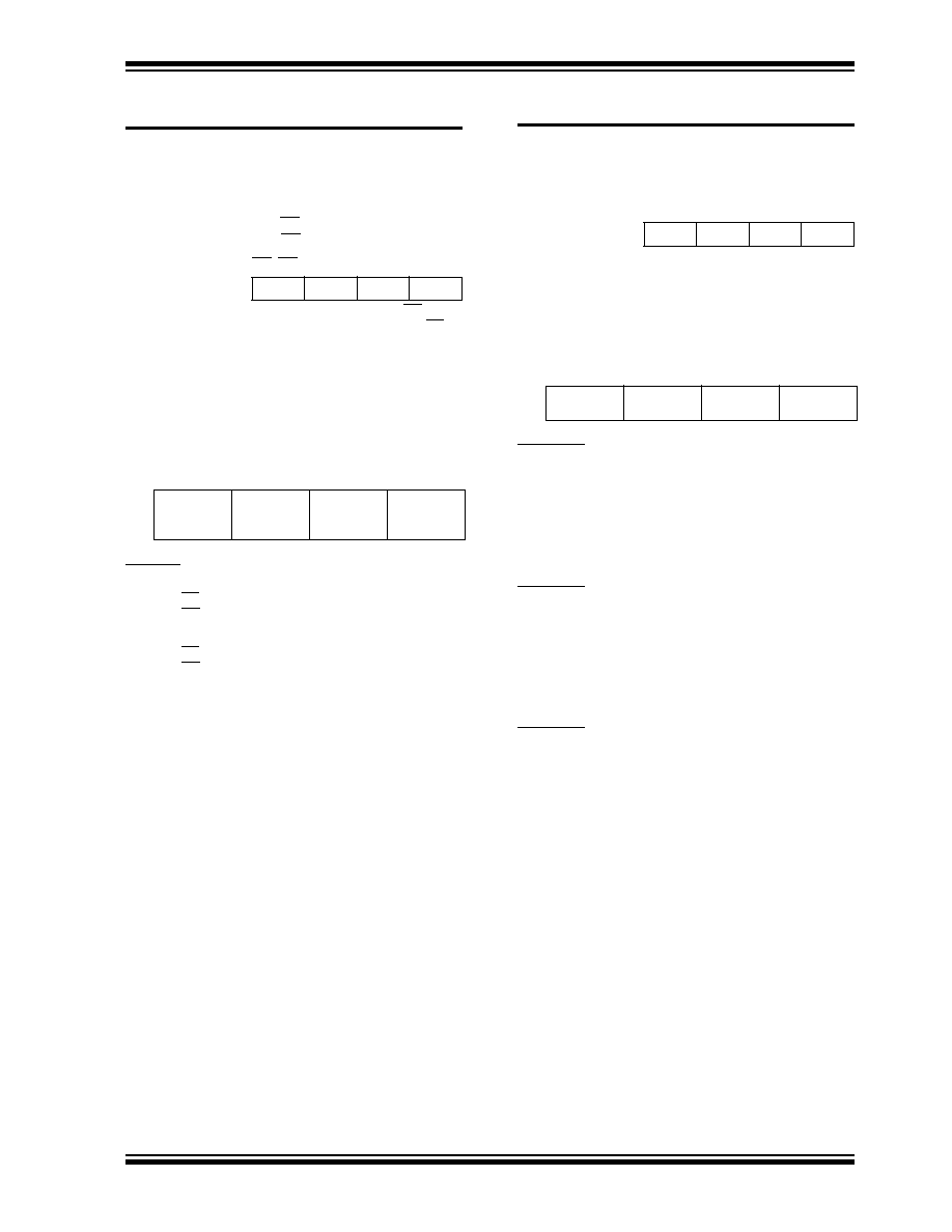
©
1996 Microchip Technology Inc.
DS30412C-page 135
PIC17C4X
SLEEP
Enter SLEEP mode
Syntax:
[
label ] SLEEP
Operands:
None
Operation:
00h
WDT;
0
WDT postscaler;
1
TO;
0
PD
Status Affected:
TO, PD
Encoding:
0000
0000
0000
0011
Description:
The power down status bit (PD) is
cleared. The time-out status bit (TO) is
set. Watchdog Timer and its prescaler
are cleared.
The processor is put into SLEEP
mode with the oscillator stopped.
Words:
1
Cycles:
1
Q Cycle Activity:
Q1
Q2
Q3
Q4
Decode
Read
register
PCLATH
Execute
NOP
Example:
SLEEP
Before Instruction
TO =
?
PD =
?
After Instruction
TO =
1
PD =
0
If WDT causes wake-up, this bit is cleared
SUBLW
Subtract WREG from Literal
Syntax:
[
label ] SUBLW k
Operands:
0
k
255
Operation:
k ≠ (WREG)
(
WREG)
Status Affected:
OV, C, DC, Z
Encoding:
1011
0010
kkkk
kkkk
Description:
WREG is subtracted from the eight bit
literal 'k'. The result is placed in
WREG.
Words:
1
Cycles:
1
Q Cycle Activity:
Q1
Q2
Q3
Q4
Decode
Read
literal 'k'
Execute
Write to
WREG
Example 1:
SUBLW
0x02
Before Instruction
WREG
=
1
C
=
?
After Instruction
WREG
=
1
C
=
1 ; result is positive
Z
=
0
Example 2:
Before Instruction
WREG
=
2
C
=
?
After Instruction
WREG
=
0
C
=
1 ; result is zero
Z
=
1
Example 3:
Before Instruction
WREG
=
3
C
=
?
After Instruction
WREG
=
FF ; (2's complement)
C
=
0 ; result is negative
Z
=
1
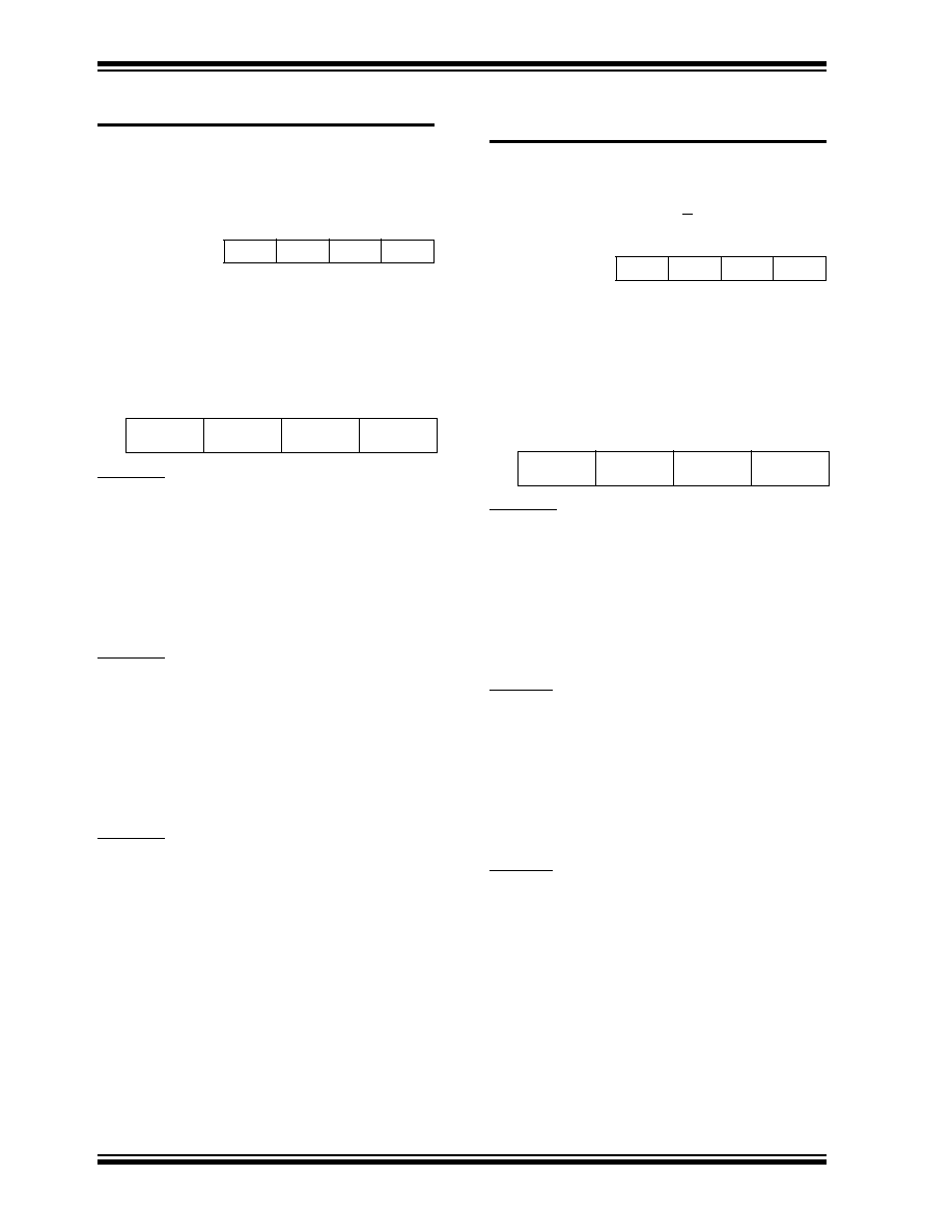
PIC17C4X
DS30412C-page 136
©
1996 Microchip Technology Inc.
SUBWF
Subtract WREG from f
Syntax:
[
label ] SUBWF f,d
Operands:
0
f
255
d
[0,1]
Operation:
(f) ≠ (W)
(
dest)
Status Affected:
OV, C, DC, Z
Encoding:
0000
010d
ffff
ffff
Description:
Subtract WREG from register 'f' (2's
complement method). If 'd' is 0 the
result is stored in WREG. If 'd' is 1 the
result is stored back in register 'f'.
Words:
1
Cycles:
1
Q Cycle Activity:
Q1
Q2
Q3
Q4
Decode
Read
register 'f'
Execute
Write to
destination
Example 1:
SUBWF REG1, 1
Before Instruction
REG1
=
3
WREG
=
2
C
=
?
After Instruction
REG1
=
1
WREG
=
2
C
=
1 ; result is positive
Z
=
0
Example 2:
Before Instruction
REG1
=
2
WREG
=
2
C
=
?
After Instruction
REG1
=
0
WREG
=
2
C
=
1 ; result is zero
Z
=
1
Example 3:
Before Instruction
REG1
=
1
WREG
=
2
C
=
?
After Instruction
REG1
=
FF
WREG
=
2
C
=
0 ; result is negative
Z
=
0
SUBWFB
Subtract WREG from f with
Borrow
Syntax:
[
label ] SUBWFB f,d
Operands:
0
f
255
d
[0,1]
Operation:
(f) ≠ (W) ≠ C
(
dest)
Status Affected:
OV, C, DC, Z
Encoding:
0000
001d
ffff
ffff
Description:
Subtract WREG and the carry flag
(borrow) from register 'f' (2's comple-
ment method). If 'd' is 0 the result is
stored in WREG. If 'd' is 1 the result is
stored back in register 'f'.
Words:
1
Cycles:
1
Q Cycle Activity:
Q1
Q2
Q3
Q4
Decode
Read
register 'f'
Execute
Write to
destination
Example 1:
SUBWFB REG1, 1
Before Instruction
REG1
=
0x19 (
0001 1001
)
WREG
=
0x0D (
0000 1101
)
C
=
1
After Instruction
REG1
=
0x0C (
0000 1011
)
WREG
=
0x0D (
0000 1101
)
C
=
1
; result is positive
Z
=
0
Example2:
SUBWFB
REG1,0
Before Instruction
REG1
=
0x1B (
0001 1011
)
WREG
=
0x1A (
0001 1010
)
C
=
0
After Instruction
REG1
=
0x1B
(
0001 1011
)
WREG
=
0x00
C
=
1
; result is zero
Z
=
1
Example3:
SUBWFB
REG1,1
Before Instruction
REG1
=
0x03 (
0000 0011
)
WREG
=
0x0E
(
0000 1101
)
C
=
1
After Instruction
REG1
=
0xF5
(
1111 0100
) [2's comp]
WREG
=
0x0E
(
0000 1101
)
C
=
0
; result is negative
Z
=
0
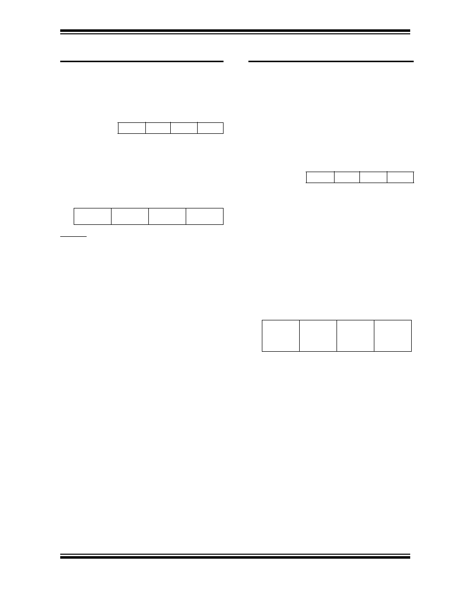
©
1996 Microchip Technology Inc.
DS30412C-page 137
PIC17C4X
SWAPF
Swap f
Syntax:
[
label ] SWAPF f,d
Operands:
0
f
255
d
[0,1]
Operation:
f<3:0>
dest<7:4>;
f<7:4>
dest<3:0>
Status Affected:
None
Encoding:
0001
110d
ffff
ffff
Description:
The upper and lower nibbles of register
'f' are exchanged. If 'd' is 0 the result is
placed in WREG. If 'd' is 1 the result is
placed in register 'f'.
Words:
1
Cycles:
1
Q Cycle Activity:
Q1
Q2
Q3
Q4
Decode
Read
register 'f'
Execute
Write to
destination
Example:
SWAPF
REG,
0
Before Instruction
REG
=
0x53
After Instruction
REG
=
0x35
TABLRD
Table Read
Syntax:
[
label ] TABLRD
t,i,f
Operands:
0
f
255
i
[0,1]
t
[0,1]
Operation:
If t = 1,
TBLATH
f;
If t = 0,
TBLATL
f;
Prog Mem (TBLPTR)
TBLAT;
If i = 1,
TBLPTR + 1
TBLPTR
Status Affected:
None
Encoding:
1010
10ti
ffff
ffff
Description:
1.
A byte of the table latch (TBLAT)
is moved to register file 'f'.
If t = 0: the high byte is moved;
If t = 1: the low byte is moved
2.
Then the contents of the program
memory location pointed to by
the 16-bit Table Pointer
(TBLPTR) is loaded into the
16-bit Table Latch (TBLAT).
3.
If i = 1: TBLPTR is incremented;
If i = 0: TBLPTR is not
incremented
Words:
1
Cycles:
2 (3 cycle if f = PCL)
Q Cycle Activity:
Q1
Q2
Q3
Q4
Decode
Read
register
TBLATH or
TBLATL
Execute
Write
register 'f'

PIC17C4X
DS30412C-page 138
©
1996 Microchip Technology Inc.
TABLRD
Table Read
Example1:
TABLRD 1, 1, REG ;
Before Instruction
REG
=
0x53
TBLATH
=
0xAA
TBLATL
=
0x55
TBLPTR
=
0xA356
MEMORY(TBLPTR)
=
0x1234
After Instruction (table write completion)
REG
=
0xAA
TBLATH
=
0x12
TBLATL
=
0x34
TBLPTR
=
0xA357
MEMORY(TBLPTR)
=
0x5678
Example2:
TABLRD 0, 0, REG ;
Before Instruction
REG
=
0x53
TBLATH
=
0xAA
TBLATL
=
0x55
TBLPTR
=
0xA356
MEMORY(TBLPTR)
=
0x1234
After Instruction (table write completion)
REG
=
0x55
TBLATH
=
0x12
TBLATL
=
0x34
TBLPTR
=
0xA356
MEMORY(TBLPTR)
=
0x1234
TABLWT
Table Write
Syntax:
[
label ] TABLWT
t,i,f
Operands:
0
f
255
i
[0,1]
t
[0,1]
Operation:
If t = 0,
f
TBLATL;
If t = 1,
f
TBLATH;
TBLAT
Prog Mem (TBLPTR);
If i = 1,
TBLPTR + 1
TBLPTR
Status Affected:
None
Encoding:
1010
11ti
ffff
ffff
Description:
1.
Load value in 'f' into 16-bit table
latch (TBLAT)
If t = 0: load into low byte;
If t = 1: load into high byte
2.
The contents of TBLAT is written
to the program memory location
pointed to by TBLPTR
If TBLPTR points to external
program memory location, then
the instruction takes two-cycle
If TBLPTR points to an internal
EPROM location, then the
instruction is terminated when
an interrupt is received.
Note:
The MCLR/V
PP
pin must be at the programming
voltage for successful programming of internal
memory.
If MCLR/V
PP
= V
DD
the programming sequence of internal memory
will be executed, but will not be successful
(although the internal memory location may be
disturbed)
3.
The TBLPTR can be automati-
cally incremented
If i = 0; TBLPTR is not
incremented
If i = 1; TBLPTR is incremented
Words:
1
Cycles:
2 (many if write is to on-chip
EPROM program memory)
Q Cycle Activity:
Q1
Q2
Q3
Q4
Decode
Read
register 'f'
Execute
Write
register
TBLATH or
TBLATL

©
1996 Microchip Technology Inc.
DS30412C-page 139
PIC17C4X
TABLWT
Table Write
Example1:
TABLWT 0, 1, REG
Before Instruction
REG
=
0x53
TBLATH
=
0xAA
TBLATL
=
0x55
TBLPTR
=
0xA356
MEMORY(TBLPTR)
=
0xFFFF
After Instruction (table write completion)
REG
=
0x53
TBLATH
=
0x53
TBLATL
=
0x55
TBLPTR
=
0xA357
MEMORY(TBLPTR - 1) =
0x5355
Example 2:
TABLWT 1, 0, REG
Before Instruction
REG
=
0x53
TBLATH
=
0xAA
TBLATL
=
0x55
TBLPTR
=
0xA356
MEMORY(TBLPTR)
=
0xFFFF
After Instruction (table write completion)
REG
=
0x53
TBLATH
=
0xAA
TBLATL
=
0x53
TBLPTR
=
0xA356
MEMORY(TBLPTR)
=
0xAA53
Program
Memory
16 bits
15
0
TBLPTR
TBLAT
Data
Memory
8 bits
15
8
7
0
TLRD
Table Latch Read
Syntax:
[
label ] TLRD
t,f
Operands:
0
f
255
t
[0,1]
Operation:
If t = 0,
TBLATL
f;
If t = 1,
TBLATH
f
Status Affected:
None
Encoding:
1010
00tx
ffff
ffff
Description:
Read data from 16-bit table latch
(TBLAT) into file register 'f'. Table Latch
is unaffected.
If t = 1; high byte is read
If t = 0; low byte is read
This instruction is used in conjunction
with
TABLRD
to transfer data from pro-
gram memory to data memory.
Words:
1
Cycles:
1
Q Cycle Activity:
Q1
Q2
Q3
Q4
Decode
Read
register
TBLATH or
TBLATL
Execute
Write
register 'f'
Example:
TLRD t, RAM
Before Instruction
t
=
0
RAM
=
?
TBLAT
=
0x00AF
(TBLATH = 0x00)
(TBLATL = 0xAF)
After Instruction
RAM
=
0xAF
TBLAT
=
0x00AF
(TBLATH = 0x00)
(TBLATL = 0xAF)
Before Instruction
t
=
1
RAM
=
?
TBLAT
=
0x00AF
(TBLATH = 0x00)
(TBLATL = 0xAF)
After Instruction
RAM
=
0x00
TBLAT
=
0x00AF
(TBLATH = 0x00)
(TBLATL = 0xAF)
Program
Memory
16 bits
15
0
TBLPTR
TBLAT
Data
Memory
8 bits
15
8
7
0
PIC17C4X
DS30412C-page 140
©
1996 Microchip Technology Inc.
TLWT
Table Latch Write
Syntax:
[
label ] TLWT t,f
Operands:
0
f
255
t
[0,1]
Operation:
If t = 0,
f
TBLATL;
If t = 1,
f
TBLATH
Status Affected:
None
Encoding:
1010
01tx
ffff
ffff
Description:
Data from file register 'f' is written into
the 16-bit table latch (TBLAT).
If t = 1; high byte is written
If t = 0; low byte is written
This instruction is used in conjunction
with
TABLWT
to transfer data from data
memory to program memory.
Words:
1
Cycles:
1
Q Cycle Activity:
Q1
Q2
Q3
Q4
Decode
Read
register 'f'
Execute
Write
register
TBLATH or
TBLATL
Example:
TLWT t, RAM
Before Instruction
t
=
0
RAM
=
0xB7
TBLAT
=
0x0000 (TBLATH = 0x00)
(TBLATL = 0x00)
After Instruction
RAM
=
0xB7
TBLAT
=
0x00B7 (TBLATH = 0x00)
(TBLATL = 0xB7)
Before Instruction
t
=
1
RAM
=
0xB7
TBLAT
=
0x0000 (TBLATH = 0x00)
(TBLATL = 0x00)
After Instruction
RAM
=
0xB7
TBLAT
=
0xB700 (TBLATH = 0xB7)
(TBLATL = 0x00)
TSTFSZ
Test f, skip if 0
Syntax:
[
label ] TSTFSZ f
Operands:
0
f
255
Operation:
skip if f = 0
Status Affected:
None
Encoding:
0011
0011
ffff
ffff
Description:
If 'f' = 0, the next instruction, fetched
during the current instruction execution,
is discarded and an NOP is executed
making this a two-cycle instruction.
Words:
1
Cycles:
1 (2)
Q Cycle Activity:
Q1
Q2
Q3
Q4
Decode
Read
register 'f'
Execute
NOP
If skip:
Q1
Q2
Q3
Q4
Forced NOP
NOP
Execute
NOP
Example:
HERE TSTFSZ CNT
NZERO :
ZERO :
Before Instruction
PC = Address(
HERE
)
After Instruction
If CNT
=
0x00,
PC =
Address
(ZERO)
If CNT
0x00,
PC =
Address
(NZERO)

©
1996 Microchip Technology Inc.
DS30412C-page 141
PIC17C4X
XORLW
Exclusive OR Literal with
WREG
Syntax:
[
label ] XORLW k
Operands:
0
k
255
Operation:
(WREG) .XOR. k
(
WREG)
Status Affected:
Z
Encoding:
1011
0100
kkkk
kkkk
Description:
The contents of WREG are XOR'ed
with the 8-bit literal 'k'. The result is
placed in WREG.
Words:
1
Cycles:
1
Q Cycle Activity:
Q1
Q2
Q3
Q4
Decode
Read
literal 'k'
Execute
Write to
WREG
Example:
XORLW
0xAF
Before Instruction
WREG
=
0xB5
After Instruction
WREG
=
0x1A
XORWF
Exclusive OR WREG with f
Syntax:
[
label ] XORWF f,d
Operands:
0
f
255
d
[0,1]
Operation:
(WREG) .XOR. (f)
(
dest)
Status Affected:
Z
Encoding:
0000
110d
ffff
ffff
Description:
Exclusive OR the contents of WREG
with register 'f'. If 'd' is 0 the result is
stored in WREG. If 'd' is 1 the result is
stored back in the register 'f'.
Words:
1
Cycles:
1
Q Cycle Activity:
Q1
Q2
Q3
Q4
Decode
Read
register 'f'
Execute
Write to
destination
Example:
XORWF REG, 1
Before Instruction
REG
=
0xAF
WREG
=
0xB5
After Instruction
REG
=
0x1A
WREG
=
0xB5

PIC17C4X
DS30412C-page 142
©
1996 Microchip Technology Inc.
NOTES:

©
1996 Microchip Technology Inc.
DS30412C-page 143
PIC17C4X
16.0
DEVELOPMENT SUPPORT
16.1
Development Tools
The PIC16/17 microcontrollers are supported with a full
range of hardware and software development tools:
∑ PICMASTER/PICMASTER CE
Real-Time
In-Circuit Emulator
∑ ICEPIC Low-Cost PIC16C5X and PIC16CXXX
In-Circuit Emulator
∑ PRO MATE
Æ
II Universal Programmer
∑ PICSTART
Æ
Plus Entry-Level Prototype
Programmer
∑ PICDEM-1 Low-Cost Demonstration Board
∑ PICDEM-2 Low-Cost Demonstration Board
∑ PICDEM-3 Low-Cost Demonstration Board
∑ MPASM Assembler
∑ MPLAB-SIM Software Simulator
∑ MPLAB-C (C Compiler)
∑ Fuzzy logic development system (fuzzyTECH
Æ
-
MP)
16.2
PICMASTER: High Performance
Universal In-Circuit Emulator with
MPLAB IDE
The PICMASTER Universal In-Circuit Emulator is
intended to provide the product development engineer
with a complete microcontroller design tool set for all
microcontrollers in the PIC12C5XX, PIC14000,
PIC16C5X, PIC16CXXX and PIC17CXX families.
PICMASTER is supplied with the MPLAB
TM
Integrated
Development Environment (IDE), which allows editing,
"make" and download, and source debugging from a
single environment.
Interchangeable target probes allow the system to be
easily reconfigured for emulation of different proces-
sors. The universal architecture of the PICMASTER
allows expansion to support all new Microchip micro-
controllers.
The PICMASTER Emulator System has been
designed as a real-time emulation system with
advanced features that are generally found on more
expensive development tools. The PC compatible 386
(and higher) machine platform and Microsoft Windows
Æ
3.x environment were chosen to best make these fea-
tures available to you, the end user.
A CE compliant version of PICMASTER is available for
European Union (EU) countries.
16.3
ICEPIC: Low-cost PIC16CXXX
In-Circuit Emulator
ICEPIC is a low-cost in-circuit emulator solution for the
Microchip PIC16C5X and PIC16CXXX families of 8-bit
OTP microcontrollers.
ICEPIC is designed to operate on PC-compatible
machines ranging from 286-AT
Æ
through Pentium
TM
based machines under Windows 3.x environment.
ICEPIC features real time, non-intrusive emulation.
16.4
PRO MATE II: Universal Programmer
The PRO MATE II Universal Programmer is a full-fea-
tured programmer capable of operating in stand-alone
mode as well as PC-hosted mode.
The PRO MATE II has programmable V
DD
and V
PP
supplies which allows it to verify programmed memory
at V
DD
min and V
DD
max for maximum reliability. It has
an LCD display for displaying error messages, keys to
enter commands and a modular detachable socket
assembly to support various package types. In stand-
alone mode the PRO MATE II can read, verify or pro-
gram PIC16C5X, PIC16CXXX, PIC17CXX and
PIC14000 devices. It can also set configuration and
code-protect bits in this mode.
16.5
PICSTART Plus Entry Level
Development System
The PICSTART programmer is an easy-to-use, low-
cost prototype programmer. It connects to the PC via
one of the COM (RS-232) ports. MPLAB Integrated
Development Environment software makes using the
programmer simple and efficient. PICSTART Plus is
not recommended for production programming.
PICSTART Plus supports all PIC12C5XX, PIC14000,
PIC16C5X, PIC16CXXX and PIC17CXX devices with
up to 40 pins. Larger pin count devices such as the
PIC16C923 and PIC16C924 may be supported with an
adapter socket.
This document was created with FrameMaker 4 0 4

PIC17C4X
DS30412C-page 144
©
1996 Microchip Technology Inc.
16.6
PICDEM-1 Low-Cost PIC16/17
Demonstration Board
The PICDEM-1 is a simple board which demonstrates
the capabilities of several of Microchip's microcontrol-
lers. The microcontrollers supported are: PIC16C5X
(PIC16C54 to PIC16C58A), PIC16C61, PIC16C62X,
PIC16C71, PIC16C8X, PIC17C42, PIC17C43 and
PIC17C44. All necessary hardware and software is
included to run basic demo programs. The users can
program the sample microcontrollers provided with
the PICDEM-1 board, on a PRO
MATE II or
PICSTART-16B programmer, and easily test firm-
ware. The user can also connect the PICDEM-1
board to the PICMASTER emulator and download
the firmware to the emulator for testing. Additional pro-
totype area is available for the user to build some addi-
tional hardware and connect it to the microcontroller
socket(s). Some of the features include an RS-232
interface, a potentiometer for simulated analog input,
push-button switches and eight LEDs connected to
PORTB.
16.7
PICDEM-2 Low-Cost PIC16CXX
Demonstration Board
The PICDEM-2 is a simple demonstration board that
supports the PIC16C62, PIC16C64, PIC16C65,
PIC16C73 and PIC16C74 microcontrollers. All the
necessary hardware and software is included to
run the basic demonstration programs. The user
can program the sample microcontrollers provided
with the PICDEM-2 board, on a PRO MATE II pro-
grammer or PICSTART-16C, and easily test firmware.
The PICMASTER emulator may also be used with the
PICDEM-2 board to test firmware. Additional prototype
area has been provided to the user for adding addi-
tional hardware and connecting it to the microcontroller
socket(s). Some of the features include a RS-232 inter-
face, push-button switches, a potentiometer for simu-
lated analog input, a Serial EEPROM to demonstrate
usage of the I
2
C bus and separate headers for connec-
tion to an LCD module and a keypad.
16.8
PICDEM-3 Low-Cost PIC16CXXX
Demonstration Board
The PICDEM-3 is a simple demonstration board that
supports the PIC16C923 and PIC16C924 in the PLCC
package. It will also support future 44-pin PLCC
microcontrollers with a LCD Module. All the neces-
sary hardware and software is included to run the
basic demonstration programs. The user can pro-
gram the sample microcontrollers provided with
the PICDEM-3 board, on a PRO MATE II program-
mer or PICSTART Plus with an adapter socket, and
easily test firmware. The PICMASTER emulator may
also be used with the PICDEM-3 board to test firm-
ware. Additional prototype area has been provided to
the user for adding hardware and connecting it to the
microcontroller socket(s). Some of the features
include an RS-232 interface, push-button switches, a
potentiometer for simulated analog input, a thermistor
and separate headers for connection to an external
LCD module and a keypad. Also provided on the
PICDEM-3 board is an LCD panel, with 4 commons
and 12 segments, that is capable of displaying time,
temperature and day of the week. The PICDEM-3 pro-
vides an additional RS-232 interface and Windows 3.1
software for showing the demultiplexed LCD signals on
a PC. A simple serial interface allows the user to con-
struct a hardware demultiplexer for the LCD signals.
PICDEM-3 will be available in the 3rd quarter of 1996.
16.9
MPLAB Integrated Development
Environment Software
The MPLAB IDE Software brings an ease of software
development previously unseen in the 8-bit microcon-
troller market. MPLAB is a windows based application
which contains:
∑ A full featured editor
∑ Three operating modes
- editor
- emulator
- simulator
∑ A project manager
∑ Customizable tool bar and key mapping
∑ A status bar with project information
∑ Extensive on-line help
MPLAB allows you to:
∑ Edit your source files (either assembly or `C')
∑ One touch assemble (or compile) and download
to PIC16/17 tools (automatically updates all
project information)
∑ Debug using:
- source files
- absolute listing file
∑ Transfer data dynamically via DDE (soon to be
replaced by OLE)
∑ Run up to four emulators on the same PC
The ability to use MPLAB with Microchip's simulator
allows a consistent platform and the ability to easily
switch from the low cost simulator to the full featured
emulator with minimal retraining due to development
tools.
16.10
Assembler (MPASM)
The MPASM Universal Macro Assembler is a PC-
hosted symbolic assembler. It supports all microcon-
troller series including the PIC12C5XX, PIC14000,
PIC16C5X, PIC16CXXX, and PIC17CXX families.
MPASM offers full featured Macro capabilities, condi-
tional assembly, and several source and listing formats.
It generates various object code formats to support
Microchip's development tools as well as third party
programmers.

©
1996 Microchip Technology Inc.
DS30412C-page 145
PIC17C4X
MPASM allow full symbolic debugging from the
Microchip Universal Emulator System
(PICMASTER).
MPASM has the following features to assist in develop-
ing software for specific use applications.
∑ Provides translation of Assembler source code to
object code for all Microchip microcontrollers.
∑ Macro assembly capability.
∑ Produces all the files (Object, Listing, Symbol,
and special) required for symbolic debug with
Microchip's emulator systems.
∑ Supports Hex (default), Decimal and Octal
source and listing formats.
MPASM provides a rich directive language to support
programming of the PIC16/17. Directives are helpful in
making the development of your assemble source
code shorter and more maintainable.
16.11
Software Simulator (MPLAB-SIM)
The MPLAB-SIM Software Simulator allows code
development in a PC host environment. It allows the
user to simulate the PIC16/17 series microcontrollers
on an instruction level. On any given instruction, the
user may examine or modify any of the data areas or
provide external stimulus to any of the pins. The input/
output radix can be set by the user and the execution
can be performed in; single step, execute until break,
or in a trace mode.
MPLAB-SIM fully supports symbolic debugging using
MPLAB-C and MPASM. The Software Simulator offers
the low cost flexibility to develop and debug code out-
side of the laboratory environment making it an excel-
lent multi-project software development tool.
16.12
C Compiler (MPLAB-C)
The MPLAB-C Code Development System is a
complete `C' compiler and integrated development
environment for Microchip's PIC16/17 family of micro-
controllers. The compiler provides powerful integration
capabilities and ease of use not found with other
compilers.
For easier source level debugging, the compiler pro-
vides symbol information that is compatible with the
MPLAB IDE memory display (PICMASTER emulator
software versions 1.13 and later).
16.13
Fuzzy Logic Development System
(
fuzzy
TECH-MP)
fuzzy
TECH-MP fuzzy logic development tool is avail-
able in two versions - a low cost introductory version,
MP Explorer, for designers to gain a comprehensive
working knowledge of fuzzy logic system design; and a
full-featured version,
fuzzy
TECH-MP, edition for imple-
menting more complex systems.
Both versions include Microchip's
fuzzy
LAB
TM
demon-
stration board for hands-on experience with fuzzy logic
systems implementation.
16.14
MP-DriveWay
TM
≠ Application Code
Generator
MP-DriveWay is an easy-to-use Windows-based Appli-
cation Code Generator. With MP-DriveWay you can
visually configure all the peripherals in a PIC16/17
device and, with a click of the mouse, generate all the
initialization and many functional code modules in C
language. The output is fully compatible with Micro-
chip's MPLAB-C C compiler. The code produced is
highly modular and allows easy integration of your own
code. MP-DriveWay is intelligent enough to maintain
your code through subsequent code generation.
16.15
SEEVAL
Æ
Evaluation and
Programming System
The SEEVAL SEEPROM Designer's Kit supports all
Microchip 2-wire and 3-wire Serial EEPROMs. The kit
includes everything necessary to read, write, erase or
program special features of any Microchip SEEPROM
product including Smart Serials
TM
and secure serials.
The Total Endurance
TM
Disk is included to aid in trade-
off analysis and reliability calculations. The total kit can
significantly reduce time-to-market and result in an
optimized system.
16.16
TrueGauge
Æ
Intelligent Battery
Management
The TrueGauge development tool supports system
development with the MTA11200B TrueGauge Intelli-
gent Battery Management IC. System design verifica-
tion can be accomplished before hardware prototypes
are built. User interface is graphically-oriented and
measured data can be saved in a file for exporting to
Microsoft Excel.
16.17
K
EE
L
OQ
Æ
Evaluation and
Programming Tools
K
EE
L
OQ
evaluation and programming tools support
Microchips HCS Secure Data Products. The HCS eval-
uation kit includes an LCD display to show changing
codes, a decoder to decode transmissions, and a pro-
gramming interface to program test transmitters.

PIC17C4X
DS30412C-page 146
©
1996 Microchip Technology Inc.
TABLE 16-1:
DEVELOPMENT TOOLS FROM MICROCHIP
Pr
oduct
** MPLAB
TM
Integrated
De
velopment
En
vir
onment
MPLAB
TM
C
Compiler
MP-DriveW
a
y
Applications
Code
Generator
fuzzyTECH
Æ
-MP
Explorer/Edition
Fuzzy Logic
De
v
.
T
ool
*** PICMASTER
Æ
/
PICMASTER-CE
In-Cir
cuit
Em
ulator
ICEPIC
Lo
w-Cost
In-Cir
cuit
Em
ulator
****PR
O MA
TE
TM
II Univer
sal
Micr
oc
hip
Pr
ogrammer
PICST
AR
T
Æ
Lite
Ultra Lo
w-Cost
De
v
.
Kit
PICST
AR
T
Æ
Plus
Lo
w-Cost
Univer
sal
De
v
.
Kit
PIC12C508, 509
SW007002
SW006005
--
--
EM167015/
EM167101
--
D
V007003
--
D
V003001
PIC14000
SW007002
SW006005
--
--
EM147001/
EM147101
--
D
V007003
--
D
V003001
PIC16C52, 54, 54A,
55, 56, 57, 58A
SW007002
SW006005
SW006006
D
V005001/
D
V005002
EM167015/
EM167101
EM167201
D
V007003
D
V162003
D
V003001
PIC16C554, 556, 558
SW007002
SW006005
--
D
V005001/
D
V005002
EM167033/
EM167113
---
D
V007003
--
D
V003001
PIC16C61
SW007002
SW006005
SW006006
D
V005001/
D
V005002
EM167021/
N/A
EM167205
D
V007003
D
V162003
D
V003001
PIC16C62, 62A,
64, 64A
SW007002
SW006005
SW006006
D
V005001/
D
V005002
EM167025/
EM167103
EM167203
D
V007003
D
V162002
D
V003001
PIC16C620, 621, 622
SW007002
SW006005
SW006006
D
V005001/
D
V005002
EM167023/
EM167109
EM167202
D
V007003
D
V162003
D
V003001
PIC16C63, 65, 65A,
73, 73A, 74, 74A
SW007002
SW006005
SW006006
D
V005001/
D
V005002
EM167025/
EM167103
EM167204
D
V007003
D
V162002
D
V003001
PIC16C642, 662*
SW007002
SW006005
--
--
EM167035/
EM167105
---
D
V007003
D
V162002
D
V003001
PIC16C71
SW007002
SW006005
SW006006
D
V005001/
D
V005002
EM167027/
EM167105
EM167205
D
V007003
D
V162003
D
V003001
PIC16C710, 711
SW007002
SW006005
SW006006
D
V005001/
D
V005002
EM167027/
EM167105
--
D
V007003
D
V162003
D
V003001
PIC16C72
SW007002
SW006005
SW006006
--
EM167025/
EM167103
--
D
V007003
D
V162002
D
V003001
PIC16F83
SW007002
SW006005
SW006006
D
V005001/
D
V005002
EM167029/
EM167107
--
D
V007003
D
V162003
D
V003001
PIC16C84
SW007002
SW006005
SW006006
D
V005001/
D
V005002
EM167029/
EM167107
EM167206
D
V007003
D
V162003
D
V003001
PIC16F84
SW007002
SW006005
SW006006
D
V005001/
D
V005002
EM167029/
EM167107
--
D
V007003
D
V162003
D
V003001
PIC16C923, 924*
SW007002
SW006005
SW006006
D
V005001/
D
V005002
EM167031/
EM167111
--
D
V007003
--
D
V003001
PIC17C42,
42A, 43, 44
SW007002
SW006005
SW006006
D
V005001/
D
V005002
EM177007/
EM177107
--
D
V007003
--
D
V003001
*Contact Microchip
T
echnology f
or a
v
ailability date
**MPLAB Integ
r
ated De
v
elopment En
vironment includes MPLAB-SIM Sim
ulator and
MP
ASM Assemb
ler
***All PICMASTER and PICMASTER-CE order
ing par
t n
umbers abo
v
e
include
PR
O MA
TE II prog
r
ammer
****PR
O MA
TE soc
k
et modules are ordered separ
ately
.
See de
v
elopment systems
ordering guide f
or specifi
c order
ing par
t n
umbers
Pr
oduct
TR
UEGA
UGE
Æ
De
velopment Kit
SEEV
AL
Æ
Designer
s Kit
Hopping Code Security Pr
ogrammer Kit
Hopping Code Security Ev
al/Demo Kit
All 2 wire and 3 wire
Ser
ial EEPR
OM's
N/A
D
V243001
N/A
N/A
MT
A11200B
D
V114001
N/A
N/A
N/A
HCS200, 300, 301 *
N/A
N/A
PG306001
DM303001

©
1996 Microchip Technology Inc.
DS30412C-page 147
PIC17C4X
Applicable Devices
42 R42 42A 43 R43 44
17.0
PIC17C42 ELECTRICAL CHARACTERISTICS
Absolute Maximum Ratings
Ambient temperature under bias..................................................................................................................-55 to +125∞C
Storage temperature ............................................................................................................................... -65∞C to +150∞C
Voltage on V
DD
with respect to V
SS
................................................................................................................ 0 to +7.5V
Voltage on MCLR with respect to V
SS
(Note 2) ..........................................................................................-0.6V to +14V
Voltage on RA2 and RA3 with respect to V
SS
..............................................................................................-0.6V to +12V
Voltage on all other pins with respect to V
SS
..................................................................................... -0.6V to V
DD
+ 0.6V
Total power dissipation (Note 1).................................................................................................................................1.0W
Maximum current out of V
SS
pin(s) - Total .............................................................................................................250 mA
Maximum current into V
DD
pin(s) - Total ................................................................................................................200 mA
Input clamp current, I
IK
(V
I
< 0 or V
I
> V
DD
)
......................................................................................................................±
20 mA
Output clamp current, I
OK
(V
O
< 0 or V
O
> V
DD
)
...............................................................................................................±
20 mA
Maximum output current sunk by any I/O pin (except RA2 and RA3)......................................................................35 mA
Maximum output current sunk by RA2 or RA3 pins .................................................................................................60 mA
Maximum output current sourced by any I/O pin .....................................................................................................20 mA
Maximum current sunk by
PORTA and PORTB (combined) ..................................................................................150 mA
Maximum current sourced by PORTA and PORTB (combined).............................................................................100 mA
Maximum current sunk by PORTC, PORTD and PORTE (combined)...................................................................150 mA
Maximum current sourced by PORTC, PORTD and PORTE (combined)..............................................................100 mA
Note 1:
Power dissipation is calculated as follows: Pdis = V
DD
x {I
DD
-
I
OH
} +
{(V
DD
-V
OH
) x I
OH
} +
(V
OL
x I
OL
)
Note 2:
Voltage spikes below V
SS
at the MCLR pin, inducing currents greater than 80 mA, may cause latch-up.
Thus, a series resistor of 50-100
should be used when applying a "low" level to the MCLR pin rather than
pulling this pin directly to V
SS
.
NOTICE: Stresses above those listed under "Absolute Maximum Ratings" may cause permanent damage to the
device. This is a stress rating only and functional operation of the device at those or any other conditions above
those indicated in the operation listings of this specification is not implied. Exposure to maximum rating conditions for
extended periods may affect device reliability.
This document was created with FrameMaker 4 0 4

PIC17C4X
DS30412C-page 148
©
1996 Microchip Technology Inc.
Applicable Devices
42 R42 42A 43 R43 44
TABLE 17-1:
CROSS REFERENCE OF DEVICE SPECS FOR OSCILLATOR CONFIGURATIONS
AND FREQUENCIES OF OPERATION (COMMERCIAL DEVICES)
OSC
PIC17C42-16
PIC17C42-25
RC
V
DD
: 4.5V to 5.5V
I
DD
: 6 mA max.
I
PD
: 5
µ
A max. at 5.5V (WDT disabled)
Freq: 4 MHz max.
V
DD
: 4.5V to 5.5V
I
DD
: 6 mA max.
I
PD
: 5
µ
A max. at 5.5V (WDT disabled)
Freq: 4 MHz max.
XT
V
DD
: 4.5V to 5.5V
I
DD
: 24 mA max.
I
PD
: 5
µ
A max. at 5.5V (WDT disabled)
Freq: 16 MHz max.
V
DD
: 4.5V to 5.5V
I
DD
: 38 mA max.
I
PD
: 5
µ
A max. at 5.5V (WDT disabled)
Freq: 25 MHz max.
EC
V
DD
: 4.5V to 5.5V
I
DD
: 24 mA max.
I
PD
: 5
µ
A max. at 5.5V (WDT disabled)
Freq: 16 MHz max.
V
DD
: 4.5V to 5.5V
I
DD
: 38 mA max.
I
PD
: 5
µ
A max. at 5.5V (WDT disabled)
Freq: 25 MHz max.
LF
V
DD
: 4.5V to 5.5V
I
DD
: 150
µ
A max. at 32 kHz (WDT enabled)
I
PD
: 5
µ
A max. at 5.5V (WDT disabled)
Freq: 2 MHz max.
V
DD
: 4.5V to 5.5V
I
DD
: 150
µ
A max. at 32 kHz (WDT enabled)
I
PD
: 5
µ
A max. at 5.5V (WDT disabled)
Freq: 2 MHz max.
©
1996 Microchip Technology Inc.
DS30412C-page 149
PIC17C4X
Applicable Devices
42 R42 42A 43 R43 44
17.1
DC CHARACTERISTICS:
PIC17C42-16 (Commercial, Industrial)
PIC17C42-25 (Commercial, Industrial)
DC CHARACTERISTICS
Standard Operating Conditions (unless otherwise stated)
Operating temperature
-40∞C
T
A
+85∞C for industrial and
0∞C
T
A
+70∞C for commercial
Parameter
No.
Sym
Characteristic
Min
Typ
Max
Units
Conditions
D001
V
DD
Supply Voltage
4.5
≠
5.5
V
D002
V
DR
RAM Data Retention
Voltage (Note 1)
1.5 *
≠
≠
V
Device in SLEEP mode
D003
V
POR
V
DD
start voltage to
ensure internal
Power-on Reset signal
≠
V
SS
≠
V
See section on Power-on Reset for
details
D004
S
VDD
V
DD
rise rate to
ensure internal
Power-on Reset signal
0.060*
≠
≠
mV/ms See section on Power-on Reset for
details
D010
D011
D012
D013
D014
I
DD
Supply Current
(Note 2)
≠
≠
≠
≠
≠
3
6
11
19
95
6
12 *
24 *
38
150
mA
mA
mA
mA
µ
A
F
OSC
= 4 MHz (Note 4)
F
OSC
= 8 MHz
F
OSC
= 16 MHz
F
OSC
= 25 MHz
F
OSC
= 32 kHz
WDT enabled (EC osc configuration)
D020
D021
I
PD
Power-down Current
(Note 3)
≠
≠
10
< 1
40
5
µ
A
µ
A
V
DD
= 5.5V, WDT enabled
V
DD
= 5.5V, WDT disabled
*
These parameters are characterized but not tested.
Data in "Typ" column is at 5V, 25∞C unless otherwise stated. These parameters are for design guidance
only and are not tested.
Note 1: This is the limit to which V
DD
can be lowered in SLEEP mode without losing RAM data.
2: The supply current is mainly a function of the operating voltage and frequency. Other factors such as I/O pin
loading and switching rate, oscillator type, internal code execution pattern, and temperature also have an
impact on the current consumption.
The test conditions for all I
DD
measurements in active operation mode are:
OSC1 = external square wave, from rail to rail; all I/O pins tristated, pulled to V
DD
or V
SS
, T0CKI = V
DD
,
MCLR = V
DD
; WDT enabled/disabled as specified.
Current consumed from the oscillator and I/O's driving external capacitive or resistive loads need to be con-
sidered.
For the RC oscillator, the current through the external pull-up resistor (R) can be estimated as: V
DD
/ (2
∑
R).
For capacitive loads, The current can be estimated (for an individual I/O pin) as (C
L
∑
V
DD
)
∑
f
C
L
= Total capacitive load on the I/O pin; f = average frequency on the I/O pin switches.
The capacitive currents are most significant when the device is configured for external execution (includes
extended microcontroller mode).
3: The power-down current in SLEEP mode does not depend on the oscillator type. Power-down current is
measured with the part in SLEEP mode, all I/O pins in hi-impedance state and tied to V
DD
or V
SS
.
4: For RC osc configuration, current through Rext is not included. The current through the resistor can be esti-
mated by the formula I
R
= V
DD
/2Rext (mA) with Rext in kOhm.

PIC17C4X
DS30412C-page 150
©
1996 Microchip Technology Inc.
Applicable Devices
42 R42 42A 43 R43 44
17.2
DC CHARACTERISTICS:
PIC17C42-16 (Commercial, Industrial)
PIC17C42-25 (Commercial, Industrial)
DC CHARACTERISTICS
Standard Operating Conditions (unless otherwise stated)
Operating temperature
-40∞C
T
A
+85∞C for industrial and
0∞C
T
A
+70∞C for commercial
Operating voltage V
DD
range as described in Section 17.1
Parameter
No.
Sym
Characteristic
Min
Typ
Max
Units
Conditions
Input Low Voltage
V
IL
I/O ports
D030
with TTL buffer
V
SS
≠
0.8
V
D031
with Schmitt Trigger buffer
V
SS
≠
0.2V
DD
V
D032
MCLR, OSC1 (in EC and RC
mode)
Vss
≠
0.2V
DD
V
Note1
D033
OSC1 (in XT, and LF mode)
≠
0.5V
DD
≠
V
Input High Voltage
V
IH
I/O ports
≠
D040
with TTL buffer
2.0
≠
V
DD
V
D041
with Schmitt Trigger buffer
0.8V
DD
≠
V
DD
V
D042
MCLR
0.8V
DD
≠
V
DD
V
Note1
D043
OSC1 (XT, and LF mode)
≠
0.5V
DD
≠
V
D050
V
HYS
Hysteresis of
Schmitt Trigger inputs
0.15V
DD
*
≠
≠
V
Input Leakage Current
(Notes 2, 3)
D060
I
IL
I/O ports (except RA2, RA3)
≠
≠
±
1
µ
A
Vss
V
PIN
V
DD
,
I/O Pin at hi-impedance
PORTB weak pull-ups dis-
abled
D061
MCLR
≠
≠
±
2
µ
A
V
PIN
=
Vss or
V
PIN
=
V
DD
D062
RA2, RA3
±
2
µ
A
Vss
V
RA
2, V
RA
3
12V
D063
OSC1, TEST
≠
≠
±
1
µ
A
Vss
V
PIN
V
DD
D064
MCLR
≠
≠
10
µ
A
V
MCLR
= V
PP
= 12V
(when not programming)
D070
I
PURB
PORTB weak pull-up current
60
200
400
µ
A
V
PIN
= V
SS
, RBPU = 0
*
These parameters are characterized but not tested.
Data in "Typ" column is at 5V, 25
∞
C unless otherwise stated. These parameters are for design guidance only
and are not tested.
These parameters are for design guidance only and are not tested, nor characterized.
Design guidance to attain the AC timing specifications. These loads are not tested.
Note 1: In RC oscillator configuration, the OSC1 pin is a Schmitt Trigger input. It is not recommended that the
PIC17CXX devices be driven with external clock in RC mode.
2: The leakage current on the MCLR pin is strongly dependent on the applied voltage level. The specified levels
represent normal operating conditions. Higher leakage current may be measured at different input voltages.
3: Negative current is defined as coming out of the pin.
4: These specifications are for the programming of the on-chip program memory EPROM through the use of the
table write instructions. The complete programming specifications can be found in: PIC17CXX Programming
Specifications (Literature number DS30139).
5: The MCLR/Vpp pin may be kept in this range at times other than programming, but this is not recommended.
6: For TTL buffers, the better of the two specifications may be used.
©
1996 Microchip Technology Inc.
DS30412C-page 151
PIC17C4X
Applicable Devices 42 R42 42A 43 R43 44
Output Low Voltage
D080
D081
V
OL
I/O ports (except RA2 and RA3)
with TTL buffer
≠
≠
≠
≠
0.1V
DD
0.4
V
V
I
OL
= 4 mA
I
OL
= 6 mA, V
DD
= 4.5V
Note 6
D082
RA2 and RA3
≠
≠
3.0
V
I
OL
= 60.0 mA, V
DD
= 5.5V
D083
OSC2/CLKOUT
(RC and EC osc modes)
≠
≠
0.4
V
I
OL
= 2 mA, V
DD
= 4.5V
Output High Voltage (Note 3)
D090
D091
V
OH
I/O ports (except RA2 and RA3)
with TTL buffer
0.9V
DD
2.4
≠
≠
≠
≠
V
V
I
OH
= -2 mA
I
OH
= -6.0 mA, V
DD
= 4.5V
Note 6
D092
RA2 and RA3
≠
≠
12
V
Pulled-up to externally applied
voltage
D093
OSC2/CLKOUT
(RC and EC osc modes)
2.4
≠
≠
V
I
OH
= -5 mA, V
DD
= 4.5V
Capacitive Loading Specs on
Output Pins
D100
C
OSC2
OSC2 pin
≠
≠
25
pF
In EC or RC osc modes when
OSC2 pin is outputting
CLKOUT.
External clock is used to drive
OSC1.
D101
C
IO
All I/O pins and OSC2
(in RC mode)
≠
≠
50
pF
D102
C
AD
System Interface Bus
(PORTC, PORTD and PORTE)
≠
≠
100
pF
In Microprocessor or
Extended Microcontroller
mode
DC CHARACTERISTICS
Standard Operating Conditions (unless otherwise stated)
Operating temperature
-40∞C
T
A
+85∞C for industrial and
0∞C
T
A
+70∞C for commercial
Operating voltage V
DD
range as described in Section 17.1
Parameter
No.
Sym
Characteristic
Min
Typ
Max
Units
Conditions
*
These parameters are characterized but not tested.
Data in "Typ" column is at 5V, 25
∞
C unless otherwise stated. These parameters are for design guidance only
and are not tested.
These parameters are for design guidance only and are not tested, nor characterized.
Design guidance to attain the AC timing specifications. These loads are not tested.
Note 1: In RC oscillator configuration, the OSC1 pin is a Schmitt Trigger input. It is not recommended that the
PIC17CXX devices be driven with external clock in RC mode.
2: The leakage current on the MCLR pin is strongly dependent on the applied voltage level. The specified levels
represent normal operating conditions. Higher leakage current may be measured at different input voltages.
3: Negative current is defined as coming out of the pin.
4: These specifications are for the programming of the on-chip program memory EPROM through the use of the
table write instructions. The complete programming specifications can be found in: PIC17CXX Programming
Specifications (Literature number DS30139).
5: The MCLR/Vpp pin may be kept in this range at times other than programming, but this is not recommended.
6: For TTL buffers, the better of the two specifications may be used.

PIC17C4X
DS30412C-page 152
©
1996 Microchip Technology Inc.
Applicable Devices 42 R42 42A 43 R43 44
DC CHARACTERISTICS
Standard Operating Conditions (unless otherwise stated)
Operating temperature
-40∞C
T
A
+40∞C
Operating voltage V
DD
range as described in Section 17.1
Parameter
No.
Sym
Characteristic
Min
Typ
Max
Units
Conditions
Internal Program Memory
Programming Specs (Note 4)
D110
D111
D112
D113
D114
V
PP
V
DDP
I
PP
I
DDP
T
PROG
Voltage on MCLR/V
PP
pin
Supply voltage during
programming
Current into MCLR/V
PP
pin
Supply current during
programming
Programming pulse width
12.75
4.75
≠
≠
10
≠
5.0
25
≠
100
13.25
5.25
50
30
1000
V
V
mA
mA
µ
s
Note 5
Terminated via internal/exter-
nal interrupt or a reset
*
These parameters are characterized but not tested.
Data in "Typ" column is at 5V, 25
∞
C unless otherwise stated. These parameters are for design guidance only and
are not tested.
These parameters are for design guidance only and are not tested, nor characterized.
Note 1: In RC oscillator configuration, the OSC1/CLKIN pin is a Schmitt Trigger input. It is not recommended that the
PIC17CXX devices be driven with external clock in RC mode.
2: The leakage current on the MCLR pin is strongly dependent on the applied voltage level. The specified levels
represent normal operating conditions. Higher leakage current may be measured at different input voltages.
3: Negative current is defined as coming out of the pin.
4: These specifications are for the programming of the on-chip program memory EPROM through the use of the
table write instructions. The complete programming specifications can be found in: PIC17CXX Programming
Specifications (Literature number DS30139).
5: The MCLR/V
PP
pin may be kept in this range at times other than programming, but is not recommended.
6: For TTL buffers, the better of the two specifications may be used.
Note:
When using the Table Write for internal programming, the device temperature must be less than 40∞C.

©
1996 Microchip Technology Inc.
DS30412C-page 153
PIC17C4X
Applicable Devices 42 R42 42A 43 R43 44
17.3
Timing Parameter Symbology
The timing parameter symbols have been created using one of the following formats:
1. TppS2ppS
2. TppS
T
F
Frequency
T
Time
Lowercase symbols (pp) and their meanings:
pp
ad
Address/Data
ost
Oscillator Start-up Timer
al
ALE
pwrt
Power-up Timer
cc
Capture1 and Capture2
rb
PORTB
ck
CLKOUT or clock
rd
RD
dt
Data in
rw
RD or WR
in
INT pin
t0
T0CKI
io
I/O port
t123
TCLK12 and TCLK3
mc
MCLR
wdt
Watchdog Timer
oe
OE wr
WR
os
OSC1
Uppercase symbols and their meanings:
S
D
Driven
L
Low
E
Edge
P
Period
F
Fall
R
Rise
H
High
V
Valid
I
Invalid (Hi-impedance)
Z
Hi-impedance

PIC17C4X
DS30412C-page 154
©
1996 Microchip Technology Inc.
Applicable Devices 42 R42 42A 43 R43 44
FIGURE 17-1: PARAMETER MEASUREMENT INFORMATION
All timings are measure between high and low measurement points as indicated in the figures below.
0.9V
DD
0.1V
DD
Rise Time
Fall Time
V
OH
= 0.7V
DD
V
DD
/2
V
OL
= 0.3V
DD
Data out valid
Data out invalid
Output
hi-impedance
Output
driven
0.25V
0.25V
0.25V
0.25V
OUTPUT LEVEL CONDITIONS
PORTC, D and E pins
All other input pins
V
IH
= 2.4V
V
IL
= 0.4V
Data in valid
Data in invalid
V
IH
= 0.9V
DD
V
IL
= 0.1V
DD
Data in valid
Data in invalid
INPUT LEVEL CONDITIONS
LOAD CONDITIONS
C
L
Load Condition 1
Load Condition 2
R
L
Pin
V
SS
V
DD
/2
Pin
C
L
V
SS
R
L
= 464
C
L
50 pF
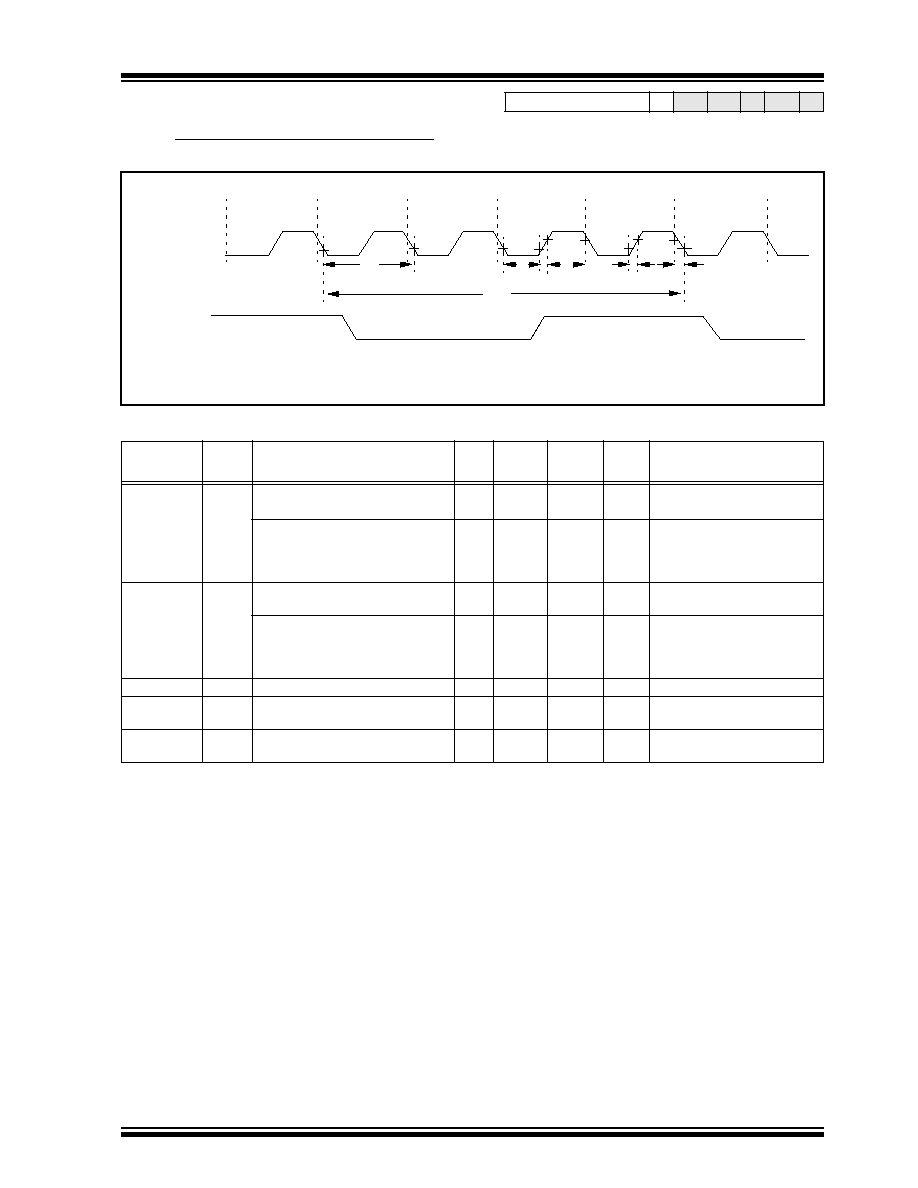
©
1996 Microchip Technology Inc.
DS30412C-page 155
PIC17C4X
Applicable Devices 42 R42 42A 43 R43 44
17.4
Timing Diagrams and Specifications
FIGURE 17-2: EXTERNAL CLOCK TIMING
TABLE 17-2:
EXTERNAL CLOCK TIMING REQUIREMENTS
Parameter
No.
Sym
Characteristic
Min
Typ
Max
Units
Conditions
Fosc
External CLKIN Frequency
(Note 1)
DC
DC
--
--
16
25
MHz
MHz
EC osc mode - PIC17C42-16
- PIC17C42-25
Oscillator Frequency
(Note 1)
DC
1
1
DC
--
--
--
--
4
16
25
2
MHz
MHz
MHz
MHz
RC osc mode
XT osc mode - PIC17C42-16
- PIC17C42-25
LF osc mode
1
Tosc
External CLKIN Period
(Note 1)
62.5
40
--
--
--
--
ns
ns
EC osc mode - PIC17C42-16
- PIC17C42-25
Oscillator Period
(Note 1)
250
62.5
40
500
--
--
--
--
--
1,000
1,000
--
ns
ns
ns
ns
RC osc mode
XT osc mode - PIC17C42-16
- PIC17C42-25
LF osc mode
2
T
CY
Instruction Cycle Time (Note 1)
160
4/Fosc
DC
ns
3
TosL,
TosH
Clock in (OSC1) High or Low Time
10
--
--
ns
EC oscillator
4
TosR,
TosF
Clock in (OSC1) Rise or Fall Time
--
--
5
ns
EC oscillator
Data in "Typ" column is at 5V, 25∞C unless otherwise stated. These parameters are for design guidance only and are not
tested.
These parameters are for design guidance only and are not tested, nor characterized.
Note 1:
Instruction cycle period (T
CY
) equals four times the input oscillator time-base period. All specified values are based on
characterization data for that particular oscillator type under standard operating conditions with the device executing code.
Exceeding these specified limits may result in unstable oscillator operation and/or higher than expected current consump-
tion. All devices are tested to operate at "min." values with an external clock applied to the OSC1 pin.
When an external clock input is used, the "Max." cycle time limit is "DC" (no clock) for all devices.
OSC1
OSC2
Q4
Q1
Q2
Q3
Q4
Q1
1
3
3
4
4
2
In EC and RC modes only.

PIC17C4X
DS30412C-page 156
©
1996 Microchip Technology Inc.
Applicable Devices 42 R42 42A 43 R43 44
FIGURE 17-3: CLKOUT AND I/O TIMING
TABLE 17-3:
CLKOUT AND I/O TIMING REQUIREMENTS
Parameter
No.
Sym
Characteristic
Min
Typ
Max
Units
Conditions
10
TosH2ckL
OSC1
to CLKOUT
--
15
30
ns
Note 1
11
TosH2ckH
OSC1
to CLKOUT
--
15
30
ns
Note 1
12
TckR
CLKOUT rise time
--
5
15
ns
Note 1
13
TckF
CLKOUT fall time
--
5
15
ns
Note 1
14
TckH2ioV
CLKOUT
to Port out valid
--
--
0.5T
CY
+ 20
ns
Note 1
15
TioV2ckH
Port in valid before CLKOUT
0.25T
CY
+ 25
--
--
ns
Note 1
16
TckH2ioI
Port in hold after CLKOUT
0
--
--
ns
Note 1
17
TosH2ioV
OSC1
(Q1 cycle) to Port out valid
--
--
100
ns
20
TioR
Port output rise time
--
10
35
ns
21
TioF
Port output fall time
--
10
35
ns
22
TinHL
INT pin high or low time
25 *
--
--
ns
23
TrbHL
RB7:RB0 change INT high or low time
25 *
--
--
ns
*
These parameters are characterized but not tested.
Data in "Typ" column is at 5V, 25∞C unless otherwise stated. These parameters are for design guidance only and are not
tested.
These parameters are for design guidance only and are not tested, nor characterized.
Note 1:
Measurements are taken in EC Mode where OSC2 output = 4 x T
OSC
= T
CY
.
OSC1
OSC2
I/O Pin
(input)
I/O Pin
(output)
Q4
Q1
Q2
Q3
10
13
14
17
20, 21
22
23
15
11
12
16
old value
new value
In EC and RC modes only.

©
1996 Microchip Technology Inc.
DS30412C-page 157
PIC17C4X
Applicable Devices 42 R42 42A 43 R43 44
FIGURE 17-4: RESET, WATCHDOG TIMER, OSCILLATOR START-UP TIMER AND POWER-UP
TIMER TIMING
TABLE 17-4:
RESET, WATCHDOG TIMER, OSCILLATOR START-UP TIMER AND POWER-UP
TIMER REQUIREMENTS
Parameter
No.
Sym
Characteristic
Min
Typ
Max
Units
Conditions
30
TmcL
MCLR Pulse Width (low)
100 *
--
--
ns
31
Twdt
Watchdog Timer Time-out Period
(Prescale = 1)
5 *
12
25 *
ms
32
Tost
Oscillation Start-up Timer Period
1024 T
OSC
ß
ms
T
OSC
= OSC1 period
33
Tpwrt
Power-up Timer Period
40 *
96
200 *
ms
35
TmcL2adI MCLR to System Interface bus
(AD15:AD0) invalid
--
--
100 *
ns
*
These parameters are characterized but not tested.
Data in "Typ" column is at 5V, 25∞C unless otherwise stated. These parameters are for design guidance only and are not
tested.
These parameters are for design guidance only and are not tested, nor characterized.
ß
This specification ensured by design.
V
DD
MCLR
Internal
POR
PWRT
Time-out
OSC
Time-out
Internal
RESET
Watchdog
Timer
RESET
33
32
30
31
Address /
Data
35

PIC17C4X
DS30412C-page 158
©
1996 Microchip Technology Inc.
Applicable Devices 42 R42 42A 43 R43 44
FIGURE 17-5: TIMER0 CLOCK TIMINGS
TABLE 17-5:
TIMER0 CLOCK REQUIREMENTS
FIGURE 17-6: TIMER1, TIMER2, AND TIMER3 CLOCK TIMINGS
TABLE 17-6:
TIMER1, TIMER2, AND TIMER3 CLOCK REQUIREMENTS
Parameter
No.
Sym Characteristic
Min
Typ Max Units Conditions
40
Tt0H T0CKI High Pulse Width
No Prescaler
0.5T
CY
+ 20 ß
--
--
ns
With Prescaler
10*
--
--
ns
41
Tt0L T0CKI Low Pulse Width
No Prescaler
0.5T
CY
+ 20 ß
--
--
ns
With Prescaler
10*
--
--
ns
42
Tt0P T0CKI Period
T
CY
+ 40 ß
N
--
--
ns
N = prescale value
(1, 2, 4, ..., 256)
*
These parameters are characterized but not tested.
Data in "Typ" column is at 5V, 25∞C unless otherwise stated. These parameters are for design guidance only and are not
tested.
ß
This specification ensured by design.
Parameter
No.
Sym
Characteristic
Min
Typ
Max
Units Conditions
45
Tt123H
TCLK12 and TCLK3 high time
0.5 T
CY
+ 20 ß
--
--
ns
46
Tt123L
TCLK12 and TCLK3 low time
0.5 T
CY
+ 20 ß
--
--
ns
47
Tt123P
TCLK12 and TCLK3 input period
T
CY
+ 40 ß
N
--
--
ns
N = prescale value
(1, 2, 4, 8)
48
TckE2tmrI Delay from selected External Clock Edge to
Timer increment
2T
OSC
ß
--
6 Tosc ß
--
*
These parameters are characterized but not tested.
Data in "Typ" column is at 5V, 25∞C unless otherwise stated. These parameters are for design guidance only and are not
tested.
ß
This specification ensured by design.
RA1/T0CKI
40
41
42
TCLK12
45
46
or
TCLK3
TMRx
48
48
47
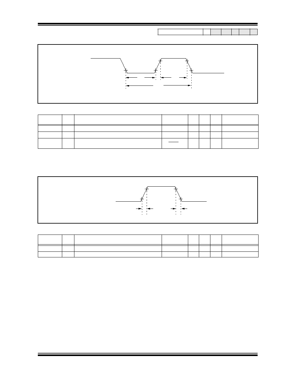
©
1996 Microchip Technology Inc.
DS30412C-page 159
PIC17C4X
Applicable Devices 42 R42 42A 43 R43 44
FIGURE 17-7: CAPTURE TIMINGS
TABLE 17-7:
CAPTURE REQUIREMENTS
FIGURE 17-8: PWM TIMINGS
TABLE 17-8:
PWM REQUIREMENTS
Parameter
No.
Sym Characteristic
Min
Typ Max Units Conditions
50
TccL Capture1 and Capture2 input low time
10 *
--
--
ns
51
TccH Capture1 and Capture2 input high time
10 *
--
--
ns
52
TccP Capture1 and Capture2 input period
2 T
CY
ß
N
--
--
ns
N = prescale value
(4 or 16)
*
These parameters are characterized but not tested.
Data in "Typ" column is at 5V, 25
∞
C unless otherwise stated. These parameters are for design guidance only and are not
tested.
ß
This specification ensured by design.
Parameter
No.
Sym Characteristic
Min
Typ Max Units Conditions
53
TccR PWM1 and PWM2 output rise time
--
10 * 35 *ß
ns
54
TccF PWM1 and PWM2 output fall time
--
10 * 35 *ß
ns
*
These parameters are characterized but not tested.
Data in "Typ" column is at 5V, 25
∞
C unless otherwise stated. These parameters are for design guidance only and are not
tested.
ß
This specification ensured by design.
CAP1
and CAP2
(Capture Mode)
50
51
52
PWM1
and PWM2
(PWM Mode)
53
54

PIC17C4X
DS30412C-page 160
©
1996 Microchip Technology Inc.
Applicable Devices 42 R42 42A 43 R43 44
FIGURE 17-9: USART MODULE: SYNCHRONOUS TRANSMISSION (MASTER/SLAVE) TIMING
TABLE 17-9:
SERIAL PORT SYNCHRONOUS TRANSMISSION REQUIREMENTS
FIGURE 17-10: USART MODULE: SYNCHRONOUS RECEIVE (MASTER/SLAVE) TIMING
TABLE 17-10: SERIAL PORT SYNCHRONOUS RECEIVE REQUIREMENTS
Parameter
No.
Sym
Characteristic
Min
Typ
Max
Units Conditions
120
TckH2dtV
SYNC XMIT (MASTER & SLAVE)
Clock high to data out valid
--
--
65
ns
121
TckRF
Clock out rise time and fall time (Master
Mode)
--
10
35
ns
122
TdtRF
Data out rise time and fall time
--
10
35
ns
Data in "Typ" column is at 5V, 25
∞
C unless otherwise stated. These parameters are for design guidance only and are not
tested.
Parameter
No.
Sym
Characteristic
Min
Typ
Max
Units Conditions
125
TdtV2ckL
SYNC RCV (MASTER & SLAVE)
Data hold before CK
(DT hold time)
15
--
--
ns
126
TckL2dtl
Data hold after CK
(DT hold time)
15
--
--
ns
Data in "Typ" column is at 5V, 25
∞
C unless otherwise stated. These parameters are for design guidance only and are not
tested.
121
121
120
122
RA5/TX/CK
RA4/RX/DT
pin
pin
125
126
RA5/TX/CK
RA4/RX/DT
pin
pin

©
1996 Microchip Technology Inc.
DS30412C-page 161
PIC17C4X
Applicable Devices 42 R42 42A 43 R43 44
FIGURE 17-11: MEMORY INTERFACE WRITE TIMING
TABLE 17-11: MEMORY INTERFACE WRITE REQUIREMENTS
Parameter
No.
Sym
Characteristic
Min
Typ
Max
Units Conditions
150
TadV2alL
AD<15:0> (address) valid to ALE
(address setup time)
0.25Tcy - 30
--
--
ns
151
TalL2adI
ALE
to address out invalid
(address hold time)
0
--
--
ns
152
TadV2wrL
Data out valid to WR
(data setup time)
0.25Tcy - 40
--
--
ns
153
TwrH2adI
WR
to data out invalid
(data hold time)
--
0.25T
CY
ß
--
ns
154
TwrL
WR pulse width
--
0.25T
CY
ß
--
ns
*
These parameters are characterized but not tested.
Data in "Typ" column is at 5V, 25
∞
C unless otherwise stated. These parameters are for design guidance only and are not
tested.
ß
This specification is guaranteed by design.
OSC1
ALE
OE
WR
AD<15:0>
Q1
Q2
Q3
Q4
Q1
Q2
150
151
152
153
154
addr out
data out
addr out
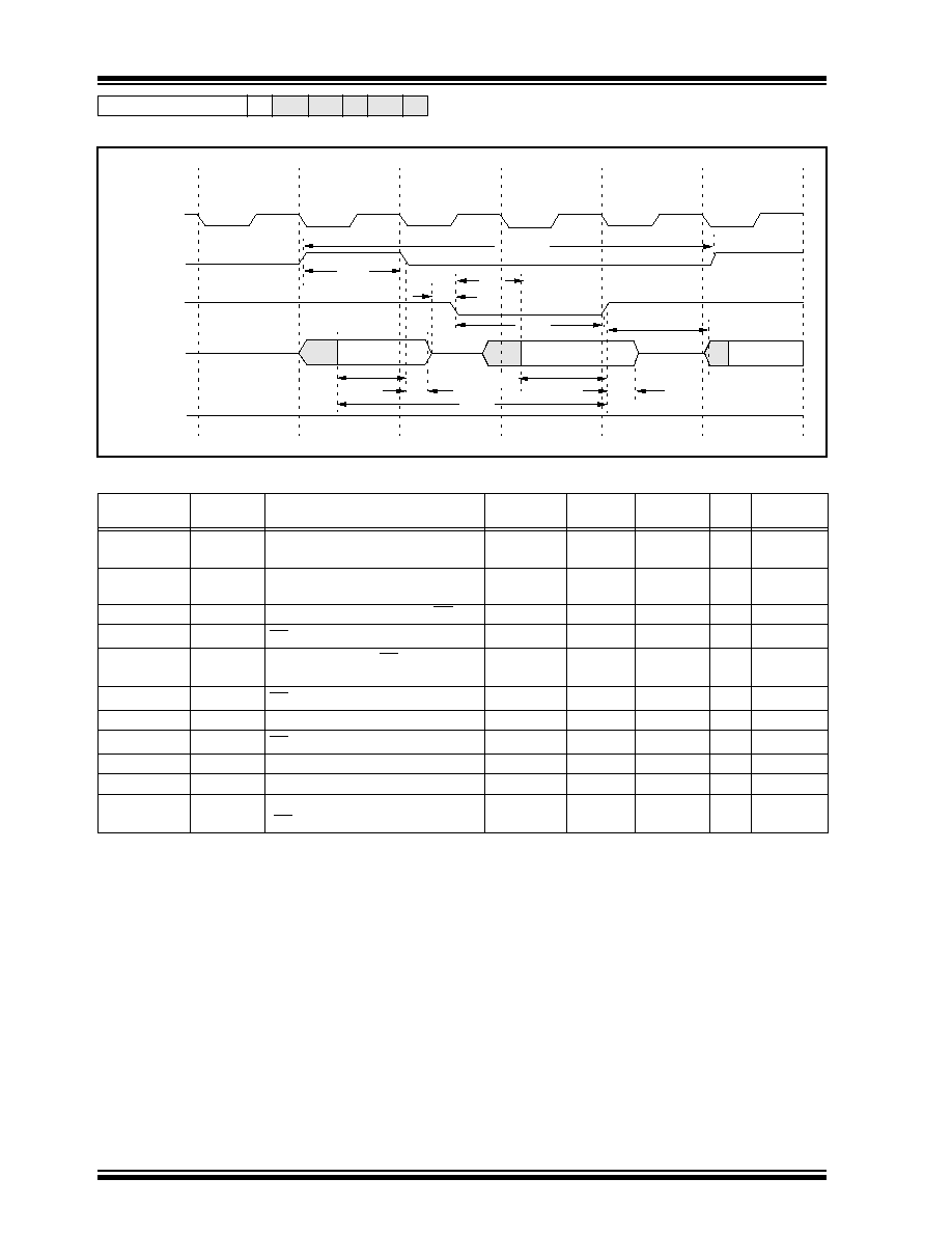
PIC17C4X
DS30412C-page 162
©
1996 Microchip Technology Inc.
Applicable Devices 42 R42 42A 43 R43 44
FIGURE 17-12: MEMORY INTERFACE READ TIMING
TABLE 17-12: MEMORY INTERFACE READ REQUIREMENTS
Parameter
No.
Sym
Characteristic
Min
Typ
Max
Units Conditions
150
TadV2alL
AD<15:0> (address) valid to ALE
(address setup time)
0.25Tcy - 30
--
--
ns
151
TalL2adI
ALE
to address out invalid
(address hold time)
5*
--
--
ns
160
TadZ2oeL
AD<15:0> high impedance to OE
0*
--
--
ns
161
ToeH2adD
OE
to AD<15:0> driven
0.25Tcy - 15
--
--
ns
162
TadV2oeH
Data in valid before OE
(data setup time)
35
--
--
ns
163
ToeH2adI
OE
to data in invalid (data hold time)
0
--
--
ns
164
TalH
ALE pulse width
--
0.25T
CY
ß
--
ns
165
ToeL
OE pulse width
0.5Tcy - 35 ß
--
--
ns
166
TalH2alH
ALE
to ALE
(cycle time)
--
T
CY
ß
--
ns
167
Tacc
Address access time
--
--
0.75 T
CY
-40
ns
168
Toe
Output enable access time
(OE low to Data Valid)
--
--
0.5 T
CY
- 60
ns
*
These parameters are characterized but not tested.
Data in "Typ" column is at 5V, 25
∞
C unless otherwise stated. These parameters are for design guidance only and are not
tested.
ß
This specification guaranteed by design.
OSC1
ALE
OE
AD<15:0>
WR
Q1
Q2
Q3
Data in
Addr out
150
151
160
166
165
163
161
'1'
'1'
Q4
Q1
Q2
Addr out
164
168
167
162
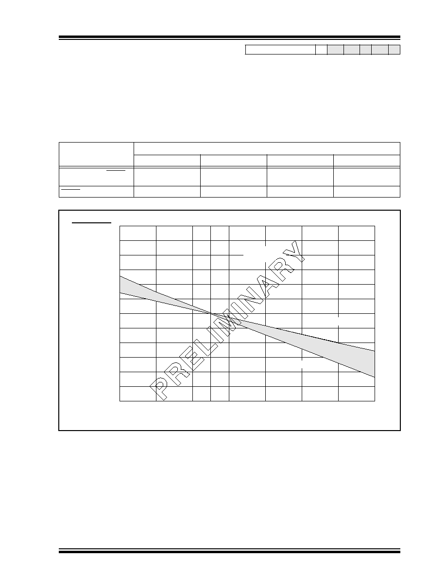
©
1996 Microchip Technology Inc.
DS30412C-page 163
PIC17C4X
Applicable Devices
42 R42 42A 43 R43 44
18.0
PIC17C42 DC AND AC CHARACTERISTICS
The graphs and tables provided in this section are for design guidance and are not tested or guaranteed. In some graphs
or tables the data presented are outside specified operating range (e.g. outside specified V
DD
range). This is for infor-
mation only and devices are ensured to operate properly only within the specified range.
The data presented in this section is a statistical summary of data collected on units from different lots over a period of
time. "Typical" represents the mean of the distribution while "max" or "min" represents (mean + 3
) and (mean - 3
)
respectively where
is standard deviation.
TABLE 18-1:
PIN CAPACITANCE PER PACKAGE TYPE
FIGURE 18-1: TYPICAL RC OSCILLATOR FREQUENCY vs. TEMPERATURE
Pin Name
Typical Capacitance (pF)
40-pin DIP
44-pin PLCC
44-pin MQFP
44-pin TQFP
All pins, except MCLR,
V
DD
, and V
SS
10
10
10
10
MCLR pin
20
20
20
20
F
OSC
F
OSC
(25
∞
C)
1.10
1.08
1.06
1.04
1.02
1.00
0.98
0.96
0.94
0.92
0.90
0
10
20
25
30
40
50
60
70
T(
∞
C)
Frequency normalized to +25
∞
C
V
DD
= 5.5V
V
DD
= 3.5V
Rext
10 k
Cext = 100 pF
This document was created with FrameMaker 4 0 4
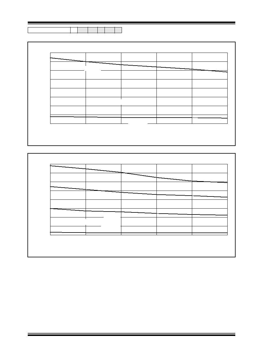
PIC17C4X
DS30412C-page 164
©
1996 Microchip Technology Inc.
Applicable Devices
42 R42 42A 43 R43 44
FIGURE 18-2: TYPICAL RC OSCILLATOR FREQUENCY vs. V
DD
FIGURE 18-3: TYPICAL RC OSCILLATOR FREQUENCY vs. V
DD
4.0
3.5
3.0
2.5
2.0
1.5
1.0
0.5
0.0
4.0
4.5
5.0
5.5
6.0
6.5
F
OSC
(MHz)
V
DD
(Volts)
R = 10k
Cext = 22 pF, T = 25
∞
C
R = 100k
4.0
3.5
3.0
2.5
2.0
1.5
1.0
0.5
0.0
4.0
4.5
5.0
5.5
6.0
6.5
F
OSC
(MHz)
V
DD
(Volts)
R = 10k
Cext = 100 pF, T = 25
∞
C
R = 100k
R = 3.3k
R = 5.1k

©
1996 Microchip Technology Inc.
DS30412C-page 165
PIC17C4X
Applicable Devices
42 R42 42A 43 R43 44
FIGURE 18-4: TYPICAL RC OSCILLATOR FREQUENCY vs. V
DD
TABLE 18-2:
RC OSCILLATOR FREQUENCIES
Cext
Rext
Average
Fosc @ 5V, 25
∞
C
22 pF
10k
3.33 MHz
±
12%
100k
353 kHz
±
13%
100 pF
3.3k
3.54 MHz
±
10%
5.1k
2.43 MHz
±
14%
10k
1.30 MHz
±
17%
100k
129 kHz
±
10%
300 pF
3.3k
1.54 MHz
±
14%
5.1k
980 kHz
±
12%
10k
564 kHz
±
16%
160k
35 kHz
±
18%
2.0
1.8
1.6
1.4
1.2
1.0
0.8
0.6
0.4
4.0
4.5
5.0
5.5
6.0
6.5
F
OSC
(MHz)
V
DD
(Volts)
R = 10k
Cext = 300 pF, T = 25
∞
C
R = 160k
R = 3.3k
R = 5.1k
0.2
0.0

PIC17C4X
DS30412C-page 166
©
1996 Microchip Technology Inc.
Applicable Devices
42 R42 42A 43 R43 44
FIGURE 18-5: TRANSCONDUCTANCE (gm) OF LF OSCILLATOR vs. V
DD
FIGURE 18-6: TRANSCONDUCTANCE (gm) OF XT OSCILLATOR vs. V
DD
500
450
400
350
300
250
200
150
100
2.5
3.0
3.5
4.0
4.5
5.0
gm(
µ
A/V)
V
DD
(Volts)
Min @ 85
∞
C
50
0
5.5
6.0
Max @ -40
∞
C
Typ @ 25
∞
C
20
18
16
14
12
10
8
6
4
2.5
3.0
3.5
4.0
4.5
5.0
gm(mA/V)
V
DD
(Volts)
Min @ 85
∞
C
2
0
5.5
6.0
Max @ -40
∞
C
Typ @ 25
∞
C

©
1996 Microchip Technology Inc.
DS30412C-page 167
PIC17C4X
Applicable Devices
42 R42 42A 43 R43 44
FIGURE 18-7: TYPICAL I
DD
vs. FREQUENCY (EXTERNAL CLOCK 25
∞
C)
FIGURE 18-8: MAXIMUM I
DD
vs. FREQUENCY (EXTERNAL CLOCK 125
∞
C TO -40
∞
C)
10k
100k
1M
10M
100M
100
1000
10000
100000
I
DD
(
µ
A)
External Clock Frequency (Hz)
7.0V
10
6.5V
6.0V
5.5V
4.5V
5.0V
4.0V
10k
100k
1M
10M
100M
100
1000
10000
100000
I
DD
(
µ
A)
External Clock Frequency (Hz)
6.5V
6.0V
5.5V
4.0V
4.5V
5.0V
7.0V
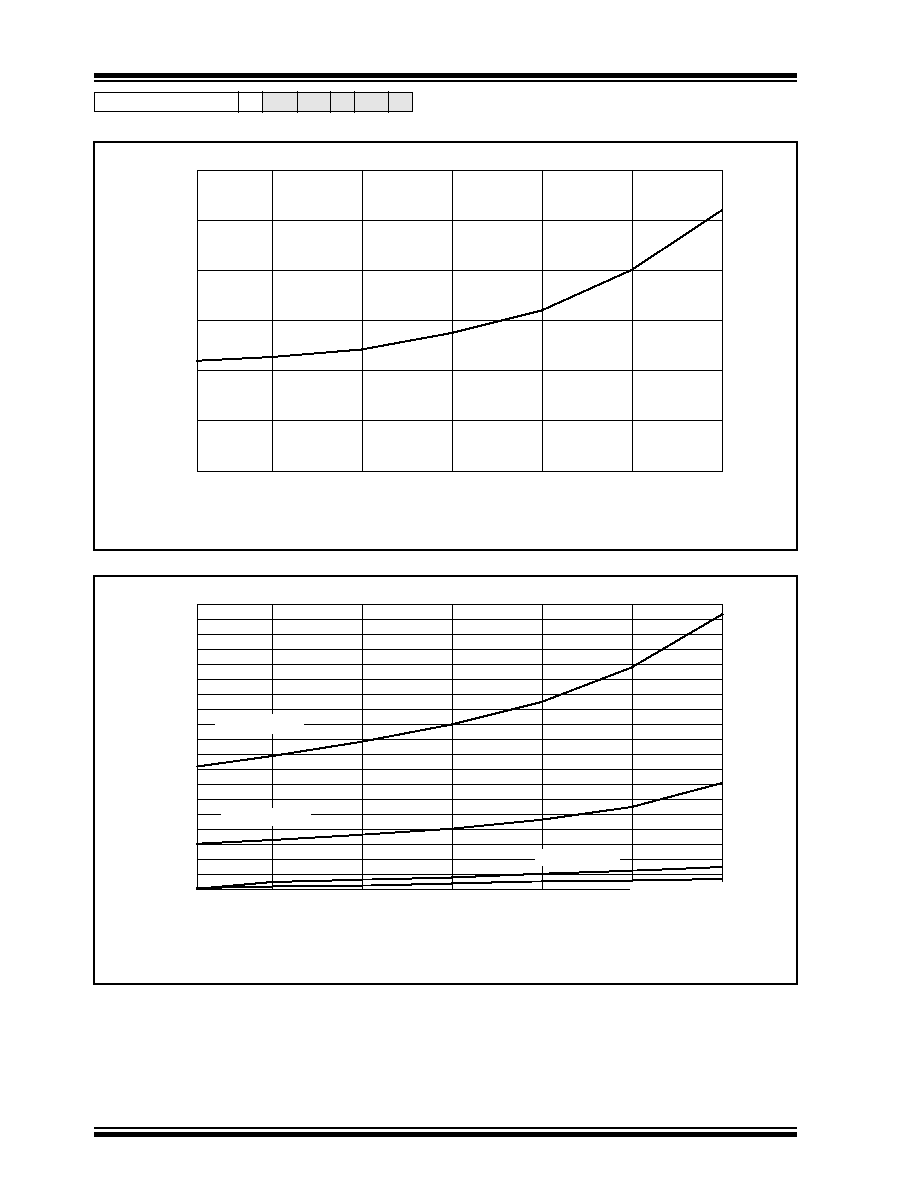
PIC17C4X
DS30412C-page 168
©
1996 Microchip Technology Inc.
Applicable Devices
42 R42 42A 43 R43 44
FIGURE 18-9: TYPICAL I
PD
vs. V
DD
WATCHDOG DISABLED 25
∞
C
FIGURE 18-10: MAXIMUM I
PD
vs. V
DD
WATCHDOG DISABLED
12
10
8
6
4
4.0
4.5
5.0
5.5
6.0
I
PD
(nA)
V
DD
(Volts)
2
0
6.5
7.0
600
500
400
300
200
4.0
4.5
5.0
5.5
6.0
I
PD
(nA)
V
DD
(Volts)
100
0
6.5
7.0
1300
1200
1100
1000
900
800
700
1900
1800
1700
1600
1500
1400
Temp. = 85
∞
C
Temp. = 70
∞
C
Temp. = 0
∞
C
Temp. = -40
∞
C

©
1996 Microchip Technology Inc.
DS30412C-page 169
PIC17C4X
Applicable Devices
42 R42 42A 43 R43 44
FIGURE 18-11: TYPICAL I
PD
vs. V
DD
WATCHDOG ENABLED 25
∞
C
FIGURE 18-12: MAXIMUM I
PD
vs. V
DD
WATCHDOG ENABLED
30
25
20
15
10
4.0
4.5
5.0
5.5
6.0
I
PD
(
µ
A)
V
DD
(Volts)
5
0
6.5
7.0
60
50
40
30
20
4.0
4.5
5.0
5.5
6.0
I
PD
(
µ
A)
V
DD
(Volts)
10
0
6.5
7.0
-40
∞
C
0
∞
C
70
∞
C
85
∞
C
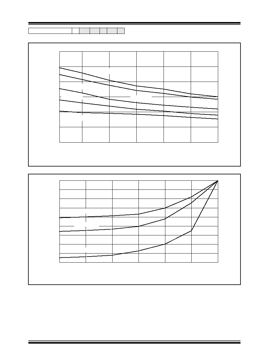
PIC17C4X
DS30412C-page 170
©
1996 Microchip Technology Inc.
Applicable Devices 42 R42 42A 43 R43 44
FIGURE 18-13: WDT TIMER TIME-OUT PERIOD vs. V
DD
FIGURE 18-14: I
OH
vs. V
OH
, V
DD
= 3V
30
25
20
15
10
4.0
4.5
5.0
5.5
6.0
V
DD
(Volts)
5
0
6.5
7.0
WDT P
e
r
iod (ms)
Max. 70
∞
C
Typ. 25
∞
C
Min. 0
∞
C
Min. -40
∞
C
Max. 85
∞
C
0
-2
-4
-6
-8
-10
-12
-14
0.0
0.5
1.0
1.5
2.0
2.5
I
OH
(mA)
V
DD
(Volts)
Min @ 85
∞
C
-16
-18
3.0
Max @ -40
∞
C
Typ @ 25
∞
C

©
1996 Microchip Technology Inc.
DS30412C-page 171
PIC17C4X
Applicable Devices 42 R42 42A 43 R43 44
FIGURE 18-15: I
OH
vs. V
OH
, V
DD
= 5V
FIGURE 18-16: I
OL
vs. V
OL
, V
DD
= 3V
0
-5
-10
-15
-20
-25
0.0
0.5
1.0
1.5
2.0
2.5
I
OH
(mA)
V
DD
(Volts)
-30
-35
3.0
Max @ -40
∞
C
Typ @ 25
∞
C
3.5
4.0
4.5
5.0
Min @ 85
∞
C
30
25
20
15
10
0.0
0.5
1.0
1.5
2.0
V
DD
(Volts)
5
0
2.5
3.0
I
OL
(mA)
Min. +85
∞
C
Typ. 25
∞
C
Max. -40
∞
C

PIC17C4X
DS30412C-page 172
©
1996 Microchip Technology Inc.
Applicable Devices 42 R42 42A 43 R43 44
FIGURE 18-17: I
OL
vs. V
OL
, V
DD
= 5V
FIGURE 18-18: V
TH
(INPUT THRESHOLD VOLTAGE) OF I/O PINS (TTL)
VS
. V
DD
90
80
70
60
50
40
30
20
0.0
0.5
1.0
1.5
2.0
2.5
I
OH
(mA)
V
DD
(Volts)
Min @ +85
∞
C
10
0
3.0
Max @ -40
∞
C
Typ @ 25
∞
C
Typ @ 25
∞
C
2.5
V
TH
(V
olts)
V
DD
(Volts)
0.6
Max (-40
∞
C to +85
∞
C)
3.0
3.5
4.0
4.5
5.0
5.5
6.0
0.8
1.0
1.2
1.4
1.6
1.8
2.0
Min (-40
∞
C to +85
∞
C)
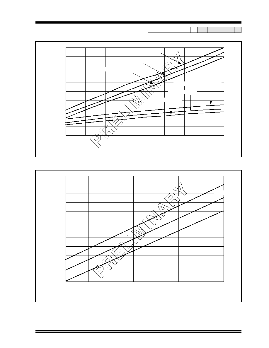
©
1996 Microchip Technology Inc.
DS30412C-page 173
PIC17C4X
Applicable Devices 42 R42 42A 43 R43 44
FIGURE 18-19: V
TH
, V
IL
of I/O PINS (SCHMITT TRIGGER)
VS
. V
DD
FIGURE 18-20: V
TH
(INPUT THRESHOLD VOLTAGE) OF OSC1 INPUT
(IN XT AND LF MODES) vs. V
DD
2.0
V
IH
, V
IL
(V
olts)
V
DD
(Volts)
0.0
2.5
3.0
3.5
4.0
4.5
5.0
5.5
0.5
1.0
1.5
2.0
2.5
3.0
3.5
6.0
4.0
4.5
5.0
V
IH
, max (-40
∞
C to +85
∞
C)
V
IH
, typ (25
∞
C)
V
IH
, min (-40
∞
C to +85
∞
C)
V
IL
, max (-40
∞
C to +85
∞
C)
V
IL
, typ (25
∞
C)
V
IL
, min (-40
∞
C to +85
∞
C)
V
TH
,(V
olts)
V
DD
(Volts)
1.0
2.5
3.0
3.5
4.0
4.5
5.0
5.5
1.2
1.4
1.6
1.8
2.0
2.2
2.4
6.0
2.6
2.8
3.0
Min (-40
∞
C to +85
∞
C)
3.2
3.4
Max (-40
∞
C to +85
∞
C)
Typ (25
∞
C)

PIC17C4X
DS30412C-page 174
©
1996 Microchip Technology Inc.
NOTES:

©
1996 Microchip Technology Inc.
DS30412C-page 175
PIC17C4X
Applicable Devices
42 R42 42A 43 R43 44
19.0
PIC17CR42/42A/43/R43/44 ELECTRICAL CHARACTERISTICS
Absolute Maximum Ratings
Ambient temperature under bias..................................................................................................................-55 to +125∞C
Storage temperature ............................................................................................................................... -65∞C to +150∞C
Voltage on V
DD
with respect to V
SS
................................................................................................................ 0 to +7.5V
Voltage on MCLR with respect to V
SS
(Note 2) ..........................................................................................-0.6V to +14V
Voltage on RA2 and RA3 with respect to V
SS
..............................................................................................-0.6V to +14V
Voltage on all other pins with respect to V
SS
..................................................................................... -0.6V to V
DD
+ 0.6V
Total power dissipation (Note 1).................................................................................................................................1.0W
Maximum current out of V
SS
pin(s) - total ..............................................................................................................250 mA
Maximum current into V
DD
pin(s) - total .................................................................................................................200 mA
Input clamp current, I
IK
(V
I
< 0 or V
I
> V
DD
)
......................................................................................................................±
20 mA
Output clamp current, I
OK
(V
O
< 0 or V
O
> V
DD
)
...............................................................................................................±
20 mA
Maximum output current sunk by any I/O pin (except RA2 and RA3)......................................................................35 mA
Maximum output current sunk by RA2 or RA3 pins .................................................................................................60 mA
Maximum output current sourced by any I/O pin .....................................................................................................20 mA
Maximum current sunk by
PORTA and PORTB (combined) ..................................................................................150 mA
Maximum current sourced by PORTA and PORTB (combined).............................................................................100 mA
Maximum current sunk by PORTC, PORTD and PORTE (combined)...................................................................150 mA
Maximum current sourced by PORTC, PORTD and PORTE (combined)..............................................................100 mA
Note 1:
Power dissipation is calculated as follows: Pdis = V
DD
x {I
DD
-
I
OH
} +
{(V
DD
-V
OH
) x I
OH
} +
(V
OL
x I
OL
)
Note 2:
Voltage spikes below V
SS
at the MCLR pin, inducing currents greater than 80 mA, may cause latch-up.
Thus, a series resistor of 50-100
should be used when applying a "low" level to the MCLR pin rather than
pulling this pin directly to V
SS
.
NOTICE: Stresses above those listed under "Absolute Maximum Ratings" may cause permanent damage to the
device. This is a stress rating only and functional operation of the device at those or any other conditions above
those indicated in the operation listings of this specification is not implied. Exposure to maximum rating conditions for
extended periods may affect device reliability.
This document was created with FrameMaker 4 0 4
PIC17C4X
DS30412C-page 176
©
1996 Microchip Technology Inc.
Applicable Devices
42 R42 42A 43 R43 44
TABLE 19-1:
CROSS REFERENCE OF DEVICE SPECS FOR OSCILLATOR CONFIGURATIONS
AND FREQUENCIES OF OPERATION (COMMERCIAL DEVICES)
OSC
PIC17LCR42-08
PIC17LC42A-08
PIC17LC43-08
PIC17LCR43-08
PIC17LC44-08
PIC17CR42-16
PIC17C42A-16
PIC17C43-16
PIC17CR43-16
PIC17C44-16
PIC17CR42-25
PIC17C42A-25
PIC17C43-25
PIC17CR43-25
PIC17C44-25
PIC17CR42-33
PIC17C42A-33
PIC17C43-33
PIC17CR43-33
PIC17C44-33
JW De
vices
(Ceramic
Windo
wed
De
vices)
RC
V
DD
:
2.5V to 6.0V
I
DD
:
6
mA
max.
I
PD
: 5
µ
A max.
at 5.5V
WDT dis
ab
led
F
req:
4 MHz max.
V
DD
:
4.5V to 6.0V
I
DD
:
6
mA
max.
I
PD
: 5
µ
A max.
at 5.5V
WDT dis
ab
led
F
req:
4 MHz max.
V
DD
:
4.5V to 6.0V
I
DD
:
6
mA
max.
I
PD
: 5
µ
A max.
at 5.5V
WDT dis
ab
led
F
req:
4 MHz max.
V
DD
:
4.5V to 6.0V
I
DD
:
6
mA
max.
I
PD
: 5
µ
A max.
at 5.5V
WDT dis
ab
led
F
req:
4 MHz max.
V
DD
:
4.5V to 6.0V
I
DD
:
6
mA
max.
I
PD
: 5
µ
A max.
at 5.5V
WDT dis
ab
led
F
req:
4 MHz max.
XT
V
DD
:
2.5V to 6.0V
I
DD
:
12
mA
max.
I
PD
: 5
µ
A max.
at 5.5V
WDT dis
ab
led
F
req:
8 MHz max.
V
DD
:
4.5V to 6.0V
I
DD
:
24
mA
max.
I
PD
: 5
µ
A max.
at 5.5V
WDT dis
ab
led
F
req:
16 MHz max.
V
DD
:
4.5V to 6.0V
I
DD
:
38
mA
max.
I
PD
: 5
µ
A max.
at 5.5V
WDT dis
ab
led
F
req:
25 MHz max.
V
DD
:
4.5V to 6.0V
I
DD
:
38
mA
max.
I
PD
: 5
µ
A max.
at 5.5V
WDT dis
ab
led
F
req:
33 MHz max.
V
DD
:
4.5V to 6.0V
I
DD
:
38
mA
max.
I
PD
: 5
µ
A max.
at 5.5V
WDT dis
ab
led
F
req:
33 MHz max.
EC
V
DD
:
2.5V to 6.0V
I
DD
:
12
mA
max.
I
PD
: 5
µ
A max.
at 5.5V
WDT disab
led
F
req:
8 MHz max.
V
DD
:
4.5V to 6.0V
I
DD
:
24
mA
max.
I
PD
: 5
µ
A max.
at 5.5V
WDT dis
ab
led
F
req:
16 MHz Max
V
DD
:
4.5V to 6.0V
I
DD
:
38
mA
max.
I
PD
: 5
µ
A max.
at 5.5V
WDT disab
led
F
req:
25 MHz max.
V
DD
:
4.5V to 6.0V
I
DD
:
38
mA
max.
I
PD
: 5
µ
A max.
at 5.5V
WDT disab
led
F
req:
33 MHz max.
V
DD
:
4.5V to 6.0V
I
DD
:
38
mA
max.
I
PD
: 5
µ
A max.
at 5.5V
WDT disab
led
F
req:
33 MHz max.
LF
V
DD
:
2.5V to 6.0V
I
DD
:
150
µ
A max.
at 32 kHz
I
PD
: 5
µ
A max.
at 5.5V
WDT dis
ab
led
F
req:
2 MHz max.
V
DD
:
4.5V to 6.0V
I
DD
:
95
µ
A typ
.
at 32 kHz
I
PD
:
< 1
µ
A typ
.
at 5.5V
WDT dis
ab
led
F
req:
2 MHz max.
V
DD
:
4.5V to 6.0V
I
DD
:
95
µ
A typ
.
at 32 kHz
I
PD
:
< 1
µ
A typ
.
at 5.5V
WDT dis
ab
led
F
req:
2 MHz max.
V
DD
:
4.5V to 6.0V
I
DD
:
95
µ
A typ
.
at 32 kHz
I
PD
:
< 1
µ
A typ
.
at 5.5V
WDT dis
ab
led
F
req:
2 MHz max.
V
DD
:
2.5V to 6.0V
I
DD
:
150
µ
A max.
at 32 kHz
I
PD
: 5
µ
A max.
at 5.5V
WDT dis
ab
led
F
req:
2 MHz max.
The shaded sections indicate oscillator selections which are tested f
or functionality
, b
ut not f
or MIN/MAX specifi
cations
.
It is recommended that the user
select the de
vice type that
ensures t
he specifi
cations required.

©
1996 Microchip Technology Inc.
DS30412C-page 177
PIC17C4X
Applicable Devices 42 R42 42A 43 R43 44
19.1
DC CHARACTERISTICS:
PIC17CR42/42A/43/R43/44-16 (Commercial, Industrial)
PIC17CR42/42A/43/R43/44-25 (Commercial, Industrial)
PIC17CR42/42A/43/R43/44-33 (Commercial, Industrial)
DC CHARACTERISTICS
Standard Operating Conditions (unless otherwise stated)
Operating temperature
-40∞C
T
A
+85∞C for industrial and
0∞C
T
A
+70∞C for commercial
Parameter
No.
Sym
Characteristic
Min
Typ
Max
Units
Conditions
D001
V
DD
Supply Voltage
4.5
≠
6.0
V
D002
V
DR
RAM Data Retention
Voltage (Note 1)
1.5 *
≠
≠
V
Device in SLEEP mode
D003
V
POR
V
DD
start voltage to
ensure internal
Power-on Reset signal
≠
V
SS
≠
V
See section on Power-on Reset for
details
D004
S
VDD
V
DD
rise rate to
ensure internal
Power-on Reset signal
0.060 *
≠
≠
mV/ms See section on Power-on Reset for
details
D010
D011
D012
D013
D015
D014
I
DD
Supply Current
(Note 2)
≠
≠
≠
≠
≠
≠
3
6
11
19
25
95
6
12 *
24 *
38
50
150
mA
mA
mA
mA
mA
µ
A
F
OSC
= 4 MHz (Note 4)
F
OSC
= 8 MHz
F
OSC
= 16 MHz
F
OSC
= 25 MHz
F
OSC
= 33 MHz
F
OSC
= 32 kHz,
WDT enabled (EC osc configuration)
D020
D021
I
PD
Power-down
Current (Note 3)
≠
≠
10
< 1
40
5
µ
A
µ
A
V
DD
= 5.5V, WDT enabled
V
DD
= 5.5V, WDT disabled
*
These parameters are characterized but not tested.
Data in "Typ" column is at 5V, 25∞C unless otherwise stated. These parameters are for design guidance only
and are not tested.
Note 1: This is the limit to which V
DD
can be lowered in SLEEP mode without losing RAM data.
2: The supply current is mainly a function of the operating voltage and frequency. Other factors such as I/O pin
loading and switching rate, oscillator type, internal code execution pattern, and temperature also have an
impact on the current consumption.
The test conditions for all I
DD
measurements in active operation mode are:
OSC1 = external square wave, from rail to rail; all I/O pins tristated, pulled to V
DD
or V
SS
, T0CKI = V
DD
,
MCLR = V
DD
; WDT enabled/disabled as specified.
Current consumed from the oscillator and I/O's driving external capacitive or resistive loads needs to be con-
sidered.
For the RC oscillator, the current through the external pull-up resistor (R) can be estimated as: V
DD
/ (2
∑
R).
For capacitive loads, the current can be estimated (for an individual I/O pin) as (C
L
∑
V
DD
)
∑
f
C
L
= Total capacitive load on the I/O pin; f = average frequency the I/O pin switches.
The capacitive currents are most significant when the device is configured for external execution (includes
extended microcontroller mode).
3: The power down current in SLEEP mode does not depend on the oscillator type. Power-down current is mea-
sured with the part in SLEEP mode, with all I/O pins in hi-impedance state and tied to V
DD
and V
SS
.
4: For RC osc configuration, current through Rext is not included. The current through the resistor can be esti-
mated by the formula I
R
= V
DD
/2Rext (mA) with Rext in kOhm.

PIC17C4X
DS30412C-page 178
©
1996 Microchip Technology Inc.
Applicable Devices 42 R42 42A 43 R43 44
19.2
DC CHARACTERISTICS:
PIC17LC42A/43/LC44 (Commercial, Industrial)
PIC17LCR42/43 (Commercial, Industrial)
DC CHARACTERISTICS
Standard Operating Conditions (unless otherwise stated)
Operating temperature
-40∞C
T
A
+85∞C for industrial and
0∞C
T
A
+70∞C for commercial
Parameter
No.
Sym
Characteristic
Min
Typ
Max
Units
Conditions
D001
V
DD
Supply Voltage
2.5
≠
6.0
V
D002
V
DR
RAM Data Retention
Voltage (Note 1)
1.5 *
≠
≠
V
Device in SLEEP mode
D003
V
POR
V
DD
start voltage to
ensure internal
Power-on Reset signal
≠
V
SS
≠
V
See section on Power-on Reset for
details
D004
S
VDD
V
DD
rise rate to
ensure internal
Power-on Reset signal
0.060 *
≠
≠
mV/ms See section on Power-on Reset for
details
D010
D011
D014
I
DD
Supply Current
(Note 2)
≠
≠
≠
3
6
95
6
12 *
150
mA
mA
µ
A
F
OSC
= 4 MHz (Note 4)
F
OSC
= 8 MHz
F
OSC
= 32 kHz,
WDT disabled (EC osc configuration)
D020
D021
I
PD
Power-down
Current (Note 3)
≠
≠
10
< 1
40
5
µ
A
µ
A
V
DD
= 5.5V, WDT enabled
V
DD
= 5.5V, WDT disabled
*
These parameters are characterized but not tested.
Data in "Typ" column is at 5V, 25∞C unless otherwise stated. These parameters are for design guidance only
and are not tested.
Note 1: This is the limit to which V
DD
can be lowered in SLEEP mode without losing RAM data.
2: The supply current is mainly a function of the operating voltage and frequency. Other factors such as I/O pin
loading and switching rate, oscillator type, internal code execution pattern, and temperature also have an
impact on the current consumption.
The test conditions for all I
DD
measurements in active operation mode are:
OSC1=external square wave, from rail to rail; all I/O pins tristated, pulled to V
DD
or V
SS
, T0CKI = V
DD
, MCLR
= V
DD
; WDT enabled/disabled as specified.
Current consumed from the oscillator and I/O's driving external capacitive or resistive loads needs to be con-
sidered.
For the RC oscillator, the current through the external pull-up resistor (R) can be estimated as: V
DD
/ (2
∑
R).
For capacitive loads, the current can be estimated (for an individual I/O pin) as (C
L
∑
V
DD
)
∑
f
C
L
= Total capacitive load on the I/O pin; f = average frequency the I/O pin switches.
The capacitive currents are most significant when the device is configured for external execution (includes
extended microcontroller mode).
3: The power down current in SLEEP mode does not depend on the oscillator type. Power-down current is
measured with the part in SLEEP mode, with all I/O pins in hi-impedance state and tied to V
DD
or V
SS
.
4: For RC osc configuration, current through Rext is not included. The current through the resistor can be esti-
mated by the formula I
R
= V
DD
/2Rext (mA) with Rext in kOhm.

©
1996 Microchip Technology Inc.
DS30412C-page 179
PIC17C4X
Applicable Devices 42 R42 42A 43 R43 44
19.3
DC CHARACTERISTICS:
PIC17CR42/42A/43/R43/44-16 (Commercial, Industrial)
PIC17CR42/42A/43/R43/44-25 (Commercial, Industrial)
PIC17CR42/42A/43/R43/44-33 (Commercial, Industrial)
PIC17LCR42/42A/43/R43/44-08 (Commercial, Industrial)
DC CHARACTERISTICS
Standard Operating Conditions (unless otherwise stated)
Operating temperature
-40∞C
T
A
+85∞C for industrial and
0∞C
T
A
+70∞C for commercial
Operating voltage V
DD
range as described in Section 19.1
Parameter
No.
Sym
Characteristic
Min
Typ
Max
Units
Conditions
Input Low Voltage
V
IL
I/O ports
D030
with TTL buffer
V
SS
V
SS
≠
≠
0.8
0.2V
DD
V
V
4.5V
V
DD
5.5V
2.5V
V
DD
4.5V
D031
with Schmitt Trigger buffer
V
SS
≠
0.2V
DD
V
D032
MCLR, OSC1 (in EC and RC
mode)
Vss
≠
0.2V
DD
V
Note1
D033
OSC1 (in XT, and LF mode)
≠
0.5V
DD
≠
V
Input High Voltage
V
IH
I/O ports
D040
with TTL buffer
2.0
1 + 0.2V
DD
≠
≠
V
DD
V
DD
V
V
4.5V
V
DD
5.5V
2.5V
V
DD
4.5V
D041
with Schmitt Trigger buffer
0.8V
DD
≠
V
DD
V
D042
MCLR
0.8V
DD
≠
V
DD
V
Note1
D043
OSC1 (XT, and LF mode)
≠
0.5V
DD
≠
V
D050
V
HYS
Hysteresis of
Schmitt Trigger inputs
0.15V
DD
*
≠
≠
V
Input Leakage Current
(Notes 2, 3)
D060
I
IL
I/O ports (except RA2, RA3)
≠
≠
±
1
µ
A Vss
V
PIN
V
DD
,
I/O Pin at hi-impedance
PORTB weak pull-ups
disabled
D061
MCLR
≠
≠
±
2
µ
A V
PIN
=
Vss or
V
PIN
=
V
DD
D062
RA2, RA3
±
2
µ
A Vss
V
RA
2, V
RA
3
12V
D063
OSC1, TEST (EC, RC modes)
≠
≠
±
1
µ
A Vss
V
PIN
V
DD
D063B
OSC1, TEST (XT, LF modes)
≠
≠
V
PIN
µ
A R
F
1 M
, see Figure 14.2
D064
MCLR
≠
≠
10
µ
A V
MCLR
= V
PP
= 12V
(when not programming)
D070
I
PURB
PORTB weak pull-up current
60
200
400
µ
A V
PIN
= V
SS
, RBPU = 0
4.5V
V
DD
6.0V
*
These parameters are characterized but not tested.
Data in "Typ" column is at 5V, 25
∞
C unless otherwise stated. These parameters are for design guidance only
and are not tested.
These parameters are for design guidance only and are not tested, nor characterized.
Note 1: In RC oscillator configuration, the OSC1/CLKIN pin is a Schmitt Trigger input. It is not recommended that the
PIC17CXX devices be driven with external clock in RC mode.
2: The leakage current on the MCLR pin is strongly dependent on the applied voltage level. The specified levels
represent normal operating conditions. Higher leakage current may be measured at different input voltages.
3: Negative current is defined as coming out of the pin.
4: These specifications are for the programming of the on-chip program memory EPROM through the use of the
table write instructions. The complete programming specifications can be found in: PIC17CXX Programming
Specifications (Literature number DS30139).
5: The MCLR/V
PP
pin may be kept in this range at times other than programming, but is not recommended.
6: For TTL buffers, the better of the two specifications may be used.

PIC17C4X
DS30412C-page 180
©
1996 Microchip Technology Inc.
Applicable Devices 42 R42 42A 43 R43 44
Output Low Voltage
D080
D081
V
OL
I/O ports (except RA2 and RA3)
with TTL buffer
≠
≠
≠
≠
≠
≠
0.1V
DD
0.1V
DD
*
0.4
V
V
V
I
OL
= V
DD
/1.250 mA
4.5V
V
DD
6.0V
V
DD
=
2.5V
I
OL
= 6 mA, V
DD
= 4.5V
Note 6
D082
RA2 and RA3
≠
≠
3.0
V
I
OL
= 60.0 mA, V
DD
= 6.0V
D083
D084
OSC2/CLKOUT
(RC and EC osc modes)
≠
≠
≠
≠
0.4
0.1V
DD
*
V
V
I
OL
= 1 mA, V
DD
= 4.5V
I
OL
= V
DD
/5 mA
(PIC17LC43/LC44 only)
Output High Voltage (Note 3)
D090
D091
V
OH
I/O ports (except RA2 and RA3)
with TTL buffer
0.9V
DD
0.9V
DD
*
2.4
≠
≠
≠
≠
≠
≠
V
V
V
I
OH
= -V
DD
/2.500 mA
4.5V
V
DD
6.0V
V
DD
=
2.5V
I
OH
= -6.0 mA, V
DD
=4.5V
Note 6
D092
RA2 and RA3
≠
≠
12
V
Pulled-up to externally
applied voltage
D093
D094
OSC2/CLKOUT
(RC and EC osc modes)
2.4
0.9V
DD
*
≠
≠
≠
≠
V
V
I
OH
= -5 mA, V
DD
= 4.5V
I
OH
= -V
DD
/5 mA
(PIC17LC43/LC44 only)
Capacitive Loading Specs
on Output Pins
D100
C
OSC2
OSC2/CLKOUT pin
≠
≠
25
pF
In EC or RC osc modes
when OSC2 pin is outputting
CLKOUT.
external clock is used to
drive OSC1.
D101
C
IO
All I/O pins and OSC2
(in RC mode)
≠
≠
50 pF
D102
C
AD
System Interface Bus
(PORTC, PORTD and PORTE)
≠
≠
50
pF
In Microprocessor or
Extended Microcontroller
mode
DC CHARACTERISTICS
Standard Operating Conditions (unless otherwise stated)
Operating temperature
-40∞C
T
A
+85∞C for industrial and
0∞C
T
A
+70∞C for commercial
Operating voltage V
DD
range as described in Section 19.1
Parameter
No.
Sym
Characteristic
Min
Typ
Max
Units
Conditions
*
These parameters are characterized but not tested.
Data in "Typ" column is at 5V, 25
∞
C unless otherwise stated. These parameters are for design guidance only
and are not tested.
These parameters are for design guidance only and are not tested, nor characterized.
Note 1: In RC oscillator configuration, the OSC1/CLKIN pin is a Schmitt Trigger input. It is not recommended that the
PIC17CXX devices be driven with external clock in RC mode.
2: The leakage current on the MCLR pin is strongly dependent on the applied voltage level. The specified levels
represent normal operating conditions. Higher leakage current may be measured at different input voltages.
3: Negative current is defined as coming out of the pin.
4: These specifications are for the programming of the on-chip program memory EPROM through the use of the
table write instructions. The complete programming specifications can be found in: PIC17CXX Programming
Specifications (Literature number DS30139).
5: The MCLR/V
PP
pin may be kept in this range at times other than programming, but is not recommended.
6: For TTL buffers, the better of the two specifications may be used.
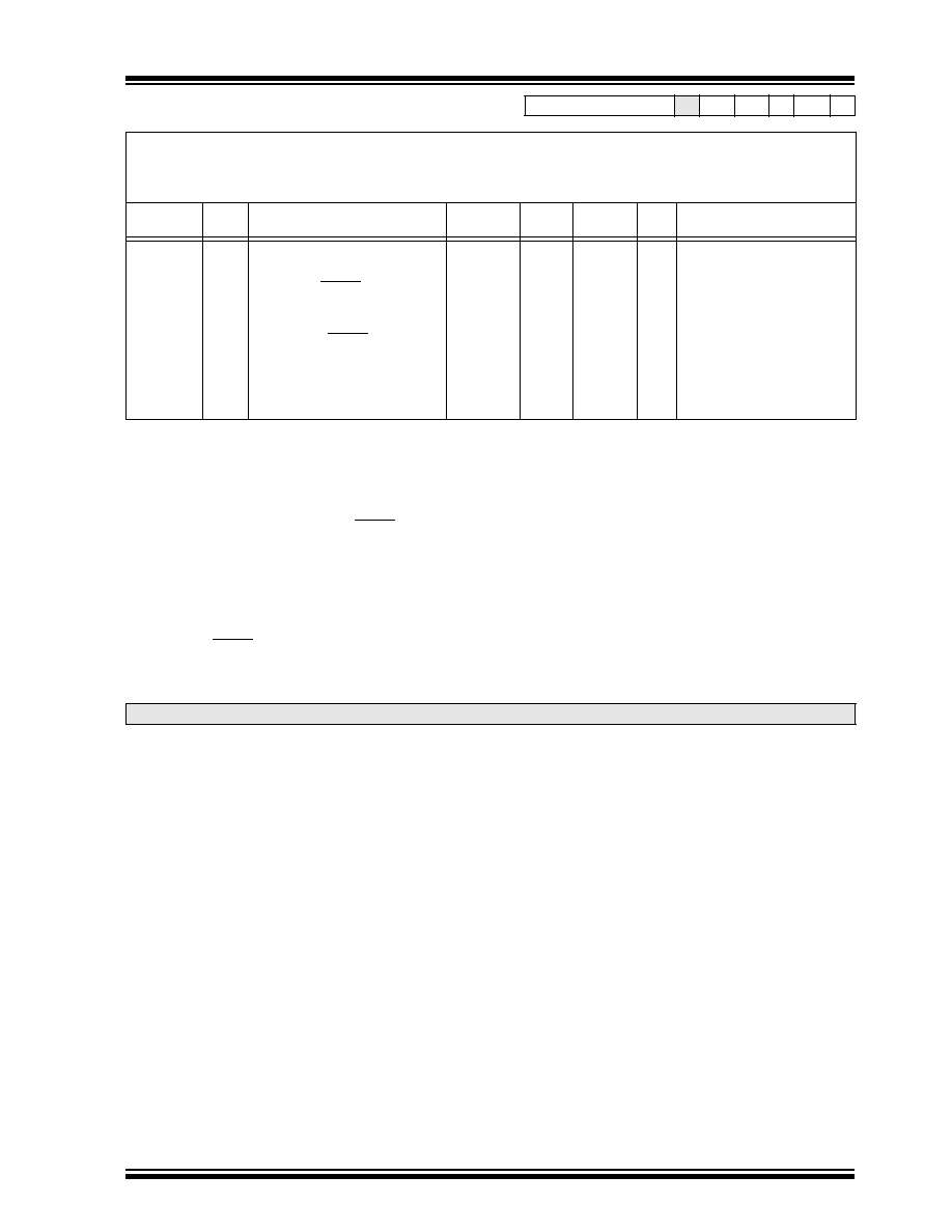
©
1996 Microchip Technology Inc.
DS30412C-page 181
PIC17C4X
Applicable Devices 42 R42 42A 43 R43 44
DC CHARACTERISTICS
Standard Operating Conditions (unless otherwise stated)
Operating temperature
-40∞C
T
A
+40∞C
Operating voltage V
DD
range as described in Section 19.1
Parameter
No.
Sym
Characteristic
Min
Typ
Max
Units
Conditions
Internal Program Memory
Programming Specs (Note 4)
D110
D111
D112
D113
D114
V
PP
V
DDP
I
PP
I
DDP
T
PROG
Voltage on MCLR/V
PP
pin
Supply voltage during
programming
Current into MCLR/V
PP
pin
Supply current during
programming
Programming pulse width
12.75
4.75
≠
≠
10
≠
5.0
25
≠
100
13.25
5.25
50
30
1000
V
V
mA
mA
µ
s
Note 5
Terminated via internal/
external interrupt or a reset
*
These parameters are characterized but not tested.
Data in "Typ" column is at 5V, 25
∞
C unless otherwise stated. These parameters are for design guidance only
and are not tested.
These parameters are for design guidance only and are not tested, nor characterized.
Note 1: In RC oscillator configuration, the OSC1/CLKIN pin is a Schmitt Trigger input. It is not recommended that the
PIC17CXX devices be driven with external clock in RC mode.
2: The leakage current on the MCLR pin is strongly dependent on the applied voltage level. The specified lev-
els represent normal operating conditions. Higher leakage current may be measured at different input volt-
ages.
3: Negative current is defined as coming out of the pin.
4: These specifications are for the programming of the on-chip program memory EPROM through the use of the
table write instructions. The complete programming specifications can be found in: PIC17CXX Programming
Specifications (Literature number DS30139).
5: The MCLR/V
PP
pin may be kept in this range at times other than programming, but is not recommended.
6: For TTL buffers, the better of the two specifications may be used.
Note:
When using the Table Write for internal programming, the device temperature must be less than 40∞C.

PIC17C4X
DS30412C-page 182
©
1996 Microchip Technology Inc.
Applicable Devices 42 R42 42A 43 R43 44
19.4
Timing Parameter Symbology
The timing parameter symbols have been created following one of the following formats:
1. TppS2ppS
3. T
CC
:
ST
(I
2
C specifications only)
2. TppS
4. Ts
(I
2
C specifications only)
T
F
Frequency
T
Time
Lowercase symbols (pp) and their meanings:
pp
ad
Address/Data
ost
Oscillator Start-Up Timer
al
ALE
pwrt
Power-Up Timer
cc
Capture1 and Capture2
rb
PORTB
ck
CLKOUT or clock
rd
RD
dt
Data in
rw
RD or WR
in
INT pin
t0
T0CKI
io
I/O port
t123
TCLK12 and TCLK3
mc
MCLR
wdt
Watchdog Timer
oe
OE wr
WR
os
OSC1
Uppercase symbols and their meanings:
S
D
Driven
L
Low
E
Edge
P
Period
F
Fall
R
Rise
H
High
V
Valid
I
Invalid (Hi-impedance)
Z
Hi-impedance

©
1996 Microchip Technology Inc.
DS30412C-page 183
PIC17C4X
Applicable Devices 42 R42 42A 43 R43 44
FIGURE 19-1: PARAMETER MEASUREMENT INFORMATION
All timings are measure between high and low measurement points as indicated in the figures below.
0.9 V
DD
0.1 V
DD
Rise Time
Fall Time
V
OH
= 0.7V
DD
V
DD
/2
V
OL
= 0.3V
DD
Data out valid
Data out invalid
Output
hi-impedance
Output
driven
0.25V
0.25V
0.25V
0.25V
OUTPUT LEVEL CONDITIONS
PORTC, D and E pins
All other input pins
V
IH
= 2.4V
V
IL
= 0.4V
Data in valid
Data in invalid
V
IH
= 0.9V
DD
V
IL
= 0.1V
DD
Data in valid
Data in invalid
INPUT LEVEL CONDITIONS
LOAD CONDITIONS
Load Condition 1
Pin
C
L
V
SS
50 pF
C
L

PIC17C4X
DS30412C-page 184
©
1996 Microchip Technology Inc.
Applicable Devices 42 R42 42A 43 R43 44
19.5
Timing Diagrams and Specifications
FIGURE 19-2: EXTERNAL CLOCK TIMING
TABLE 19-2:
EXTERNAL CLOCK TIMING REQUIREMENTS
Param
No.
Sym
Characteristic
Min
Typ
Max
Units
Conditions
Fosc
External CLKIN Frequency
(Note 1)
DC
DC
DC
DC
--
--
--
--
8
16
25
33
MHz
MHz
MHz
MHz
EC osc mode - 08 devices (8 MHz devices)
- 16 devices (16 MHz devices)
- 25 devices (25 MHz devices)
- 33 devices (33 MHz devices)
Oscillator Frequency
(Note 1)
DC
1
1
1
1
DC
--
--
--
--
--
--
4
8
16
25
33
2
MHz
MHz
MHz
MHz
MHz
MHz
RC osc mode
XT osc mode - 08 devices (8 MHz devices)
- 16 devices (16 MHz devices)
- 25 devices (25 MHz devices)
- 33 devices (33 MHz devices)
LF osc mode
1
Tosc
External CLKIN Period
(Note 1)
125
62.5
40
30.3
--
--
--
--
--
--
--
--
ns
ns
ns
ns
EC osc mode - 08 devices (8 MHz devices)
- 16 devices (16 MHz devices)
- 25 devices (25 MHz devices)
- 33 devices (33 MHz devices)
Oscillator Period
(Note 1)
250
125
62.5
40
30.3
500
--
--
--
--
--
--
--
1,000
1,000
1,000
1,000
--
ns
ns
ns
ns
ns
ns
RC osc mode
XT osc mode - 08 devices (8 MHz devices)
- 16 devices (16 MHz devices)
- 25 devices (25 MHz devices)
- 33 devices (33 MHz devices)
LF osc mode
2
T
CY
Instruction Cycle Time
(Note 1)
121.2 4/Fosc
DC
ns
3
TosL,
TosH
Clock in (OSC1)
high or low time
10
--
--
ns
EC oscillator
4
TosR,
TosF
Clock in (OSC1)
rise or fall time
--
--
5
ns
EC oscillator
Data in "Typ" column is at 5V, 25∞C unless otherwise stated. These parameters are for design guidance only and are not
tested.
These parameters are for design guidance only and are not tested, nor characterized.
Note 1:
Instruction cycle period (T
CY
) equals four times the input oscillator time base period. All specified values are based on
characterization data for that particular oscillator type under standard operating conditions with the device executing code.
Exceeding these specified limits may result in an unstable oscillator operation and/or higher than expected current con-
sumption. All devices are tested to operate at "min." values with an external clock applied to the OSC1/CLKIN pin.
When an external clock input is used, the "max." cycle time limit is "DC" (no clock) for all devices.
OSC1
OSC2
Q4
Q1
Q2
Q3
Q4
Q1
1
3
3
4
4
2
In EC and RC modes only.

©
1996 Microchip Technology Inc.
DS30412C-page 185
PIC17C4X
Applicable Devices 42 R42 42A 43 R43 44
FIGURE 19-3: CLKOUT AND I/O TIMING
TABLE 19-3:
CLKOUT AND I/O TIMING REQUIREMENTS
Parameter
No.
Sym
Characteristic
Min
Typ
Max
Units Conditions
10
TosH2ckL
OSC1
to CLKOUT
--
15
30
ns
Note 1
11
TosH2ckH
OSC1
to CLKOUT
--
15
30
ns
Note 1
12
TckR
CLKOUT rise time
--
5
15
ns
Note 1
13
TckF
CLKOUT fall time
--
5
15
ns
Note 1
14
TckH2ioV
CLKOUT
to Port
out valid
PIC17CR42/42A/43/
R43/44
--
--
0.5T
CY
+ 20
ns
Note 1
PIC17LCR42/42A/43/
R43/44
--
--
0.5T
CY
+ 50
ns
Note 1
15
TioV2ckH
Port in valid before
CLKOUT
PIC17CR42/42A/43/
R43/44
0.25T
CY
+ 25
--
--
ns
Note 1
PIC17LCR42/42A/43/
R43/44
0.25T
CY
+ 50
--
--
ns
Note 1
16
TckH2ioI
Port in hold after CLKOUT
0
--
--
ns
Note 1
17
TosH2ioV
OSC1
(Q1 cycle) to Port out valid
--
--
100
ns
18
TosH2ioI
OSC1
(Q2 cycle) to Port input invalid
(I/O in hold time)
0
--
--
ns
19
TioV2osH
Port input valid to OSC1
(I/O in setup time)
30
--
--
ns
20
TioR
Port output rise time
--
10
35
ns
21
TioF
Port output fall time
--
10
35
ns
22
TinHL
INT pin high or low time
25 *
--
--
ns
23
TrbHL
RB7:RB0 change INT high or low time
25 *
--
--
ns
*
These parameters are characterized but not tested.
Data in "Typ" column is at 5V, 25
∞
C unless otherwise stated. These parameters are for design guidance only and are not
tested.
These parameters are for design guidance only and are not tested, nor characterized.
Note 1:
Measurements are taken in EC Mode where CLKOUT output is 4 x T
OSC
.
OSC1
OSC2
I/O Pin
(input)
I/O Pin
(output)
Q4
Q1
Q2
Q3
10
13
14
17
20, 21
22
23
19
18
15
11
12
16
old value
new value
In EC and RC modes only.

PIC17C4X
DS30412C-page 186
©
1996 Microchip Technology Inc.
Applicable Devices 42 R42 42A 43 R43 44
FIGURE 19-4: RESET, WATCHDOG TIMER, OSCILLATOR START-UP TIMER, AND POWER-UP
TIMER TIMING
TABLE 19-4:
RESET, WATCHDOG TIMER, OSCILLATOR START-UP TIMER AND POWER-UP
TIMER REQUIREMENTS
Parameter
No.
Sym
Characteristic
Min
Typ
Max
Units
Conditions
30
TmcL
MCLR Pulse Width (low)
100 *
--
--
ns
V
DD
= 5V
31
Twdt
Watchdog Timer Time-out Period
(Prescale = 1)
5 *
12
25 *
ms
V
DD
= 5V
32
Tost
Oscillation Start-up Timer Period
--
1024T
OSC
ß
--
ms
T
OSC
= OSC1 period
33
Tpwrt
Power-up Timer Period
40 *
96
200 *
ms
V
DD
= 5V
35
TmcL2adI MCLR to System Inter-
face bus (AD15:AD0>)
invalid
PIC17CR42/42A/
43/R43/44
--
--
100 *
ns
PIC17LCR42/
42A/43/R43/44
--
--
120 *
ns
*
These parameters are characterized but not tested.
Data in "Typ" column is at 5V, 25
∞
C unless otherwise stated. These parameters are for design guidance only and are not
tested.
These parameters are for design guidance only and are not tested, nor characterized.
ß
This specification ensured by design.
V
DD
MCLR
Internal
POR
PWRT
Timeout
OSC
Timeout
Internal
RESET
Watchdog
Timer
RESET
33
32
30
31
Address /
Data
35
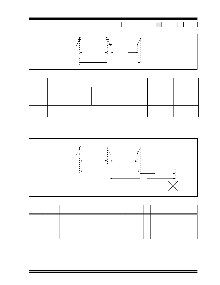
©
1996 Microchip Technology Inc.
DS30412C-page 187
PIC17C4X
Applicable Devices 42 R42 42A 43 R43 44
FIGURE 19-5: TIMER0 CLOCK TIMINGS
TABLE 19-5:
TIMER0 CLOCK REQUIREMENTS
FIGURE 19-6: TIMER1, TIMER2, AND TIMER3 CLOCK TIMINGS
TABLE 19-6:
TIMER1, TIMER2, AND TIMER3 CLOCK REQUIREMENTS
Parameter
No.
Sym Characteristic
Min
Typ Max Units Conditions
40
Tt0H T0CKI High Pulse Width
No Prescaler
0.5T
CY
+ 20 ß
--
--
ns
With Prescaler
10*
--
--
ns
41
Tt0L T0CKI Low Pulse Width
No Prescaler
0.5T
CY
+ 20 ß
--
--
ns
With Prescaler
10*
--
--
ns
42
Tt0P T0CKI Period
Greater of:
20 ns or Tcy + 40 ß
N
--
--
ns
N = prescale value
(1, 2, 4, ..., 256)
*
These parameters are characterized but not tested.
Data in "Typ" column is at 5V, 25∞C unless otherwise stated. These parameters are for design guidance only and are not
tested.
ß
This specification ensured by design.
Parameter
No.
Sym
Characteristic
Min
Typ
Max
Units Conditions
45
Tt123H
TCLK12 and TCLK3 high time
0.5T
CY
+ 20 ß
--
--
ns
46
Tt123L
TCLK12 and TCLK3 low time
0.5T
CY
+ 20 ß
--
--
ns
47
Tt123P
TCLK12 and TCLK3 input period
T
CY
+ 40 ß
N
--
--
ns
N = prescale value
(1, 2, 4, 8)
48
TckE2tmrI Delay from selected External Clock Edge to
Timer increment
2T
OSC
ß
6Tosc ß
*
These parameters are characterized but not tested.
Data in "Typ" column is at 5V, 25
∞
C unless otherwise stated. These parameters are for design guidance only and are not
tested.
ß
This specification ensured by design.
RA1/T0CKI
40
41
42
TCLK12
45
46
or
TCLK3
TMRx
48
48
47

PIC17C4X
DS30412C-page 188
©
1996 Microchip Technology Inc.
Applicable Devices 42 R42 42A 43 R43 44
FIGURE 19-7: CAPTURE TIMINGS
TABLE 19-7:
CAPTURE REQUIREMENTS
FIGURE 19-8: PWM TIMINGS
TABLE 19-8:
PWM REQUIREMENTS
Parameter
No.
Sym Characteristic
Min
Typ Max Units Conditions
50
TccL Capture1 and Capture2 input low time
10 *
--
--
ns
51
TccH Capture1 and Capture2 input high time
10 *
--
--
ns
52
TccP Capture1 and Capture2 input period
2T
CY
ß
N
--
--
ns
N = prescale value
(4 or 16)
*
These parameters are characterized but not tested.
Data in "Typ" column is at 5V, 25
∞
C unless otherwise stated. These parameters are for design guidance only and are not
tested.
ß
This specification ensured by design.
Parameter
No.
Sym Characteristic
Min
Typ Max Units Conditions
53
TccR PWM1 and PWM2 output rise time
--
10 * 35 *ß
ns
54
TccF PWM1 and PWM2 output fall time
--
10 * 35 *ß
ns
*
These parameters are characterized but not tested.
Data in "Typ" column is at 5V, 25
∞
C unless otherwise stated. These parameters are for design guidance only and are not
tested.
ß
This specification ensured by design.
CAP1
and CAP2
(Capture Mode)
50
51
52
PWM1
and PWM2
(PWM Mode)
53
54

©
1996 Microchip Technology Inc.
DS30412C-page 189
PIC17C4X
Applicable Devices 42 R42 42A 43 R43 44
FIGURE 19-9: USART MODULE: SYNCHRONOUS TRANSMISSION (MASTER/SLAVE) TIMING
TABLE 19-9:
SYNCHRONOUS TRANSMISSION REQUIREMENTS
FIGURE 19-10: USART MODULE: SYNCHRONOUS RECEIVE (MASTER/SLAVE) TIMING
TABLE 19-10: SYNCHRONOUS RECEIVE REQUIREMENTS
Param
No.
Sym
Characteristic
Min
Typ
Max
Units Conditions
120
TckH2dtV SYNC XMIT (MASTER &
SLAVE)
Clock high to data out valid
PIC17CR42/42A/43/R43/44
--
--
50
ns
PIC17LCR42/42A/43/R43/44
--
--
75
ns
121
TckRF
Clock out rise time and fall time
(Master Mode)
PIC17CR42/42A/43/R43/44
--
--
25
ns
PIC17LCR42/42A/43/R43/44
--
--
40
ns
122
TdtRF
Data out rise time and fall time
PIC17CR42/42A/43/R43/44
--
--
25
ns
PIC17LCR42/42A/43/R43/44
--
--
40
ns
Data in "Typ" column is at 5V, 25
∞
C unless otherwise stated. These parameters are for design guidance only and are not
tested.
Parameter
No.
Sym
Characteristic
Min
Typ
Max
Units Conditions
125
TdtV2ckL
SYNC RCV (MASTER & SLAVE)
Data hold before CK
(DT hold time)
15
--
--
ns
126
TckL2dtl
Data hold after CK
(DT hold time)
15
--
--
ns
Data in "Typ" column is at 5V, 25
∞
C unless otherwise stated. These parameters are for design guidance only and are not
tested.
121
121
120
122
RA5/TX/CK
RA4/RX/DT
pin
pin
125
126
RA5/TX/CK
RA4/RX/DT
pin
pin

PIC17C4X
DS30412C-page 190
©
1996 Microchip Technology Inc.
Applicable Devices 42 R42 42A 43 R43 44
FIGURE 19-11: MEMORY INTERFACE WRITE TIMING (NOT SUPPORTED IN PIC17LC4X DEVICES)
TABLE 19-11: MEMORY INTERFACE WRITE REQUIREMENTS (NOT SUPPORTED IN PIC17LC4X
DEVICES)
Parameter
No.
Sym
Characteristic
Min
Typ
Max
Units Conditions
150
TadV2alL
AD<15:0> (address) valid to ALE
(address setup time)
0.25Tcy - 10
--
--
ns
151
TalL2adI
ALE
to address out invalid
(address hold time)
0
--
--
ns
152
TadV2wrL
Data out valid to WR
(data setup time)
0.25Tcy - 40
--
--
ns
153
TwrH2adI
WR
to data out invalid
(data hold time)
--
0.25T
CY
ß
--
ns
154
TwrL
WR pulse width
--
0.25T
CY
ß
--
ns
*
These parameters are characterized but not tested.
Data in "Typ" column is at 5V, 25
∞
C unless otherwise stated. These parameters are for design guidance only and are not
tested.
ß
This specification ensured by design.
OSC1
ALE
OE
WR
AD<15:0>
Q1
Q2
Q3
Q4
Q1
Q2
150
151
152
153
154
addr out
data out
addr out

©
1996 Microchip Technology Inc.
DS30412C-page 191
PIC17C4X
Applicable Devices 42 R42 42A 43 R43 44
FIGURE 19-12: MEMORY INTERFACE READ TIMING (NOT SUPPORTED IN PIC17LC4X DEVICES)
TABLE 19-12: MEMORY INTERFACE READ REQUIREMENTS (NOT SUPPORTED IN PIC17LC4X
DEVICES)
Parameter
No.
Sym
Characteristic
Min
Typ
Max
Units Conditions
150
TadV2alL
AD15:AD0 (address) valid to ALE
(address setup time)
0.25Tcy - 10
--
--
ns
151
TalL2adI
ALE
to address out invalid
(address hold time)
5*
--
--
ns
160
TadZ2oeL
AD15:AD0 hi-impedance to OE
0*
--
--
ns
161
ToeH2adD
OE
to AD15:AD0 driven
0.25Tcy - 15
--
--
ns
162
TadV2oeH
Data in valid before OE
(data setup time)
35
--
--
ns
163
ToeH2adI
OE
to data in invalid (data hold time)
0
--
--
ns
164
TalH
ALE pulse width
--
0.25T
CY
ß
--
ns
165
ToeL
OE pulse width
0.5Tcy - 35 ß
--
--
ns
166
TalH2alH
ALE
to ALE
(cycle time)
--
T
CY
ß
--
ns
167
Tacc
Address access time
--
--
0.75T
CY
- 30
ns
168
Toe
Output enable access time
(OE low to Data Valid)
--
--
0.5T
CY
- 45
ns
*
These parameters are characterized but not tested.
Data in "Typ" column is at 5V, 25
∞
C unless otherwise stated. These parameters are for design guidance only and are not
tested.
ß
This specification ensured by design.
OSC1
ALE
OE
AD<15:0>
WR
Q1
Q2
Q3
Data in
Addr out
150
151
160
166
165
162
163
161
'1'
'1'
Q4
Q1
Q2
Addr out
164
168
167

PIC17C4X
DS30412C-page 192
©
1996 Microchip Technology Inc.
NOTES:
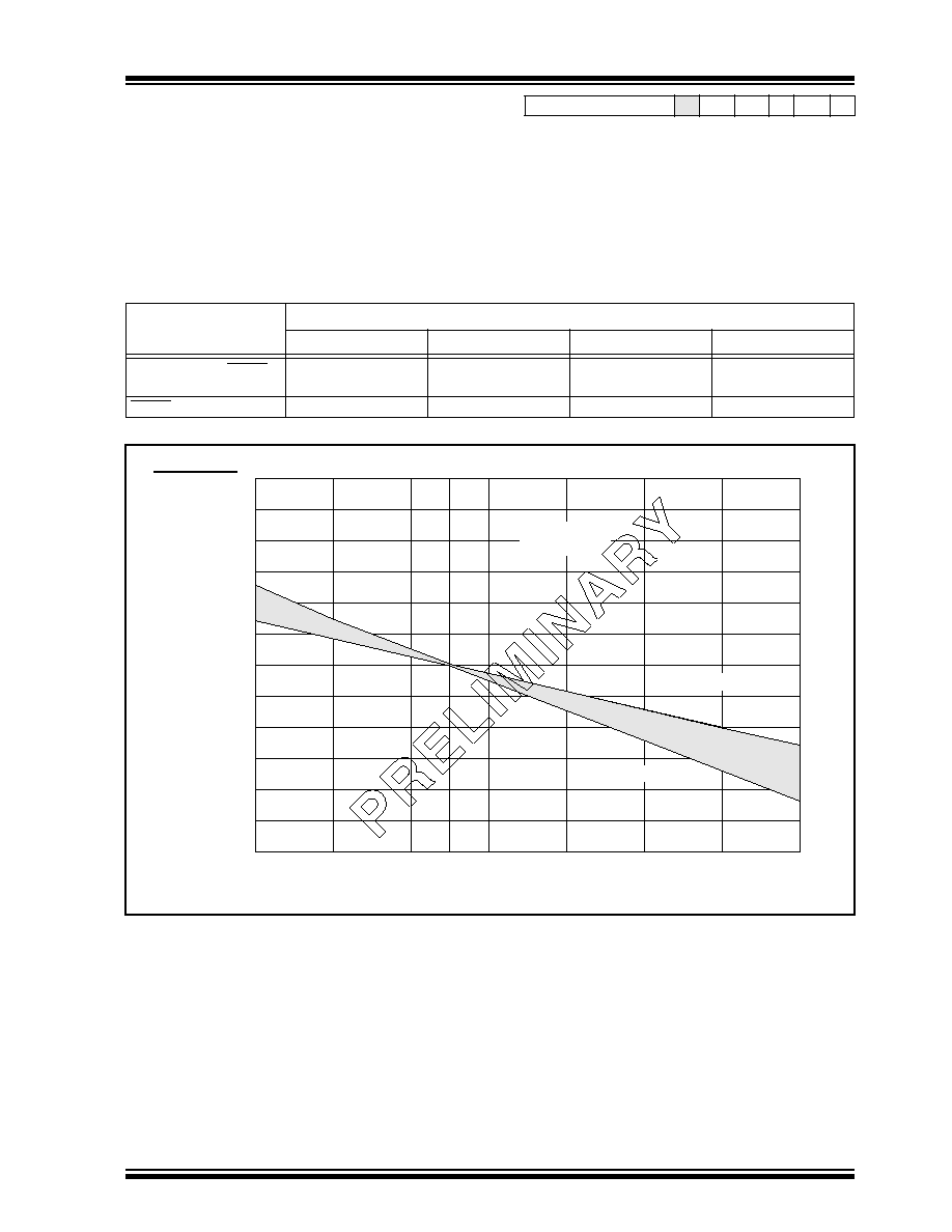
©
1996 Microchip Technology Inc.
DS30412C-page 193
PIC17C4X
Applicable Devices
42 R42 42A 43 R43 44
20.0
PIC17CR42/42A/43/R43/44 DC AND AC CHARACTERISTICS
The graphs and tables provided in this section are for design guidance and are not tested nor guaranteed. In some
graphs or tables the data presented is outside specified operating range (e.g. outside specified V
DD
range). This is for
information only and devices are ensured to operate properly only within the specified range.
The data presented in this section is a statistical summary of data collected on units from different lots over a period of
time. "Typical" represents the mean of the distribution while "max" or "min" represents (mean + 3
) and (mean - 3
)
respectively where
is standard deviation.
TABLE 20-1:
PIN CAPACITANCE PER PACKAGE TYPE
FIGURE 20-1: TYPICAL RC OSCILLATOR FREQUENCY vs. TEMPERATURE
Pin Name
Typical Capacitance (pF)
40-pin DIP
44-pin PLCC
44-pin MQFP
44-pin TQFP
All pins, except MCLR,
V
DD
, and V
SS
10
10
10
10
MCLR pin
20
20
20
20
F
OSC
F
OSC
(25
∞
C)
1.10
1.08
1.06
1.04
1.02
1.00
0.98
0.96
0.94
0.92
0.90
0
10
20
25
30
40
50
60
70
T(
∞
C)
Frequency normalized to +25
∞
C
V
DD
= 5.5V
V
DD
= 3.5V
Rext
10 k
Cext = 100 pF
This document was created with FrameMaker 4 0 4

PIC17C4X
DS30412C-page 194
©
1996 Microchip Technology Inc.
Applicable Devices
42 R42 42A 43 R43 44
FIGURE 20-2: TYPICAL RC OSCILLATOR FREQUENCY vs. V
DD
FIGURE 20-3: TYPICAL RC OSCILLATOR FREQUENCY vs. V
DD
4.0
3.5
3.0
2.5
2.0
1.5
1.0
0.5
0.0
4.0
4.5
5.0
5.5
6.0
6.5
F
OSC
(MHz)
V
DD
(Volts)
R = 10k
Cext = 22 pF, T = 25
∞
C
R = 100k
4.0
3.5
3.0
2.5
2.0
1.5
1.0
0.5
0.0
4.0
4.5
5.0
5.5
6.0
6.5
F
OSC
(MHz)
V
DD
(Volts)
R = 10k
Cext = 100 pF, T = 25
∞
C
R = 100k
R = 3.3k
R = 5.1k

©
1996 Microchip Technology Inc.
DS30412C-page 195
PIC17C4X
Applicable Devices
42 R42 42A 43 R43 44
FIGURE 20-4: TYPICAL RC OSCILLATOR FREQUENCY vs. V
DD
TABLE 20-2:
RC OSCILLATOR FREQUENCIES
Cext
Rext
Average
Fosc @ 5V, 25
∞
C
22 pF
10k
3.33 MHz
±
12%
100k
353 kHz
±
13%
100 pF
3.3k
3.54 MHz
±
10%
5.1k
2.43 MHz
±
14%
10k
1.30 MHz
±
17%
100k
129 kHz
±
10%
300 pF
3.3k
1.54 MHz
±
14%
5.1k
980 kHz
±
12%
10k
564 kHz
±
16%
160k
35 kHz
±
18%
2.0
1.8
1.6
1.4
1.2
1.0
0.8
0.6
0.4
4.0
4.5
5.0
5.5
6.0
6.5
F
OSC
(MHz)
V
DD
(Volts)
R = 10k
Cext = 300 pF, T = 25
∞
C
R = 160k
R = 3.3k
R = 5.1k
0.2
0.0

PIC17C4X
DS30412C-page 196
©
1996 Microchip Technology Inc.
Applicable Devices
42 R42 42A 43 R43 44
FIGURE 20-5: TRANSCONDUCTANCE (gm) OF LF OSCILLATOR vs. V
DD
FIGURE 20-6: TRANSCONDUCTANCE (gm) OF XT OSCILLATOR vs. V
DD
500
450
400
350
300
250
200
150
100
2.5
3.0
3.5
4.0
4.5
5.0
gm(
µ
A/V)
V
DD
(Volts)
Min @ 85
∞
C
50
0
5.5
6.0
Max @ -40
∞
C
Typ @ 25
∞
C
20
18
16
14
12
10
8
6
4
2.5
3.0
3.5
4.0
4.5
5.0
gm(mA/V)
V
DD
(Volts)
Min @ 85
∞
C
2
0
5.5
6.0
Max @ -40
∞
C
Typ @ 25
∞
C
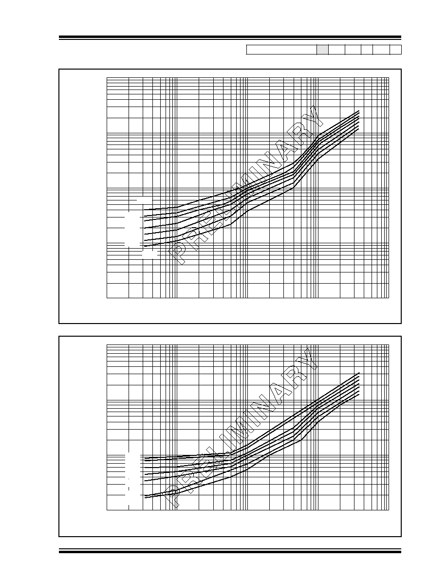
©
1996 Microchip Technology Inc.
DS30412C-page 197
PIC17C4X
Applicable Devices
42 R42 42A 43 R43 44
FIGURE 20-7: TYPICAL I
DD
vs. FREQUENCY (EXTERNAL CLOCK 25
∞
C)
FIGURE 20-8: MAXIMUM I
DD
vs. FREQUENCY (EXTERNAL CLOCK 125
∞
C TO -40
∞
C)
10k
100k
1M
10M
100M
100
1000
10000
100000
I
DD
(
µ
A)
External Clock Frequency (Hz)
7.0V
10
6.5V
6.0V
5.5V
4.5V
5.0V
4.0V
10k
100k
1M
10M
100M
100
1000
10000
100000
I
DD
(
µ
A)
External Clock Frequency (Hz)
6.5V
6.0V
5.5V
4.0V
4.5V
5.0V
7.0V
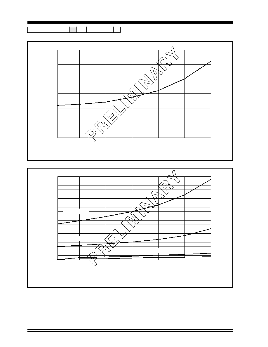
PIC17C4X
DS30412C-page 198
©
1996 Microchip Technology Inc.
Applicable Devices
42 R42 42A 43 R43 44
FIGURE 20-9: TYPICAL I
PD
vs. V
DD
WATCHDOG DISABLED 25
∞
C
FIGURE 20-10: MAXIMUM I
PD
vs. V
DD
WATCHDOG DISABLED
12
10
8
6
4
4.0
4.5
5.0
5.5
6.0
I
PD
(nA)
V
DD
(Volts)
2
0
6.5
7.0
600
500
400
300
200
4.0
4.5
5.0
5.5
6.0
I
PD
(nA)
V
DD
(Volts)
100
0
6.5
7.0
1300
1200
1100
1000
900
800
700
1900
1800
1700
1600
1500
1400
Temp. = 85
∞
C
Temp. = 70
∞
C
Temp. = 0
∞
C
Temp. = -40
∞
C

©
1996 Microchip Technology Inc.
DS30412C-page 199
PIC17C4X
Applicable Devices
42 R42 42A 43 R43 44
FIGURE 20-11: TYPICAL I
PD
vs. V
DD
WATCHDOG ENABLED 25
∞
C
FIGURE 20-12: MAXIMUM I
PD
vs. V
DD
WATCHDOG ENABLED
30
25
20
15
10
4.0
4.5
5.0
5.5
6.0
I
PD
(
µ
A)
V
DD
(Volts)
5
0
6.5
7.0
60
50
40
30
20
4.0
4.5
5.0
5.5
6.0
I
PD
(
µ
A)
V
DD
(Volts)
10
0
6.5
7.0
-40
∞
C
0
∞
C
70
∞
C
85
∞
C

PIC17C4X
DS30412C-page 200
©
1996 Microchip Technology Inc.
Applicable Devices 42 R42 42A 43 R43 44
FIGURE 20-13: WDT TIMER TIME-OUT PERIOD vs. V
DD
FIGURE 20-14: I
OH
vs. V
OH
, V
DD
= 3V
30
25
20
15
10
4.0
4.5
5.0
5.5
6.0
V
DD
(Volts)
5
0
6.5
7.0
WDT P
e
r
iod (ms)
Max. 70
∞
C
Typ. 25
∞
C
Min. 0
∞
C
Min. -40
∞
C
Max. 85
∞
C
0
-2
-4
-6
-8
-10
-12
-14
0.0
0.5
1.0
1.5
2.0
2.5
I
OH
(mA)
V
DD
(Volts)
Min @ 85
∞
C
-16
-18
3.0
Max @ -40
∞
C
Typ @ 25
∞
C

©
1996 Microchip Technology Inc.
DS30412C-page 201
PIC17C4X
Applicable Devices 42 R42 42A 43 R43 44
FIGURE 20-15: I
OH
vs. V
OH
, V
DD
= 5V
FIGURE 20-16: I
OL
vs. V
OL
, V
DD
= 3V
0
-5
-10
-15
-20
-25
0.0
0.5
1.0
1.5
2.0
2.5
I
OH
(mA)
V
DD
(Volts)
-30
-35
3.0
Max @ -40
∞
C
Typ @ 25
∞
C
3.5
4.0
4.5
5.0
Min @ 85
∞
C
30
25
20
15
10
0.0
0.5
1.0
1.5
2.0
V
DD
(Volts)
5
0
2.5
3.0
I
OL
(mA)
Min. +85
∞
C
Typ. 25
∞
C
Max. -40
∞
C
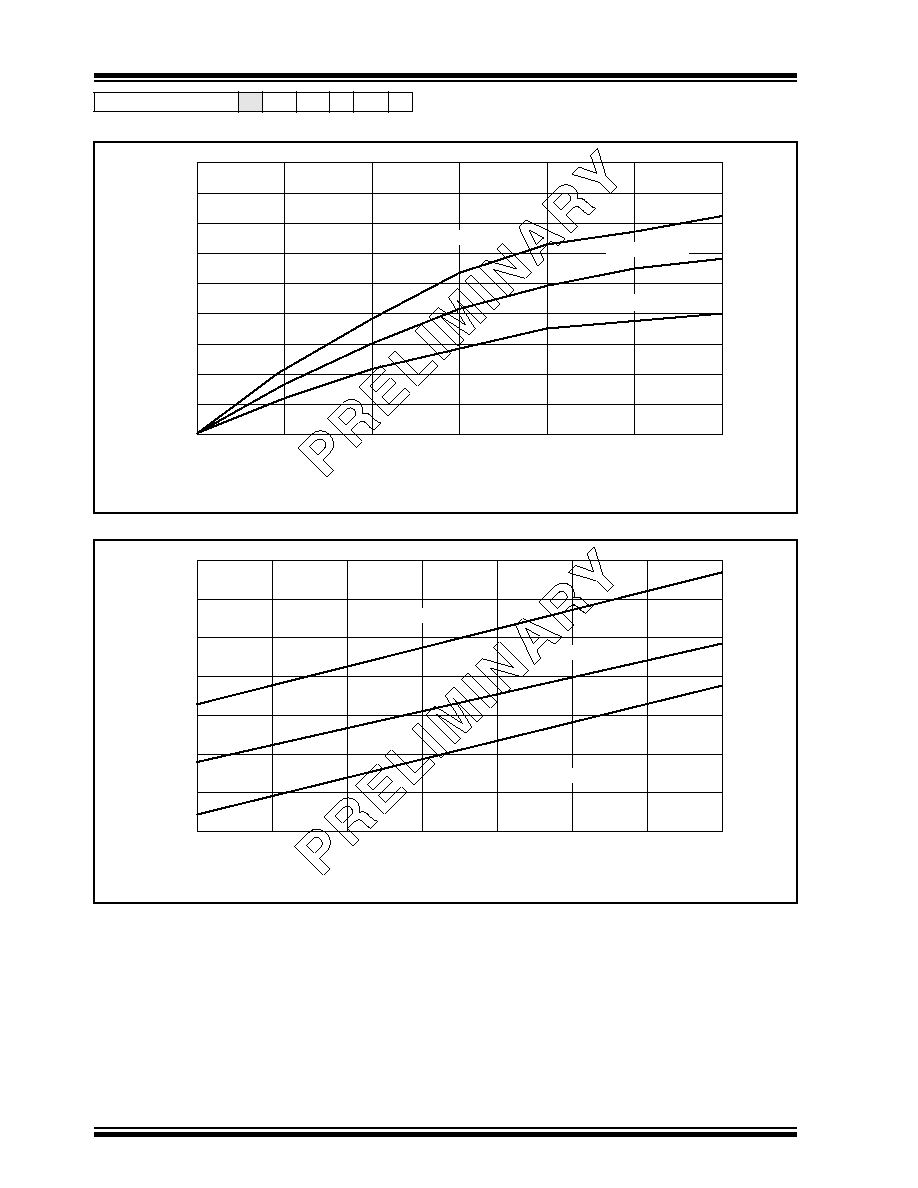
PIC17C4X
DS30412C-page 202
©
1996 Microchip Technology Inc.
Applicable Devices 42 R42 42A 43 R43 44
FIGURE 20-17: I
OL
vs. V
OL
, V
DD
= 5V
FIGURE 20-18: V
TH
(INPUT THRESHOLD VOLTAGE) OF I/O PINS (TTL)
VS
. V
DD
90
80
70
60
50
40
30
20
0.0
0.5
1.0
1.5
2.0
2.5
I
OH
(mA)
V
DD
(Volts)
Min @ +85
∞
C
10
0
3.0
Max @ -40
∞
C
Typ @ 25
∞
C
2.5
V
TH
(V
olts)
V
DD
(Volts)
0.6
Max (-40
∞
C to +85
∞
C)
Typ @ 25
∞
C
3.0
3.5
4.0
4.5
5.0
5.5
6.0
0.8
1.0
1.2
1.4
1.6
1.8
2.0
Min (-40
∞
C to +85
∞
C)
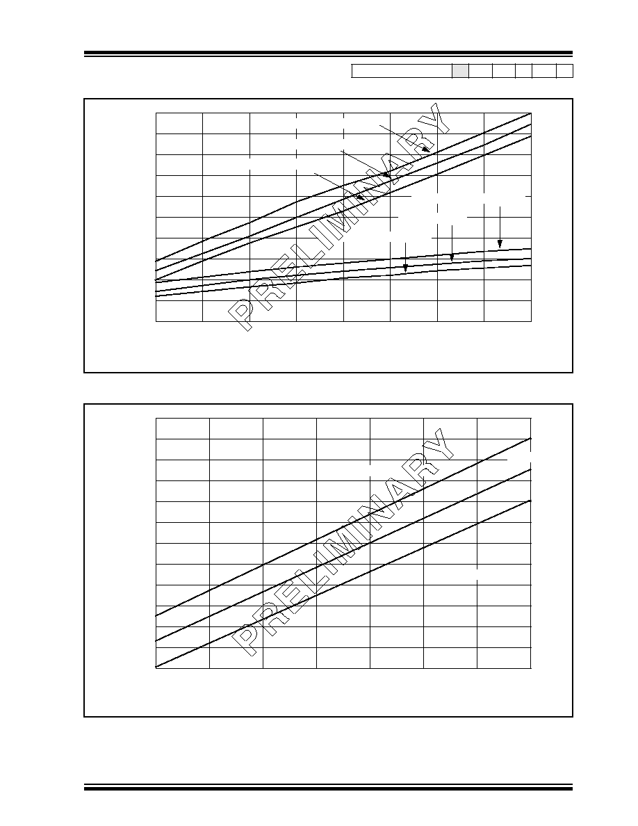
©
1996 Microchip Technology Inc.
DS30412C-page 203
PIC17C4X
Applicable Devices 42 R42 42A 43 R43 44
FIGURE 20-19: V
TH
, V
IL
of I/O PINS (SCHMITT TRIGGER)
VS
. V
DD
FIGURE 20-20: V
TH
(INPUT THRESHOLD VOLTAGE) OF OSC1 INPUT
(IN XT AND LF MODES) vs. V
DD
2.0
V
IH
, V
IL
(V
olts)
V
DD
(Volts)
0.0
2.5
3.0
3.5
4.0
4.5
5.0
5.5
0.5
1.0
1.5
2.0
2.5
3.0
3.5
6.0
4.0
4.5
5.0
V
IH
, max (-40
∞
C to +85
∞
C)
V
IH
, typ (25
∞
C)
V
IH
, min (-40
∞
C to +85
∞
C)
V
IL
, max (-40
∞
C to +85
∞
C)
V
IL
, typ (25
∞
C)
V
IL
, min (-40
∞
C to +85
∞
C)
V
TH
,(V
olts)
V
DD
(Volts)
1.0
2.5
3.0
3.5
4.0
4.5
5.0
5.5
1.2
1.4
1.6
1.8
2.0
2.2
2.4
6.0
2.6
2.8
3.0
Min (-40
∞
C to +85
∞
C)
3.2
3.4
Max (-40
∞
C to +85
∞
C)
Typ (25
∞
C)

PIC17C4X
DS30412C-page 204
©
1996 Microchip Technology Inc.
NOTES:

©
1996 Microchip Technology Inc.
DS30412C-page 205
PIC17C4X
21.0
PACKAGING INFORMATION
21.1
40-Lead Ceramic CERDIP Dual In-line, and CERDIP Dual In-line with Window (600 mil)
Package Group: Ceramic CERDIP Dual In-Line (CDP)
Symbol
Millimeters
Inches
Min
Max
Notes
Min
Max
Notes
0
∞
10
∞
0
∞
10
∞
A
4.318
5.715
0.170
0.225
A1
0.381
1.778
0.015
0.070
A2
3.810
4.699
0.150
0.185
A3
3.810
4.445
0.150
0.175
B
0.355
0.585
0.014
0.023
B1
1.270
1.651
Typical
0.050
0.065
Typical
C
0.203
0.381
Typical
0.008
0.015
Typical
D
51.435
52.705
2.025
2.075
D1
48.260
48.260
Reference
1.900
1.900
Reference
E
15.240
15.875
0.600
0.625
E1
12.954
15.240
0.510
0.600
e1
2.540
2.540
Reference
0.100
0.100
Reference
eA
14.986
16.002
Typical
0.590
0.630
Typical
eB
15.240
18.034
0.600
0.710
L
3.175
3.810
0.125
0.150
N
40
40
40
40
S
1.016
2.286
0.040
0.090
S1
0.381
1.778
0.015
0.070
N
Pin No. 1
Indicator
Area
E1
E
S
D
B1
B
D1
Base
Plane
Seating
Plane
S1
A1 A3 A A2
L
e1
C
e
A
e
B
This document was created with FrameMaker 4 0 4

PIC17C4X
DS30412C-page 206
©
1996 Microchip Technology Inc.
21.2
40-Lead Plastic Dual In-line (600 mil)
Package Group: Plastic Dual In-Line (PLA)
Symbol
Millimeters
Inches
Min
Max
Notes
Min
Max
Notes
0
∞
10
∞
0
∞
10
∞
A
≠
5.080
≠
0.200
A1
0.381
≠
0.015
≠
A2
3.175
4.064
0.125
0.160
B
0.355
0.559
0.014
0.022
B1
1.270
1.778
Typical
0.050
0.070
Typical
C
0.203
0.381
Typical
0.008
0.015
Typical
D
51.181
52.197
2.015
2.055
D1
48.260
48.260
Reference
1.900
1.900
Reference
E
15.240
15.875
0.600
0.625
E1
13.462
13.970
0.530
0.550
e1
2.489
2.591
Typical
0.098
0.102
Typical
eA
15.240
15.240
Reference
0.600
0.600
Reference
eB
15.240
17.272
0.600
0.680
L
2.921
3.683
0.115
0.145
N
40
40
40
40
S
1.270
≠
0.050
≠
S1
0.508
≠
0.020
≠
N
Pin No. 1
Indicator
Area
E1
E
S
D
B1
B
D1
Base
Plane
Seating
Plane
S1
A1 A2 A
L
e1
C
e
A
e
B

©
1996 Microchip Technology Inc.
DS30412C-page 207
PIC17C4X
21.3
44-Lead Plastic Leaded Chip Carrier (Square)
Package Group: Plastic Leaded Chip Carrier (PLCC)
Symbol
Millimeters
Inches
Min
Max
Notes
Min
Max
Notes
A
4.191
4.572
0.165
0.180
A1
2.413
2.921
0.095
0.115
D
17.399
17.653
0.685
0.695
D1
16.510
16.663
0.650
0.656
D2
15.494
16.002
0.610
0.630
D3
12.700
12.700
Reference
0.500
0.500
Reference
E
17.399
17.653
0.685
0.695
E1
16.510
16.663
0.650
0.656
E2
15.494
16.002
0.610
0.630
E3
12.700
12.700
Reference
0.500
0.500
Reference
N
44
44
44
44
CP
≠
0.102
≠
0.004
LT
0.203
0.381
0.008
0.015
S
0.177
.007
B D-E
-A-
0.254
D
1
D
3
3
3
-C-
-F-
-D-
4
9
8
-B-
-E-
S
0.177
.007
A F-G
S
S
E
E
1
-H-
-G-
6
2
3
.010 Max
1.524
.060
10
2
11
0.508
.020
1.651
.065
R 1.14/0.64
.045/.025
R 1.14/0.64
.045/.025
1.651
.065
0.508
.020
-H-
11
0.254
.010 Max
6
Min
0.812/0.661
.032/.026
3
-C-
0.64
.025
Min
5
0.533/0.331
.021/.013
0.177
.007 M A
F-G S , D-E S
1.27
.050
2 Sides
A
S
0.177
.007
B A
S
D
3
/E
3
D
2
0.101
.004
0.812/0.661
.032/.026
S
0.38
.015
F-G
4
S
0.38
.015
F-G
E
2
D
-H-
A
1
Seating
Plane
2 Sides
N Pics

PIC17C4X
DS30412C-page 208
©
1996 Microchip Technology Inc.
21.4
44-Lead Plastic Surface Mount (MQFP 10x10 mm Body 1.6/0.15 mm Lead Form)
Package Group: Plastic MQFP
Symbol
Millimeters
Inches
Min
Max
Notes
Min
Max
Notes
0
∞
7
∞
0
∞
7
∞
A
2.000
2.350
0.078
0.093
A1
0.050
0.250
0.002
0.010
A2
1.950
2.100
0.768
0.083
b
0.300
0.450
Typical
0.011
0.018
Typical
C
0.150
0.180
0.006
0.007
D
12.950
13.450
0.510
0.530
D1
9.900
10.100
0.390
0.398
D3
8.000
8.000
Reference
0.315
0.315
Reference
E
12.950
13.450
0.510
0.530
E1
9.900
10.100
0.390
0.398
E3
8.000
8.000
Reference
0.315
0.315
Reference
e
0.800
0.800
0.031
0.032
L
0.730
1.030
0.028
0.041
N
44
44
44
44
CP
0.102
≠
0.004
≠
Index
area
9
b
TYP 4x
Base
Plane
A
2
e
B
A
A
1
Seating
Plane
6
D
D
1
D
3
4
5
7
E
3
E
1
E
10
0.20 M
A-B
0.05 mm/mm D
H
S
S
D
0.20 M
A-B
C
S
S
D
7
5
4
0.20 M
A-B
C
S
S
D
0.20 M
A-B
H
S
S
D
0.05 mm/mm A-B
C
L
1.60 Ref.
0.13/0.30 R
0.13 R min.
0.20 min.
PARTING
LINE

©
1996 Microchip Technology Inc.
DS30412C-page 209
PIC17C4X
21.5
44-Lead Plastic Surface Mount (TQFP 10x10 mm Body 1.0/0.10 mm Lead Form)
Note 1: Dimensions D1 and E1 do not include mold protrusion. Allowable mold protrusion is 0.25m/m (0.010") per
side. D1 and E1 dimensions including mold mismatch.
2: Dimension "b" does not include Dambar protrusion, allowable Dambar protrusion shall be 0.08m/m
(0.003")max.
3: This outline conforms to JEDEC MS-026.
Package Group: Plastic TQFP
Symbol
Millimeters
Inches
Min
Max
Notes
Min
Max
Notes
A
1.00
1.20
0.039
0.047
A1
0.05
0.15
0.002
0.006
A2
0.95
1.05
0.037
0.041
D
11.75
12.25
0.463
0.482
D1
9.90
10.10
0.390
0.398
E
11.75
12.25
0.463
0.482
E1
9.90
10.10
0.390
0.398
L
0.45
0.75
0.018
0.030
e
0.80 BSC
0.031 BSC
b
0.30
0.45
0.012
0.018
b1
0.30
0.40
0.012
0.016
c
0.09
0.20
0.004
0.008
c1
0.09
0.16
0.004
0.006
N
44
44
44
44
0
∞
7
∞
0
∞
7
∞
D
E
D1
E1
Pin#1
2
e
1.0¯ (0.039¯) Ref.
Option 1 (TOP side)
Pin#1
2
Option 2 (TOP side)
3.0¯ (0.118¯) Ref.
Detail A
Detail B
L
1.00 Ref.
A2
A1
A
b
b1
c
c1
Base Metal
Detail A
Lead Finish
Detail B
11
∞
/13
∞
(4x)
0
∞
Min
11
∞
/13
∞
(4x)
R 1 0.08 Min
R 0.08/0.20
Gage Plane
0.250
L
L1
S
0.20
Min
1.00 Ref
Detail B

PIC17C4X
DS30412C-page 210
©
1996 Microchip Technology Inc.
21.6
Package Marking Information
44-Lead TQFP
XXXXXXXXXX
AABBCDE
XXXXXXXXXX
XXXXXXXXXX
44-Lead PLCC
XXXXXXXXXX
AABBCDE
XXXXXXXXXX
XXXXXXXXXX
XXXXXXXXXXXXXXXXXX
XXXXXXXXXXXXXXXXXX
AABBCDE
40-Lead PDIP/CERDIP
XXXXXXXXXXXXXXXXXX
XXXXXXXXXXX
XXXXXXXXXXX
AABBCDE
40 Lead CERDIP Windowed
XXXXXXXXXXX
Example
-25/TQ
9450CAT
PIC17C44
L247
Example
PIC17C42
9445CCN
-16I/L
L013
L006
9441CCA
Example
PIC17C43-25I/P
PIC17C44
9444CCT
Example
L184
/JW
Legend: MM...M
Microchip part number information
XX...X
Customer specific information*
AA
Year code (last 2 digits of calendar year)
BB
Week code (week of January 1 is week `01')
C
Facility code of the plant at which wafer is manufactured
C = Chandler, Arizona, U.S.A.,
S = Tempe, Arizona, U.S.A.
D
Mask revision number
E
Assembly code of the plant or country of origin in which
part was assembled
Note:
In the event the full Microchip part number cannot be marked on one line,
it will be carried over to the next line thus limiting the number of available
characters for customer specific information.
*
Standard OTP marking consists of Microchip part number, year code, week
code, facility code, mask rev#, and assembly code. For OTP marking beyond
this, certain price adders apply. Please check with your Microchip Sales
Office. For QTP devices, any special marking adders are included in QTP
price.
44-Lead MQFP
XXXXXXXXXX
AABBCDE
XXXXXXXXXX
XXXXXXXXXX
Example
-25/PT
9450CAT
PIC17C44
L247

©
1996 Microchip Technology Inc.
DS30412C-page 211
PIC17C4X
APPENDIX A: MODIFICATIONS
The following is the list of modifications over the
PIC16CXX microcontroller family:
1.
Instruction word length is increased to 16-bit.
This allows larger page sizes both in program
memory (8 Kwords verses 2 Kwords) and regis-
ter file (256 bytes versus 128 bytes).
2.
Four modes of operation: microcontroller, pro-
tected microcontroller, extended microcontroller,
and microprocessor.
3.
22 new instructions.
The
MOVF
,
TRIS
and
OPTION
instructions have
been removed.
4.
4 new instructions for transferring data between
data memory and program memory. This can be
used to "self program" the EPROM program
memory.
5.
Single cycle data memory to data memory trans-
fers possible (
MOVPF
and
MOVFP
instructions).
These instructions do not affect the Working reg-
ister (WREG).
6.
W register (WREG) is now directly addressable.
7.
A PC high latch register (PCLATH) is extended
to 8-bits. The PCLATCH register is now both
readable and writable.
8.
Data memory paging is redefined slightly.
9.
DDR registers replaces function of TRIS regis-
ters.
10. Multiple Interrupt vectors added. This can
decrease the latency for servicing the interrupt.
11. Stack size is increased to 16 deep.
12. BSR register for data memory paging.
13. Wake up from SLEEP operates slightly differ-
ently.
14. The Oscillator Start-Up Timer (OST) and
Power-Up Timer (PWRT) operate in parallel and
not in series.
15. PORTB interrupt on change feature works on all
eight port pins.
16. TMR0 is 16-bit plus 8-bit prescaler.
17. Second indirect addressing register added
(FSR1 and FSR2). Configuration bits can select
the FSR registers to auto-increment, auto-dec-
rement, remain unchanged after an indirect
address.
18. Hardware multiplier added (8 x 8
16-bit)
(PIC17C43 and PIC17C44 only).
19. Peripheral modules operate slightly differently.
20. Oscillator modes slightly redefined.
21. Control/Status bits and registers have been
placed in different registers and the control bit
for globally enabling interrupts has inverse
polarity.
22. Addition of a test mode pin.
23. In-circuit serial programming is not imple-
mented.
APPENDIX B: COMPATIBILITY
To convert code written for PIC16CXX to PIC17CXX,
the user should take the following steps:
1.
Remove any
TRIS
and
OPTION
instructions,
and implement the equivalent code.
2.
Separate the interrupt service routine into its
four vectors.
3.
Replace:
MOVF REG1, W
with:
MOVFP REG1, WREG
4.
Replace:
MOVF REG1, W
MOVWF REG2
with:
MOVPF REG1, REG2 ; Addr(REG1)<20h
or
MOVFP REG1, REG2 ; Addr(REG2)<20h
5.
Ensure that all bit names and register names are
updated to new data memory map location.
6.
Verify data memory banking.
7.
Verify mode of operation for indirect addressing.
8.
Verify peripheral routines for compatibility.
9.
Weak pull-ups are enabled on reset.
To convert code from the PIC17C42 to all the other
PIC17C4X devices, the user should take the following
steps.
1.
If the hardware multiply is to be used, ensure
that any variables at address 18h and 19h are
moved to another address.
2.
Ensure that the upper nibble of the BSR was not
written with a non-zero value. This may cause
unexpected operation since the RAM bank is no
longer 0.
3.
The disabling of global interrupts has been
enhanced so there is no additional testing of the
GLINTD bit after a
BSF CPUSTA, GLINTD
instruction.
Note:
If REG1 and REG2 are both at addresses
greater then 20h, two instructions are
required.
MOVFP REG1, WREG ;
MOVPF WREG, REG2 ;
This document was created with FrameMaker 4 0 4

PIC17C4X
DS30412C-page 212
©
1996 Microchip Technology Inc.
APPENDIX C: WHAT'S NEW
The structure of the document has been made consis-
tent with other data sheets. This ensures that important
topics are covered across all PIC16/17 families. Here is
an overview of new features.
Added the following devices:
PIC17CR42
PIC17C42A
PIC17CR43
A 33 MHz option is now available.
APPENDIX D: WHAT'S CHANGED
To make software more portable across the different
PIC16/17 families, the name of several registers and
control bits have been changed. This allows control bits
that have the same function, to have the same name
(regardless of processor family). Care must still be
taken, since they may not be at the same special func-
tion register address. The following shows the register
and bit names that have been changed:
Instruction DECFSNZ corrected to DCFSNZ
Instruction INCFSNZ corrected to INFSNZ
Enhanced discussion on PWM to include equation for
determining bits of PWM resolution.
Section 13.2.2 and 13.3.2 have had the description of
updating the FERR and RX9 bits enhanced.
The location of configuration bit PM2 was changed
(Figure 6-1 and Figure 14-1).
Enhanced description of the operation of the INTSTA
register.
Added note to discussion of interrupt operation.
Tightened electrical spec D110.
Corrected steps for setting up USART Asynchronous
Reception.
Old Name
New Name
TX8/9
TX9
RC8/9
RX9
RCD8
RX9D
TXD8
TX9D
PIC17C4X
©
1996 Microchip Technology Inc.
DS30412C-page 213
APPENDIX E: PIC16/17 MICROCONTROLLERS
E.1
PIC14000 Devices
PIC14000
20
4K
192
TMR0
ADTMR
I
2
C/
SMBus
14
11
22
2.7-6.0
Yes
Internal Oscillator,
Bandgap Reference,
Temperature Sensor,
Calibration Factors,
Low Voltage Detector,
SLEEP, HIBERNATE,
Comparators with
Programmable References
(2)
28-pin DIP, SOIC, SSOP
(.300 mil)
Maximum Frequency of Operation (MHz)
Data Memory (bytes)
Timer Module(s)
Serial Port(s) (SPI/I
2
C, USART)
Slope A/D Converter
Interrupt Sources
I/O Pins
Voltage Range (Volts)
EPROM Program Memory (x14 words)
Clock
Memory
Peripherals
Features
In-Circuit Serial Programming
Additional On-chip
Features
Packages
(high-res) Channels
This document was created with FrameMaker 4 0 4

PIC17C4X
DS30412C-page 214
©
1996 Microchip Technology Inc.
E.2
PIC16C5X Family of Devices
PIC16C52
4
384
--
2
5
TMR0
12
2.5-6.25
33
18-pin DIP, SOIC
PIC16C54
20
512
--
25
TMR0
12
2.5-6.25
33
18-pin DIP, SOIC; 20-pin SSOP
PIC16C54A
20
512
--
2
5
TMR0
12
2.0-6.25
33
18-pin DIP, SOIC; 20-pin SSOP
PIC16CR54A
20
--
512
25
TMR0
12
2.0-6.25
33
18-pin DIP, SOIC; 20-pin SSOP
PIC16C55
20
512
--
24
TMR0
20
2.5-6.25
33
28-pin DIP, SOIC, SSOP
PIC16C56
20
1K
--
25
TMR0
12
2.5-6.25
33
18-pin DIP, SOIC; 20-pin SSOP
PIC16C57
20
2K
--
72
TMR0
20
2.5-6.25
33
28-pin DIP, SOIC, SSOP
PIC16CR57B
20
--
2
K
7
2
TMR0
20
2.5-6.25
33
28-pin DIP, SOIC, SSOP
PIC16C58A
20
2K
--
73
TMR0
12
2.0-6.25
33
18-pin DIP, SOIC; 20-pin SSOP
PIC16CR58A
20
--
2K
73
TMR0
12
2.5-6.25
33
18-pin DIP, SOIC; 20-pin SSOP
All PIC16/17 F
amily de
vices ha
v
e
P
o
w
er-On Reset, selectab
le
W
atchdog
Timer
, selectab
le code protect and high I/O current capability
.
Packages
Number of Instructions
Voltage Range (Volts)
I/O Pins
Timer Module(s)
RAM Data Memory (bytes)
(x12 words)
Program Memory
ROM
EPROM
Maximum Frequency of Operation (MHz)
Features
Peripherals
Memory
Clock

PIC17C4X
©
1996 Microchip Technology Inc.
DS30412C-page 215
E.3
PIC16CXXX Family of Devices
PIC16C554
20
512
80
TMR0
--
--3
13
2.5-6.0
--
18-pin DIP
, SOIC;
20-pin SSOP
PIC16C556
20
1K
80
TMR0
--
--
3
13
2.5-6.0
--
18-pin DIP
, SOIC;
20-pin SSOP
PIC16C558
20
2K
128
TMR0
--
--
3
13
2.5-6.0
--
18-pin DIP
, SOIC;
20-pin SSOP
PIC16C620
20
512
80
TMR0
2
Ye
s
4
13
2.5-6.0
Ye
s
18-pin DIP
, SOIC;
20-pin SSOP
PIC16C621
20
1K
80
TMR0
2
Ye
s
4
13
2.5-6.0
Ye
s
18-pin DIP
, SOIC;
20-pin SSOP
PIC16C622
20
2K
128
TMR0
2
Ye
s
4
13
2.5-6.0
Ye
s
18-pin DIP
, SOIC;
20-pin SSOP
All PIC16/17 F
amily de
vices ha
v
e
P
o
w
er-on Reset, selectab
le
W
atchdog
Timer
, selectab
le code protect and high I/O
current capability
.
All PIC16C6XXX F
amily de
vices use ser
ial prog
r
amming with cloc
k pin RB6 and data pin RB7.
Maximum Frequency of Operation (MHz)
EPROM
Data Memory (bytes)
Timer Module(s)
Comparator(s)
Internal Reference Voltage
Interrupt Sources
I/O Pins
Voltage Range (Volts)
Brown-out
Reset
Packages
Program Memory
Clock
Memory
Peripherals
Features
(x14 words)

PIC17C4X
DS30412C-page 216
©
1996 Microchip Technology Inc.
E.4
PIC16C6X Family of Devices
PIC16C62
20
2K
--
128
TMR0,
TMR1, TMR2
1
SPI/I
2
C
--
7
22
3.0-6.0
Yes
--
28-pin SDIP, SOIC, SSOP
PIC16C62A
(1)
20
2K
--
128
TMR0,
TMR1, TMR2
1
SPI/I
2
C
--
7
22
2.5-6.0
Yes
Yes
28-pin SDIP, SOIC, SSOP
PIC16CR62
(1)
20
--
2K
128
TMR0,
TMR1, TMR2
1
SPI/I
2
C
--
7
22
2.5-6.0
Yes
Yes
28-pin SDIP, SOIC, SSOP
PIC16C63
20
4K
--
192
TMR0,
TMR1, TMR2
2
SPI/I
2
C,
USART
--
10
22
2.5-6.0
Yes
Yes
28-pin SDIP, SOIC
PIC16CR63
(1)
20
--
4K
192
TMR0,
TMR1, TMR2
2
SPI/I
2
C,
USART
--
10
22
2.5-6.0
Yes
Yes
28-pin SDIP, SOIC
PIC16C64
20
2K
--
128
TMR0,
TMR1, TMR2
1
SPI/I
2
C
Yes
8
3
3
3.0-6.0
Yes
--
40-pin DIP;
44-pin PLCC, MQFP
PIC16C64A
(1)
20
2K
--
128
TMR0,
TMR1, TMR2
1
SPI/I
2
C
Yes
8
3
3
2.5-6.0
Yes
Yes
40-pin DIP;
44-pin PLCC, MQFP, TQFP
PIC16CR64
(1)
20
--
2
K
128
TMR0,
TMR1, TMR2
1
SPI/I
2
C
Yes
8
3
3
2.5-6.0
Yes
Yes
40-pin DIP;
44-pin PLCC, MQFP, TQFP
PIC16C65
20
4K
--
192
TMR0,
TMR1, TMR2
2
SPI/I
2
C,
USART
Yes
11
33
3.0-6.0
Yes
--
40-pin DIP;
44-pin PLCC, MQFP
PIC16C65A
(1)
20
4K
--
192
TMR0,
TMR1, TMR2
2
SPI/I
2
C,
USART
Yes
11
33
2.5-6.0
Yes
Yes
40-pin DIP;
44-pin PLCC, MQFP, TQFP
PIC16CR65
(1)
20
--
4
K
192
TMR0,
TMR1, TMR2
2
SPI/I
2
C,
USART
Yes
11
33
2.5-6.0
Yes
Yes
40-pin DIP;
44-pin PLCC, MQFP, TQFP
All PIC16/17 f
amily de
vices ha
v
e
P
o
w
er-on Reset, selectab
le
W
atchdog
Timer
, selectab
le code protect, and high I/O current capability
.
All PIC16C6X f
amily de
vices use ser
ial prog
r
amming with cloc
k pin RB6 and data pin RB7.
Note
1:
Please contact y
our local sales office f
or a
v
ailability of these de
vices
.
Maximum Frequency of Operation (MHz)
EPROM
Data Memory (bytes)
Timer Module(s)
Capture/Compare/PWM Module(s)
Serial Port(s) (SPI/I
2
C, USART)
Parallel Slave Port
Interrupt Sources
I/O Pins
Voltage Range (Volts)
Brown-out Reset
Packages
Program Memory
Clock
Memory
Peripherals
Features
ROM
In-Circuit Serial Programming
(x14 words)

PIC17C4X
©
1996 Microchip Technology Inc.
DS30412C-page 217
E.5
PIC16C7X Family of Devices
PIC16C710
20
512
36
TMR0
--
--
--
4
4
13
3.0-6.0
Yes
Yes
18-pin DIP, SOIC;
20-pin SSOP
PIC16C71
20
1K
36
TMR0
--
--
--
4
4
1
3
3.0-6.0
Yes
--
18-pin DIP, SOIC
PIC16C711
20
1K
68
TMR0
--
--
--
4
4
13
3.0-6.0
Yes
Yes
18-pin DIP, SOIC;
20-pin SSOP
PIC16C72
20
2K
128
TMR0,
TMR1, TMR2
1
SPI/I
2
C
--
5
8
22
2.5-6.0
Yes
Yes
28-pin SDIP, SOIC, SSOP
PIC16C73
20
4K
192
TMR0,
TMR1, TMR2
2
SPI/I
2
C,
USART
--
5
11
22
3.0-6.0
Yes
--
28-pin SDIP, SOIC
PIC16C73A
(1)
20
4K
192
TMR0,
TMR1, TMR2
2
SPI/I
2
C,
USART
--
5
11
22
2.5-6.0
Yes
Yes
28-pin SDIP, SOIC
PIC16C74
20
4K
192
TMR0,
TMR1, TMR2
2
SPI/I
2
C,
USART
Yes
8
1
2
3
3
3.0-6.0
Yes
--
40-pin DIP;
44-pin PLCC, MQFP
PIC16C74A
(1)
20
4K
192
TMR0,
TMR1, TMR2
2
SPI/I
2
C,
USART
Yes
8
12
33
2.5-6.0
Yes
Yes
40-pin DIP;
44-pin PLCC, MQFP, TQFP
All PIC16/17 F
amily de
vices ha
v
e
P
o
w
er-on Reset, selectab
le
W
atchdog
Timer
, selectab
le code protect and high I/O current
capability
.
All PIC16C7X F
amily de
vices use ser
ial prog
r
amming with cloc
k pin RB6 and data pin RB7.
Note
1:
Please contact y
our local sales office f
or a
v
ailability of these de
vices
.
Maximum Frequency of Operation (MHz)
EPR
OM Prog
ram Memor
y (x14 w
ords)
Data Memory (bytes)
Timer Module(s)
Capture/Compare/PWM Module(s)
Serial Port(s) (SPI/I
2
C, USART)
Parallel Slave Port
A/D Converter (8-bit) Channels
Interrupt Sources
I/O Pins
Voltage Range (Volts)
Brown-out Reset
Packages
Clock
Memory
Peripherals
Features
In-Circuit Serial Programming

PIC17C4X
DS30412C-page 218
©
1996 Microchip Technology Inc.
E.6
PIC16C8X Family of Devices
PIC16C84
10
--
1
K
--
36
64
TMR0
4
1
3
2.0-6.0
18-pin DIP, SOIC
PIC16F84
(1)
10
1K
--
--
68
64
TMR0
4
1
3
2.0-6.0
18-pin DIP, SOIC
PIC16CR84
(1)
10
--
--
1K
68
64
TMR0
4
1
3
2.0-6.0
18-pin DIP, SOIC
PIC16F83
(1)
10
512
--
--
36
64
TMR0
4
1
3
2.0-6.0
18-pin DIP, SOIC
PIC16CR83
(1)
10
--
--
512
36
64
TMR0
4
1
3
2.0-6.0
18-pin DIP, SOIC
All PIC16/17 f
amily de
vices ha
v
e
P
o
w
er-on Reset, selectab
le
W
atchdog
Timer
, selectab
le code protect, and
high I/O current capability
.
All PIC16C8X f
amily de
vices use ser
ial prog
r
amming with cloc
k pin RB6 and data pin RB7.
Note
1:
Please contact y
our local sales office f
or a
v
ailability of these de
vices
.
Maximum Frequency of Operation (MHz)
EEPROM
Data EEPROM (bytes)
Data Memory (bytes)
Timer Module(s)
Interrupt Sources
I/O Pins
Voltage Range (Volts)
Packages
Program Memory
Clock
Memory
Peripherals
Features
ROM
Flash

PIC17C4X
©
1996 Microchip Technology Inc.
DS30412C-page 219
E.7
PIC16C9XX Family Of Devices
PIC16C923
8
4K
176
TMR0,
TMR1, TMR2
1
SPI/I
2
C
--
--
4 Com
32 Seg
8
25
27
3.0-6.0
Yes
--
64-pin SDIP
(1)
, TQFP,
68-pin PLCC, DIE
PIC16C924
8
4K
176
TMR0,
TMR1, TMR2
1
SPI/I
2
C
--
5
4 Com
32 Seg
9
25
27
3.0-6.0
Yes
--
64-pin SDIP
(1)
, TQFP,
68-pin PLCC, DIE
All PIC16/17 F
amily de
vices ha
v
e
P
o
w
er-on Reset, selectab
le
W
atchdog
Timer
, selectab
le code protect and high I/O current capability
.
All PIC16CXX F
amily de
vices use ser
ial prog
r
amming with cloc
k pin RB6 and data pin RB7.
Note
1:
Please contact y
our local Microchip representativ
e f
or a
v
ailability of this pac
kage
.
Maximum Frequency of Operation (MHz)
EPROM
Data Memory (bytes)
Timer Module(s)
Capture/Compare/PWM Module(s)
Serial Port(s) (SPI/I
2
C, USART)
Parallel Slave Port
A/D Converter (8-bit) Channels
Interrupt Sources
I/O Pins
Voltage Range (Volts)
Brown-out Reset
Packages
Program Memory
Clock
Memory
Peripherals
Features
In-Circuit Serial Programming
Input Pins
LCD Module
PIC17C4X
DS30412C-page 220
©
1996 Microchip Technology Inc.
E.8
PIC17CXX Family of Devices
PIC17C42
25
2K
--
232
TMR0,TMR1,
TMR2,TMR3
2
2
Yes
--
Yes
11
33
4.5-5.5
55
40-pin DIP;
44-pin PLCC, MQFP
PIC17C42A
25
2K
--
232
TMR0,TMR1,
TMR2,TMR3
2
2
Yes
Yes
Yes
11
33
2.5-6.0
58
40-pin DIP;
44-pin PLCC, TQFP, MQFP
PIC17CR42
25
--
2
K
232
TMR0,TMR1,
TMR2,TMR3
2
2
Yes
Yes
Yes
11
33
2.5-6.0
58
40-pin DIP;
44-pin PLCC, TQFP, MQFP
PIC17C43
25
4K
--
454
TMR0,TMR1,
TMR2,TMR3
2
2
Yes
Yes
Yes
11
33
2.5-6.0
58
40-pin DIP;
44-pin PLCC, TQFP, MQFP
PIC17CR43
25
--
4
K
454
TMR0,TMR1,
TMR2,TMR3
2
2
Yes
Yes
Yes
11
33
2.5-6.0
58
40-pin DIP;
44-pin PLCC, TQFP, MQFP
PIC17C44
25
8K
454
TMR0,TMR1,
TMR2,TMR3
2
2
Yes
Yes
Yes
11
33
2.5-6.0
58
40-pin DIP;
44-pin PLCC, TQFP, MQFP
All PIC16/17 F
amily de
vices ha
v
e
P
o
w
er-on Reset, selectab
le
W
atchdog
Timer
, selectab
le code protect and high I/O current capability
.
Maximum Frequency of Operation (MHz)
EPR
OM
RAM Data Memory (bytes)
Timer Module(s)
Captures
Serial Port(s) (USART)
External Interrupts
Interrupt Sources
I/O Pins
Voltage Range (Volts)
Number of Instructions
Packages
Clock
Memory
Peripherals
Features
PWMs
Hardware Multiply
Prog
ram Memor
y (W
ords)
RO
M

©
1996 Microchip Technology Inc.
DS30412C-page 221
PIC17C4X
PIN COMPATIBILITY
Devices that have the same package type and V
DD
,
V
SS
and MCLR pin locations are said to be pin
compatible. This allows these different devices to
operate in the same socket. Compatible devices may
only requires minor software modification to allow
proper operation in the application socket
(ex.,
PIC16C56 and PIC16C61 devices). Not all
devices in the same package size are pin compatible;
for example, the PIC16C62 is compatible with the
PIC16C63, but not the PIC16C55.
Pin compatibility does not mean that the devices offer
the same features. As an example, the PIC16C54 is
pin compatible with the PIC16C71, but does not have
an A/D converter, weak pull-ups on PORTB, or
interrupts.
TABLE E-1:
PIN COMPATIBLE DEVICES
Pin Compatible Devices
Package
PIC12C508, PIC12C509
8-pin
PIC16C54, PIC16C54A,
PIC16CR54A,
PIC16C56,
PIC16C58A, PIC16CR58A,
PIC16C61,
PIC16C554, PIC16C556, PIC16C558
PIC16C620, PIC16C621, PIC16C622,
PIC16C710, PIC16C71, PIC16C711,
PIC16F83, PIC16CR83,
PIC16C84, PIC16F84A, PIC16CR84
18-pin
20-pin
PIC16C55,
PIC16C57, PIC16CR57B
28-pin
PIC16C62, PIC16CR62, PIC16C62A, PIC16C63,
PIC16C72, PIC16C73, PIC16C73A
28-pin
PIC16C64, PIC16CR64, PIC16C64A,
PIC16C65, PIC16C65A,
PIC16C74, PIC16C74A
40-pin
PIC17C42, PIC17CR42, PIC17C42A,
PIC17C43, PIC17CR43, PIC17C44
40-pin
PIC16C923, PIC16C924
64/68-pin

PIC17C4X
DS30412C-page 222
©
1996 Microchip Technology Inc.
NOTES:

©
1996 Microchip Technology Inc.
DS30412C-page 223
PIC17C4X
APPENDIX F: ERRATA FOR
PIC17C42 SILICON
The PIC17C42 devices that you have received have the
following anomalies. At present there is no intention for
future revisions to the present PIC17C42 silicon. If
these cause issues for the application, it is recom-
mended that you select the PIC17C42A device.
1.
When the Oscillator Start-Up Timer (OST) is
enabled (in LF or XT oscillator modes), any inter-
rupt that wakes the processor may cause a WDT
reset. This occurs when the WDT is greater than
or equal to 50% time-out period when the
SLEEP
instruction is executed. This will not occur in
either the EC or RC oscillator modes.
Work-arounds
a)
Always ensure that the
CLRWDT
instruction is
executed before the WDT increments past 50%
of the WDT period. This will keep the "false"
WDT reset from occurring.
b)
When using the WDT as a normal timer (WDT
disabled), ensure that the WDT is less than or
equal to 50% time-out period when the
SLEEP
instruction is executed. This can be done by
monitoring the TO bit for changing state from set
to clear. Example 1 shows putting the PIC17C42
to sleep.
EXAMPLE F-1:
PIC17C42 TO SLEEP
BTFSS CPUSTA, TO ; TO = 0?
CLRWDT ; YES, WDT = 0
LOOP BTFSC CPUSTA, TO ; WDT rollover?
GOTO LOOP ; NO, Wait
SLEEP ; YES, goto Sleep
2.
When the clock source of Timer1 or Timer2 is
selected to external clock, the overflow interrupt
flag will be set twice, once when the timer equals
the period, and again when the timer value is
reset to 0h. If the latency to clear TMRxIF is
greater than the time to the next clock pulse, no
problems will be noticed. If the latency is less
than the time to the next timer clock pulse, the
interrupt will be serviced twice.
Work-arounds
a)
Ensure that the timer has rolled over to 0h before
clearing the flag bit.
b)
Clear the timer in software. Clearing the timer in
software causes the period to be one count less
than expected.
Note:
New designs should use the PIC17C42A.
Design considerations
The device must not be operated outside of the speci-
fied voltage range. An external reset circuit must be
used to ensure the device is in reset when a brown-out
occurs or the V
DD
rise time is too long. Failure to
ensure that the device is in reset when device voltage
is out of specification may cause the device to lock-up
and ignore the MCLR pin.
This document was created with FrameMaker 4 0 4

PIC17C4X
DS30412C-page 224
©
1996 Microchip Technology Inc.
NOTES:

©
1996 Microchip Technology Inc.
DS30412C-page 225
PIC17C4X
INDEX
A
ADDLW ............................................................................ 112
ADDWF ............................................................................ 112
ADDWFC ......................................................................... 113
ALU ...................................................................................... 9
ALU STATUS Register (ALUSTA) ..................................... 36
ALUSTA ............................................................... 34, 36, 108
ALUSTA Register ............................................................... 36
ANDLW ............................................................................ 113
ANDWF ............................................................................ 114
Application Notes
AN552 ........................................................................ 55
Assembler ........................................................................ 144
Asynchronous Master Transmission .................................. 90
Asynchronous Transmitter ................................................. 89
B
Bank Select Register (BSR) ............................................... 42
Banking .............................................................................. 42
Baud Rate Formula ............................................................ 86
Baud Rate Generator (BRG) .............................................. 86
Baud Rates
Asynchronous Mode .................................................. 88
Synchronous Mode .................................................... 87
BCF .................................................................................. 114
Bit Manipulation ............................................................... 108
Block Diagrams
On-chip Reset Circuit ................................................. 15
PIC17C42 .................................................................. 10
PORTD ...................................................................... 60
PORTE ....................................................................... 62
PWM .......................................................................... 75
RA0 and RA1 ............................................................. 53
RA2 and RA3 ............................................................. 54
RA4 and RA5 ............................................................. 54
RB3:RB2 Port Pins .................................................... 56
RB7:RB4 and RB1:RB0 Port Pins ............................. 55
RC7:RC0 Port Pins .................................................... 58
Timer3 with One Capture and One Period Register .. 78
TMR1 and TMR2 in 16-bit Timer/Counter Mode ........ 74
TMR1 and TMR2 in Two 8-bit Timer/Counter Mode .. 73
TMR3 with Two Capture Registers ............................ 79
WDT ......................................................................... 104
BORROW ............................................................................ 9
BRG ................................................................................... 86
Brown-out Protection ......................................................... 18
BSF .................................................................................. 115
BSR .............................................................................. 34, 42
BSR Operation ................................................................... 42
BTFSC ............................................................................. 115
BTFSS ............................................................................. 116
BTG .................................................................................. 116
C
C .................................................................................... 9, 36
C Compiler (MP-C) .......................................................... 145
CA1/PR3 ............................................................................ 72
CA1ED0 ............................................................................. 71
CA1ED1 ............................................................................. 71
CA1IE .................................................................................23
CA1IF .................................................................................24
CA1OVF .............................................................................72
CA2ED0 ..............................................................................71
CA2ED1 ..............................................................................71
CA2H ............................................................................20, 35
CA2IE ...........................................................................23, 78
CA2IF ...........................................................................24, 78
CA2L .............................................................................20, 35
CA2OVF .............................................................................72
Calculating Baud Rate Error ...............................................86
CALL ...........................................................................39, 117
Capacitor Selection
Ceramic Resonators .................................................101
Crystal Oscillator ......................................................101
Capture .........................................................................71, 78
Capture Sequence to Read Example .................................78
Capture1
Mode ...........................................................................71
Overflow .....................................................................72
Capture2
Mode ...........................................................................71
Overflow .....................................................................72
Carry (C) ...............................................................................9
Ceramic Resonators .........................................................100
Circular Buffer .....................................................................39
Clearing the Prescaler ......................................................103
Clock/Instruction Cycle (Figure) .........................................14
Clocking Scheme/Instruction Cycle (Section) .....................14
CLRF ................................................................................117
CLRWDT ..........................................................................118
Code Protection ..........................................................99, 106
COMF ...............................................................................118
Configuration
Bits ............................................................................100
Locations ..................................................................100
Oscillator ...................................................................100
Word ...........................................................................99
CPFSEQ ...........................................................................119
CPFSGT ...........................................................................119
CPFSLT ............................................................................120
CPU STATUS Register (CPUSTA) ....................................37
CPUSTA ...............................................................34, 37, 105
CREN .................................................................................84
Crystal Operation, Overtone Crystals ...............................101
Crystal or Ceramic Resonator Operation .........................100
Crystal Oscillator ..............................................................100
CSRC .................................................................................83
D
Data Memory
GPR ......................................................................29, 32
Indirect Addressing .....................................................39
Organization ...............................................................32
SFR ......................................................................29, 32
Transfer to Program Memory .....................................43
DAW .................................................................................120
DC ..................................................................................9, 36
DDRB .....................................................................19, 34, 55
DDRC .....................................................................19, 34, 58
DDRD .....................................................................19, 34, 60
DDRE .....................................................................19, 34, 62
DECF ................................................................................121
DECFSNZ .........................................................................122
DECFSZ ...........................................................................121
This document was created with FrameMaker 4 0 4

PIC17C4X
DS30412C-page 226
©
1996 Microchip Technology Inc.
Delay From External Clock Edge ....................................... 68
Development Support ...................................................... 143
Development Tools .......................................................... 143
Device Drawings
44-Lead Plastic Surface Mount (MQFP
10x10 mm Body 1.6/0.15 mm Lead Form) .............. 209
DIGIT BORROW .................................................................. 9
Digit Carry (DC) .................................................................... 9
Duty Cycle .......................................................................... 75
E
Electrical Characteristics
PIC17C42
Absolute Maximum Ratings ............................. 147
Capture Timing ................................................ 159
CLKOUT and I/O Timing .................................. 156
DC Characteristics ........................................... 149
External Clock Timing ...................................... 155
Memory Interface Read Timing ........................ 162
Memory Interface Write Timing ........................ 161
PWM Timing .................................................... 159
RESET, Watchdog Timer, Oscillator Start-up
Timer and Power-up Timer .............................. 157
Timer0 Clock Timings ...................................... 158
Timer1, Timer2 and Timer3 Clock Timing ........ 158
USART Module, Synchronous Receive ........... 160
USART Module, Synchronous Transmission ... 160
PIC17C43/44
Absolute Maximum Ratings ............................. 175
Capture Timing ................................................ 188
CLKOUT and I/O Timing .................................. 185
DC Characteristics ........................................... 177
External Clock Timing ...................................... 184
Memory Interface Read Timing ........................ 191
Memory Interface Write Timing ........................ 190
Parameter Measurement Information .............. 183
RESET, Watchdog Timer, Oscillator Start-up
Timer and Power-up Timer Timing .................. 186
Timer0 Clock Timing ........................................ 187
Timer1, Timer2 and Timer3 Clock Timing ........ 187
Timing Parameter Symbology .......................... 182
USART Module Synchronous Receive
Timing .............................................................. 189
USART Module Synchronous Transmission
Timing .............................................................. 189
EPROM Memory Access Time Order Suffix ...................... 31
Extended Microcontroller ................................................... 29
Extended Microcontroller Mode ......................................... 31
External Memory Interface ................................................. 31
External Program Memory Waveforms .............................. 31
F
Family of Devices ................................................................. 6
PIC14000 .................................................................. 213
PIC16C5X ................................................................ 214
PIC16CXXX .............................................................. 215
PIC16C6X ................................................................ 216
PIC16C7X ................................................................ 217
PIC16C8X ................................................................ 218
PIC16C9XX............................................................... 219
PIC17CXX ................................................................ 220
FERR ........................................................................... 84, 91
FOSC0 ............................................................................... 99
FOSC1 ............................................................................... 99
FS0 .................................................................................... 36
FS1 .................................................................................... 36
FS2 .................................................................................... 36
FS3 .................................................................................... 36
FSR0 ............................................................................ 34, 40
FSR1 ............................................................................ 34, 40
Fuzzy Logic Dev. System (
fuzzy
TECH
Æ
-MP) .......... 143, 145
G
General Format for Instructions ....................................... 108
General Purpose RAM ....................................................... 29
General Purpose RAM Bank ............................................. 42
General Purpose Register (GPR) ...................................... 32
GLINTD .......................................................... 25, 37, 78, 105
GOTO .............................................................................. 122
GPR (General Purpose Register) ...................................... 32
Graphs
I
OH
vs. V
OH
, V
DD
= 3V ..................................... 170, 200
I
OH
vs. V
OH
, V
DD
= 5V ..................................... 171, 201
I
OL
vs. V
OL
, V
DD
= 3V ...................................... 171, 201
I
OL
vs. V
OL
, V
DD
= 5V ...................................... 172, 202
Maximum I
DD
vs. Frequency
(External Clock 125
∞
C to -40
∞
C) ...................... 167, 197
Maximum I
PD
vs. V
DD
Watchdog Disabled ...... 168, 198
Maximum I
PD
vs. V
DD
Watchdog Enabled ...... 169, 199
RC Oscillator Frequency vs.
V
DD
(Cext = 100 pF) ........................................ 164, 194
RC Oscillator Frequency vs.
V
DD
(Cext = 22 pF) .......................................... 164, 194
RC Oscillator Frequency vs.
V
DD
(Cext = 300 pF) ........................................ 165, 195
Transconductance of LF Oscillator vs.V
DD
...... 166, 196
Transconductance of XT Oscillator vs. V
DD
.... 166, 196
Typical I
DD
vs. Frequency
(External Clock 25
∞
C) ...................................... 167, 197
Typical I
PD
vs. V
DD
Watchdog Disabled 25
∞
C . 168, 198
Typical I
PD
vs. V
DD
Watchdog Enabled 25
∞
C .. 169, 199
Typical RC Oscillator vs. Temperature ............ 163, 193
V
TH
(Input Threshold Voltage) of I/O Pins vs.
V
DD
.................................................................. 172, 202
V
TH
(Input Threshold Voltage) of OSC1 Input
(In XT, HS, and LP Modes) vs. V
DD
................ 173, 203
V
TH
, V
IL
of MCLR, T0CKI and OSC1
(In RC Mode) vs. V
DD
...................................... 173, 203
WDT Timer Time-Out Period vs. V
DD
.............. 170, 200
H
Hardware Multiplier ............................................................ 49
I
I/O Ports
Bi-directional .............................................................. 64
I/O Ports .................................................................... 53
Programming Considerations .................................... 64
Read-Modify-Write Instructions ................................. 64
Successive Operations .............................................. 64
INCF ................................................................................ 123
INCFSNZ ......................................................................... 124
INCFSZ ............................................................................ 123
INDF0 .......................................................................... 34, 40
INDF1 .......................................................................... 34, 40

©
1996 Microchip Technology Inc.
DS30412C-page 227
PIC17C4X
Indirect Addressing
Indirect Addressing .................................................... 39
Operation ................................................................... 40
Registers .................................................................... 40
Initialization Conditions For Special Function Registers .... 19
Initializing PORTB .............................................................. 57
Initializing PORTC .............................................................. 58
Initializing PORTD .............................................................. 60
Initializing PORTE .............................................................. 62
Instruction Flow/Pipelining ................................................. 14
Instruction Set .................................................................. 110
ADDLW .................................................................... 112
ADDWF .................................................................... 112
ADDWFC ................................................................. 113
ANDLW .................................................................... 113
ANDWF .................................................................... 114
BCF .......................................................................... 114
BSF .......................................................................... 115
BTFSC ..................................................................... 115
BTFSS ..................................................................... 116
BTG .......................................................................... 116
CALL ........................................................................ 117
CLRF ........................................................................ 117
CLRWDT .................................................................. 118
COMF ...................................................................... 118
CPFSEQ .................................................................. 119
CPFSGT .................................................................. 119
CPFSLT ................................................................... 120
DAW ......................................................................... 120
DECF ....................................................................... 121
DECFSNZ ................................................................ 122
DECFSZ ................................................................... 121
GOTO ...................................................................... 122
INCF ......................................................................... 123
INCFSNZ ................................................................. 124
INCFSZ .................................................................... 123
IORLW ..................................................................... 124
IORWF ..................................................................... 125
LCALL ...................................................................... 125
MOVFP .................................................................... 126
MOVLB .................................................................... 126
MOVLR .................................................................... 127
MOVLW ................................................................... 127
MOVPF .................................................................... 128
MOVWF ................................................................... 128
MULLW .................................................................... 129
MULWF .................................................................... 129
NEGW ...................................................................... 130
NOP ......................................................................... 130
RETFIE .................................................................... 131
RETLW .................................................................... 131
RETURN .................................................................. 132
RLCF ........................................................................ 132
RLNCF ..................................................................... 133
RRCF ....................................................................... 133
RRNCF .................................................................... 134
SETF ........................................................................ 134
SLEEP ..................................................................... 135
SUBLW .................................................................... 135
SUBWF .................................................................... 136
SUBWFB .................................................................. 136
SWAPF .................................................................... 137
TABLRD ........................................................... 137, 138
TABLWT .......................................................... 138, 139
TLRD ........................................................................ 139
TLWT ....................................................................... 140
TSTFSZ ....................................................................140
XORLW ....................................................................141
XORWF ....................................................................141
Instruction Set Summary ..................................................107
INT Pin ................................................................................26
INTE ...................................................................................22
INTEDG ........................................................................38, 67
Interrupt on Change Feature ..............................................55
Interrupt Status Register (INTSTA) ....................................22
Interrupts
Context Saving ...........................................................27
Flag bits
TMR1IE ..............................................................21
TMR1IF ..............................................................21
TMR2IE ..............................................................21
TMR2IF ..............................................................21
TMR3IE ..............................................................21
TMR3IF ..............................................................21
Interrupts ....................................................................21
Logic ...........................................................................21
Operation ....................................................................25
Peripheral Interrupt Enable .........................................23
Peripheral Interrupt Request ......................................24
PWM ...........................................................................76
Status Register ...........................................................22
Table Write Interaction ...............................................45
Timing .........................................................................26
Vectors
Peripheral Interrupt .............................................26
RA0/INT Interrupt ...............................................26
T0CKI Interrupt ...................................................26
TMR0 Interrupt ...................................................26
Vectors/Priorities ........................................................25
Wake-up from SLEEP ..............................................105
INTF ....................................................................................22
INTSTA ...............................................................................34
INTSTA Register ................................................................22
IORLW ..............................................................................124
IORWF ..............................................................................125
L
LCALL ...............................................................................125
Long Writes ........................................................................45
M
Memory
External Interface .......................................................31
External Memory Waveforms .....................................31
Memory Map (Different Modes) ..................................30
Mode Memory Access ................................................30
Organization ...............................................................29
Program Memory ........................................................29
Program Memory Map ................................................29
Microcontroller ....................................................................29
Microprocessor ...................................................................29
Minimizing Current Consumption .....................................106
MOVFP .............................................................................126
MOVLB .............................................................................126
MOVLR .............................................................................127
MOVLW ............................................................................127
MOVPF .............................................................................128
MOVWF ............................................................................128
MPASM Assembler ..................................................143, 144

PIC17C4X
DS30412C-page 228
©
1996 Microchip Technology Inc.
MP-C C Compiler ............................................................. 145
MPSIM Software Simulator ...................................... 143, 145
MULLW ............................................................................ 129
Multiply Examples
16 x 16 Routine .......................................................... 50
16 x 16 Signed Routine .............................................. 51
8 x 8 Routine .............................................................. 49
8 x 8 Signed Routine .................................................. 49
MULWF ............................................................................ 129
N
NEGW .............................................................................. 130
NOP ................................................................................. 130
O
OERR ................................................................................. 84
Opcode Field Descriptions ............................................... 107
OSC Selection .................................................................... 99
Oscillator
Configuration ............................................................ 100
Crystal ...................................................................... 100
External Clock .......................................................... 101
External Crystal Circuit ............................................ 102
External Parallel Resonant Crystal Circuit ............... 102
External Series Resonant Crystal Circuit ................. 102
RC ............................................................................ 102
RC Frequencies ............................................... 165, 195
Oscillator Start-up Time (Figure) ........................................ 18
Oscillator Start-up Timer (OST) ................................... 15, 99
OST .............................................................................. 15, 99
OV .................................................................................. 9, 36
Overflow (OV) ...................................................................... 9
P
Package Marking Information .......................................... 210
Packaging Information ..................................................... 205
Parameter Measurement Information .............................. 154
PC (Program Counter) ....................................................... 41
PCH .................................................................................... 41
PCL ...................................................................... 34, 41, 108
PCLATH ....................................................................... 34, 41
PD .............................................................................. 37, 105
PEIE ............................................................................. 22, 78
PEIF ................................................................................... 22
Peripheral Bank .................................................................. 42
Peripheral Interrupt Enable ................................................ 23
Peripheral Interrupt Request (PIR) ..................................... 24
PICDEM-1 Low-Cost PIC16/17 Demo Board ........... 143, 144
PICDEM-2 Low-Cost PIC16CXX Demo Board ........ 143, 144
PICDEM-3 Low-Cost PIC16C9XXX Demo Board ............ 144
PICMASTER
Æ
RT In-Circuit Emulator ............................. 143
PICSTART
Æ
Low-Cost Development System .................. 143
PIE ............................................................. 19, 34, 92, 96, 98
Pin Compatible Devices ................................................... 221
PIR ............................................................. 19, 34, 92, 96, 98
PM0 ............................................................................ 99, 106
PM1 ............................................................................ 99, 106
POP .............................................................................. 27, 39
POR ............................................................................. 15, 99
PORTA ................................................................... 19, 34, 53
PORTB ................................................................... 19, 34, 55
PORTC ................................................................... 19, 34, 58
PORTD .................................................................. 19, 34, 60
PORTE .................................................................. 19, 34, 62
Power-down Mode ........................................................... 105
Power-on Reset (POR) ................................................ 15, 99
Power-up Timer (PWRT) ............................................. 15, 99
PR1 .............................................................................. 20, 35
PR2 .............................................................................. 20, 35
PR3/CA1H ......................................................................... 20
PR3/CA1L .......................................................................... 20
PR3H/CA1H ....................................................................... 35
PR3L/CA1L ........................................................................ 35
Prescaler Assignments ...................................................... 69
PRO MATE
Æ
Universal Programmer ............................... 143
PRODH .............................................................................. 20
PRODL .............................................................................. 20
Program Counter (PC) ....................................................... 41
Program Memory
External Access Waveforms ...................................... 31
External Connection Diagram .................................... 31
Map ............................................................................ 29
Modes
Extended Microcontroller ................................... 29
Microcontroller ................................................... 29
Microprocessor .................................................. 29
Protected Microcontroller ................................... 29
Operation ................................................................... 29
Organization .............................................................. 29
Transfers from Data Memory ..................................... 43
Protected Microcontroller ................................................... 29
PS0 .............................................................................. 38, 67
PS1 .............................................................................. 38, 67
PS2 .............................................................................. 38, 67
PS3 .............................................................................. 38, 67
PUSH ........................................................................... 27, 39
PW1DCH ..................................................................... 20, 35
PW1DCL ...................................................................... 20, 35
PW2DCH ..................................................................... 20, 35
PW2DCL ...................................................................... 20, 35
PWM ............................................................................ 71, 75
Duty Cycle ................................................................. 76
External Clock Source ............................................... 76
Frequency vs. Resolution .......................................... 76
Interrupts ................................................................... 76
Max Resolution/Frequency for External
Clock Input ................................................................. 77
Output ........................................................................ 75
Periods ...................................................................... 76
PWM1 ................................................................................ 72
PWM1ON ..................................................................... 72, 75
PWM2 ................................................................................ 72
PWM2ON ..................................................................... 72, 75
PWRT .......................................................................... 15, 99
R
RA1/T0CKI pin ................................................................... 67
RBIE .................................................................................. 23
RBIF ................................................................................... 24
RBPU ................................................................................. 55
RC Oscillator .................................................................... 102
RC Oscillator Frequencies ....................................... 165, 195
RCIE .................................................................................. 23
RCIF .................................................................................. 24
RCREG ................................................ 19, 34, 91, 92, 96, 97
RCSTA ....................................................... 19, 34, 92, 96, 98
Reading 16-bit Value ......................................................... 69

©
1996 Microchip Technology Inc.
DS30412C-page 229
PIC17C4X
Receive Status and Control Register ................................. 83
Register File Map ............................................................... 33
Registers
ALUSTA ............................................................... 27, 36
BRG ........................................................................... 86
BSR ............................................................................ 27
CPUSTA .................................................................... 37
File Map ..................................................................... 33
FSR0 .......................................................................... 40
FSR1 .......................................................................... 40
INDF0 ......................................................................... 40
INDF1 ......................................................................... 40
INTSTA ...................................................................... 22
PIE ............................................................................. 23
PIR ............................................................................. 24
RCSTA ....................................................................... 84
Special Function Table .............................................. 34
T0STA .................................................................. 38, 67
TCON1 ....................................................................... 71
TCON2 ....................................................................... 72
TMR1 ......................................................................... 81
TMR2 ......................................................................... 81
TMR3 ......................................................................... 81
TXSTA ....................................................................... 83
WREG ........................................................................ 27
Reset
Section ....................................................................... 15
Status Bits and Their Significance ............................. 16
Time-Out in Various Situations .................................. 16
Time-Out Sequence ................................................... 16
RETFIE ............................................................................ 131
RETLW ............................................................................ 131
RETURN .......................................................................... 132
RLCF ................................................................................ 132
RLNCF ............................................................................. 133
RRCF ............................................................................... 133
RRNCF ............................................................................ 134
RX Pin Sampling Scheme .................................................. 91
RX9 .................................................................................... 84
RX9D ................................................................................. 84
S
Sampling ............................................................................ 91
Saving STATUS and WREG in RAM ................................. 27
SETF ................................................................................ 134
SFR .................................................................................. 108
SFR (Special Function Registers) ................................ 29, 32
SFR As Source/Destination ............................................. 108
Signed Math ......................................................................... 9
SLEEP ............................................................... 99, 105, 135
Software Simulator (MPSIM) ........................................... 145
SPBRG ...................................................... 19, 34, 92, 96, 98
Special Features of the CPU ............................................. 99
Special Function Registers ............................ 29, 32, 34, 108
SPEN ................................................................................. 84
SREN ................................................................................. 84
Stack
Operation ................................................................... 39
Pointer ........................................................................ 39
Stack .......................................................................... 29
STKAL ................................................................................ 39
STKAV ............................................................................... 37
SUBLW ............................................................................ 135
SUBWF ............................................................................ 136
SUBWFB .......................................................................... 136
SWAPF .............................................................................137
SYNC ..................................................................................83
Synchronous Master Mode .................................................93
Synchronous Master Reception .........................................95
Synchronous Master Transmission ....................................93
Synchronous Slave Mode ...................................................97
T
T0CKI Pin ...........................................................................26
T0CKIE ...............................................................................22
T0CKIF ...............................................................................22
T0CS ............................................................................38, 67
T0IE ....................................................................................22
T0IF ....................................................................................22
T0SE .............................................................................38, 67
T0STA ..........................................................................34, 38
T16 .....................................................................................71
Table Latch .........................................................................40
Table Pointer ......................................................................40
Table Read
Example ......................................................................48
Section ........................................................................43
Table Reads Section ..................................................48
TABLRD Operation .....................................................44
Timing .........................................................................48
TLRD ..........................................................................48
TLRD Operation .........................................................44
Table Write
Code ...........................................................................46
Interaction ...................................................................45
Section ........................................................................43
TABLWT Operation ....................................................43
Terminating Long Writes ............................................45
Timing .........................................................................46
TLWT Operation .........................................................43
To External Memory ...................................................46
To Internal Memory ....................................................45
TABLRD .............................................................44, 137, 138
TABLWT .............................................................43, 138, 139
TBLATH ..............................................................................40
TBLATL ..............................................................................40
TBLPTRH .....................................................................34, 40
TBLPTRL ......................................................................34, 40
TCLK12 ..............................................................................71
TCLK3 ................................................................................71
TCON1 .........................................................................20, 35
TCON2 .........................................................................20, 35
Terminating Long Writes ....................................................45
Time-Out Sequence ...........................................................16
Timer Resources ................................................................65
Timer0 ................................................................................67
Timer1
16-bit Mode .................................................................74
Clock Source Select ...................................................71
On bit ..........................................................................72
Section ..................................................................71, 73
Timer2
16-bit Mode .................................................................74
Clock Source Select ...................................................71
On bit ..........................................................................72
Section ..................................................................71, 73
Timer3
Clock Source Select ...................................................71
On bit ..........................................................................72
Section ..................................................................71, 77

PIC17C4X
DS30412C-page 230
©
1996 Microchip Technology Inc.
Timing Diagrams
Asynchronous Master Transmission .......................... 90
Asynchronous Reception ........................................... 92
Back to Back Asynchronous Master Transmission .... 90
Interrupt (INT, TMR0 Pins) ......................................... 26
PIC17C42 Capture ................................................... 159
PIC17C42 CLKOUT and I/O .................................... 156
PIC17C42 Memory Interface Read .......................... 162
PIC17C42 Memory Interface Write .......................... 161
PIC17C42 PWM Timing ........................................... 159
PIC17C42 RESET, Watchdog Timer, Oscillator
Start-up Timer and Power-up Timer ........................ 157
PIC17C42 Timer0 Clock .......................................... 158
PIC17C42 Timer1, Timer2 and Timer3 Clock .......... 158
PIC17C42 USART Module, Synchronous
Receive .................................................................... 160
PIC17C42 USART Module, Synchronous
Transmission ............................................................ 160
PIC17C43/44 Capture Timing .................................. 188
PIC17C43/44 CLKOUT and I/O ............................... 185
PIC17C43/44 External Clock ................................... 184
PIC17C43/44 Memory Interface Read ..................... 191
PIC17C43/44 Memory Interface Write ..................... 190
PIC17C43/44 PWM Timing ...................................... 188
PIC17C43/44 RESET, Watchdog Timer, Oscillator
Start-up Timer and Power-up Timer ........................ 186
PIC17C43/44 Timer0 Clock ..................................... 187
PIC17C43/44 Timer1, Timer2 and Timer3 Clock ..... 187
PIC17C43/44 USART Module Synchronous
Receive .................................................................... 189
PIC17C43/44 USART Module Synchronous
Transmission ............................................................ 189
Synchronous Reception ............................................. 95
Synchronous Transmission ........................................ 94
Table Read ................................................................ 48
Table Write ................................................................. 46
TMR0 ................................................................... 68, 69
TMR0 Read/Write in Timer Mode .............................. 70
TMR1, TMR2, and TMR3 in External Clock Mode ..... 80
TMR1, TMR2, and TMR3 in Timer Mode ................... 81
Wake-Up from SLEEP ............................................. 105
Timing Diagrams and Specifications ................................ 155
Timing Parameter Symbology .......................................... 153
TLRD .......................................................................... 44, 139
TLWT ......................................................................... 43, 140
TMR0
16-bit Read ................................................................ 69
16-bit Write ................................................................. 69
Clock Timing ............................................................ 158
Module ....................................................................... 68
Operation ................................................................... 68
Overview .................................................................... 65
Prescaler Assignments .............................................. 69
Read/Write Considerations ........................................ 69
Read/Write in Timer Mode ......................................... 70
Timing .................................................................. 68, 69
TMR0 STATUS/Control Register (T0STA) ......................... 38
TMR0H ............................................................................... 34
TMR0L ............................................................................... 34
TMR1 ........................................................................... 20, 35
8-bit Mode .................................................................. 73
External Clock Input ................................................... 73
Overview .................................................................... 65
Timer Mode ................................................................ 81
Timing in External Clock Mode .................................. 80
Two 8-bit Timer/Counter Mode .................................. 73
Using with PWM ........................................................ 75
TMR1CS ............................................................................ 71
TMR1IE .............................................................................. 23
TMR1IF .............................................................................. 24
TMR1ON ............................................................................ 72
TMR2 ........................................................................... 20, 35
8-bit Mode .................................................................. 73
External Clock Input .................................................. 73
In Timer Mode ........................................................... 81
Timing in External Clock Mode .................................. 80
Two 8-bit Timer/Counter Mode .................................. 73
Using with PWM ........................................................ 75
TMR2CS ............................................................................ 71
TMR2IE .............................................................................. 23
TMR2IF .............................................................................. 24
TMR2ON ............................................................................ 72
TMR3
Dual Capture1 Register Mode ................................... 79
Example, Reading From ............................................ 80
Example, Writing To .................................................. 80
External Clock Input .................................................. 80
In Timer Mode ........................................................... 81
One Capture and One Period Register Mode ........... 78
Overview .................................................................... 65
Reading/Writing ......................................................... 80
Timing in External Clock Mode .................................. 80
TMR3CS ...................................................................... 71, 77
TMR3H ........................................................................ 20, 35
TMR3IE .............................................................................. 23
TMR3IF ........................................................................ 24, 77
TMR3L ......................................................................... 20, 35
TMR3ON ...................................................................... 72, 77
TO ...................................................................... 37, 103, 105
Transmit Status and Control Register ................................ 83
TRMT ................................................................................. 83
TSTFSZ ........................................................................... 140
Turning on 16-bit Timer ..................................................... 74
TX9 .................................................................................... 83
TX9d .................................................................................. 83
TXEN ................................................................................. 83
TXIE ................................................................................... 23
TXIF ................................................................................... 24
TXREG ................................................ 19, 34, 89, 93, 97, 98
TXSTA ....................................................... 19, 34, 92, 96, 98
U
Upward Compatibility ........................................................... 5
USART
Asynchronous Master Transmission ......................... 90
Asynchronous Mode .................................................. 89
Asynchronous Receive .............................................. 91
Asynchronous Transmitter ......................................... 89
Baud Rate Generator ................................................ 86
Synchronous Master Mode ........................................ 93
Synchronous Master Reception ................................ 95
Synchronous Master Transmission ........................... 93
Synchronous Slave Mode .......................................... 97
Synchronous Slave Transmit ..................................... 97
W
Wake-up from SLEEP ...................................................... 105
Wake-up from SLEEP Through Interrupt ......................... 105
Watchdog Timer ........................................................ 99, 103

©
1996 Microchip Technology Inc.
DS30412C-page 231
PIC17C4X
WDT ........................................................................... 99, 103
Clearing the WDT .................................................... 103
Normal Timer ........................................................... 103
Period ....................................................................... 103
Programming Considerations .................................. 103
WDTPS0 ............................................................................ 99
WDTPS1 ............................................................................ 99
WREG ................................................................................ 34
X
XORLW ............................................................................ 141
XORWF ............................................................................ 141
Z
Z ..................................................................................... 9, 36
Zero (Z) ................................................................................ 9
LIST OF EXAMPLES
Example 3-1: Signed Math ..................................................9
Example 3-2: Instruction Pipeline Flow .............................14
Example 5-1: Saving STATUS and WREG in RAM ..........27
Example 6-1: Indirect Addressing......................................40
Example 7-1: Table Write ..................................................46
Example 7-2: Table Read..................................................48
Example 8-1: 8 x 8 Multiply Routine ..................................49
Example 8-2: 8 x 8 Signed Multiply Routine......................49
Example 8-3: 16 x 16 Multiply Routine ..............................50
Example 8-4: 16 x 16 Signed Multiply Routine..................51
Example 9-1: Initializing PORTB .......................................57
Example 9-2: Initializing PORTC .......................................58
Example 9-3: Initializing PORTD .......................................60
Example 9-4: Initializing PORTE .......................................62
Example 9-5: Read Modify Write Instructions on an
I/O Port ........................................................64
Example 11-1: 16-Bit Read .................................................69
Example 11-2: 16-Bit Write..................................................69
Example 12-1: Sequence to Read Capture Registers.........78
Example 12-2: Writing to TMR3 ..........................................80
Example 12-3: Reading from TMR3 ....................................80
Example 13-1: Calculating Baud Rate Error........................86
Example F-1: PIC17C42 to Sleep....................................223
LIST OF FIGURES
Figure 3-1:
PIC17C42 Block Diagram ...........................10
Figure 3-2:
PIC17CR42/42A/43/R43/44 Block
Diagram.......................................................11
Figure 3-3:
Clock/Instruction Cycle................................14
Figure 4-1:
Simplified Block Diagram of On-chip
Reset Circuit................................................15
Figure 4-2:
Time-Out Sequence on Power-Up
(MCLR Tied to V
DD
) ....................................17
Figure 4-3:
Time-Out Sequence on Power-Up
(MCLR
NOT
Tied to V
DD
)............................17
Figure 4-4:
Slow Rise Time (MCLR Tied to V
DD
) ..........17
Figure 4-5:
Oscillator Start-Up Time ..............................18
Figure 4-6:
Using On-Chip POR ....................................18
Figure 4-7:
Brown-out Protection Circuit 1.....................18
Figure 4-8:
PIC17C42 External Power-On Reset
Circuit (For Slow V
DD
Power-Up) ................18
Figure 4-9:
Brown-out Protection Circuit 2.....................18
Figure 5-1:
Interrupt Logic .............................................21
Figure 5-2:
INTSTA Register (Address: 07h,
Unbanked)...................................................22
Figure 5-3:
PIE Register (Address: 17h, Bank 1) ..........23
Figure 5-4:
PIR Register (Address: 16h, Bank 1) ..........24
Figure 5-5:
INT Pin / T0CKI Pin Interrupt Timing...........26
Figure 6-1:
Program Memory Map and Stack................29
Figure 6-2:
Memory Map in Different Modes .................30
Figure 6-3:
External Program Memory Access
Waveforms ..................................................31
Figure 6-4:
Typical External Program Memory
Connection Diagram....................................31
Figure 6-5:
PIC17C42 Register File Map.......................33
Figure 6-6:
PIC17CR42/42A/43/R43/44 Register
File Map.......................................................33
Figure 6-7:
ALUSTA Register (Address: 04h,
Unbanked)...................................................36
Figure 6-8:
CPUSTA Register (Address: 06h,
Unbanked)...................................................37
Figure 6-9:
T0STA Register (Address: 05h,
Unbanked)...................................................38
Figure 6-10:
Indirect Addressing......................................39
Figure 6-11:
Program Counter Operation ........................41

PIC17C4X
DS30412C-page 232
©
1996 Microchip Technology Inc.
Figure 6-12:
Program Counter using The CALL and
GOTO Instructions ...................................... 41
Figure 6-13:
BSR Operation (PIC17C43/R43/44) ........... 42
Figure 7-1:
TLWT Instruction Operation........................ 43
Figure 7-2:
TABLWT Instruction Operation ................... 43
Figure 7-3:
TLRD Instruction Operation ........................ 44
Figure 7-4:
TABLRD Instruction Operation ................... 44
Figure 7-5:
TABLWT Write Timing
(External Memory) ...................................... 46
Figure 7-6:
Consecutive TABLWT Write Timing
(External Memory) ...................................... 47
Figure 7-7:
TABLRD Timing .......................................... 48
Figure 7-8:
TABLRD Timing (Consecutive TABLRD
Instructions) ................................................ 48
Figure 9-1:
RA0 and RA1 Block Diagram ..................... 53
Figure 9-2:
RA2 and RA3 Block Diagram ..................... 54
Figure 9-3:
RA4 and RA5 Block Diagram ..................... 54
Figure 9-4:
Block Diagram of RB<7:4> and RB<1:0>
Port Pins ..................................................... 55
Figure 9-5:
Block Diagram of RB3 and RB2 Port Pins .. 56
Figure 9-6:
Block Diagram of RC<7:0> Port Pins ......... 58
Figure 9-7:
PORTD Block Diagram
(in I/O Port Mode) ....................................... 60
Figure 9-8:
PORTE Block Diagram
(in I/O Port Mode) ....................................... 62
Figure 9-9:
Successive I/O Operation ........................... 64
Figure 11-1:
T0STA Register (Address: 05h,
Unbanked) .................................................. 67
Figure 11-2:
Timer0 Module Block Diagram ................... 68
Figure 11-3:
TMR0 Timing with External Clock
(Increment on Falling Edge) ....................... 68
Figure 11-4:
TMR0 Timing: Write High or Low Byte ....... 69
Figure 11-5:
TMR0 Read/Write in Timer Mode ............... 70
Figure 12-1:
TCON1 Register (Address: 16h, Bank 3) ... 71
Figure 12-2:
TCON2 Register (Address: 17h, Bank 3) ... 72
Figure 12-3:
Timer1 and Timer2 in Two 8-bit
Timer/Counter Mode ................................... 73
Figure 12-4:
TMR1 and TMR2 in 16-bit Timer/Counter
Mode ........................................................... 74
Figure 12-5:
Simplified PWM Block Diagram .................. 75
Figure 12-6:
PWM Output ............................................... 75
Figure 12-7:
Timer3 with One Capture and One
Period Register Block Diagram................... 78
Figure 12-8:
Timer3 with Two Capture Registers
Block Diagram ............................................ 79
Figure 12-9:
TMR1, TMR2, and TMR3 Operation in
External Clock Mode................................... 80
Figure 12-10: TMR1, TMR2, and TMR3 Operation in
Timer Mode................................................. 81
Figure 13-1:
TXSTA Register (Address: 15h, Bank 0) .... 83
Figure 13-2:
RCSTA Register (Address: 13h, Bank 0) ... 84
Figure 13-3:
USART Transmit......................................... 85
Figure 13-4:
USART Receive.......................................... 85
Figure 13-5:
Asynchronous Master Transmission........... 90
Figure 13-6:
Asynchronous Master Transmission
(Back to Back) ............................................ 90
Figure 13-7:
RX Pin Sampling Scheme .......................... 91
Figure 13-8:
Asynchronous Reception ............................ 92
Figure 13-9:
Synchronous Transmission ........................ 94
Figure 13-10: Synchronous Transmission
(Through TXEN) ......................................... 94
Figure 13-11: Synchronous Reception (Master Mode,
SREN)......................................................... 95
Figure 14-1:
Configuration Word ..................................... 99
Figure 14-2:
Crystal or Ceramic Resonator Operation
(XT or LF OSC Configuration) .................. 100
Figure 14-3:
Crystal Operation, Overtone Crystals
(XT OSC Configuration) ........................... 101
Figure 14-4:
External Clock Input Operation
(EC OSC Configuration) ........................... 101
Figure 14-5:
External Parallel Resonant Crystal
Oscillator Circuit ....................................... 102
Figure 14-6:
External Series Resonant Crystal
Oscillator Circuit ....................................... 102
Figure 14-7:
RC Oscillator Mode .................................. 102
Figure 14-8:
Watchdog Timer Block Diagram............... 104
Figure 14-9:
Wake-up From Sleep Through Interrupt... 105
Figure 15-1:
General Format for Instructions................ 108
Figure 15-2:
Q Cycle Activity ........................................ 109
Figure 17-1:
Parameter Measurement Information....... 154
Figure 17-2:
External Clock Timing .............................. 155
Figure 17-3:
CLKOUT and I/O Timing .......................... 156
Figure 17-4:
Reset, Watchdog Timer,
Oscillator Start-Up Timer and
Power-Up Timer Timing ........................... 157
Figure 17-5:
Timer0 Clock Timings............................... 158
Figure 17-6:
Timer1, Timer2, And Timer3 Clock
Timings ..................................................... 158
Figure 17-7:
Capture Timings ....................................... 159
Figure 17-8:
PWM Timings ........................................... 159
Figure 17-9:
USART Module: Synchronous
Transmission (Master/Slave) Timing ........ 160
Figure 17-10: USART Module: Synchronous Receive
(Master/Slave) Timing .............................. 160
Figure 17-11: Memory Interface Write Timing ................ 161
Figure 17-12: Memory Interface Read Timing ................ 162
Figure 18-1:
Typical RC Oscillator Frequency
vs. Temperature ....................................... 163
Figure 18-2:
Typical RC Oscillator Frequency
vs. V
DD
..................................................... 164
Figure 18-3:
Typical RC Oscillator Frequency
vs. V
DD
..................................................... 164
Figure 18-4:
Typical RC Oscillator Frequency
vs. V
DD
..................................................... 165
Figure 18-5:
Transconductance (gm) of LF Oscillator
vs. V
DD
..................................................... 166
Figure 18-6:
Transconductance (gm) of XT Oscillator
vs. V
DD
..................................................... 166
Figure 18-7:
Typical I
DD
vs. Frequency (External
Clock 25
∞
C) .............................................. 167
Figure 18-8:
Maximum I
DD
vs. Frequency (External
Clock 125
∞
C to -40
∞
C) .............................. 167
Figure 18-9:
Typical I
PD
vs. V
DD
Watchdog
Disabled 25
∞
C .......................................... 168
Figure 18-10: Maximum I
PD
vs. V
DD
Watchdog
Disabled ................................................... 168
Figure 18-11: Typical I
PD
vs. V
DD
Watchdog
Enabled 25
∞
C ........................................... 169
Figure 18-12: Maximum I
PD
vs. V
DD
Watchdog
Enabled .................................................... 169
Figure 18-13: WDT Timer Time-Out Period vs. V
DD
...... 170
Figure 18-14: I
OH
vs. V
OH
, V
DD
= 3V.............................. 170
Figure 18-15: I
OH
vs. V
OH
, V
DD
= 5V.............................. 171
Figure 18-16: I
OL
vs. V
OL
, V
DD
= 3V............................... 171
Figure 18-17: I
OL
vs. V
OL
, V
DD
= 5V............................... 172
Figure 18-18: V
TH
(Input Threshold Voltage) of
I/O Pins (TTL)
VS
. V
DD
............................. 172
Figure 18-19: V
TH
, V
IL
of I/O Pins (Schmitt Trigger)
VS
.
V
DD
........................................................... 173
Figure 18-20: V
TH
(Input Threshold Voltage) of OSC1
Input (In XT and LF Modes) vs. V
DD
........ 173
Figure 19-1:
Parameter Measurement Information....... 183

©
1996 Microchip Technology Inc.
DS30412C-page 233
PIC17C4X
Figure 19-2:
External Clock Timing............................... 184
Figure 19-3:
CLKOUT and I/O Timing........................... 185
Figure 19-4:
Reset, Watchdog Timer,
Oscillator Start-Up Timer, and
Power-Up Timer Timing............................ 186
Figure 19-5:
Timer0 Clock Timings ............................... 187
Figure 19-6:
Timer1, Timer2, and Timer3 Clock
Timings ..................................................... 187
Figure 19-7:
Capture Timings ....................................... 188
Figure 19-8:
PWM Timings ........................................... 188
Figure 19-9:
USART Module: Synchronous
Transmission (Master/Slave) Timing ........ 189
Figure 19-10: USART Module: Synchronous
Receive (Master/Slave) Timing................. 189
Figure 19-11: Memory Interface Write Timing
(Not Supported in PIC17LC4X Devices)... 190
Figure 19-12: Memory Interface Read Timing
(Not Supported in PIC17LC4X Devices)... 191
Figure 20-1:
Typical RC Oscillator Frequency vs.
Temperature ............................................. 193
Figure 20-2:
Typical RC Oscillator Frequency
vs. V
DD
...................................................... 194
Figure 20-3:
Typical RC Oscillator Frequency
vs. V
DD
...................................................... 194
Figure 20-4:
Typical RC Oscillator Frequency
vs. V
DD
...................................................... 195
Figure 20-5:
Transconductance (gm) of LF Oscillator
vs. V
DD
...................................................... 196
Figure 20-6:
Transconductance (gm) of XT Oscillator
vs. V
DD
...................................................... 196
Figure 20-7:
Typical I
DD
vs. Frequency (External
Clock 25
∞
C)............................................... 197
Figure 20-8:
Maximum I
DD
vs. Frequency (External
Clock 125
∞
C to -40
∞
C) .............................. 197
Figure 20-9:
Typical I
PD
vs. V
DD
Watchdog
Disabled 25
∞
C........................................... 198
Figure 20-10: Maximum I
PD
vs. V
DD
Watchdog
Disabled.................................................... 198
Figure 20-11: Typical I
PD
vs. V
DD
Watchdog
Enabled 25
∞
C............................................ 199
Figure 20-12: Maximum I
PD
vs. V
DD
Watchdog
Enabled..................................................... 199
Figure 20-13: WDT Timer Time-Out Period vs. V
DD
....... 200
Figure 20-14: I
OH
vs. V
OH
, V
DD
= 3V .............................. 200
Figure 20-15: I
OH
vs. V
OH
, V
DD
= 5V .............................. 201
Figure 20-16: I
OL
vs. V
OL
, V
DD
= 3V ............................... 201
Figure 20-17: I
OL
vs. V
OL
, V
DD
= 5V ............................... 202
Figure 20-18: V
TH
(Input Threshold Voltage) of
I/O Pins (TTL)
VS
. V
DD
.............................. 202
Figure 20-19: V
TH
, V
IL
of I/O Pins (Schmitt Trigger)
VS
. V
DD
..................................................... 203
Figure 20-20: V
TH
(Input Threshold Voltage) of OSC1
Input (In XT and LF Modes) vs. V
DD
........ 203
LIST OF TABLES
Table 1-1:
PIC17CXX Family of Devices ....................... 6
Table 3-1:
Pinout Descriptions..................................... 12
Table 4-1:
Time-Out in Various Situations ................... 16
Table 4-2:
STATUS Bits and Their Significance .......... 16
Table 4-3:
Reset Condition for the Program Counter
and the CPUSTA Register.......................... 16
Table 4-4:
Initialization Conditions For Special
Function Registers...................................... 19
Table 5-1:
Interrupt Vectors/Priorities .......................... 25
Table 6-1:
Mode Memory Access ................................ 30
Table 6-2:
EPROM Memory Access Time
Ordering Suffix ............................................31
Table 6-3:
Special Function Registers..........................34
Table 7-1:
Interrupt - Table Write Interaction................45
Table 8-1:
Performance Comparison ...........................49
Table 9-1:
PORTA Functions .......................................54
Table 9-2:
Registers/Bits Associated with PORTA.......54
Table 9-3:
PORTB Functions .......................................57
Table 9-4:
Registers/Bits Associated with PORTB.......57
Table 9-5:
PORTC Functions .......................................59
Table 9-6:
Registers/Bits Associated with PORTC.......59
Table 9-7:
PORTD Functions .......................................61
Table 9-8:
Registers/Bits Associated with PORTD.......61
Table 9-9:
PORTE Functions .......................................63
Table 9-10:
Registers/Bits Associated with PORTE.......63
Table 11-1:
Registers/Bits Associated with Timer0 ........70
Table 12-1:
Turning On 16-bit Timer ..............................74
Table 12-2:
Summary of Timer1 and Timer2
Registers .....................................................74
Table 12-3:
PWM Frequency vs. Resolution at
25 MHz ........................................................76
Table 12-4:
Registers/Bits Associated with PWM ..........77
Table 12-5:
Registers Associated with Capture .............79
Table 12-6:
Summary of TMR1, TMR2, and TMR3
Registers .....................................................81
Table 13-1:
Baud Rate Formula .....................................86
Table 13-2:
Registers Associated with Baud Rate
Generator ....................................................86
Table 13-3:
Baud Rates for Synchronous Mode ............87
Table 13-4:
Baud Rates for Asynchronous Mode...........88
Table 13-5:
Registers Associated with Asynchronous
Transmission ...............................................90
Table 13-6:
Registers Associated with Asynchronous
Reception ....................................................92
Table 13-7:
Registers Associated with Synchronous
Master Transmission ...................................94
Table 13-8:
Registers Associated with Synchronous
Master Reception ........................................96
Table 13-9:
Registers Associated with Synchronous
Slave Transmission .....................................98
Table 13-10:
Registers Associated with Synchronous
Slave Reception ..........................................98
Table 14-1:
Configuration Locations.............................100
Table 14-2:
Capacitor Selection for Ceramic
Resonators ................................................101
Table 14-3:
Capacitor Selection for Crystal
OscillatoR ..................................................101
Table 14-4:
Registers/Bits Associated with the
Watchdog Timer ........................................104
Table 15-1:
Opcode Field Descriptions ........................107
Table 15-2:
PIC17CXX Instruction Set .........................110
Table 16-1:
development tools from microchip.............146
Table 17-1:
Cross Reference of Device Specs for
Oscillator Configurations and Frequencies
of Operation (Commercial Devices) ..........148
Table 17-2:
External Clock Timing Requirements ........155
Table 17-3:
CLKOUT and I/O Timing Requirements....156
Table 17-4:
Reset, Watchdog Timer,
Oscillator Start-Up Timer and
Power-Up Timer Requirements.................157
Table 17-5:
Timer0 Clock Requirements......................158
Table 17-6:
Timer1, Timer2, and Timer3 Clock
Requirements ............................................158
Table 17-7:
Capture Requirements ..............................159
Table 17-8:
PWM Requirements ..................................159

PIC17C4X
DS30412C-page 234
©
1996 Microchip Technology Inc.
Table 17-9:
Serial Port Synchronous Transmission
Requirements ........................................... 160
Table 17-10:
Serial Port Synchronous Receive
Requirements ........................................... 160
Table 17-11:
Memory Interface Write Requirements ..... 161
Table 17-12:
Memory Interface Read Requirements ..... 162
Table 18-1:
Pin Capacitance per Package Type ......... 163
Table 18-2:
RC Oscillator Frequencies ........................ 165
Table 19-1:
Cross Reference of Device Specs for
Oscillator Configurations and Frequencies
of Operation (Commercial Devices).......... 176
Table 19-2:
External Clock Timing Requirements ....... 184
Table 19-3:
CLKOUT and I/O Timing Requirements ... 185
Table 19-4:
Reset, Watchdog Timer,
Oscillator Start-Up Timer and
Power-Up Timer Requirements ................ 186
Table 19-5:
Timer0 Clock Requirements ..................... 187
Table 19-6:
Timer1, Timer2, and Timer3 Clock
Requirements ........................................... 187
Table 19-7:
Capture Requirements.............................. 188
Table 19-8:
PWM Requirements.................................. 188
Table 19-9:
Synchronous Transmission
Requirements ........................................... 189
Table 19-10:
Synchronous Receive Requirements ....... 189
Table 19-11:
Memory Interface Write Requirements
(Not Supported in PIC17LC4X Devices)... 190
Table 19-12:
Memory Interface read Requirements
(Not Supported in PIC17LC4X Devices)... 191
Table 20-1:
Pin Capacitance per Package Type ......... 193
Table 20-2:
RC Oscillator Frequencies ........................ 195
Table E-1:
Pin Compatible Devices............................ 221
LIST OF EQUATIONS
Equation 8-1: 16 x 16 Unsigned Multiplication
Algorithm..................................................... 50
Equation 8-2: 16 x 16 Signed Multiplication
Algorithm..................................................... 51

©
1996 Microchip Technology Inc.
DS30412C-page 235
PIC17C4X
ON-LINE SUPPORT
Microchip provides two methods of on-line support.
These are the Microchip BBS and the Microchip World
Wide Web (WWW) site.
Use Microchip's Bulletin Board Service (BBS) to get
current information and help about Microchip products.
Microchip provides the BBS communication channel for
you to use in extending your technical staff with micro-
controller and memory experts.
To provide you with the most responsive service possible,
the Microchip systems team monitors the BBS, posts
the latest component data and software tool updates,
provides technical help and embedded systems
insights, and discusses how Microchip products pro-
vide project solutions.
The web site, like the BBS, is used by Microchip as a
means to make files and information easily available to
customers. To view the site, the user must have access
to the Internet and a web browser, such as Netscape or
Microsoft Explorer. Files are also available for FTP
download from our FTP site.
Connecting to the Microchip Internet Web Site
The Microchip web site is available by using your
favorite Internet browser to attach to:
www.microchip.com
The file transfer site is available by using an FTP ser-
vice to connect to:
ftp.mchip.com/biz/mchip
The web site and file transfer site provide a variety of
services. Users may download files for the latest
Development Tools, Data Sheets, Application Notes,
User's Guides, Articles and Sample Programs. A vari-
ety of Microchip specific business information is also
available, including listings of Microchip sales offices,
distributors and factory representatives. Other data
available for consideration is:
∑ Latest Microchip Press Releases
∑ Technical Support Section with Frequently Asked
Questions
∑ Design Tips
∑ Device Errata
∑ Job Postings
∑ Microchip Consultant Program Member Listing
∑ Links to other useful web sites related to
Microchip Products
Connecting to the Microchip BBS
Connect worldwide to the Microchip BBS using either
the Internet or the CompuServe
Æ
communications net-
work.
Internet:
You can telnet or ftp to the Microchip BBS at the
address:
mchipbbs.microchip.com
CompuServe Communications Network:
When using the BBS via the Compuserve Network,
in most cases, a local call is your only expense.
The Microchip BBS connection does not use CompuServe
membership services, therefore you do not need
CompuServe membership to join Microchip's BBS.
There is no charge for connecting to the Microchip BBS.
The procedure to connect will vary slightly from country
to country. Please check with your local CompuServe
agent for details if you have a problem. CompuServe
service allow multiple users various baud rates
depending on the local point of access.
The following connect procedure applies in most loca-
tions.
1. Set your modem to 8-bit, No parity, and One stop
(8N1). This is not the normal CompuServe setting
which is 7E1.
2. Dial your local CompuServe access number.
3. Depress the <Enter> key and a garbage string will
appear because CompuServe is expecting a 7E1
setting.
4. Type +, depress the <Enter> key and "Host Name:"
will appear.
5. Type MCHIPBBS, depress the <Enter> key and you
will be connected to the Microchip BBS.
In the United States, to find the CompuServe phone
number closest to you, set your modem to 7E1 and dial
(800) 848-4480 for 300-2400 baud or (800) 331-7166
for 9600-14400 baud connection. After the system
responds with "Host Name:", type NETWORK, depress
the <Enter> key and follow CompuServe's directions.
For voice information (or calling from overseas), you
may call (614) 723-1550 for your local CompuServe
number.
Microchip regularly uses the Microchip BBS to distribute
technical information, application notes, source code,
errata sheets, bug reports, and interim patches for
Microchip systems software products. For each SIG, a
moderator monitors, scans, and approves or disap-
proves files submitted to the SIG. No executable files
are accepted from the user community in general to
limit the spread of computer viruses.
Systems Information and Upgrade Hot Line
The Systems Information and Upgrade Line provides
system users a listing of the latest versions of all of
Microchip's development systems software products.
Plus, this line provides information on how customers
can receive any currently available upgrade kits.The
Hot Line Numbers are:
1-800-755-2345 for U.S. and most of Canada, and
1-602-786-7302 for the rest of the world.
Trademarks: The Microchip name, logo, PIC, PICSTART,
PICMASTER and PRO MATE are registered trademarks of
Microchip Technology Incorporated in the U.S.A. and other
countries. FlexROM, MPLAB and fuzzyLAB, are trade-
marks and SQTP is a service mark of Microchip in the
U.S.A.
fuzzyTECH is a registered trademark of Inform Software
Corporation. IBM, IBM PC-AT are registered trademarks of
International Business Machines Corp. Pentium is a trade-
mark of Intel Corporation. Windows is a trademark and
MS-DOS, Microsoft Windows are registered trademarks
of Microsoft Corporation. CompuServe is a registered
trademark of CompuServe Incorporated.
All other trademarks mentioned herein are the property of
their respective companies.
960513
This document was created with FrameMaker 4 0 4

PIC17C4X
DS30412C-page 236
©
1996 Microchip Technology Inc.
READER RESPONSE
It is our intention to provide you with the best documentation possible to ensure successful use of your Microchip prod-
uct. If you wish to provide your comments on organization, clarity, subject matter, and ways in which our documentation
can better serve you, please FAX your comments to the Technical Publications Manager at (602) 786-7578.
Please list the following information, and use this outline to provide us with your comments about this Data Sheet.
1.
What are the best features of this document?
2.
How does this document meet your hardware and software development needs?
3.
Do you find the organization of this data sheet easy to follow? If not, why?
4.
What additions to the data sheet do you think would enhance the structure and subject?
5.
What deletions from the data sheet could be made without affecting the overall usefulness?
6.
Is there any incorrect or misleading information (what and where)?
7.
How would you improve this document?
8.
How would you improve our software, systems, and silicon products?
To:
Technical Publications Manager
RE:
Reader Response
Total Pages Sent
From: Name
Company
Address
City / State / ZIP / Country
Telephone: (_______) _________ - _________
Application (optional):
Would you like a reply? Y N
Device:
Literature Number:
Questions:
FAX: (______) _________ - _________
DS30412C
PIC17C4X

©
1996 Microchip Technology Inc.
DS30412C-page 237
PIC17C4X
PIC17C4X Product Identification System
To order or to obtain information, e.g., on pricing or delivery, please use the listed part numbers, and refer to the factory or the listed
sales offices.
Sales and Support
Products supported by a preliminary Data Sheet may possibly have an errata sheet describing minor operational differences and recom-
mended workarounds. To determine if an errata sheet exists for a particular device, please contact one of the following:
1.Your local Microchip sales office (see below)
2.The Microchip Corporate Literature Center U.S. FAX: (602) 786-7277
3.The Microchip's Bulletin Board, via your local CompuServe number (CompuServe membership NOT required).
Please specify which device, revision of silicon and Data Sheet (include Literature #) you are using.
For latest version information and upgrade kits for Microchip Development Tools, please call 1-800-755-2345 or 1-602-786-7302.
Pattern:
QTP, SQTP, ROM Code (factory specified) or
Special Requirements. Blank for OTP and
Windowed devices
Package:
P
= PDIP
JW
= Windowed CERDIP
P
= PDIP (600 mil)
PQ
= MQFP
PT
= TQFP
L
= PLCC
Temperature
≠
= 0∞C to +70∞C
Range:
I
= ≠40∞C to +85∞C
Frequency
08
= 8 MHz
Range:
16
= 16 MHz
25
= 25 Mhz
33
= 33 Mhz
Device:
PIC17C44
: Standard Vdd range
PIC17C44T
: (Tape and Reel)
PIC17LC44
: Extended Vdd range
PART NO. ≠ XX X /XX XXX
Examples
a)
PIC17C42 ≠ 16/P
Commercial Temp.,
PDIP package,
16 MHZ,
normal
V
DD
limits
b)
PIC17LC44 ≠ 08/PT
Commercial Temp.,
TQFP package,
8MHz,
extended
V
DD
limits
c)
PIC17C43
≠
25I/P
Industrial Temp.,
PDIP package,
25 MHz,
normal
V
DD
limits
This document was created with FrameMaker 4 0 4

PIC17C4X
DS30412C-page 238
©
1996 Microchip Technology Inc.
NOTES:

PIC17C4X
DS30412C-page 239
©
1996 Microchip Technology Inc.
NOTES:

Information contained in this publication regarding device applications and the like is intended for suggestion only and may be superseded by updates. No representation or warranty is given and no liability is assumed
by Microchip Technology Incorporated with respect to the accuracy or use of such information, or infringement of patents or other intellectual property rights arising from such use or otherwise. Use of Microchip's products
as critical components in life support systems is not authorized except with express written approval by Microchip. No licenses are conveyed, implicitly or otherwise, under any intellectual property rights. The Microchip
logo and name are registered trademarks of Microchip Technology Inc. in the U.S.A. and other countries. All rights reserved. All other trademarks mentioned herein are the property of their respective companies.
1999 Microchip Technology Inc.
All rights reserved. © 1999 Microchip Technology Incorporated. Printed in the USA. 11/99
Printed on recycled paper.
AMERICAS
Corporate Office
Microchip Technology Inc.
2355 West Chandler Blvd.
Chandler, AZ 85224-6199
Tel: 480-786-7200 Fax: 480-786-7277
Technical Support: 480-786-7627
Web Address: http://www.microchip.com
Atlanta
Microchip Technology Inc.
500 Sugar Mill Road, Suite 200B
Atlanta, GA 30350
Tel: 770-640-0034 Fax: 770-640-0307
Boston
Microchip Technology Inc.
5 Mount Royal Avenue
Marlborough, MA 01752
Tel: 508-480-9990 Fax: 508-480-8575
Chicago
Microchip Technology Inc.
333 Pierce Road, Suite 180
Itasca, IL 60143
Tel: 630-285-0071 Fax: 630-285-0075
Dallas
Microchip Technology Inc.
4570 Westgrove Drive, Suite 160
Addison, TX 75248
Tel: 972-818-7423 Fax: 972-818-2924
Dayton
Microchip Technology Inc.
Two Prestige Place, Suite 150
Miamisburg, OH 45342
Tel: 937-291-1654 Fax: 937-291-9175
Detroit
Microchip Technology Inc.
Tri-Atria Office Building
32255 Northwestern Highway, Suite 190
Farmington Hills, MI 48334
Tel: 248-538-2250 Fax: 248-538-2260
Los Angeles
Microchip Technology Inc.
18201 Von Karman, Suite 1090
Irvine, CA 92612
Tel: 949-263-1888 Fax: 949-263-1338
New York
Microchip Technology Inc.
150 Motor Parkway, Suite 202
Hauppauge, NY 11788
Tel: 631-273-5305 Fax: 631-273-5335
San Jose
Microchip Technology Inc.
2107 North First Street, Suite 590
San Jose, CA 95131
Tel: 408-436-7950 Fax: 408-436-7955
AMERICAS
(continued)
Toronto
Microchip Technology Inc.
5925 Airport Road, Suite 200
Mississauga, Ontario L4V 1W1, Canada
Tel: 905-405-6279 Fax: 905-405-6253
ASIA/PACIFIC
Hong Kong
Microchip Asia Pacific
Unit 2101, Tower 2
Metroplaza
223 Hing Fong Road
Kwai Fong, N.T., Hong Kong
Tel: 852-2-401-1200 Fax: 852-2-401-3431
Beijing
Microchip Technology, Beijing
Unit 915, 6 Chaoyangmen Bei Dajie
Dong Erhuan Road, Dongcheng District
New China Hong Kong Manhattan Building
Beijing 100027 PRC
Tel: 86-10-85282100 Fax: 86-10-85282104
India
Microchip Technology Inc.
India Liaison Office
No. 6, Legacy, Convent Road
Bangalore 560 025, India
Tel: 91-80-229-0061 Fax: 91-80-229-0062
Japan
Microchip Technology Intl. Inc.
Benex S-1 6F
3-18-20, Shinyokohama
Kohoku-Ku, Yokohama-shi
Kanagawa 222-0033 Japan
Tel: 81-45-471- 6166 Fax: 81-45-471-6122
Korea
Microchip Technology Korea
168-1, Youngbo Bldg. 3 Floor
Samsung-Dong, Kangnam-Ku
Seoul, Korea
Tel: 82-2-554-7200 Fax: 82-2-558-5934
Shanghai
Microchip Technology
RM 406 Shanghai Golden Bridge Bldg.
2077 Yan'an Road West, Hong Qiao District
Shanghai, PRC 200335
Tel: 86-21-6275-5700 Fax: 86 21-6275-5060
ASIA/PACIFIC
(continued)
Singapore
Microchip Technology Singapore Pte Ltd.
200 Middle Road
#07-02 Prime Centre
Singapore 188980
Tel: 65-334-8870 Fax: 65-334-8850
Taiwan, R.O.C
Microchip Technology Taiwan
10F-1C 207
Tung Hua North Road
Taipei, Taiwan, ROC
Tel: 886-2-2717-7175 Fax: 886-2-2545-0139
EUROPE
United Kingdom
Arizona Microchip Technology Ltd.
505 Eskdale Road
Winnersh Triangle
Wokingham
Berkshire, England RG41 5TU
Tel: 44 118 921 5858 Fax: 44-118 921-5835
Denmark
Microchip Technology Denmark ApS
Regus Business Centre
Lautrup hoj 1-3
Ballerup DK-2750 Denmark
Tel: 45 4420 9895 Fax: 45 4420 9910
France
Arizona Microchip Technology SARL
Parc d'Activite du Moulin de Massy
43 Rue du Saule Trapu
Batiment A - ler Etage
91300 Massy, France
Tel: 33-1-69-53-63-20 Fax: 33-1-69-30-90-79
Germany
Arizona Microchip Technology GmbH
Gustav-Heinemann-Ring 125
D-81739 M¸nchen, Germany
Tel: 49-89-627-144 0 Fax: 49-89-627-144-44
Italy
Arizona Microchip Technology SRL
Centro Direzionale Colleoni
Palazzo Taurus 1 V. Le Colleoni 1
20041 Agrate Brianza
Milan, Italy
Tel: 39-039-65791-1 Fax: 39-039-6899883
11/15/99
W
ORLDWIDE
S
ALES
AND
S
ERVICE
Microchip received QS-9000 quality system
certification for its worldwide headquarters,
design and wafer fabrication facilities in
Chandler and Tempe, Arizona in July 1999. The
Company's quality system processes and
procedures are QS-9000 compliant for its
PICmicro
Æ
8-bit MCUs, K
EE
L
OQ
Æ
code hopping
devices, Serial EEPROMs and microperipheral
products. In addition, Microchip's quality
system for the design and manufacture of
development systems is ISO 9001 certified.