©
7/99 Microchip Technology Inc.
Preliminary
DS39026B-page 1
High Performance RISC CPU:
∑ C-compiler optimized architecture/instruction set
- Source code compatible with the PIC16CXX
instruction set
∑ Linear program memory addressing to 2M bytes
∑ Linear data memory addressing to 4K bytes
∑ Up to 10 MIPs operation:
- DC - 40 MHz osc./clock input
- 4 MHz - 10 MHz osc./clock input with PLL active
∑ 16-bit wide instructions, 8-bit wide data path
∑ Priority levels for interrupts
∑ 8 x 8 Single Cycle Hardware Multiplier
Peripheral Features:
∑ High current sink/source 25 mA/25 mA
∑ Three external interrupt pins
∑ Timer0 module: 8-bit/16-bit timer/counter with
8-bit programmable prescaler
∑ Timer1 module: 16-bit timer/counter
∑ Timer2 module: 8-bit timer/counter with 8-bit
period register (time-base for PWM)
∑ Timer3 module: 16-bit timer/counter
∑ Secondary oscillator clock option - Timer1/Timer3
∑ Two Capture/Compare/PWM (CCP) modules. CCP
pins that can be configured as:
- Capture input: capture is 16-bit,
max. resolution 6.25 ns (T
CY
/16)
- Compare is 16-bit, max. resolution 100 ns (T
CY
)
- PWM output: PWM resolution is 1- to 10-bit.
Max. PWM freq. @: 8-bit resolution = 156 kHz
10-bit resolution = 39 kHz
∑ Master Synchronous Serial Port (MSSP) module.
Two modes of operation:
- 3-wire SPITM (supports all 4 SPI modes)
- I
2
CTM master and slave mode
∑ Addressable USART module:
- Supports interrupt on Address bit
∑ Parallel Slave Port (PSP) module
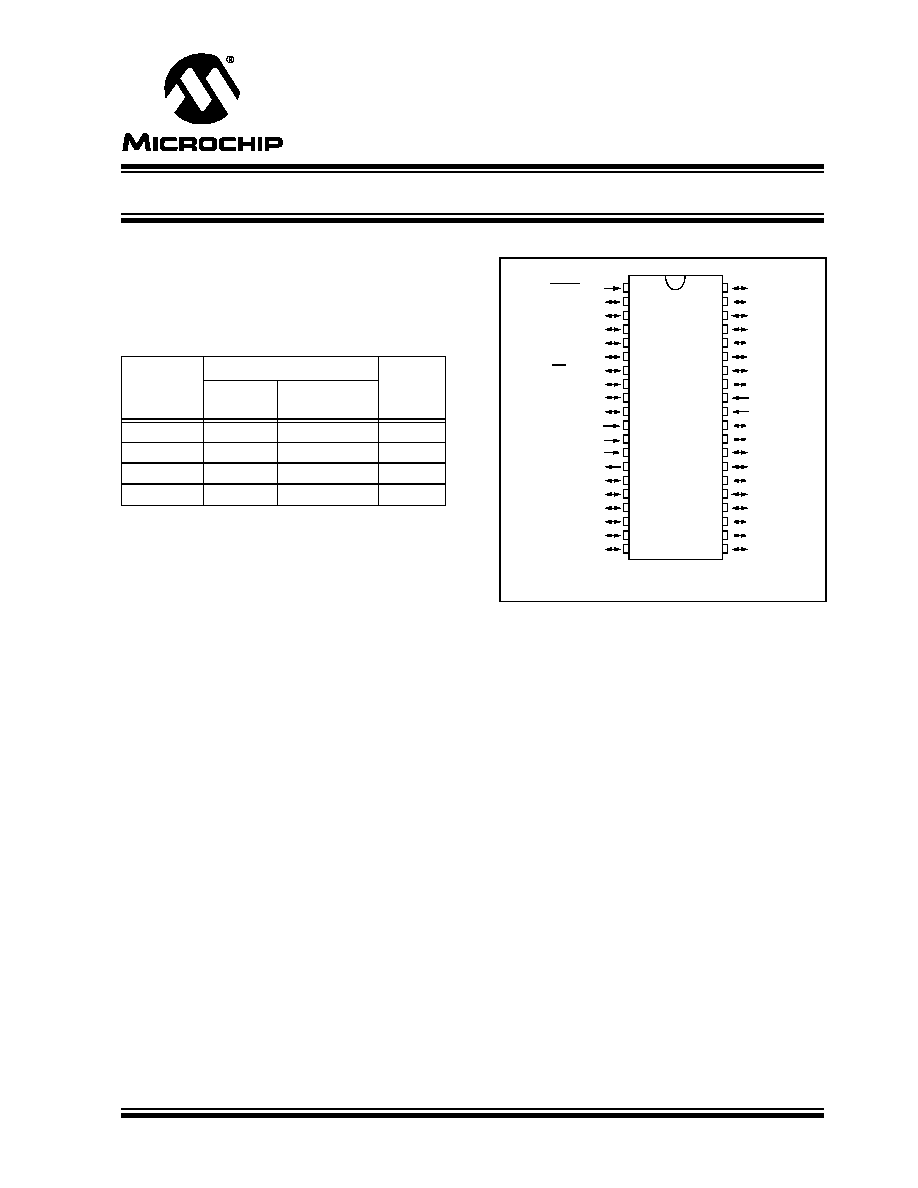
Pin Diagrams
Analog Features:
∑ 10-bit Analog-to-Digital Converter module (A/D)
with:
-
Fast sampling rate
-
Conversion available during sleep
-
DNL = ±1 LSb, INL = ±1 LSb
∑ Programmable Low-Voltage Detection (LVD)
module
-
Supports interrupt on low voltage detection
∑ Programmable Brown-out Reset (BOR)
Special Microcontroller Features:
∑ Power-on Reset (POR), Power-up Timer (PWRT)
and Oscillator Start-up Timer (OST)
∑ Watchdog Timer (WDT) with its own on-chip RC
oscillator for reliable operation
∑ Programmable code-protection
∑ Power saving SLEEP mode
∑ Selectable oscillator options including:
-
4X Phase Lock Loop (of primary oscillator)
-
Secondary Oscillator (32 kHz) clock input
∑ In-Circuit Serial Programming (ICSPTM) via two pins
CMOS Technology:
∑ Low-power, high-speed EPROM technology
∑ Fully static design
∑ Wide operating voltage range (2.5V to 5.5V)
∑ Industrial and Extended temperature ranges
∑ Low-power consumption
Device
On-Chip Program Memory On-Chip
RAM
(bytes)
EPROM
(bytes)
# Single Word
Instructions
PIC18C242
16K
8192
512
PIC18C252
32K
16384
1536
PIC18C442
16K
8192
512
PIC18C452
32K
16384
1536
*
*
*
*
*
RB7
RB6
RB5
RB4
RB3/CCP2
*
RB2/INT2
RB1/INT1
RB0/INT0
V
DD
V
SS
RD7/PSP7
RD6/PSP6
RD5/PSP5
RD4/PSP4
RC7/RX/DT
RC6/TX/CK
RC5/SDO
RC4/SDI/SDA
RD3/PSP3
RD2/PSP2
MCLR/V
PP
RA0/AN
0
RA1/AN1
RA2/AN2/V
REF
-
RA3/AN3/V
REF
+
RA4/T0CKI
RA5/AN4/SS/LVDIN
RE0/RD/AN5
RE1/WR/AN6
RE2/CS/AN7
V
DD
V
SS
OSC1/CLKI
OSC2/CLKO/RA6
RC0/T1OSO/T1CKI
RC1/T1OSI/CCP2
*
RC2/CCP1
RC3/SCK/SCL
RD0/PSP0
RD1/PSP1
1
2
3
4
5
6
7
8
9
10
11
12
13
14
15
16
17
18
19
20
40
39
38
37
36
35
34
33
32
31
30
29
28
27
26
25
24
23
22
21
PI
C
1
8C
4
X
2
*
RB3 is the alternate pin for the CCP2 pin multiplexing.
DIP, Windowed CERDIP
NOTE: Pin compatible with 40-pin PIC16C7X devices
PIC18CXX2
High-Performance Microcontrollers with 10-Bit A/D
DS39026B-page 2
Preliminary
©
7/99 Microchip Technology Inc.
PIC18CXX2
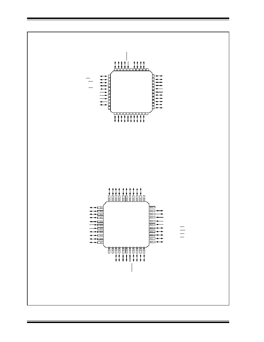
Pin Diagrams
10
11
12
13
14
15
16
1718
19
20
21
22
23 24
25
26
44
8
7
6
5
4
3
2
1
27
28 29
30
31
32
33
34
35
36
37
38
39
40
41
42
43
9
PIC18C4X2
RA4/T0CKI
RA5/AN4/SS/LVDIN
RE0/RD/AN5
OSC2/CLKO/RA6
NC
RE1/WR/AN6
RE2/CS/AN7
V
DD
OSC1/CLKI
RB3/CCP2
*
RB2/INT2
RB1/INT1
RB0/INT0
V
DD
V
SS
RD7/PSP7
RD6/PSP6
RD5/PSP5
RD4/PSP4
RC7/RX/DT
RA3
/
AN3
/
V
RE
F
+
RA2
/
AN2
/
V
RE
F
-
RA1
/
AN1
RA0
/
AN0
MC
L
R
/V
PP
NC
RB7
RB6
RB5
RB4
NC
NC
RC6
/T
X/CK
RC5
/SDO
RC4
/SDI/
S
D
A
RD3
/
PSP3
RD2
/
PSP2
RD1
/
PSP1
RD0
/
PSP0
RC3
/SCK/SCL
RC2
/CCP1
RC1
/T
1
O
S
I
/CCP2
*
10
11
2
3
4
5
6
1
18
19
20
21
22
12
13
14
15
38
8
7
44
43
42
41
40
39
16
17
29
30
31
32
33
23
24
25
26
27
28
36
34
35
9
PIC18C4X2
37
RA3
/
AN3
/
V
RE
F
+
RA2
/
AN2
/
V
RE
F
-
RA1
/
AN1
RA0
/
AN0
MC
L
R
/V
PP
NC
RB7
RB6
RB5
RB4
NC
RC6
/T
X/CK
RC5
/SDO
RC4
/S
DI/S
D
A
RD3
/
PSP3
RD2
/
PSP2
RD1
/
PSP1
RD0
/
PSP0
RC3
/SCK/SCL
RC2
/CCP1
RC1
/T
1
O
SI/
CCP2
*
NC
NC
RC0/T1OSO/T1CKI
OSC2/CLKO/RA6
OSC1/CLKI
V
SS
V
DD
RE2/AN7/CS
RE1/AN6/WR
RE0/AN5/RD
RA5/AN4/SS/LVDIN
RA4/T0CKI
RC7/RX/DT
RD4/PSP4
RD5/PSP5
RD6/PSP6
RD7/PSP7
V
SS
V
DD
RB0/INT0
RB1/INT1
RB2/INT2
RB3/CCP2
*
PLCC
TQFP
*
RB3 is the alternate pin for the CCP2 pin multiplexing.
NOTE: Pin compatible with 44-pin PIC16C7X devices
V
SS
RC0/T1OSO/T1CKI
PIC18CXX2
©
7/99 Microchip Technology Inc.
Preliminary
DS39026B-page 3
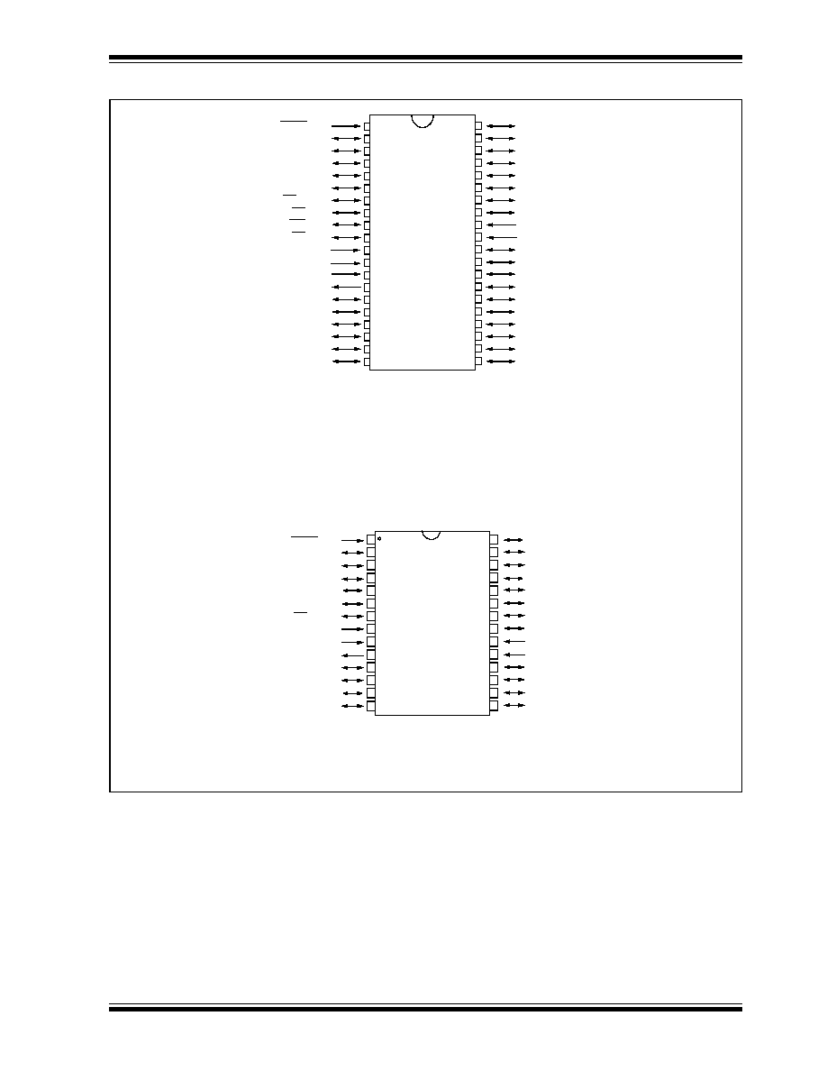
Pin Diagrams (Cont.'d)
RB7
RB6
RB5
RB4
RB3/CCP2
*
RB2/INT2
RB1/INT1
RB0/INT0
V
DD
V
SS
RD7/PSP7
RD6/PSP6
RD5/PSP5
RD4/PSP4
RC7/RX/DT
RC6/TX/CK
RC5/SDO
RC4/SDI/SDA
RD3/PSP3
RD2/PSP2
MCLR/V
PP
RA0/AN0
RA1/AN1
RA2/AN2/V
REF
-
RA3/AN3/V
REF
+
RA4/T0CKI
RA5/AN4/SS/LVDIN
RE0/RD/AN5
RE1/WR/AN6
RE2/CS/AN7
V
DD
V
SS
OSC1/CLKI
OSC2/CLKO/RA6
RC0/T1OSO/T1CKI
RC1/T1OSI/CCP2
*
RC2/CCP1
RC3/SCK/SCL
RD0/PSP0
RD1/PSP1
1
2
3
4
5
6
7
8
9
10
11
12
13
14
15
16
17
18
19
20
40
39
38
37
36
35
34
33
32
31
30
29
28
27
26
25
24
23
22
21
PI
C18C
4X2
PI
C
1
8C
2
X
2
10
11
2
3
4
5
6
1
8
7
9
12
13
14
15
16
17
18
19
20
23
24
25
26
27
28
22
21
MCLR/V
PP
RA0/AN0
RA1/AN1
RA2/AN2/V
REF
-
RA3/AN3/V
REF
+
RA4/T0CKI
RA5/AN4/SS/LVDIN
V
SS
OSC1/CLKI
OSC2/CLKO/RA6
RC0/T1OSO/T1CKI
RC1/T1OSI/CCP2
*
RC2/CCP1
RC3/SCK/SCL
RB7
RB6
RB5
RB4
RB3/CCP2
*
RB2/INT2
RB1/INT1
RB0/INT0
V
DD
V
SS
RC7/RX/DT
RC6/TX/CK
RC5/SDO
RC4/SDI/SDA
*
RB3 is the alternate pin for the CCP2 pin multiplexing.
DIP, JW
DIP, SOIC, JW
NOTE: Pin compatible with 40-pin PIC16C7X devices
NOTE: Pin compatible with 28-pin PIC16C7X devices

DS39026B-page 4
Preliminary
©
7/99 Microchip Technology Inc.
PIC18CXX2
Table of Contents
1.0
Device Overview .......................................................................................................................................................................... 5
2.0
Oscillator Configurations ............................................................................................................................................................ 15
3.0
Reset .......................................................................................................................................................................................... 23
4.0
Memory Organization ................................................................................................................................................................. 33
5.0
Table Reads/Table Writes .......................................................................................................................................................... 53
6.0
8 X 8 Hardware Multiplier ........................................................................................................................................................... 61
7.0
Interrupts .................................................................................................................................................................................... 65
8.0
I/O Ports ..................................................................................................................................................................................... 77
9.0
Timer0 Module ........................................................................................................................................................................... 93
10.0 Timer1 Module ........................................................................................................................................................................... 97
11.0 Timer2 Module ......................................................................................................................................................................... 102
12.0 Timer3 Module ......................................................................................................................................................................... 105
13.0 Capture/Compare/PWM (CCP) Modules ................................................................................................................................. 109
14.0 Master Synchronous Serial Port (MSSP) Module .................................................................................................................... 117
15.0 Addressable Universal Synchronous Asynchronous Receiver Transmitter (USART).............................................................. 151
16.0 10-bit Analog-to-Digital Converter (A/D) Module ...................................................................................................................... 167
17.0 Low Voltage Detect .................................................................................................................................................................. 175
18.0 Special Features of the CPU .................................................................................................................................................... 181
19.0 Instruction Set Summary .......................................................................................................................................................... 191
20.0 Development Support............................................................................................................................................................... 235
21.0 Electrical Characteristics .......................................................................................................................................................... 241
22.0 DC and AC Characteristics Graphs and Tables ....................................................................................................................... 273
23.0 Packaging Information.............................................................................................................................................................. 275
Appendix A:
Revision History ......................................................................................................................................................... 283
Appendix B:
Device Differences..................................................................................................................................................... 283
Appendix C:
Conversion Considerations........................................................................................................................................ 284
Appendix D:
Migration from Baseline to Enhanced Devices .......................................................................................................... 284
Appendix E:
Migration from Midrange to Enhanced Devices ......................................................................................................... 285
Appendix F:
Migration from High-end to Enhanced Devices ......................................................................................................... 285
Index ................................................................................................................................................................................................. 287
On-Line Support................................................................................................................................................................................. 293
Reader Response .............................................................................................................................................................................. 294
PIC18CXX2 Product Identification System ........................................................................................................................................ 295
To Our Valued Customers
Most Current Data Sheet
To obtain the most up-to-date version of this data sheet, please register at our Worldwide Web site at:
http://www.microchip.com
You can determine the version of a data sheet by examining its literature number found on the bottom outside corner of any page.
The last character of the literature number is the version number. e.g., DS30000A is version A of document DS30000.
New Customer Notification System
Register on our web site (www.microchip.com/cn) to receive the most current information on our products.
Errata
An errata sheet may exist for current devices, describing minor operational differences (from the data sheet) and recommended
workarounds. As device/documentation issues become known to us, we will publish an errata sheet. The errata will specify the revi-
sion of silicon and revision of document to which it applies.
To determine if an errata sheet exists for a particular device, please check with one of the following:
∑ Microchip's Worldwide Web site; http://www.microchip.com
∑ Your local Microchip sales office (see last page)
∑ The Microchip Corporate Literature Center; U.S. FAX: (602) 786-7277
When contacting a sales office or the literature center, please specify which device, revision of silicon and data sheet (include liter-
ature number) you are using.
Corrections to this Data Sheet
We constantly strive to improve the quality of all our products and documentation. We have spent a great deal of time to ensure
that this document is correct. However, we realize that we may have missed a few things. If you find any information that is missing
or appears in error, please:
∑ Fill out and mail in the reader response form in the back of this data sheet.
∑ E-mail us at webmaster@microchip.com.
We appreciate your assistance in making this a better document.
©
7/99 Microchip Technology Inc.
Preliminary
DS39026B-page 5
PIC18CXX2
1.0
DEVICE OVERVIEW
This document contains device-specific information for
the following four devices:
1.
PIC18C242
2.
PIC18C252
3.
PIC18C442
4.
PIC18C452
These devices come in 28 and 40-pin packages. The
28-pin devices do not have a Parallel Slave Port (PSP)
implemented and the number of Analog-to-Digital (A/D)
converter input channels is reduced to 5. An overview
of features is shown in Table 1-1.
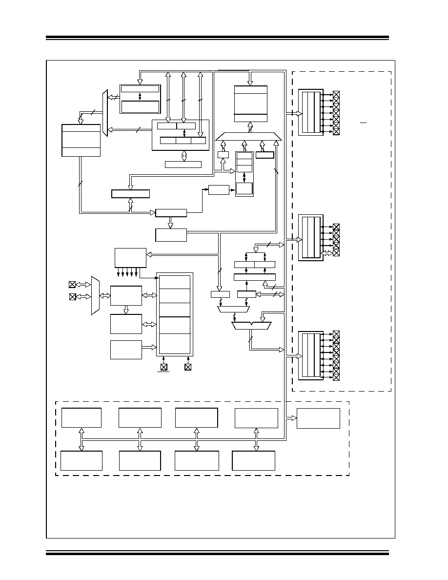
The following two figures are device block diagrams
sorted by pin count; 28-pin for Figure 1-1 and 40-pin for
Figure 1-2. The 28-pin and 40-pin pinouts are listed in
Table 1-2 and Table 1-3 respectively.
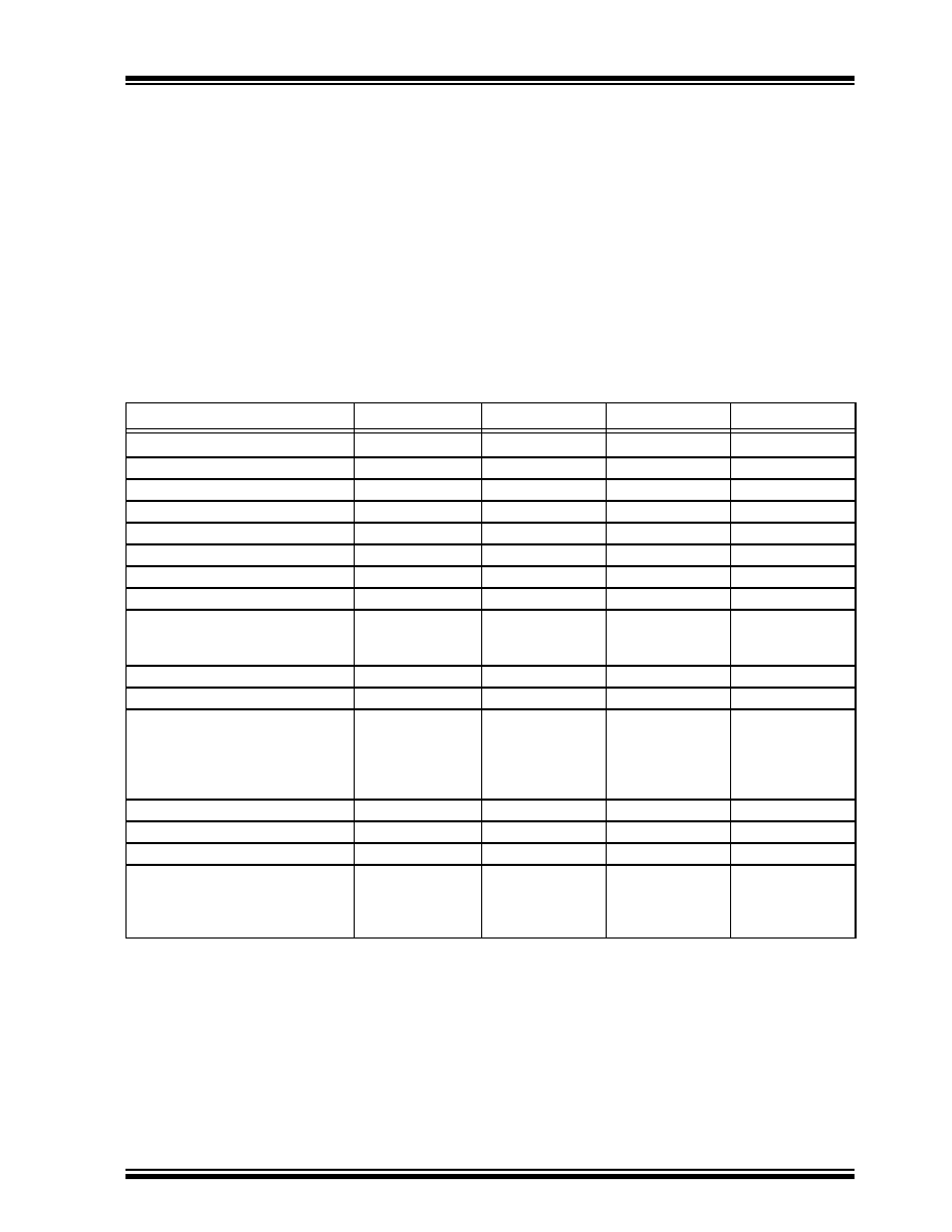
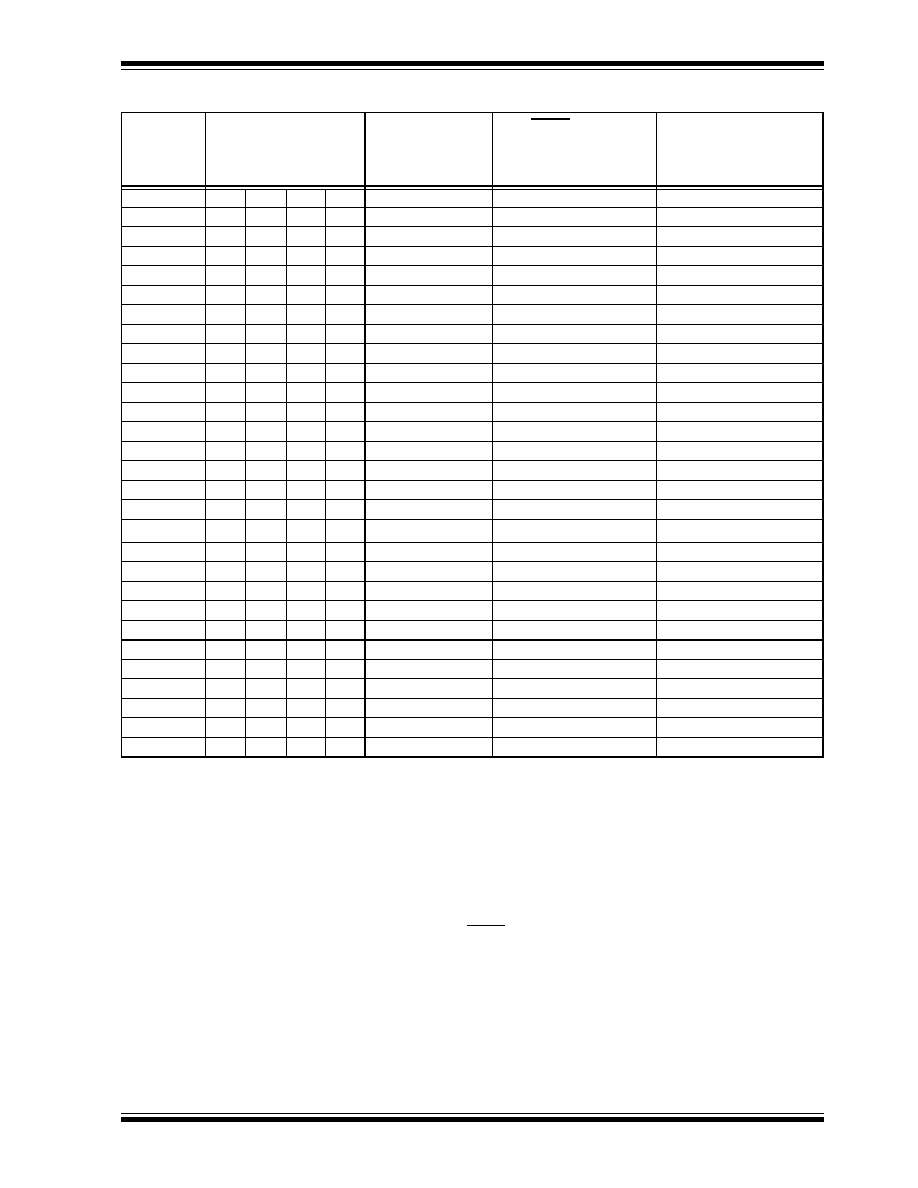
TABLE 1-1:
DEVICE FEATURES
Features
PIC18C242
PIC18C252
PIC18C442
PIC18C452
Operating Frequency
DC - 40 MHz
DC - 40 MHz
DC - 40 MHz
DC - 40 MHz
Program Memory (Bytes)
16K
32K
16K
32K
Program Memory (Instructions)
8192
16384
8192
16384
Data Memory (Bytes)
512
1536
512
1536
Interrupt sources
16
16
17
17
I/O Ports
Ports A, B, C
Ports A, B, C
Ports A, B, C, D, E Ports A, B, C, D, E
Timers
4
4
4
4
Capture/Compare/PWM modules
2
2
2
2
Serial Communications
MSSP,
Addressable
USART
MSSP,
Addressable
USART
MSSP,
Addressable
USART
MSSP,
Addressable
USART
Parallel Communications
--
--
PSP
PSP
10-bit Analog-to-Digital Module
5 input channels
5 input channels
8 input channels
8 input channels
Resets (and Delays)
POR, BOR,
Reset Instruction,
Stack Full,
Stack Underflow
(PWRT, OST)
POR, BOR,
Reset Instruction,
Stack Full,
Stack Underflow
(PWRT, OST)
POR, BOR,
Reset Instruction,
Stack Full,
Stack Underflow
(PWRT, OST)
POR, BOR,
Reset Instruction,
Stack Full,
Stack Underflow
(PWRT, OST)
Programmable Low Voltage Detect
Yes
Yes
Yes
Yes
Programmable Brown-out Reset
Yes
Yes
Yes
Yes
Instruction Set
75 Instructions
75 Instructions
75 Instructions
75 Instructions
Packages
28-pin DIP
28-pin SOIC
28-pin JW
28-pin DIP
28-pin SOIC
28-pin JW
40-pin DIP
40-pin PLCC
40-pin TQFP
40-pin JW
40-pin DIP
40-pin PLCC
40-pin TQFP
40-pin JW
PIC18CXX2
DS39026B-page 6
Preliminary
©
7/99 Microchip Technology Inc.
FIGURE 1-1:
PIC18C2X2 BLOCK DIAGRAM
Power-up
Timer
Oscillator
Start-up Timer
Power-on
Reset
Watchdog
Timer
Instruction
Decode &
Control
OSC1/CLKI
OSC2/CLKO
MCLR
V
DD
, V
SS
PORTA
PORTB
PORTC
RA4/T0CKI
RA5/AN4/SS/LVDIN
RB0/INT0
RB7:RB4
RC0/T1OSO/T1CKI
RC1/T1OSI/CCP2
(1)
RC2/CCP1
RC3/SCK/SCL
RC4/SDI/SDA
RC5/SDO
RC6/TX/CK
RC7/RX/DT
Brown-out
Reset
Note 1: Optional multiplexing of CCP2 input/output with RB3 is enabled by selection of configuration bit.
2: The high order bits of the Direct Address for the RAM are from the BSR register (except for the MOVFF
instruction).
3: Many of the general purpose I/O pins are multiplexed with one or more peripheral module functions. The
multiplexing combinations are device dependent.
Addressable
CCP1
Synchronous
Timer0
Timer1
Timer2
Serial Port
RA3/AN3/V
REF
+
RA2/AN2/V
REF
-
RA1/AN1
RA0/AN0
Timing
Generation
4X PLL
A/D Converter
Precision
Reference
RB1/INT1
Data Latch
Data RAM
Address Latch
Address<12>
12
(2)
BSR
FSR0
FSR1
FSR2
4
12
4
PCH
PCL
PCLATH
8
31 Level Stack
Program Counter
PRODL
PRODH
8 x 8 Multiply
WREG
8
BIT OP
8
8
ALU<8>
8
Address Latch
Program Memory
(up to 2M Bytes)
Data Latch
20
21
21
16
8
8
8
inc/dec logic
21
8
Data Bus<8>
8
Instruction
12
3
ROMLATCH
Timer3
CCP2
RB2/INT2
RB3/CCP2
(1)
T1OSI
T1OSO
Bank0, F
PCLATU
PCU
RA6
Voltage
USART
Master
8
Register
TABLELATCH
Table Pointer <2>
inc/dec
logic
Decode
©
7/99 Microchip Technology Inc.
Preliminary
DS39026B-page 7
PIC18CXX2
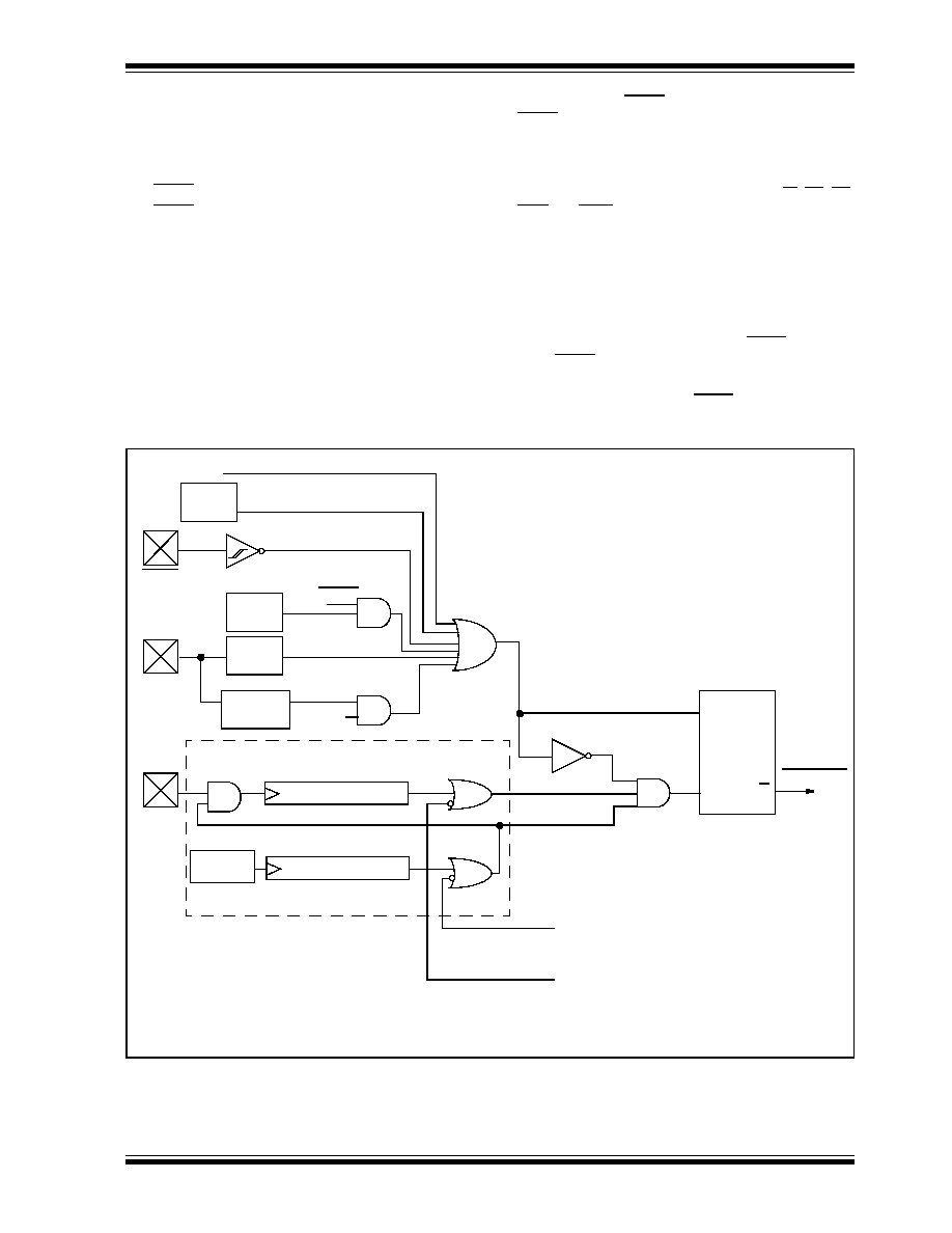
FIGURE 1-2:
PIC18C4X2 BLOCK DIAGRAM
Power-up
Timer
Oscillator
Start-up Timer
Power-on
Reset
Watchdog
Timer
Instruction
Decode &
Control
OSC1/CLKI
OSC2/CLKO
MCLR
V
DD
, V
SS
PORTA
PORTB
PORTC
RA4/T0CKI
RA5/AN4/SS/LVDIN
RB0/INT0
RB7:RB4
RC0/T1OSO/T1CKI
RC1/T1OSI/CCP2
(1)
RC2/CCP1
RC3/SCK/SCL
RC4/SDI/SDA
RC5/SDO
RC6/TX/CK
RC7/RX/DT
Brown-out
Reset
Note 1: Optional multiplexing of CCP2 input/output with RB3 is enabled by selection of configuration bit.
2: The high order bits of the Direct Address for the RAM are from the BSR register (except for the MOVFF
instruction).
3: Many of the general purpose I/O pins are multiplexed with one or more peripheral module functions.
The multiplexing combinations are device dependent.
Addressable
CCP1
Master
Timer0
Timer1
Timer2
Serial Port
RA3/AN3/V
REF
+
RA2/AN2/V
REF
-
RA1/AN1
RA0/AN0
Parallel Slave Port
Timing
Generation
4X PLL
A/D Converter
RB1/INT1
Data Latch
Data RAM
(up to 4K
address reach)
Address Latch
Address<12>
12
(2)
Bank0, F
BSR
FSR0
FSR1
FSR2
4
12
4
PCH PCL
PCLATH
8
31 Level Stack
Program Counter
PRODL
PRODH
8 x 8 Multiply
WREG
8
BIT OP
8
8
ALU<8>
8
Address Latch
Program Memory
(up to 2M Bytes)
Data Latch
20
21
21
16
8
8
8
inc/dec logic
21
8
Data Bus<8>
TABLELATCH
8
Instruction
12
3
ROMLATCH
Timer3
PORTD
PORTE
RD7/PSP7:RD0/PSP0
RE0/AN5/RD
RE1/AN6/WR
RE2/AN7/CS
CCP2
RB2/INT2
RB3/CCP2
(1)
T1OSI
T1OSO
PCLATU
PCU
RA6
Precision
Reference
Voltage
Synchronous
USART
Register
8
Table Pointer <2>
inc/dec
logic
Decode
PIC18CXX2
DS39026B-page 8
Preliminary
©
7/99 Microchip Technology Inc.
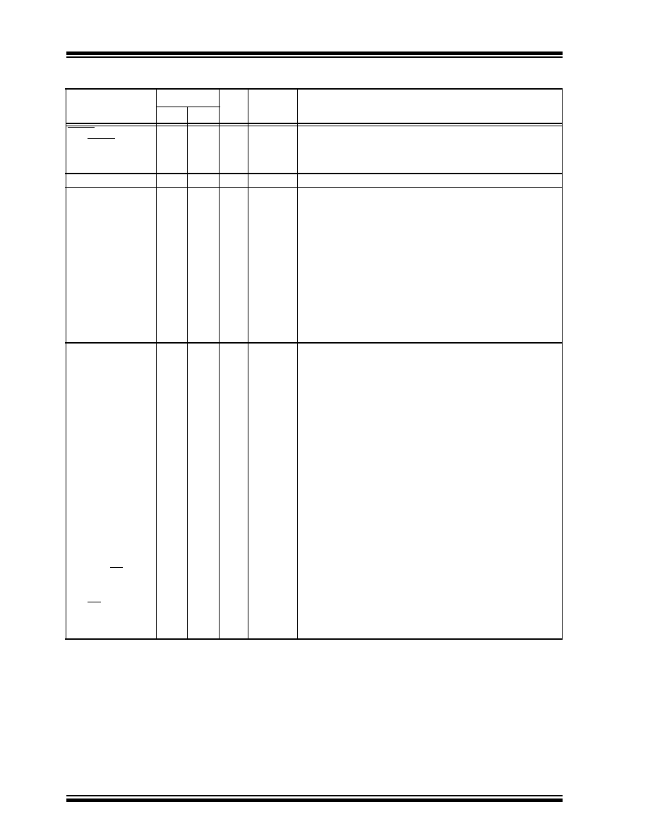
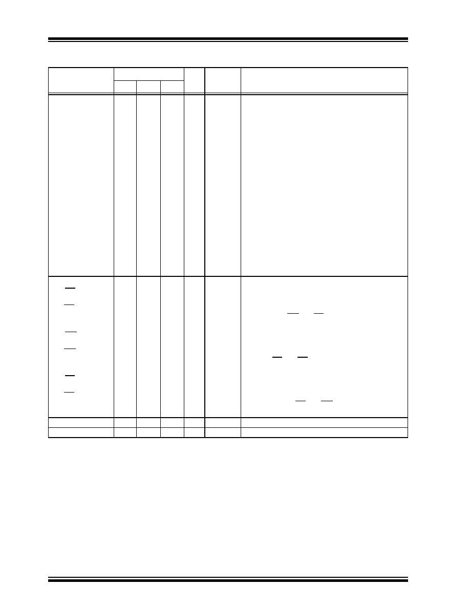
TABLE 1-2:
PIC18C2X2 PINOUT I/O DESCRIPTIONS
Pin Name
Pin Number
Pin
Type
Buffer
Type
DIP
SOIC
Description
MCLR/V
PP
MCLR
V
PP
1
1
I
P
ST
Master clear (reset) input. This pin is an active low reset
to the device.
Programming voltage input.
NC
--
--
--
--
These pins should be left unconnected.
OSC1/CLKI
OSC1
CLKI
9
9
I
I
ST
CMOS
Oscillator crystal input or external clock source input.
ST buffer when configured in RC mode. CMOS otherwise.
External clock source input. Always associated with
pin function OSC1. (See related OSC1/CLKIN,
OSC2/CLKOUT pins).
OSC2/CLKO/RA6
OSC2
CLKO
RA6
10
10
O
O
I/O
--
--
TTL
Oscillator crystal output. Connects to crystal or
resonator in crystal oscillator mode.
In RC mode, OSC2 pin outputs CLKOUT which has 1/4
the frequency of OSC1, and denotes the instruction
cycle rate.
General Purpose I/O pin.
PORTA is a bi-directional I/O port.
RA0/AN0
RA0
AN0
2
2
I/O
I
TTL
Analog
Digital I/O.
Analog input 0.
RA1/AN1
RA1
AN1
3
3
I/O
I
TTL
Analog
Digital I/O.
Analog input 1.
RA2/AN2/V
REF
-
RA2
AN2
V
REF
-
4
4
I/O
I
I
TTL
Analog
Analog
Digital I/O.
Analog input 2.
A/D Reference Voltage (Low) input.
RA3/AN3/V
REF
+
RA3
AN3
V
REF
+
5
5
I/O
I
I
TTL
Analog
Analog
Digital I/O.
Analog input 3.
A/D Reference Voltage (High) input.
RA4/T0CKI
RA4
T0CKI
6
6
I/O
I
ST/OD
ST
Digital I/O. Open drain when configured as output.
Timer0 external clock input.
RA5/AN4/SS/LVDIN
RA5
AN4
SS
LVDIN
7
7
I/O
I
I
I
TTL
Analog
ST
Analog
Digital I/O.
Analog input 4.
SPI Slave Select input.
Low Voltage Detect Input.
RA6
See the OSC2/CLKO/RA6 pin.
Legend: TTL = TTL compatible input
CMOS = CMOS compatible input or output
ST = Schmitt Trigger input with CMOS levels
I = Input
O = Output
P = Power
OD = Open Drain (no P diode to V
DD
)

©
7/99 Microchip Technology Inc.
Preliminary
DS39026B-page 9
PIC18CXX2
PORTB is a bi-directional I/O port. PORTB can be software
programmed for internal weak pull-ups on all inputs.
RB0/INT0
RB0
INT0
21
21
I/O
I
TTL
ST
Digital I/O.
External Interrupt 0.
RB1/INT1
RB1
INT1
22
22
I/O
I
TTL
ST
External Interrupt 1.
RB2/INT2
RB2
INT2
23
23
I/O
I
TTL
ST
Digital I/O.
External Interrupt 2.
RB3/CCP2
RB3
CCP2
24
24
I/O
I/O
TTL
ST
Digital I/O.
Capture2 input, Compare2 output, PWM2 output.
RB4
25
25
I/O
TTL
Digital I/O.
Interrupt on change pin.
RB5
26
26
I/O
TTL
Digital I/O.
Interrupt on change pin.
RB6
27
27
I/O
I
TTL
ST
Digital I/O.
Interrupt on change pin.
ICSP programming clock.
RB7
28
28
I/O
I/O
TTL
ST
Digital I/O.
Interrupt on change pin.
ICSP programming data.
TABLE 1-2:
PIC18C2X2 PINOUT I/O DESCRIPTIONS (Cont.'d)
Pin Name
Pin Number
Pin
Type
Buffer
Type
DIP
SOIC
Description
Legend: TTL = TTL compatible input
CMOS = CMOS compatible input or output
ST = Schmitt Trigger input with CMOS levels
I = Input
O = Output
P = Power
OD = Open Drain (no P diode to V
DD
)

PIC18CXX2
DS39026B-page 10
Preliminary
©
7/99 Microchip Technology Inc.
PORTC is a bi-directional I/O port.
RC0/T1OSO/T1CKI
RC0
T1OSO
T1CKI
11
11
I/O
O
I
ST
--
ST
Digital I/O.
Timer1 oscillator output.
Timer1/Timer3 external clock input.
RC1/T1OSI/CCP2
RC1
T1OSI
CCP2
12
12
I/O
I
I/O
ST
CMOS
ST
Digital I/O.
Timer1 oscillator input.
Capture2 input, Compare2 output, PWM2 output.
RC2/CCP1
RC2
CCP1
13
13
I/O
I/O
ST
ST
Digital I/O.
Capture1 input/Compare1 output/PWM1 output.
RC3/SCK/SCL
RC3
SCK
SCL
14
14
I/O
I/O
I/O
ST
ST
ST
Digital I/O.
Synchronous serial clock input/output for SPI mode.
Synchronous serial clock input/output for I
2
C mode
RC4/SDI/SDA
RC4
SDI
SDA
15
15
I/O
I
I/O
ST
ST
ST
Digital I/O.
SPI Data In.
I
2
C Data I/O.
RC5/SDO
RC5
SDO
16
16
I/O
O
ST
--
Digital I/O.
SPI Data Out.
RC6/TX/CK
RC6
TX
CK
17
17
I/O
O
I/O
ST
--
ST
Digital I/O.
USART Asynchronous Transmit.
USART Synchronous Clock.
(See related RX/DT)
RC7/RX/DT
RC7
RX
DT
18
18
I/O
I
I/O
ST
ST
ST
Digital I/O.
USART Asynchronous Receive.
USART Synchronous Data.
(See related TX/CK)
V
SS
8, 19
8, 19
P
--
Ground reference for logic and I/O pins.
V
DD
20
20
P
--
Positive supply for logic and I/O pins.
TABLE 1-2:
PIC18C2X2 PINOUT I/O DESCRIPTIONS (Cont.'d)
Pin Name
Pin Number
Pin
Type
Buffer
Type
DIP
SOIC
Description
Legend: TTL = TTL compatible input
CMOS = CMOS compatible input or output
ST = Schmitt Trigger input with CMOS levels
I = Input
O = Output
P = Power
OD = Open Drain (no P diode to V
DD
)
©
7/99 Microchip Technology Inc.
Preliminary
DS39026B-page 11
PIC18CXX2
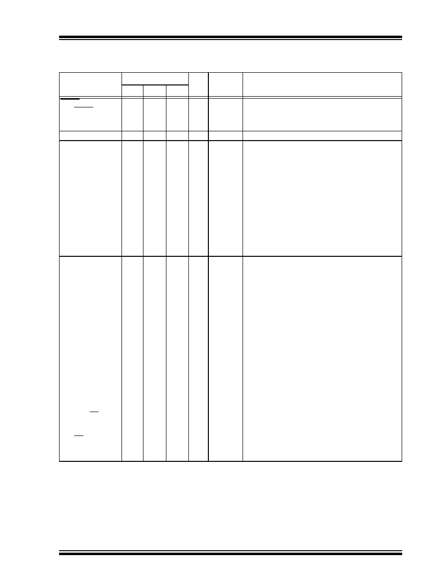
TABLE 1-3:
PIC18C4X2 PINOUT I/O DESCRIPTIONS
Pin Name
Pin Number
Pin
Type
Buffer
Type
DIP
PLCC TQFP
Description
MCLR/V
PP
MCLR
V
PP
1
2
18
I
P
ST
Master clear (reset) input. This pin is an active
low reset to the device.
Programming voltage input.
NC
--
--
--
These pins should be left unconnected.
OSC1/CLKI
OSC1
CLKI
13
14
30
I
I
ST
CMOS
Oscillator crystal input or external clock
source input. ST buffer when configured in
RC mode. CMOS otherwise.
External clock source input. Always
associated with pin function OSC1. (See
related OSC1/CLKIN, OSC2/CLKOUT pins).
OSC2/CLKO/RA6
OSC2
CLKO
RA6
14
15
31
O
O
I/O
--
--
TTL
Oscillator crystal output. Connects to crystal
or resonator in crystal oscillator mode.
In RC mode, OSC2 pin outputs CLKOUT,
which has 1/4 the frequency of OSC1 and
denotes the instruction cycle rate.
General Purpose I/O pin.
PORTA is a bi-directional I/O port.
RA0/AN0
RA0
AN0
2
3
19
I/O
I
TTL
Analog
Digital I/O.
Analog input 0.
RA1/AN1
RA1
AN1
3
4
20
I/O
I
TTL
Analog
Digital I/O.
Analog input 1.
RA2/AN2/V
REF
-
RA2
AN2
V
REF
-
4
5
21
I/O
I
I
TTL
Analog
Analog
Digital I/O.
Analog input 2.
A/D Reference Voltage (Low) input.
RA3/AN3/V
REF
+
RA3
AN3
V
REF
+
5
6
22
I/O
I
I
TTL
Analog
Analog
Digital I/O.
Analog input 3.
A/D Reference Voltage (High) input.
RA4/T0CKI
RA4
T0CKI
6
7
23
I/O
I
ST/OD
ST
Digital I/O. Open drain when configured as output.
Timer0 external clock input.
RA5/AN4/SS/LVDIN
RA5
AN4
SS
LVDIN
7
8
24
I/O
I
I
I
TTL
Analog
ST
Analog
Digital I/O.
Analog input 4.
SPI Slave Select input.
Low Voltage Detect Input.
RA6
See the OSC2/CLKO/RA6 pin.
Legend: TTL = TTL compatible input
CMOS = CMOS compatible input or output
ST = Schmitt Trigger input with CMOS levels
I = Input
O = Output
P = Power
OD = Open Drain (no P diode to V
DD
)

PIC18CXX2
DS39026B-page 12
Preliminary
©
7/99 Microchip Technology Inc.
PORTB is a bi-directional I/O port. PORTB can be
software programmed for internal weak pull-ups on all
inputs.
RB0/INT0
RB0
INT0
33
36
8
I/O
I
TTL
ST
Digital I/O.
External Interrupt 0.
RB1/INT1
RB1
INT1
34
37
9
I/O
I
TTL
ST
External Interrupt 1.
RB2/INT2
RB2
INT2
35
38
10
I/O
I
TTL
ST
Digital I/O.
External Interrupt 2.
RB3/CCP2
RB3
CCP2
36
39
11
I/O
I/O
TTL
ST
Digital I/O.
Capture2 input, Compare2 output, PWM2 output.
RB4
37
41
14
I/O
TTL
Digital I/O.
Interrupt on change pin.
RB5
38
42
15
I/O
TTL
Digital I/O.
Interrupt on change pin.
RB6
39
43
16
I/O
I
TTL
ST
Digital I/O.
Interrupt on change pin.
ICSP programming clock.
RB7
40
44
17
I/O
I/O
TTL
ST
Digital I/O.
Interrupt on change pin.
ICSP programming data.
TABLE 1-3:
PIC18C4X2 PINOUT I/O DESCRIPTIONS (Cont.'d)
Pin Name
Pin Number
Pin
Type
Buffer
Type
DIP
PLCC TQFP
Description
Legend: TTL = TTL compatible input
CMOS = CMOS compatible input or output
ST = Schmitt Trigger input with CMOS levels
I = Input
O = Output
P = Power
OD = Open Drain (no P diode to V
DD
)

©
7/99 Microchip Technology Inc.
Preliminary
DS39026B-page 13
PIC18CXX2
PORTC is a bi-directional I/O port.
RC0/T1OSO/T1CKI
RC0
T1OSO
T1CKI
15
16
32
I/O
O
I
ST
--
ST
Digital I/O.
Timer1 oscillator output.
Timer1/Timer3 external clock input.
RC1/T1OSI/CCP2
RC1
T1OSI
CCP2
16
18
35
I/O
I
I/O
ST
CMOS
ST
Digital I/O.
Timer1 oscillator input.
Capture2 input, Compare2 output, PWM2 output.
RC2/CCP1
RC2
CCP1
17
19
36
I/O
I/O
ST
ST
Digital I/O.
Capture1 input/Compare1 output/PWM1 output.
RC3/SCK/SCL
RC3
SCK
SCL
18
20
37
I/O
I/O
I/O
ST
ST
ST
Digital I/O.
Synchronous serial clock input/output for
SPI mode.
Synchronous serial clock input/output for
I
2
C mode.
RC4/SDI/SDA
RC4
SDI
SDA
23
25
42
I/O
I
I/O
ST
ST
ST
Digital I/O.
SPI Data In.
I
2
C Data I/O.
RC5/SDO
RC5
SDO
24
26
43
I/O
O
ST
--
Digital I/O.
SPI Data Out.
RC6/TX/CK
RC6
TX
CK
25
27
44
I/O
O
I/O
ST
--
ST
Digital I/O.
USART Asynchronous Transmit.
USART Synchronous Clock.
(See related RX/DT)
RC7/RX/DT
RC7
RX
DT
26
29
1
I/O
I
I/O
ST
ST
ST
Digital I/O.
USART Asynchronous Receive.
USART Synchronous Data.
(See related TX/CK)
TABLE 1-3:
PIC18C4X2 PINOUT I/O DESCRIPTIONS (Cont.'d)
Pin Name
Pin Number
Pin
Type
Buffer
Type
DIP
PLCC TQFP
Description
Legend: TTL = TTL compatible input
CMOS = CMOS compatible input or output
ST = Schmitt Trigger input with CMOS levels
I = Input
O = Output
P = Power
OD = Open Drain (no P diode to V
DD
)
PIC18CXX2
DS39026B-page 14
Preliminary
©
7/99 Microchip Technology Inc.
PORTD is a bi-directional I/O port.
Parallel Slave Port (PSP) for interfacing to a micropro-
cessor port. These pins have TTL input buffers when
PSP module is enabled.
RD0/PSP0
19
21
38
I/O
ST
TTL
Digital I/O.
Parallel Slave Port Data.
RD1/PSP1
20
22
39
I/O
ST
TTL
Digital I/O.
Parallel Slave Port Data.
RD2/PSP2
21
23
40
I/O
ST
TTL
Digital I/O.
Parallel Slave Port Data.
RD3/PSP3
22
24
41
I/O
ST
TTL
Digital I/O.
Parallel Slave Port Data.
RD4/PSP4
27
30
2
I/O
ST
TTL
Digital I/O.
Parallel Slave Port Data.
RD5/PSP5
28
31
3
I/O
ST
TTL
Digital I/O.
Parallel Slave Port Data.
RD6/PSP6
29
32
4
I/O
ST
TTL
Digital I/O.
Parallel Slave Port Data.
RD7/PSP7
30
33
5
I/O
ST
TTL
Digital I/O.
Parallel Slave Port Data.
PORTE is a bi-directional I/O port.
RE0/RD/AN5
RE0
RD
AN5
8
9
25
I/O
ST
TTL
Analog
Digital I/O.
Read control for parallel slave port.
(See also WR and CS pins)
Analog input 5.
RE1/WR/AN6
RE1
WR
AN6
9
10
26
I/O
ST
TTL
Analog
Digital I/O.
Write control for parallel slave port.
(See CS and RD pins)
Analog input 6.
RE2/CS/AN7
RE2
CS
AN7
10
11
27
I/O
ST
TTL
Analog
Digital I/O.
Chip Select control for parallel slave port.
(See related RD and WR)
Analog input 7.
V
SS
12, 31 13, 34 6, 29
P
--
Ground reference for logic and I/O pins.
V
DD
11, 32 12, 35 7, 28
P
--
Positive supply for logic and I/O pins.
TABLE 1-3:
PIC18C4X2 PINOUT I/O DESCRIPTIONS (Cont.'d)
Pin Name
Pin Number
Pin
Type
Buffer
Type
DIP
PLCC TQFP
Description
Legend: TTL = TTL compatible input
CMOS = CMOS compatible input or output
ST = Schmitt Trigger input with CMOS levels
I = Input
O = Output
P = Power
OD = Open Drain (no P diode to V
DD
)
PIC18CXX2
©
7/99 Microchip Technology Inc.
Preliminary
DS39026B-page 15
2.0
OSCILLATOR
CONFIGURATIONS
2.1
Oscillator Types
The PIC18CXX2 can be operated in eight different
oscillator modes. The user can program three configu-
ration bits (FOSC2, FOSC1, and FOSC0) to select one
of these eight modes:
1.
LP
Low Power Crystal
2.
XT
Crystal/Resonator
3.
HS
High Speed Crystal/Resonator
4.
HS + PLL High Speed Crystal/Resonator with
PLL enabled
5.
RC
External Resistor/Capacitor
6.
RCIO
External Resistor/Capacitor with
I/O pin enabled
7.
EC
External Clock
8.
ECIO
External Clock with I/O pin enabled
2.2
Crystal Oscillator/Ceramic
Resonators
In XT, LP, HS or HS-PLL oscillator modes, a crystal or
ceramic resonator is connected to the OSC1 and
OSC2 pins to establish oscillation. Figure 2-1 shows
the pin connections. An external clock source may also
be connected to the OSC1 pin in these modes, as
shown in Figure 2-2.
The PIC18CXX2 oscillator design requires the use of a
parallel cut crystal.
FIGURE 2-1:
CRYSTAL/CERAMIC
RESONATOR OPERATION
(HS, XT OR LP
OSC CONFIGURATION)
FIGURE 2-2:
EXTERNAL CLOCK INPUT
OPERATION (HS, XT OR LP
OSC CONFIGURATION)
Note:
Use of a series cut crystal may give a fre-
quency out of the crystal manufacturers
specifications.
Note 1: See Table 2-1 and Table 2-2 for recom-
mended values of C1 and C2.
Note 2: A series resistor (R
S
) may be required
for AT strip cut crystals.
Note 3: R
F
varies with the crystal chosen.
C1
(1)
C2
(1)
XTAL
OSC2
OSC1
R
F
(3)
SLEEP
To
logic
PIC18CXXX
R
S
(2)
internal
OSC1
OSC2
Open
Clock from
ext. system
PIC18CXXX
PIC18CXX2
DS39026B-page 16
Preliminary
©
7/99 Microchip Technology Inc.
TABLE 2-1:
CERAMIC RESONATORS
TABLE 2-2:
CAPACITOR SELECTION FOR
CRYSTAL OSCILLATOR
2.3
RC Oscillator
For timing insensitive applications, the "RC" and
"RCIO" device options offer additional cost savings.
The RC oscillator frequency is a function of the supply
voltage, the resistor (R
EXT
) and capacitor (C
EXT
) val-
ues and the operating temperature. In addition to this,
the oscillator frequency will vary from unit to unit due
to normal process parameter variation. Furthermore,
the difference in lead frame capacitance between
package types will also affect the oscillation frequency,
especially for low C
EXT
values. The user also needs to
take into account variation due to tolerance of external
R and C components used. Figure 2-3 shows how the
R/C combination is connected.
In the RC oscillator mode, the oscillator frequency
divided by 4 is available on the OSC2 pin. This signal
may be used for test purposes or to synchronize other
logic.
FIGURE 2-3:
RC OSCILLATOR MODE
The RCIO oscillator mode functions like the RC mode,
except that the OSC2 pin becomes an additional gen-
eral purpose I/O pin. The I/O pin becomes bit 6 of
PORTA (RA6).
2.4
External Clock Input
The EC and ECIO oscillator modes require an external
clock source to be connected to the OSC1 pin. The
feedback device between OSC1 and OSC2 is turned
off in these modes to save current. There is no oscilla-
tor startup time required after a Power-On-Reset or
after a recovery from SLEEP mode.
In the EC oscillator mode, the oscillator frequency
divided by 4 is available on the OSC2 pin. This signal
may be used for test purposes or to synchronize other
logic. Figure 2-4 shows the pin connections for the EC
oscillator mode.
Ranges Tested:
Mode
Freq
OSC1
OSC2
XT
455 kHz
2.0 MHz
4.0 MHz
68 - 100 pF
15 - 68 pF
15 - 68 pF
68 - 100 pF
15 - 68 pF
15 - 68 pF
HS
8.0 MHz
16.0 MHz
10 - 68 pF
10 - 22 pF
10 - 68 pF
10 - 22 pF
These values are for design guidance only. See
notes at bottom of page.
Resonators Used:
455 kHz
Panasonic EFO-A455K04B
±
0.3%
2.0 MHz
Murata Erie CSA2.00MG
±
0.5%
4.0 MHz
Murata Erie CSA4.00MG
±
0.5%
8.0 MHz
Murata Erie CSA8.00MT
±
0.5%
16.0 MHz
Murata Erie CSA16.00MX
±
0.5%
All resonators used did not have built-in capacitors.
Osc Type
Crystal
Freq
Cap. Range
C1
Cap.
Range
C2
LP
32.0 kHz
33 pF
33 pF
200 kHz
15 pF
15 pF
XT
200 kHz
47-68 pF
47-68 pF
1.0 MHz
15 pF
15 pF
4.0 MHz
15 pF
15 pF
HS
4.0 MHz
15 pF
15 pF
8.0 MHz
15-33 pF
15-33 pF
20.0 MHz
15-33 pF
15-33 pF
25.0 MHz
TBD
TBD
These values are for design guidance only. See
notes at bottom of page.
Crystals Used
32.0 kHz
Epson C-001R32.768K-A
± 20 PPM
200 kHz
STD XTL 200.000KHz
± 20 PPM
1.0 MHz
ECS ECS-10-13-1
± 50 PPM
4.0 MHz
ECS ECS-40-20-1
± 50 PPM
8.0 MHz
EPSON CA-301 8.000M-C
± 30 PPM
20.0 MHz
EPSON CA-301 20.000M-C
± 30 PPM
Note 1: Recommended values of C1 and C2 are
identical to the ranges tested (Table 2-1).
2: Higher capacitance increases the stability
of the oscillator, but also increases the start-
up time.
3: Since each resonator/crystal has its own
characteristics, the user should consult the
resonator/crystal manufacturer for appropri-
ate values of external components.
4: Rs may be required in HS mode, as well as
XT mode, to avoid overdriving crystals with
low drive level specification.
OSC2/CLKO
C
EXT
R
EXT
PIC18CXXX
OSC1
F
OSC
/4
Internal
clock
V
DD
V
SS
Recommended values:
3 k
R
EXT
100 k
C
EXT
> 20pF
PIC18CXX2
©
7/99 Microchip Technology Inc.
Preliminary
DS39026B-page 17
FIGURE 2-4:
EXTERNAL CLOCK INPUT
OPERATION
(EC OSC CONFIGURATION)
The ECIO oscillator mode functions like the EC mode,
except that the OSC2 pin becomes an additional gen-
eral purpose I/O pin. The I/O pin becomes Bit 6 of
PORTA (RA6). Figure 2-5 shows the pin connections
for the ECIO oscillator mode.
FIGURE 2-5:
EXTERNAL CLOCK INPUT
OPERATION
(ECIO CONFIGURATION)
2.5
HS/PLL
A Phase Locked Loop circuit is provided as a program-
mable option for users that want to multiply the fre-
quency of the incoming crystal oscillator signal by 4.
For an input clock frequency of 10 MHz, the internal
clock frequency will be multiplied to 40 MHz. This is
useful for customers who are concerned with EMI due
to high frequency crystals.
The PLL can only be enabled when the oscillator con-
figuration bits are programmed for HS mode. If they
are programmed for any other mode, the PLL is not
enabled and the system clock will come directly from
OSC1.
The PLL is one of the modes of the FOSC<2:0> con-
figuration bits. The oscillator mode is specified during
device programming.
A PLL lock timer is used to ensure that the PLL has
locked before device execution starts. The PLL lock
timer has a time-out that is called T
PLL
.
FIGURE 2-6:
PLL BLOCK DIAGRAM
OSC1
OSC2
F
OSC
/4
Clock from
ext. system
PIC18CXXX
OSC1
I/O (OSC2)
RA6
Clock from
ext. system
PIC18CXXX
MUX
VCO
Loop
Filter
Divide by 4
Crystal
Osc
OSC2
OSC1
PLL Enable
F
IN
F
OUT
SYSCLK
Phase
Comparator
(from configuration
HS Osc
bit register)
PIC18CXX2
DS39026B-page 18
Preliminary
©
7/99 Microchip Technology Inc.
2.6
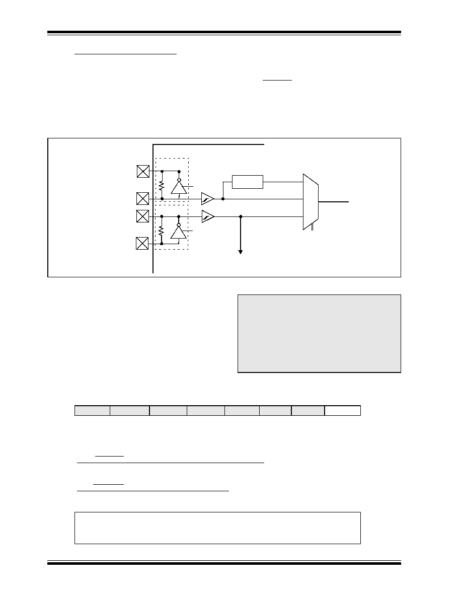
Oscillator Switching Feature
The PIC18CXX2 devices include a feature that allows
the system clock source to be switched from the main
oscillator to an alternate low frequency clock source.
For the PIC18CXX2 devices, this alternate clock
source is the Timer1 oscillator. If a low-frequency crys-
tal (32 KHz, for example) has been attached to the
Timer1 oscillator pins and the Timer1 oscillator has
been enabled, the device can switch to a low power
execution mode. Figure 2-7 shows a block diagram of
the system clock sources. The clock switching feature
is enabled by programming the Oscillator Switching
Enable (OSCSEN) bit in Configuration Register1H to a
'0'. Clock switching is disabled in an erased device.
See Section 9 for further details of the Timer1 oscillator.
See Section 18.0 for Configuration Register details.
FIGURE 2-7:
DEVICE CLOCK SOURCES
2.6.1
SYSTEM CLOCK SWITCH BIT
The system clock source switching is performed under
software control. The system clock switch bit, SCS
(OSCCON<0>) controls the clock switching. When the
SCS bit is '0', the system clock source comes from the
main oscillator that is selected by the FOSC configura-
tion bits in Configuration Register1H. When the SCS
bit is set, the system clock source will come from the
Timer1 oscillator. The SCS bit is cleared on all forms
of reset.
Register 2-1:
OSCCON Register
PIC18CXXX
T
OSC
4 x PLL
T
T
1
P
T
SCLK
Clock
Source
MUX
Tosc/4
Timer1 Oscillator
T1OSCEN
Enable
Oscillator
T1OSO
T1OSI
Clock Source option
for other modules
OSC1
OSC2
Sleep
Main Oscillator
Note:
The Timer1 oscillator must be enabled to
switch the system clock source. The
Timer1 oscillator is enabled by setting the
T1OSCEN bit in the Timer1 control register
(T1CON). If the Timer1 oscillator is not
enabled, then any write to the SCS bit will
be ignored (SCS bit forced cleared) and
the main oscillator will continue to be the
system clock source.
U-0
U-0
U-0
U-0
U-0
U-0
U-0
R/W-1
--
--
--
--
--
--
--
SCS
bit 7
bit 0
bit 7-1
Unimplemented: Read as '0'
bit 0
SCS: System Clock Switch bit
when OSCSEN configuration bit = '0' and T1OSCEN bit is set:
1
= Switch to Timer1 Oscillator/Clock pin
0
= Use primary Oscillator/Clock input pin
when OSCSEN and T1OSCEN are in other states:
bit is forced clear
Legend
R = Readable bit
W = Writable bit
U = Unimplemented bit, read as `0'
- n = Value at POR reset
'1' = Bit is set
'0' = Bit is cleared
x = Bit is unknown
PIC18CXX2
©
7/99 Microchip Technology Inc.
Preliminary
DS39026B-page 19
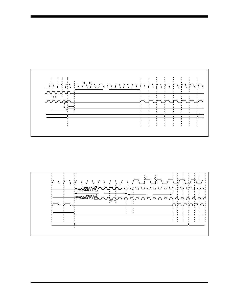
2.6.2
OSCILLATOR TRANSITIONS
The PIC18CXX2 devices contain circuitry to prevent
"glitches" when switching between oscillator sources.
Essentially, the circuitry waits for eight rising edges of
the clock source that the processor is switching to. This
ensures that the new clock source is stable and that its
pulse width will not be less than the shortest pulse
width of the two clock sources.
A timing diagram indicating the transition from the
main oscillator to the Timer1 oscillator is shown in
Figure 2-8. The Timer1 oscillator is assumed to be
running all the time. After the SCS bit is set, the pro-
cessor is frozen at the next occurring Q1 cycle. After
eight synchronization cycles are counted from the
Timer1 oscillator, operation resumes. No additional
delays are required after the synchronization cycles.
FIGURE 2-8:
TIMING DIAGRAM FOR TRANSITION FROM OSC1 TO TIMER1 OSCILLATOR
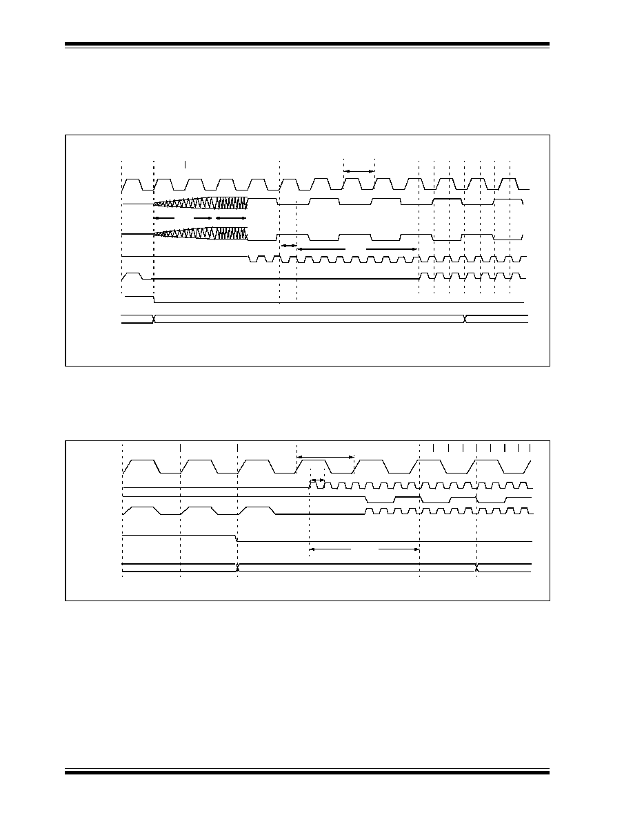
The sequence of events that takes place when switch-
ing from the Timer1 oscillator to the main oscillator will
depend on the mode of the main oscillator. In addition
to eight clock cycles of the main oscillator, additional
delays may take place.
If the main oscillator is configured for an external crys-
tal (HS, XT, LP), then the transition will take place after
an oscillator startup time (T
OST
) has occurred. A timing
diagram indicating the transition from the Timer1 oscil-
lator to the main oscillator for HS, XT and LP modes is
shown in Figure 2-9.
FIGURE 2-9:
TIMING FOR TRANSITION BETWEEN TIMER1 AND OSC1 (HS,XT,LP)
Q3
Q2
Q1
Q4
Q3
Q2
OSC1
Internal
SCS
(OSCCON<0>)
Program
PC + 2
PC
Note 1: Delay on internal system clock is eight oscillator cycles for synchronization.
Q1
T1OSI
Q4
Q1
PC + 4
Q1
Tscs
Clock
Counter
System
Q2
Q3
Q4
Q1
T
DLY
T
T
1
P
T
OSC
2
1
3
4
5
6
7
8
Q3
Q3
Q4
Q1
Q2
Q3
Q4
Q1
Q2
OSC1
Internal System
SCS
(OSCCON<0>)
Program Counter
PC
PC + 2
Note 1: T
OST
= 1024T
OSC
(drawing not to scale).
T1OSI
Clock
OSC2
T
OST
Q1
PC + 6
T
T
1
P
T
OSC
T
SCS
1
2
3
4
5
6
7
8
PIC18CXX2
DS39026B-page 20
Preliminary
©
7/99 Microchip Technology Inc.
If the main oscillator is configured for HS-PLL mode, an
oscillator startup time (T
OST
) plus an additional PLL
timeout (T
PLL
) will occur. The PLL timeout is typically 2
ms and allows the PLL to lock to the main oscillator fre-
quency. A timing diagram indicating the transition from
the Timer1 oscillator to the main oscillator for HS-PLL
mode is shown in Figure 2-10.
FIGURE 2-10: TIMING FOR TRANSITION BETWEEN TIMER1 AND OSC1 (HS WITH PLL)
If the main oscillator is configured in the RC, RCIO, EC
or ECIO modes, there is no oscillator startup timeout.
Operation will resume after eight cycles of the main
oscillator have been counted. A timing diagram indicat-
ing the transition from the Timer1 oscillator to the main
oscillator for RC, RCIO, EC and ECIO modes is shown
in Figure 2-11.
FIGURE 2-11: TIMING FOR TRANSITION BETWEEN TIMER1 AND OSC1 (RC, EC)
Q4
Q1
Q1
Q2 Q3
Q4
Q1 Q2
OSC1
Internal System
SCS
(OSCCON<0>)
Program Counter
PC
PC + 2
Note 1:
T
OST
= 1024T
OSC
(drawing not to scale).
T1OSI
Clock
T
OST
Q3
PC + 4
T
PLL
T
OSC
T
T
1
P
T
SCS
Q4
OSC2
PLL Clock
Input
1
2
3
4
5
6
7
8
Q3
Q4
Q1
Q1 Q2
Q3
Q4 Q1
Q2
Q3
OSC1
Internal System
SCS
(OSCCON<0>)
Program Counter
PC
PC + 2
Note 1: RC oscillator mode assumed.
PC + 4
T1OSI
Clock
OSC2
Q4
T
T
1
P
T
OSC
T
SCS
1
2
3
4
5
6
7
8
PIC18CXX2
©
7/99 Microchip Technology Inc.
Preliminary
DS39026B-page 21
2.7
Effects of Sleep Mode on the On-chip
Oscillator
When the device executes a SLEEP instruction, the on-
chip clocks and oscillator are turned off and the device
is held at the beginning of an instruction cycle (Q1
state). With the oscillator off, the OSC1 and OSC2 sig-
nals will stop oscillating. Since all the transistor switch-
ing currents have been removed, sleep mode achieves
the lowest current consumption of the device (only
leakage currents). Enabling any on-chip feature that
will operate during sleep will increase the current con-
sumed during sleep. The user can wake from SLEEP
through external reset, Watchdog Timer Reset or
through an interrupt.
TABLE 2-3:
OSC1 AND OSC2 PIN STATES IN SLEEP MODE
2.8
Power-up Delays
Power up delays are controlled by two timers, so that no
external reset circuitry is required for most applications.
The delays ensure that the device is kept in RESET
until the device power supply and clock are stable. For
additional information on RESET operation, see the
"Reset" section.
The first timer is the Power-up Timer (PWRT), which
optionally provides a fixed delay of 72 ms (nominal) on
power-up only (POR and BOR). The second timer is
the Oscillator Start-up Timer OST, intended to keep the
chip in RESET until the crystal oscillator is stable.
With the PLL enabled (HS/PLL oscillator mode), the
time-out sequence following a power-on reset is differ-
ent from other oscillator modes. The time-out sequence
is as follows: First the PWRT time-out is invoked after a
POR time delay has expired. Then the Oscillator Start-
up Timer (OST) is invoked. However, this is still not a
sufficient amount of time to allow the PLL to lock at high
frequencies. The PWRT timer is used to provide an
additional fixed 2ms (nominal) time-out to allow the PLL
ample time to lock to the incoming clock frequency.
OSC Mode
OSC1 Pin
OSC2 Pin
RC
Floating, external resistor should pull
high
At logic low
RCIO
Floating, external resistor should pull
high
Configured as Port A, bit 6
ECIO
Floating
Configured as Port A, bit 6
EC
Floating
At logic low
LP, XT, and HS
Feedback inverter disabled, at quies-
cent voltage level
Feedback inverter disabled, at quies-
cent voltage level
See Table 3-1, in the "Reset" section, for time-outs due to Sleep and MCLR reset.

PIC18CXX2
DS39026B-page 22
Preliminary
©
7/99 Microchip Technology Inc.
NOTES:
PIC18CXX2
©
7/99 Microchip Technology Inc.
Preliminary
DS39026B-page 23
3.0
RESET
The PIC18CXXX differentiates between various kinds
of reset:
a)
Power-on Reset (POR)
b)
MCLR reset during normal operation
c)
MCLR reset during SLEEP
d)
Watchdog Timer (WDT) Reset (during normal
operation)
e)
Programmable Brown-out Reset (BOR)
f)
Reset Instruction
g)
Stack Full reset
h)
Stack Underflow reset
Most registers are unaffected by a reset. Their status is
unknown on POR and unchanged by all other resets.
The other registers are forced to a "reset state" on
Power-on Reset, MCLR, WDT reset, Brown-out Reset,
MCLR reset during SLEEP and by the RESET instruc-
tion.
Most registers are not affected by a WDT wake-up,
since this is viewed as the resumption of normal oper-
ation. Status bits from the RCON register, RI, TO, PD,
POR and BOR, are set or cleared differently in different
reset situations, as indicated in Table 3-2. These bits
are used in software to determine the nature of the
reset. See Table 3-3 for a full description of the reset
states of all registers.
A simplified block diagram of the on-chip reset circuit is
shown in Figure 3-1.
The Enhanced MCU devices have a MCLR noise filter
in the MCLR reset path. The filter will detect and ignore
small pulses.
A WDT reset
does not drive MCLR pin low.
FIGURE 3-1:
SIMPLIFIED BLOCK DIAGRAM OF ON-CHIP RESET CIRCUIT
S
R
Q
External Reset
MCLR
V
DD
OSC1
WDT
Module
V
DD
rise
detect
OST/PWRT
On-chip
RC OSC
(1)
WDT
Time-out
Power-on Reset
OST
10-bit Ripple counter
PWRT
Chip_Reset
10-bit Ripple counter
Reset
Enable OST
(2)
Enable PWRT
SLEEP
Note 1: This is a separate oscillator from the RC oscillator of the CLKIN pin.
2: See Table 3-1 for time-out situations.
Brown-out
Reset
BOREN
RESET
Instruction
Stack
Pointer
Stack Full/Underflow Reset
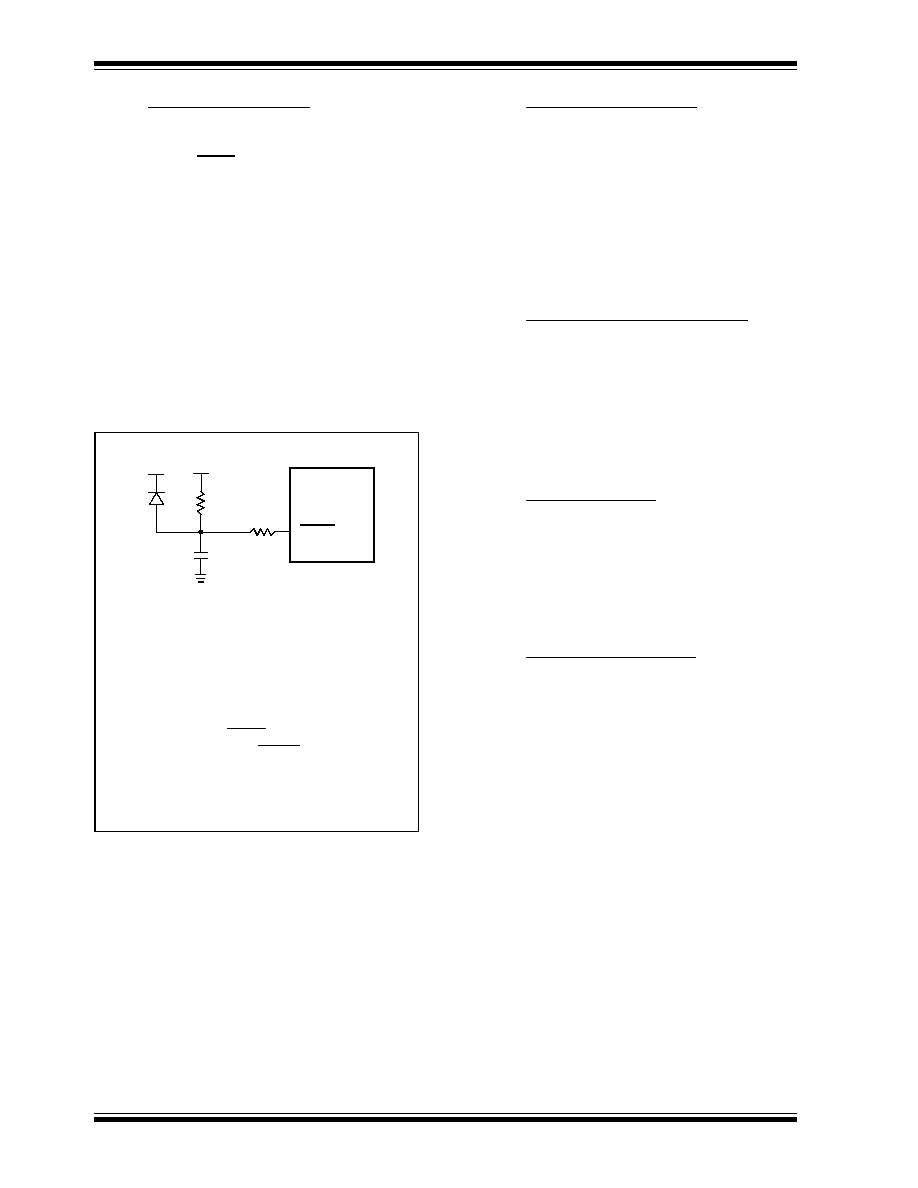
PIC18CXX2
DS39026B-page 24
Preliminary
©
7/99 Microchip Technology Inc.
3.1
Power-On Reset (POR)
A Power-on Reset pulse is generated on-chip when
V
DD
rise is detected. To take advantage of the POR cir-
cuitry, just tie the MCLR pin directly (or through a resis-
tor) to V
DD
. This will eliminate external RC components
usually needed to create a Power-on Reset delay. A
maximum rise time for V
DD
is specified (parameter
D004). For a slow rise time, see Figure 3-2.
When the device starts normal operation (exits the
reset condition), device operating parameters (voltage,
frequency, temperature,...) must be met to ensure oper-
ation. If these conditions are not met, the device must
be held in reset until the operating conditions are met.
Brown-out Reset may be used to meet the voltage
start-up condition.
FIGURE 3-2:
EXTERNAL POWER-ON
RESET CIRCUIT (FOR SLOW
V
DD
POWER-UP)
3.2
Power-up Timer (PWRT)
The Power-up Timer provides a fixed nominal time-out
(parameter #33) only on power-up from the POR. The
Power-up Timer operates on an internal RC oscillator.
The chip is kept in reset as long as the PWRT is active.
The PWRT's time delay allows V
DD
to rise to an accept-
able level. A configuration bit is provided to enable/dis-
able the PWRT.
The power-up time delay will vary from chip-to-chip due
to V
DD
, temperature and process variation. See DC
parameter #33 for details.
3.3
Oscillator Start-up Timer (OST)
The Oscillator Start-up Timer (OST) provides 1024
oscillator cycle (from OSC1 input) delay after the
PWRT delay is over (parameter #32). This ensures that
the crystal oscillator or resonator has started and stabi-
lized.
The OST time-out is invoked only for XT, LP and HS
modes and only on Power-on Reset or wake-up from
SLEEP.
3.4
PLL Lock Timeout
With the PLL enabled, the timeout sequence following
a power-on reset is different from other oscillator
modes. A portion of the Power-up Timer is used to pro-
vide a fixed timeout that is sufficient for the PLL to lock
to the main oscillator frequency. This PLL lock timeout
(T
PLL
) is typically 2 ms and follows the oscillator startup
timeout (OST).
3.5
Brown-Out Reset (BOR)
A configuration bit, BOREN, can disable (if clear/pro-
grammed) or enable (if set) the Brown-out Reset cir-
cuitry. If V
DD
falls below parameter D005 for greater
than parameter #35, the brown-out situation will reset
the chip. A reset may not occur if V
DD
falls below
parameter D005 for less than parameter #35. The chip
will remain in Brown-out Reset until V
DD
rises above
BV
DD
. The Power-up Timer will then be invoked and will
keep the chip in RESET an additional time delay
(parameter #33). If V
DD
drops below BV
DD
while the
Power-up Timer is running, the chip will go back into a
Brown-out Reset and the Power-up Timer will be initial-
ized. Once V
DD
rises above BV
DD
, the Power-up Timer
will execute the additional time delay.
Note 1: External Power-on Reset circuit is required
only if the V
DD
power-up slope is too slow.
The diode D helps discharge the capacitor
quickly when V
DD
powers down.
2: R < 40 k
is recommended to make sure
that the voltage drop across R does not
violate the device's electrical specification.
3: R1 = 100
to 1 k
will limit any current
flowing into MCLR from external capacitor
C in the event of MCLR/V
PP
pin break-
down due to Electrostatic Discharge
(ESD) or Electrical Overstress (EOS).
C
R1
R
D
V
DD
MCLR
PIC18CXXX
PIC18CXX2
©
7/99 Microchip Technology Inc.
Preliminary
DS39026B-page 25
3.6
Time-out Sequence
On power-up, the time-out sequence is as follows: First,
PWRT time-out is invoked after the POR time delay has
expired. Then, OST is activated. The total time-out will
vary based on oscillator configuration and the status of
the PWRT. For example, in RC mode with the PWRT
disabled, there will be no time-out at all. Figure 3-3,
Figure 3-4, Figure 3-5, Figure 3-6 and Figure 3-7
depict time-out sequences on power-up.
Since the time-outs occur from the POR pulse, if MCLR
is kept low long enough, the time-outs will expire.
Bringing MCLR high will begin execution immediately
(Figure 3-5). This is useful for testing purposes or to
synchronize more than one PIC18CXXX device operat-
ing in parallel.
Table 3-2 shows the reset conditions for some Special
Function Registers, while Table 3-3 shows the reset
conditions for all the registers.
TABLE 3-1:
TIME-OUT IN VARIOUS SITUATIONS
Register 3-1:
RCON Register Bits and Positions
TABLE 3-2:
STATUS BITS, THEIR SIGNIFICANCE AND THE INITIALIZATION CONDITION FOR
RCON REGISTER
Oscillator
Configuration
Power-up
(2)
Brown-out
(2)
Wake-up from
SLEEP or
Oscillator Switch
PWRTE = 0
PWRTE = 1
HS with PLL enabled
(1)
72 ms + 1024Tosc + 2ms 1024Tosc + 2 ms 72 ms + 1024Tosc + 2ms 1024Tosc + 2 ms
HS, XT, LP
72 ms + 1024Tosc
1024Tosc
72 ms + 1024Tosc
1024Tosc
EC
72 ms
--
72 ms
--
External RC
72 ms
--
72 ms
--
Note 1: 2 ms = Nominal time required for the 4x PLL to lock.
2: 72 ms is the nominal power-up timer delay
R/W-0
R/W-0
U-0
R/W-1
R/W-1
R/W-1
R/W-1
R/W-1
IPEN
LWRT
--
RI
TO
PD
POR
BOR
bit 7
bit 0
Condition
Program
Counter
RCON
Register
RI
TO
PD
POR
BOR
STKFUL
STKUNF
Power-on Reset
0000h
00-1 1100
1
1
1
0
0
u
u
MCLR Reset during normal
operation
0000h
00-u uuuu
u
u
u
u
u
u
u
Software Reset during normal
operation
0000h
0u-0 uuuu
0
u
u
u
u
u
u
Stack Full Reset during normal
operation
0000h
0u-u uu11
u
u
u
u
u
u
1
Stack Underflow Reset during
normal operation
0000h
0u-u uu11
u
u
u
u
u
1
u
MCLR Reset during SLEEP
0000h
00-u 10uu
u
1
0
u
u
u
u
WDT Reset
0000h
0u-u 01uu
1
0
1
u
u
u
u
WDT Wake-up
PC + 2
uu-u 00uu
u
0
0
u
u
u
u
Brown-out Reset
0000h
0u-1 11u0
1
1
1
1
0
u
u
Interrupt wake-up from SLEEP
PC + 2
(
1
)
uu-u 00uu
u
1
0
u
u
u
u
Legend: u = unchanged, x = unknown, -- = unimplemented bit read as '0'.
Note 1: When the wake-up is due to an interrupt and the GIEH or GIEL bits are set, the PC is loaded with the
interrupt vector (
0x000008h or 0x000018h
).
PIC18CXX2
DS39026B-page 26
Preliminary
©
7/99 Microchip Technology Inc.
TABLE 3-3:
INITIALIZATION CONDITIONS FOR ALL REGISTERS
Register
Applicable Devices
Power-on Reset,
Brown-out Reset
MCLR Resets
WDT Reset
Reset Instruction
Stack Resets
Wake-up via WDT
or Interrupt
TOSU
242
442
252
452
---0 0000
---0 0000
---0 uuuu
(3)
TOSH
242
442
252
452
0000 0000
0000 0000
uuuu uuuu
(3)
TOSL
242
442
252
452
0000 0000
0000 0000
uuuu uuuu
(3)
STKPTR
242
442
252
452
00-0 0000
00-0 0000
uu-u uuuu
(3)
PCLATU
242
442
252
452
---0 0000
---0 0000
---u uuuu
PCLATH
242
442
252
452
0000 0000
0000 0000
uuuu uuuu
PCL
242
442
252
452
0000 0000
0000 0000
PC + 2
(2)
TBLPTRU
242
442
252
452
--00 0000
--00 0000
--uu uuuu
TBLPTRH
242
442
252
452
0000 0000
0000 0000
uuuu uuuu
TBLPTRL
242
442
252
452
0000 0000
0000 0000
uuuu uuuu
TABLAT
242
442
252
452
0000 0000
0000 0000
uuuu uuuu
PRODH
242
442
252
452
xxxx xxxx
uuuu uuuu
uuuu uuuu
PRODL
242
442
252
452
xxxx xxxx
uuuu uuuu
uuuu uuuu
INTCON
242
442
252
452
0000 000x
0000 000u
uuuu uuuu
(1)
INTCON2
242
442
252
452
1111 -1-1
1111 -1-1
uuuu -u-u
(1)
INTCON3
242
442
252
452
11-0 0-00
11-0 0-00
uu-u u-uu
(1)
INDF0
242
442
252
452
N/A
N/A
N/A
POSTINC0
242
442
252
452
N/A
N/A
N/A
POSTDEC0 242
442
252
452
N/A
N/A
N/A
PREINC0
242
442
252
452
N/A
N/A
N/A
PLUSW0
242
442
252
452
N/A
N/A
N/A
FSR0H
242
442
252
452
---- 0000
---- 0000
---- uuuu
FSR0L
242
442
252
452
xxxx xxxx
uuuu uuuu
uuuu uuuu
WREG
242
442
252
452
xxxx xxxx
uuuu uuuu
uuuu uuuu
INDF1
242
442
252
452
N/A
N/A
N/A
POSTINC1
242
442
252
452
N/A
N/A
N/A
POSTDEC1 242
442
252
452
N/A
N/A
N/A
PREINC1
242
442
252
452
N/A
N/A
N/A
PLUSW1
242
442
252
452
N/A
N/A
N/A
Legend: u = unchanged, x = unknown,
-
= unimplemented bit, read as '0', q = value depends on condition
Note 1: One or more bits in the INTCONx or PIRx registers will be affected (to cause wake-up).
2: When the wake-up is due to an interrupt and the GIEL or GIEH bit is set, the PC is loaded with the interrupt
vector (
0008h or 0018h
).
3: When the wake-up is due to an interrupt and the GIEL or GIEH bit is set, the TOSU, TOSH and TOSL are
updated with the current value of the PC. The STKPTR is modified to point to the next location in the hard-
ware stack.
4: See Table 3-2 for reset value for specific condition.
5: Bit 6 of PORTA, LATA, and TRISA are enabled in ECIO and RCIO oscillator modes only. In all other
oscillator modes, they are disabled and read '0'.
6: The long write enable is only reset on a POR or MCLR reset.
7: Bit 6 of PORTA, LATA and TRISA are not available on all devices. When unimplemented, they are read '0'.
PIC18CXX2
©
7/99 Microchip Technology Inc.
Preliminary
DS39026B-page 27
FSR1H
242
442
252
452
---- 0000
---- 0000
---- uuuu
FSR1L
242
442
252
452
xxxx xxxx
uuuu uuuu
uuuu uuuu
BSR
242
442
252
452
---- 0000
---- 0000
---- uuuu
INDF2
242
442
252
452
N/A
N/A
N/A
POSTINC2
242
442
252
452
N/A
N/A
N/A
POSTDEC2 242
442
252
452
N/A
N/A
N/A
PREINC2
242
442
252
452
N/A
N/A
N/A
PLUSW2
242
442
252
452
N/A
N/A
N/A
FSR2H
242
442
252
452
---- 0000
---- 0000
---- uuuu
FSR2L
242
442
252
452
xxxx xxxx
uuuu uuuu
uuuu uuuu
STATUS
242
442
252
452
---x xxxx
---u uuuu
---u uuuu
TMR0H
242
442
252
452
xxxx xxxx
uuuu uuuu
uuuu uuuu
TMR0L
242
442
252
452
xxxx xxxx
uuuu uuuu
uuuu uuuu
T0CON
242
442
252
452
1111 1111
1111 1111
uuuu uuuu
OSCCON
242
442
252
452
---- ---0
---- ---0
---- ---u
LVDCON
242
442
252
452
--00 0101
--00 0101
--uu uuuu
WDTCON
242
442
252
452
---- ---0
---- ---0
---- ---u
RCON
(4, 6)
242
442
252
452
00-1 11q0
00-1 qquu
uu-u qquu
TMR1H
242
442
252
452
xxxx xxxx
uuuu uuuu
uuuu uuuu
TMR1L
242
442
252
452
xxxx xxxx
uuuu uuuu
uuuu uuuu
T1CON
242
442
252
452
0-00 0000
u-uu uuuu
u-uu uuuu
TMR2
242
442
252
452
xxxx xxxx
uuuu uuuu
uuuu uuuu
PR2
242
442
252
452
1111 1111
1111 1111
1111 1111
T2CON
242
442
252
452
-000 0000
-000 0000
-uuu uuuu
SSPBUF
242
442
252
452
xxxx xxxx
uuuu uuuu
uuuu uuuu
SSPADD
242
442
252
452
0000 0000
0000 0000
uuuu uuuu
SSPSTAT
242
442
252
452
0000 0000
0000 0000
uuuu uuuu
SSPCON1
242
442
252
452
0000 0000
0000 0000
uuuu uuuu
SSPCON2
242
442
252
452
0000 0000
0000 0000
uuuu uuuu
TABLE 3-3:
INITIALIZATION CONDITIONS FOR ALL REGISTERS (Cont.'d)
Register
Applicable Devices
Power-on Reset,
Brown-out Reset
MCLR Resets
WDT Reset
Reset Instruction
Stack Resets
Wake-up via WDT
or Interrupt
Legend: u = unchanged, x = unknown,
-
= unimplemented bit, read as '0', q = value depends on condition
Note 1: One or more bits in the INTCONx or PIRx registers will be affected (to cause wake-up).
2: When the wake-up is due to an interrupt and the GIEL or GIEH bit is set, the PC is loaded with the interrupt
vector (
0008h or 0018h
).
3: When the wake-up is due to an interrupt and the GIEL or GIEH bit is set, the TOSU, TOSH and TOSL are
updated with the current value of the PC. The STKPTR is modified to point to the next location in the hard-
ware stack.
4: See Table 3-2 for reset value for specific condition.
5: Bit 6 of PORTA, LATA, and TRISA are enabled in ECIO and RCIO oscillator modes only. In all other
oscillator modes, they are disabled and read '0'.
6: The long write enable is only reset on a POR or MCLR reset.
7: Bit 6 of PORTA, LATA and TRISA are not available on all devices. When unimplemented, they are read '0'.
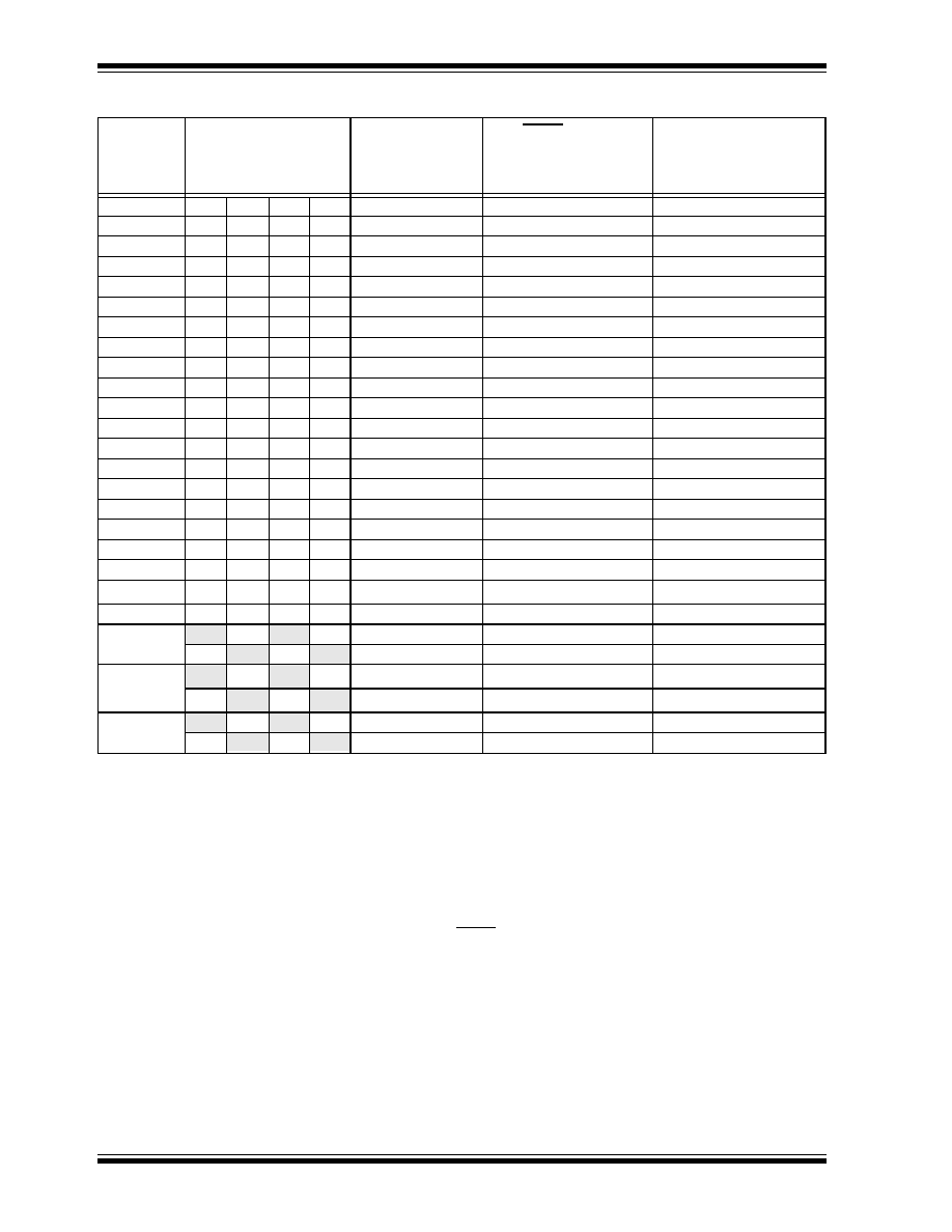
PIC18CXX2
DS39026B-page 28
Preliminary
©
7/99 Microchip Technology Inc.
ADRESH
242
442
252
452
xxxx xxxx
uuuu uuuu
uuuu uuuu
ADRESL
242
442
252
452
xxxx xxxx
uuuu uuuu
uuuu uuuu
ADCON0
242
442
252
452
0000 0000
0000 0000
uuuu uuuu
ADCON1
242
442
252
452
--0- 0000
--0- 0000
--u- uuuu
CCPR1H
242
442
252
452
xxxx xxxx
uuuu uuuu
uuuu uuuu
CCPR1L
242
442
252
452
xxxx xxxx
uuuu uuuu
uuuu uuuu
CCP1CON
242
442
252
452
--00 0000
--00 0000
--uu uuuu
CCPR2H
242
442
252
452
xxxx xxxx
uuuu uuuu
uuuu uuuu
CCPR2L
242
442
252
452
xxxx xxxx
uuuu uuuu
uuuu uuuu
CCP2CON
242
442
252
452
--00 0000
--00 0000
--uu uuuu
TMR3H
242
442
252
452
xxxx xxxx
uuuu uuuu
uuuu uuuu
TMR3L
242
442
252
452
xxxx xxxx
uuuu uuuu
uuuu uuuu
T3CON
242
442
252
452
0000 0000
uuuu uuuu
uuuu uuuu
SPBRG
242
442
252
452
xxxx xxxx
uuuu uuuu
uuuu uuuu
RCREG
242
442
252
452
xxxx xxxx
uuuu uuuu
uuuu uuuu
TXREG
242
442
252
452
xxxx xxxx
uuuu uuuu
uuuu uuuu
TXSTA
242
442
252
452
0000 -01x
0000 -01u
uuuu -uuu
RCSTA
242
442
252
452
0000 000x
0000 000u
uuuu uuuu
IPR2
242
442
252
452
---- 1111
---- 1111
---- uuuu
PIR2
242
442
252
452
---- 0000
---- 0000
---- uuuu
(1)
PIE2
242
442
252
452
---- 0000
---- 0000
---- uuuu
IPR1
242
442
252
452
1111 1111
1111 1111
uuuu uuuu
242
442
252
452
-111 1111
-111 1111
-uuu uuuu
PIR1
242
442
252
452
0000 0000
0000 0000
uuuu uuuu
(1)
242
442
252
452
-000 0000
-000 0000
-uuu uuuu
(1)
PIE1
242
442
252
452
0000 0000
0000 0000
uuuu uuuu
242
442
252
452
-000 0000
-000 0000
-uuu uuuu
TABLE 3-3:
INITIALIZATION CONDITIONS FOR ALL REGISTERS (Cont.'d)
Register
Applicable Devices
Power-on Reset,
Brown-out Reset
MCLR Resets
WDT Reset
Reset Instruction
Stack Resets
Wake-up via WDT
or Interrupt
Legend: u = unchanged, x = unknown,
-
= unimplemented bit, read as '0', q = value depends on condition
Note 1: One or more bits in the INTCONx or PIRx registers will be affected (to cause wake-up).
2: When the wake-up is due to an interrupt and the GIEL or GIEH bit is set, the PC is loaded with the interrupt
vector (
0008h or 0018h
).
3: When the wake-up is due to an interrupt and the GIEL or GIEH bit is set, the TOSU, TOSH and TOSL are
updated with the current value of the PC. The STKPTR is modified to point to the next location in the hard-
ware stack.
4: See Table 3-2 for reset value for specific condition.
5: Bit 6 of PORTA, LATA, and TRISA are enabled in ECIO and RCIO oscillator modes only. In all other
oscillator modes, they are disabled and read '0'.
6: The long write enable is only reset on a POR or MCLR reset.
7: Bit 6 of PORTA, LATA and TRISA are not available on all devices. When unimplemented, they are read '0'.
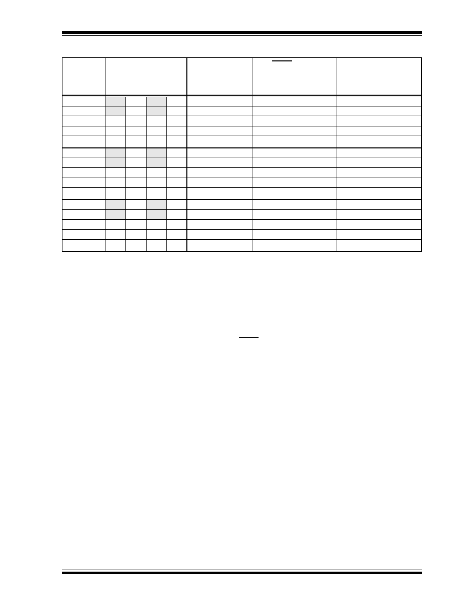
PIC18CXX2
©
7/99 Microchip Technology Inc.
Preliminary
DS39026B-page 29
TRISE
242
442
252
452
0000 -111
0000 -111
uuuu -uuu
TRISD
242
442
252
452
1111 1111
1111 1111
uuuu uuuu
TRISC
242
442
252
452
1111 1111
1111 1111
uuuu uuuu
TRISB
242
442
252
452
1111 1111
1111 1111
uuuu uuuu
TRISA
(5, 7)
242
442
252
452
-111 1111
(5)
-111 1111
(5)
-uuu uuuu
(5)
LATE
242
442
252
452
---- -xxx
---- -uuu
---- -uuu
LATD
242
442
252
452
xxxx xxxx
uuuu uuuu
uuuu uuuu
LATC
242
442
252
452
xxxx xxxx
uuuu uuuu
uuuu uuuu
LATB
242
442
252
452
xxxx xxxx
uuuu uuuu
uuuu uuuu
LATA
(5, 7)
242
442
252
452
-xxx xxxx
(5)
-uuu uuuu
(5)
-uuu uuuu
(5)
PORTE
242
442
252
452
---- -000
---- -000
---- -uuu
PORTD
242
442
252
452
xxxx xxxx
uuuu uuuu
uuuu uuuu
PORTC
242
442
252
452
xxxx xxxx
uuuu uuuu
uuuu uuuu
PORTB
242
442
252
452
xxxx xxxx
uuuu uuuu
uuuu uuuu
PORTA
(5, 7)
242
442
252
452
-x0x 0000
(5)
-u0u 0000
(5)
-uuu uuuu
(5)
TABLE 3-3:
INITIALIZATION CONDITIONS FOR ALL REGISTERS (Cont.'d)
Register
Applicable Devices
Power-on Reset,
Brown-out Reset
MCLR Resets
WDT Reset
Reset Instruction
Stack Resets
Wake-up via WDT
or Interrupt
Legend: u = unchanged, x = unknown,
-
= unimplemented bit, read as '0', q = value depends on condition
Note 1: One or more bits in the INTCONx or PIRx registers will be affected (to cause wake-up).
2: When the wake-up is due to an interrupt and the GIEL or GIEH bit is set, the PC is loaded with the interrupt
vector (
0008h or 0018h
).
3: When the wake-up is due to an interrupt and the GIEL or GIEH bit is set, the TOSU, TOSH and TOSL are
updated with the current value of the PC. The STKPTR is modified to point to the next location in the hard-
ware stack.
4: See Table 3-2 for reset value for specific condition.
5: Bit 6 of PORTA, LATA, and TRISA are enabled in ECIO and RCIO oscillator modes only. In all other
oscillator modes, they are disabled and read '0'.
6: The long write enable is only reset on a POR or MCLR reset.
7: Bit 6 of PORTA, LATA and TRISA are not available on all devices. When unimplemented, they are read '0'.
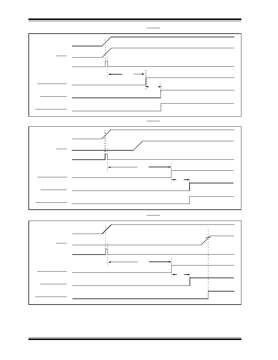
PIC18CXX2
DS39026B-page 30
Preliminary
©
7/99 Microchip Technology Inc.
FIGURE 3-3:
TIME-OUT SEQUENCE ON POWER-UP (MCLR TIED TO V
DD
)
FIGURE 3-4:
TIME-OUT SEQUENCE ON POWER-UP (MCLR NOT TIED TO V
DD
): CASE 1
FIGURE 3-5:
TIME-OUT SEQUENCE ON POWER-UP (MCLR NOT TIED TO V
DD
): CASE 2
T
PWRT
T
OST
V
DD
MCLR
INTERNAL POR
PWRT TIME-OUT
OST TIME-OUT
INTERNAL RESET
T
PWRT
T
OST
V
DD
MCLR
INTERNAL POR
PWRT TIME-OUT
OST TIME-OUT
INTERNAL RESET
V
DD
MCLR
INTERNAL POR
PWRT TIME-OUT
OST TIME-OUT
INTERNAL RESET
T
PWRT
T
OST
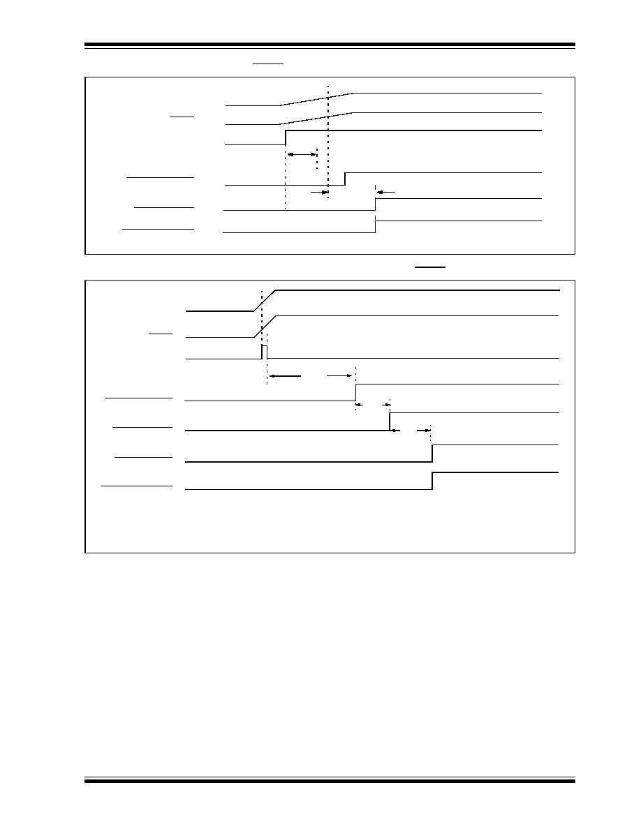
PIC18CXX2
©
7/99 Microchip Technology Inc.
Preliminary
DS39026B-page 31
FIGURE 3-6:
SLOW RISE TIME (MCLR TIED TO V
DD
)
FIGURE 3-7:
TIME-OUT SEQUENCE ON POR W/ PLL ENABLED (MCLR TIED TO V
DD
)
V
DD
MCLR
INTERNAL POR
PWRT TIME-OUT
OST TIME-OUT
INTERNAL RESET
0V
1V
5V
T
PWRT
T
OST
T
PWRT
T
OST
V
DD
MCLR
IINTERNAL POR
PWRT TIME-OUT
OST TIME-OUT
INTERNAL RESET
PLL TIME-OUT
T
PLL
T
OST
= 1024 clock cycles.
T
PLL
2 ms max. First three stages of the PWRT timer.

PIC18CXX2
DS39026B-page 32
Preliminary
©
7/99 Microchip Technology Inc.
NOTES:

PIC18CXX2
©
7/99 Microchip Technology Inc.
Preliminary
DS39026B-page 33
4.0
MEMORY ORGANIZATION
There are two memory blocks in Enhanced MCU
devices. These memory blocks are:
∑ Program Memory
∑ Data Memory
Each block has its own bus so that concurrent access
can occur.
4.1
Program Memory Organization
A 21-bit program counter is capable of addressing the
2-Mbyte program memory space. Accessing a location
between the physically implemented memory and the
2-Mbyte address will cause a read of all '0's (a
NOP
instruction).
PIC18C252 and PIC18C452 have 32-KBytes of
EPROM, while PIC18C242 and PIC18C442 have
16-KBytes of EPROM. This means that PIC18CX52
devices can store up to 16K of single word instruc-
tions, and PIC18CX42 devices can store up to 8K of
single word instructions.
The reset vector address is at 0000h and the interrupt
vector addresses are at 0008h and 0018h.
Figure 4-1 shows the Program Memory Map for
PIC18C242/442 devices and Figure 4-2 shows the
Program Memory Map for PIC18C252/452 devices.
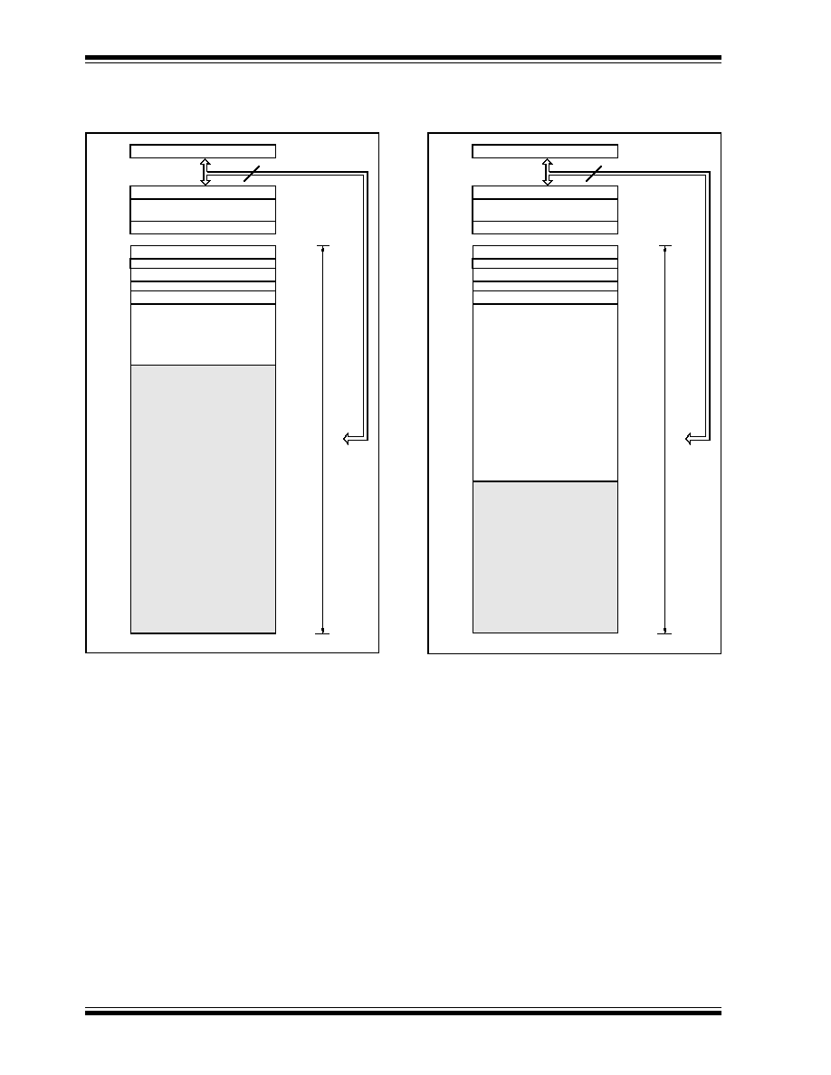
DS39026B-page 34
Preliminary
©
7/99 Microchip Technology Inc.
PIC18CXX2
FIGURE 4-1:
PROGRAM MEMORY MAP
AND STACK FOR PIC18C442/
242
FIGURE 4-2:
PROGRAM MEMORY MAP
AND STACK FOR PIC18C452/
252
PC<20:0>
Stack Level 1
∑
Stack Level 31
Reset Vector
Low Priority Interrupt Vector
∑
∑
CALL,BSUB,RETURN
RETFIE,RETLW
21
0000h
0018h
On-chip
Program Memory
High Priority Interrupt Vector
0008h
User Mem
o
r
y
Spac
e
1FFFFFh
4000h
3FFFh
Read '0'
200000h
PC<20:0>
Stack Level 1
∑
Stack Level 31
Reset Vector
Low Priority Interrupt Vector
∑
∑
CALL,BSUB,RETURN
RETFIE,RETLW
21
0000h
0018h
8000h
7FFFh
On-chip
Program Memory
High Priority Interrupt Vector
0008h
User Mem
o
r
y
Spac
e
Read '0'
1FFFFFh
200000h

PIC18CXX2
©
7/99 Microchip Technology Inc.
Preliminary
DS39026B-page 35
4.2
Return Address Stack
The return address stack allows any combination of up
to 31 program calls and interrupts to occur. The PC
(Program Counter) is pushed onto the stack when a
CALL
or
RCALL
instruction is executed or an interrupt is
acknowledged. The PC value is pulled off the stack on
a
RETURN, RETLW
or a
RETFIE
instruction.
PCLATU
and
PCLATH
are not affected by any of the return
instructions.
The stack operates as a 31 word by 21-bit RAM and a
5-bit stack pointer, with the stack pointer initialized to
00000b after all resets. There is no RAM associated
with stack pointer 00000b. This is only a reset value.
During a
CALL
type instruction causing a push onto the
stack, the stack pointer is first incremented and the
RAM location pointed to by the stack pointer is written
with the contents of the PC. During a
RETURN
type
instruction causing a pop from the stack, the contents
of the RAM location pointed to by the STKPTR is trans-
ferred to the PC and then the stack pointer is decre-
mented.
The stack space is not part of either program or data
space. The stack pointer is readable and writable, and
the address on the top of the stack is readable and writ-
able through SFR registers. Data can also be pushed
to or popped from the stack using the top-of-stack
SFRs. Status bits indicate if the stack pointer is at or
beyond the 31 levels provided.
4.2.1
TOP-OF-STACK ACCESS
The top of the stack is readable and writable. Three
register locations, TOSU, TOSH and TOSL hold the
contents of the stack location pointed to by the
STKPTR register. This allows users to implement a
software stack if necessary. After a
CALL, RCALL
or
interrupt, the software can read the pushed value by
reading the TOSU, TOSH and TOSL registers. These
values can be placed on a user defined software stack.
At return time, the software can replace the TOSU,
TOSH and TOSL and do a return.
The user must disable the global interrupt enable bits
during this time to prevent inadvertent stack operations.
4.2.2
RETURN STACK POINTER (STKPTR)
The STKPTR register contains the stack pointer value,
the STKFUL (stack full) status bit, and the STKUNF
(stack underflow) status bits. Register 4-1 shows the
STKPTR register. The value of the stack pointer can be
0 through 31. The stack pointer increments when val-
ues are pushed onto the stack and decrements when
values are popped off the stack. At reset, the stack
pointer value will be 0. The user may read and write the
stack pointer value. This feature can be used by a Real
Time Operating System for return stack maintenance.
After the PC is pushed onto the stack 31 times (without
popping any values off the stack), the STKFUL bit is
set. The STKFUL bit can only be cleared in software or
by a POR.
The action that takes place when the stack becomes
full depends on the state of the STVREN (stack over-
flow reset enable) configuration bit. Refer to Section 18
for a description of the device configuration bits. If
STVREN is set (default) the 31st push will push the (PC
+ 2) value onto the stack, set the STKFUL bit, and reset
the device. The STKFUL bit will remain set and the
stack pointer will be set to 0.
If STVREN is cleared, the STKFUL bit will be set on the
31st push and the stack pointer will increment to 31.
The 32nd push will overwrite the 31st push (and so on),
while STKPTR remains at 31.
When the stack has been popped enough times to
unload the stack, the next pop will return a value of zero
to the PC and sets the STKUNF bit, while the stack
pointer remains at 0. The STKUNF bit will remain set
until cleared in software or a POR occurs.
Note:
Returning a value of zero to the PC on an
underflow has the effect of vectoring the
program to the reset vector, where the
stack conditions can be verified and appro-
priate actions can be taken.
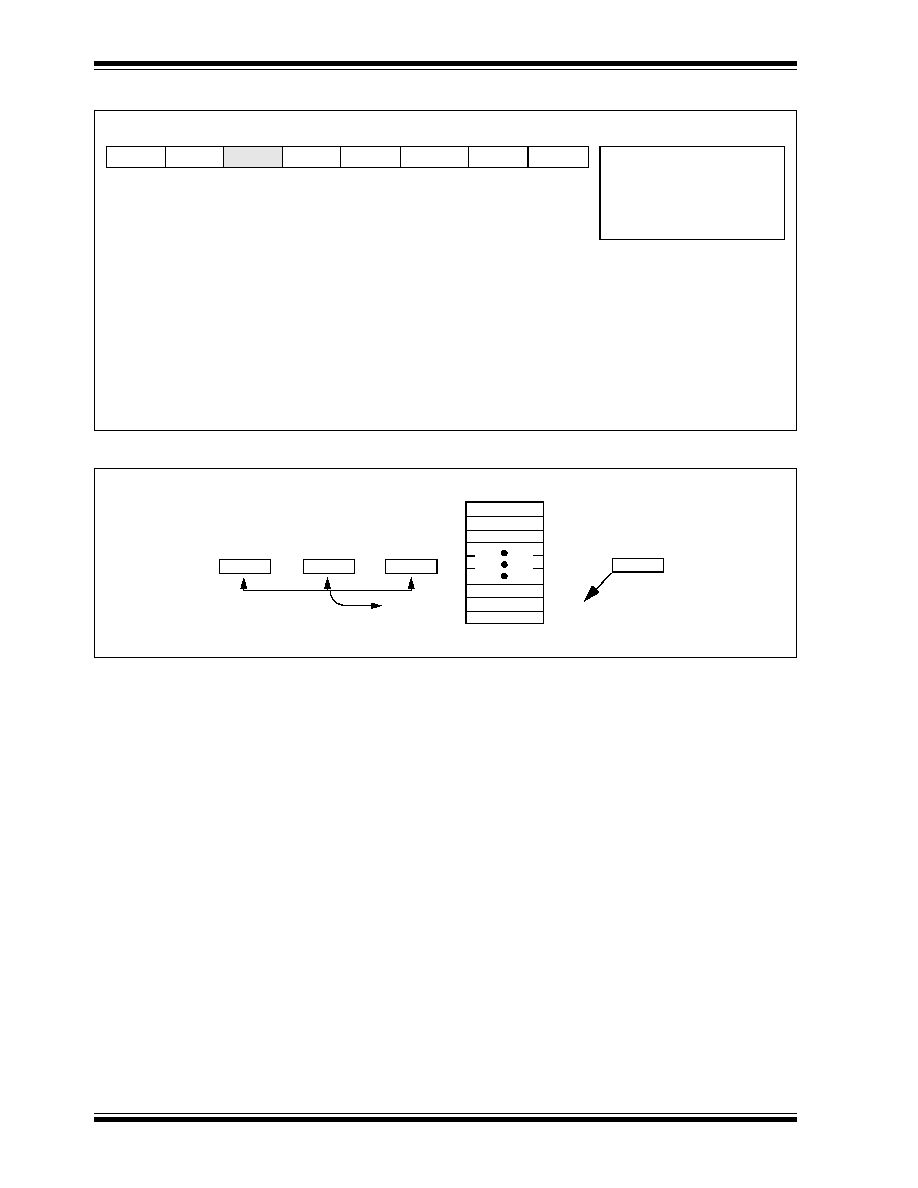
DS39026B-page 36
Preliminary
©
7/99 Microchip Technology Inc.
PIC18CXX2
Register 4-1:
STKPTR - Stack Pointer Register
FIGURE 4-3:
RETURN ADDRESS STACK AND ASSOCIATED REGISTERS
4.2.3
PUSH AND POP INSTRUCTIONS
Since the Top-of-Stack (TOS) is readable and writable,
the ability to push values onto the stack and pull values
off the stack without disturbing normal program execu-
tion is a desirable option. To push the current PC value
onto the stack, a
PUSH
instruction can be executed.
This will increment the stack pointer and load the cur-
rent PC value onto the stack. TOSU, TOSH and TOSL
can then be modified to place a return address on the
stack.
The ability to pull the TOS value off of the stack and
replace it with the value that was previously pushed
onto the stack, without disturbing normal execution, is
achieved by using the
POP
instruction. The
POP
instruc-
tion discards the current TOS by decrementing the
stack pointer. The previous value pushed onto the
stack then becomes the TOS value.
4.2.4
STACK FULL/UNDERFLOW RESETS
These resets are enabled by programming the
STVREN configuration bit. When the STVREN bit is
disabled, a full or underflow condition will set the appro-
priate STKFUL or STKUNF bit, but not cause a device
reset. When the STVREN bit is enabled, a full or under-
flow will set the appropriate STKFUL or STKUNF bit
and then cause a device reset. The STKFUL or
STKUNF bits are only cleared by the user software or
a POR reset.
R/C-0
R/C-0
U-0
R/W-0
R/W-0
R/W-0
R/W-0
R/W-0
STKFUL
STKUNF
-
SP4
SP3
SP2
SP1
SP0
R
= Readable bit
W = Writeable bit
C
= Clearable bit
U
= Unimplemented bit,
Read as `0'
- n = Value at POR reset
bit7
6
5
4
3
2
1
bit0
bit 7
(1)
: STKFUL: Stack Full Flag bit
1
= Stack became full or overflowed
0
= Stack has not become full or overflowed
bit 6
(1)
: STKUNF: Stack Underflow Flag bit
1
= Stack underflow occurred
0
= Stack underflow did not occur
bit 5:
Unimplemented: Read as '0'
bit 4-0:
SP4:SP0: Stack Pointer Location bits
Note 1: Bit 7 and Bit 6 can only be cleared in user software or by a POR.
00011
0x001A34
11111
11110
11101
00010
00001
00000
00010
Return Address Stack
Top of Stack
0x000D58
TOSL
TOSH
TOSU
0x34
0x1A
0x00
STKPTR<4:0>
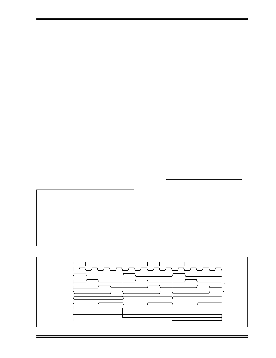
PIC18CXX2
©
7/99 Microchip Technology Inc.
Preliminary
DS39026B-page 37
4.3
Fast Register Stack
A "fast interrupt return" option is available for interrupts.
A Fast Register Stack is provided for the STATUS,
WREG and BSR registers and are only one in depth.
The stack is not readable or writable and is loaded with
the current value of the corresponding register when
the processor vectors for an interrupt. The values in the
registers are then loaded back into the working regis-
ters if the fast return instruction is used to return from
the interrupt.
A low or high priority interrupt source will push values
into the stack registers. If both low and high priority
interrupts are enabled, the stack registers cannot be
used reliably for low priority interrupts. If a high priority
interrupt occurs while servicing a low priority interrupt,
the stack register valves stored by the low priority inter-
rupt will be overwritten.
If high priority interrupts are not disabled during low pri-
ority interrupts, users must save the key registers in
software during a low priority interrupt.
If no interrupts are used, the fast register stack can be
used to restore the STATUS, WREG and BSR registers
at the end of a subroutine call. To use the fast register
stack for a subroutine call, a fast call instruction must be
executed.
Example 4-1 shows a source code example that uses
the fast register stack.
EXAMPLE 4-1:
FAST REGISTER STACK
CODE EXAMPLE
4.4
PCL, PCLATH and PCLATU
The program counter (PC) specifies the address of the
instruction to fetch for execution. The PC is 21-bits
wide. The low byte is called the PCL register. This reg-
ister is readable and writable. The high byte is called
the PCH register. This register contains the PC<15:8>
bits and is not directly readable or writable. Updates to
the PCH register may be performed through the
PCLATH register. The upper byte is called PCU. This
register contains the PC<20:16> bits and is not directly
readable or writable. Updates to the PCU register may
be performed through the PCLATU register.
The PC addresses bytes in the program memory. To
prevent the PC from becoming misaligned with word
instructions, the LSB of PCL is fixed to a value of '0'.
The PC increments by 2 to address sequential instruc-
tions in the program memory.
The
CALL, RCALL, GOTO
and program branch
instructions write to the program counter directly. For
these instructions, the contents of PCLATH and
PCLATU are not transferred to the program counter.
The contents of PCLATH and PCLATU will be trans-
ferred to the program counter by an operation that
writes PCL. Similarly, the upper two bytes of the pro-
gram counter will be transferred to PCLATH and
PCLATU by an operation that reads PCL. This is useful
for computed offsets to the PC. (See Section 4.8.1)
4.5
Clocking Scheme/Instruction Cycle
The clock input (from OSC1) is internally divided by
four to generate four non-overlapping quadrature
clocks namely Q1, Q2, Q3 and Q4. Internally, the pro-
gram counter (PC) is incremented every Q1, the
instruction is fetched from the program memory and
latched into the instruction register in Q4. The instruc-
tion is decoded and executed during the following Q1
through Q4. The clocks and instruction execution flow
is shown in Figure 4-4.
FIGURE 4-4:
CLOCK/INSTRUCTION CYCLE
CALL SUB1, FAST
;STATUS, WREG, BSR
;SAVED IN FAST REGISTER
;STACK
∑
∑
SUB1
∑
∑
∑
RETURN FAST
;RESTORE VALUES SAVED
;IN FAST REGISTER STACK
Q1
Q2
Q3
Q4
Q1
Q2
Q3
Q4
Q1
Q2
Q3
Q4
OSC1
Q1
Q2
Q3
Q4
PC
OSC2/CLKOUT
(RC mode)
PC
PC+2
PC+4
Fetch INST (PC)
Execute INST (PC-2)
Fetch INST (PC+2)
Execute INST (PC)
Fetch INST (PC+4)
Execute INST (PC+2)
Internal
phase
clock
DS39026B-page 38
Preliminary
©
7/99 Microchip Technology Inc.
PIC18CXX2
4.6
Instruction Flow/Pipelining
An "Instruction Cycle" consists of four Q cycles (Q1,
Q2, Q3 and Q4). The instruction fetch and execute are
pipelined such that fetch takes one instruction cycle
while decode and execute takes another instruction
cycle. However, due to the pipelining, each instruction
effectively executes in one cycle. If an instruction
causes the program counter to change (e.g.
GOTO
)
then two cycles are required to complete the instruction
(Example 4-2).
A fetch cycle begins with the program counter (PC)
incrementing in Q1.
In the execution cycle, the fetched instruction is latched
into the "Instruction Register" (IR) in cycle Q1. This
instruction is then decoded and executed during the
Q2, Q3, and Q4 cycles. Data memory is read during Q2
(operand read) and written during Q4 (destination
write).
EXAMPLE 4-2:
INSTRUCTION PIPELINE FLOW
4.7
Instructions in Program Memory
The program memory is addressed in bytes. Instruc-
tions are stored as two bytes or four bytes in program
memory. The least significant byte of an instruction
word is always stored in a program memory location
with an even address (LSB = '0'). Figure 4-5 shows an
example of how instruction words are stored in the pro-
gram memory. To maintain alignment with instruction
boundaries, the PC increments in steps of 2 and the
LSB will always read '0'. (See Section 4.4)
The
CALL
and
GOTO
instructions have an absolute
program memory address embedded into the instruc-
tion. Since instructions are always stored on word
boundaries, the data contained in the instruction is a
word address. The word address is written to
PC<20:1>, which accesses the desired byte address
in program memory. Instruction #2 in Figure 4-5
shows how the instruction "
GOTO 000006h
' is
encoded in the program memory. Program branch
instructions which encode a relative address offset
operate in the same manner. The offset value stored
in a branch instruction represents the number of sin-
gle word instructions that the PC will be offset by.
Section 19.0 provides further details of the instruction
set.
FIGURE 4-5:
INSTRUCTIONS IN PROGRAM MEMORY
All instructions are single cycle, except for any program branches. These take two cycles since the fetch
instruction is "flushed" from the pipeline while the new instruction is being fetched and then executed.
Tcy0
Tcy1
Tcy2
Tcy3
Tcy4
Tcy5
1. MOVLW 55h
Fetch 1
Execute 1
2. MOVWF PORTB
Fetch 2
Execute 2
3. BRA SUB_1
Fetch 3
Execute 3
4. BSF PORTA, BIT3 (Forced NOP)
Fetch 4
Flush
5. Instruction @ address SUB_1
Fetch SUB_1 Execute SUB_1
Word Address
LSB = 1
LSB = 0
Program Memory
Byte Locations
000000h
000002h
000004h
000006h
Instruction 1:
MOVLW
055h
0Fh
55h
000008h
Instruction 2:
GOTO
000006h
EFh
03h
00000Ah
F0h
00h
00000Ch
Instruction 3:
MOVFF
123h, 456h
C1h
23h
00000Eh
F4h
56h
000010h
000012h
000014h
PIC18CXX2
©
7/99 Microchip Technology Inc.
Preliminary
DS39026B-page 39
4.7.1
TWO-WORD INSTRUCTIONS
The PIC18CXX2 devices have 4 two-word instructions:
MOVFF, CALL, GOTO
and
LFSR
. The second word of
these instructions has the 4 MSB's set to 1's and is a
special kind of
NOP
instruction. The lower 12 bits of the
second word contain data to be used by the instruction.
If the first word of the instruction is executed, the data
in the second word is accessed. If the second word of
the instruction is executed by itself (first word was
skipped), it will execute as a
NOP
. This action is neces-
sary when the two word instruction is preceded by a
conditional instruction that changes the PC. A program
example that demonstrates this concept is shown in
Example 4-3. Refer to Section 19.0 for further details of
the instruction set.
EXAMPLE 4-3:
TWO-WORD INSTRUCTIONS
4.8
Lookup Tables
Look-up tables are implemented two ways. These are:
∑ Computed
GOTO
∑ Table Reads
4.8.1
COMPUTED GOTO
A computed
GOTO
is accomplished by adding an offset
to the program counter (
ADDWF PCL
).
A lookup table can be formed with an
ADDWF PCL
instruction and a group of
RETLW 0xnn
instructions.
WREG is loaded with an offset into the table before
executing a call to that table. The first instruction of the
called routine is the
ADDWF PCL
instruction. The next
instruction executed will be one of the
RETLW 0xnn
instructions that returns the value 0xnn to the calling
function.
The offset value (value in WREG) specifies the number
of bytes that the program counter should advance.
In this method, only one data byte may be stored in
each instruction location and room on the return
address stack is required.
4.8.2
TABLE READS/TABLE WRITES
A better method of storing data in program memory
allows 2 bytes of data to be stored in each instruction
location.
Lookup table data may be stored 2 bytes per program
word by using table reads and writes. The table pointer
(TBLPTR) specifies the byte address and the table
latch (TABLAT) contains the data that is read from or
written to program memory. Data is transferred to/from
program memory one byte at a time.
A description of the Table Read/Table Write operation
is shown in Section 5.0.
CASE 1:
Object code
Source Code
0110 0110 0000 0000
TSTFSZ
REG1
; is RAM location 0?
1100 0001 0010 0011
MOVFF
REG1, REG2 ; No, execute 2-word instruction
1111 0100 0101 0110
; 2nd operand holds address of REG2
0010 0100 0000 0000
ADDWF
REG3
; continue code
CASE 2:
Object code
Source Code
0110 0110 0000 0000
TSTFSZ
REG1
; is RAM location 0?
1100 0001 0010 0011
MOVFF
REG1, REG2 ; Yes
1111 0100 0101 0110
; 2nd operand becomes
NOP
0010 0100 0000 0000
ADDWF
REG3
; continue code

DS39026B-page 40
Preliminary
©
7/99 Microchip Technology Inc.
PIC18CXX2
4.9
Data Memory Organization
The data memory is implemented as static RAM. Each
register in the data memory has a 12-bit address,
allowing up to 4096 bytes of data memory. Figure 4-6
and Figure 4-7 show the data memory organization for
the PIC18CXX2 devices.
Banking is required to allow more than 256 bytes to be
accessed. The data memory map is divided into as
many as 16 banks that contain 256 bytes each. The
lower 4 bits of the Bank Select Register (BSR<3:0>)
select which bank will be accessed. The upper 4 bits
for the BSR are not implemented.
The data memory contains Special Function Registers
(SFR) and General Purpose Registers (GPR). The
SFRs are used for control and status of the controller
and peripheral functions, while GPRs are used for data
storage and scratch pad operations in the user's appli-
cation. The SFRs start at the last location of Bank 15
(OxFFF) and grow downwards. Any remaining space
beyond the SFRs in the Bank may be implemented as
GPRs. GPRs start at the first location of Bank 0 and
grow upwards. Any read of an unimplemented location
will read as '0's.
The entire data memory may be accessed directly or
indirectly. Direct addressing may require the use of the
BSR register. Indirect addressing requires the use of
the File Select Register (FSR). Each FSR holds a 12-
bit address value that can be used to access any loca-
tion in the Data Memory map without banking.
The instruction set and architecture allow operations
across all banks. This may be accomplished by indirect
addressing or by the use of the MOVFF instruction.
The MOVFF instruction is a two word/two cycle instruc-
tion that moves a value from one register to another.
To ensure that commonly used registers (SFRs and
select GPRs) can be accessed in a single cycle regard-
less of the current BSR values, an Access Bank is
implemented. A segment of Bank 0 and a segment of
Bank 15 comprise the Access RAM. Section 4.10 pro-
vides a detailed description of the Access RAM.
4.9.1
GENERAL PURPOSE REGISTER FILE
The register file can be accessed either directly or indi-
rectly. Indirect addressing operates through the File
Select Registers (FSR). The operation of indirect
addressing is shown in Section 4.12.
Enhanced MCU devices may have banked memory in
the GPR area. GPRs are not initialized by a Power-on
Reset and are unchanged on all other resets.
Data RAM is available for use as GPR registers by all
instructions. The top half of bank 15 (0xF80 to 0xFFF)
contains SFRs. All other banks of data memory contain
GPR registers starting with bank 0.
4.9.2
SPECIAL FUNCTION REGISTERS
The Special Function Registers (SFRs) are registers
used by the CPU and Peripheral Modules for controlling
the desired operation of the device. These registers are
implemented as static RAM. A list of these registers is
given in Table 4-1 and Table 4-2.
The SFRs can be classified into two sets; those asso-
ciated with the "core" function and those related to the
peripheral functions. Those registers related to the
"core" are described in this section, while those related
to the operation of the peripheral features are
described in the section of that peripheral feature.
The SFRs are typically distributed among the peripher-
als whose functions they control.
The unused SFR locations will be unimplemented and
read as '0's. See Table 4-1 for addresses for the SFRs.
PIC18CXX2
©
7/99 Microchip Technology Inc.
Preliminary
DS39026B-page 41
FIGURE 4-6:
DATA MEMORY MAP FOR PIC18C242/442
Bank 0
Bank 1
Bank 14
Bank 15
Data Memory Map
BSR<3:0>
= 0000b
= 0001b
= 1111b
080h
07Fh
F80h
FFFh
00h
7Fh
80h
FFh
Access Bank
When a = 0,
the BSR is ignored and the
Access Bank is used.
The first 128 bytes are
General Purpose RAM
(from Bank 0).
The second 128 bytes are
Special Function Registers
(from Bank 15).
When a = 1,
the BSR is used to specify
the RAM location that the
instruction uses.
F7Fh
F00h
EFFh
1FFh
100h
0FFh
000h
Access RAM
FFh
00h
FFh
00h
FFh
00h
GPR
GPR
SFR
Unused
Access RAM high
Access RAM low
Bank 2
to
200h
Unused
Read '00h'
= 1110b
= 0010b
(SFR's)
DS39026B-page 42
Preliminary
©
7/99 Microchip Technology Inc.
PIC18CXX2
FIGURE 4-7:
DATA MEMORY MAP FOR PIC18C252/452
Bank 0
Bank 1
Bank 14
Bank 15
Data Memory Map
BSR<3:0>
= 0000b
= 0001b
= 1110b
= 1111b
080h
07Fh
F80h
FFFh
00h
7Fh
80h
FFh
Access Bank
When a = 0,
the BSR is ignored and the
Access Bank is used.
The first 128 bytes are
General Purpose RAM
(from Bank 0).
The second 128 bytes are
Special Function Registers
(from Bank 15).
When a = 1,
the BSR is used to specify
the RAM location that the
instruction uses.
Bank 4
Bank 3
Bank 2
F7Fh
F00h
EFFh
3FFh
300h
2FFh
200h
1FFh
100h
0FFh
000h
= 0110b
= 0101b
= 0011b
= 0010b
Access RAM
FFh
00h
FFh
00h
FFh
00h
FFh
00h
FFh
00h
FFh
00h
GPR
GPR
GPR
GPR
SFR
Unused
Access RAM high
Access RAM low
Bank 5
GPR
GPR
Bank 6
to
4FFh
400h
5FFh
500h
600h
Unused
Read '00h'
= 0100b
(SFR's)

PIC18CXX2
©
7/99 Microchip Technology Inc.
Preliminary
DS39026B-page 43
TABLE 4-1:
SPECIAL FUNCTION REGISTER MAP
FFFh
TOSU
FDFh
INDF2
(3)
FBFh
CCPR1H
F9Fh
IPR1
FFEh
TOSH
FDEh
POSTINC2
(3)
FBEh
CCPR1L
F9Eh
PIR1
FFDh
TOSL
FDDh
POSTDEC2
(3)
FBDh
CCP1CON
F9Dh
PIE1
FFCh
STKPTR
FDCh
PREINC2
(3)
FBCh
CCPR2H
F9Ch
--
FFBh
PCLATU
FDBh
PLUSW2
(3)
FBBh
CCPR2L
F9Bh
--
FFAh
PCLATH
FDAh
FSR2H
FBAh
CCP2CON
F9Ah
--
FF9h
PCL
FD9h
FSR2L
FB9h
--
F99h
--
FF8h
TBLPTRU
FD8h
STATUS
FB8h
--
F98h
--
FF7h
TBLPTRH
FD7h
TMR0H
FB7h
--
F97h
--
FF6h
TBLPTRL
FD6h
TMR0L
FB6h
--
F96h
TRISE
(2)
FF5h
TABLAT
FD5h
T0CON
FB5h
--
F95h
TRISD
(2)
FF4h
PRODH
FD4h
--
FB4h
--
F94h
TRISC
FF3h
PRODL
FD3h
OSCCON
FB3h
TMR3H
F93h
TRISB
FF2h
INTCON
FD2h
LVDCON
FB2h
TMR3L
F92h
TRISA
FF1h
INTCON2
FD1h
WDTCON
FB1h
T3CON
F91h
--
FF0h
INTCON3
FD0h
RCON
FB0h
--
F90h
--
FEFh
INDF0
(3)
FCFh
TMR1H
FAFh
SPBRG
F8Fh
--
FEEh
POSTINC0
(3)
FCEh
TMR1L
FAEh
RCREG
F8Eh
--
FEDh
POSTDEC0
(3)
FCDh
T1CON
FADh
TXREG
F8Dh
LATE
(2)
FECh
PREINC0
(3)
FCCh
TMR2
FACh
TXSTA
F8Ch
LATD
(2)
FEBh
PLUSW0
(3)
FCBh
PR2
FABh
RCSTA
F8Bh
LATC
FEAh
FSR0H
FCAh
T2CON
FAAh
--
F8Ah
LATB
FE9h
FSR0L
FC9h
SSPBUF
FA9h
--
F89h
LATA
FE8h
WREG
FC8h
SSPADD
FA8h
--
F88h
--
FE7h
INDF1
(3)
FC7h
SSPSTAT
FA7h
--
F87h
--
FE6h
POSTINC1
(3)
FC6h
SSPCON1
FA6h
--
F86h
--
FE5h
POSTDEC1
(3)
FC5h
SSPCON2
FA5h
--
F85h
--
FE4h
PREINC1
(3)
FC4h
ADRESH
FA4h
--
F84h
PORTE
(2)
FE3h
PLUSW1
(3)
FC3h
ADRESL
FA3h
--
F83h
PORTD
(2)
FE2h
FSR1H
FC2h
ADCON0
FA2h
IPR2
F82h
PORTC
FE1h
FSR1L
FC1h
ADCON1
FA1h
PIR2
F81h
PORTB
FE0h
BSR
FC0h
--
FA0h
PIE2
F80h
PORTA
Note 1: Unimplemented registers are read as '0'
2: This registers is not available on PIC18C2X2 devices
3: This is not a physical register
DS39026B-page 44
Preliminary
©
7/99 Microchip Technology Inc.
PIC18CXX2
TABLE 4-2:
REGISTER FILE SUMMARY
Filename
Bit 7
Bit 6
Bit 5
Bit 4
Bit 3
Bit 2
Bit 1
Bit 0
Value on
POR,
BOR
Value on
all other
resets
(note 3)
TOSU
--
--
--
Top-of-Stack upper Byte (TOS<20:16>)
---0 0000
---0 0000
TOSH
Top-of-Stack High Byte (TOS<15:8>)
0000 0000
0000 0000
TOSL
Top-of-Stack Low Byte (TOS<7:0>)
0000 0000
0000 0000
STKPTR
STKFUL
STKUNF
--
Return Stack Pointer
00-0 0000
00-0 0000
PCLATU
--
--
--
Holding Register for PC<20:16>
---0 0000
---0 0000
PCLATH
Holding Register for PC<15:8>
0000 0000
0000 0000
PCL
PC Low Byte (PC<7:0>)
0000 0000
0000 0000
TBLPTRU
--
--
bit21
(2)
Program Memory Table Pointer Upper Byte (TBLPTR<20:16>)
---0 0000
---0 0000
TBLPTRH
Program Memory Table Pointer High Byte (TBLPTR<15:8>)
0000 0000
0000 0000
TBLPTRL
Program Memory Table Pointer Low Byte (TBLPTR<7:0>)
0000 0000
0000 0000
TABLAT
Program Memory Table Latch
0000 0000
0000 0000
PRODH
Product Register High Byte
xxxx xxxx
uuuu uuuu
PRODL
Product Register Low Byte
xxxx xxxx
uuuu uuuu
INTCON
GIE/GIEH
PEIE/GIEL
TMR0IE
INT0IE
RBIE
TMR0IF
INT0IF
RBIF
0000 000x
0000 000u
INTCON2
RBPU
INTEDG0
INTEDG1
INTEDG2
--
TMR0IP
--
RBIP
1111 -1-1
1111 -1-1
INTCON3
INT2IP
INT1IP
--
INT2IE
INT1IE
--
INT2IF
INT1IF
11-0 0-00
11-0 0-00
INDF0
Uses contents of FSR0 to address data memory - value of FSR0 not changed (not a physical register)
n/a
n/a
POSTINC0
Uses contents of FSR0 to address data memory - value of FSR0 post-incremented (not a physical register)
n/a
n/a
POSTDEC0
Uses contents of FSR0 to address data memory - value of FSR0 post-decremented (not a physical register)
n/a
n/a
PREINC0
Uses contents of FSR0 to address data memory - value of FSR0 pre-incremented (not a physical register)
n/a
n/a
PLUSW0
Uses contents of FSR0 to address data memory - value of FSR0 pre-incremented (not a physical register) -
value of FSR0 offset by value in WREG
n/a
n/a
FSR0H
--
--
--
--
Indirect Data Memory Address Pointer 0 High Byte
---- 0000
---- 0000
FSR0L
Indirect Data Memory Address Pointer 0 Low Byte
xxxx xxxx
uuuu uuuu
WREG
Working Register
xxxx xxxx
uuuu uuuu
INDF1
Uses contents of FSR1 to address data memory - value of FSR1 not changed (not a physical register)
n/a
n/a
POSTINC1
Uses contents of FSR1 to address data memory - value of FSR1 post-incremented (not a physical register)
n/a
n/a
POSTDEC1
Uses contents of FSR1 to address data memory - value of FSR1 post-decremented (not a physical register)
n/a
n/a
PREINC1
Uses contents of FSR1 to address data memory - value of FSR1 pre-incremented (not a physical register)
n/a
n/a
PLUSW1
Uses contents of FSR1 to address data memory - value of FSR1 pre-incremented (not a physical register) -
value of FSR1 offset by value in WREG
n/a
n/a
FSR1H
--
--
--
--
Indirect Data Memory Address Pointer 1 High Byte
---- 0000
---- 0000
FSR1L
Indirect Data Memory Address Pointer 1 Low Byte
xxxx xxxx
uuuu uuuu
BSR
--
--
--
--
Bank Select Register
---- 0000
---- 0000
INDF2
Uses contents of FSR2 to address data memory - value of FSR2 not changed (not a physical register)
n/a
n/a
POSTINC2
Uses contents of FSR2 to address data memory - value of FSR2 post-incremented (not a physical register)
n/a
n/a
POSTDEC2
Uses contents of FSR2 to address data memory - value of FSR2 post-decremented (not a physical register)
n/a
n/a
PREINC2
Uses contents of FSR2 to address data memory - value of FSR2 pre-incremented (not a physical register)
n/a
n/a
PLUSW2
Uses contents of FSR2 to address data memory - value of FSR2 pre-incremented (not a physical register) -
value of FSR2 offset by value in WREG
n/a
n/a
FSR2H
--
--
--
--
Indirect Data Memory Address Pointer 2 High Byte
---- 0000
---- 0000
FSR2L
Indirect Data Memory Address Pointer 2 Low Byte
xxxx xxxx
uuuu uuuu
STATUS
--
--
--
N
OV
Z
DC
C
---x xxxx
---u uuuu
TMR0H
Timer0 register high byte
0000 0000
0000 0000
TMR0L
Timer0 register low byte
xxxx xxxx
uuuu uuuu
T0CON
TMR0ON
T08BIT
T0CS
T0SE
PSA
T0PS2
T0PS1
T0PS0
1111 1111
1111 1111
Legend: x = unknown, u = unchanged, - = unimplemented, q = value depends on condition
Note 1: RA6 and associated bits are configured as port pins in RCIO and ECIO oscillator mode only and read '0' in all
other oscillator modes.
2: Bit 21 of the TBLPTRU allows access to the device configuration bits.
3: Other (non-power-up) resets include external reset through MCLR and Watchdog Timer Reset.
PIC18CXX2
©
7/99 Microchip Technology Inc.
Preliminary
DS39026B-page 45
OSCCON
--
--
--
--
--
--
--
SCS
---- ---0
---- ---0
LVDCON
--
--
IRVST
LVDEN
LVDL3
LVDL2
LVDL1
LVDL0
--00 0101
--00 0101
WDTCON
--
--
--
--
--
--
--
SWDTE
---- ---0
---- ---0
RCON
IPEN
LWRT
--
RI
TO
PD
POR
BOR
0q-1 11qq
0q-q qquu
TMR1H
Timer1 Register High Byte
xxxx xxxx
uuuu uuuu
TMR1L
Timer1 Register Low Byte
xxxx xxxx
uuuu uuuu
T1CON
RD16
--
T1CKPS1
T1CKPS0
T1OSCEN
T1SYNC
TMR1CS
TMR1ON
0-00 0000
u-uu uuuu
TMR2
Timer2 Register
0000 0000
0000 0000
PR2
Timer2 Period Register
1111 1111
1111 1111
T2CON
--
TOUTPS3
TOUTPS2
TOUTPS1
TOUTPS0
TMR2ON
T2CKPS1
T2CKPS0
-000 0000
-000 0000
SSPBUF
SSP Receive Buffer/Transmit Register
xxxx xxxx
uuuu uuuu
SSPADD
SSP Address Register in I
2
C Slave Mode. SSP Baud Rate Reload Register in I
2
C Master Mode.
0000 0000
0000 0000
SSPSTAT
SMP
CKE
D/A
P
S
R/W
UA
BF
0000 0000
0000 0000
SSPCON1
WCOL
SSPOV
SSPEN
CKP
SSPM3
SSPM2
SSPM1
SSPM0
0000 0000
0000 0000
SSPCON2
GCEN
ACKSTAT
ACKDT
ACKEN
RCEN
PEN
RSEN
SEN
0000 0000
0000 0000
ADRESH
A/D Result Register High Byte
xxxx xxxx
uuuu uuuu
ADRESL
A/D Result Register Low Byte
xxxx xxxx
uuuu uuuu
ADCON0
ADCS1
ADCS0
CHS2
CHS1
CHS0
GO/DONE
--
ADON
0000 00-0
0000 00-0
ADCON1
ADFM
ADCS2
--
--
PCFG3
PCFG2
PCFG1
PCFG0
00-- 0000
00-- 0000
CCPR1H
Capture/Compare/PWM Register1 High Byte
xxxx xxxx
uuuu uuuu
CCPR1L
Capture/Compare/PWM Register1 Low Byte
xxxx xxxx
uuuu uuuu
CCP1CON
--
--
DC1B1
DC1B0
CCP1M3
CCP1M2
CCP1M1
CCP1M0
--00 0000
--00 0000
CCPR2H
Capture/Compare/PWM Register2 High Byte
xxxx xxxx
uuuu uuuu
CCPR2L
Capture/Compare/PWM Register2 Low Byte
xxxx xxxx
uuuu uuuu
CCP2CON
--
--
DC2B1
DC2B0
CCP2M3
CCP2M2
CCP2M1
CCP2M0
--00 0000
--00 0000
TMR3H
Timer3 Register High Byte
xxxx xxxx
uuuu uuuu
TMR3L
Timer3 Register Low Byte
xxxx xxxx
uuuu uuuu
T3CON
RD16
T3CCP2
T3CKPS1
T3CKPS0
T3CCP1
T3SYNC
TMR3CS
TMR3ON
0000 0000
uuuu uuuu
SPBRG
USART1 Baud Rate Generator
0000 0000
0000 0000
RCREG
USART1 Receive Register
0000 0000
0000 0000
TXREG
USART1 Transmit Register
0000 0000
0000 0000
TXSTA
CSRC
TX9
TXEN
SYNC
--
BRGH
TRMT
TX9D
0000 -010
0000 -010
RCSTA
SPEN
RX9
SREN
CREN
ADDEN
FERR
OERR
RX9D
0000 000x
0000 000x
TABLE 4-2:
REGISTER FILE SUMMARY (Cont.'d)
Filename
Bit 7
Bit 6
Bit 5
Bit 4
Bit 3
Bit 2
Bit 1
Bit 0
Value on
POR,
BOR
Value on
all other
resets
(note 3)
Legend: x = unknown, u = unchanged, - = unimplemented, q = value depends on condition
Note 1: RA6 and associated bits are configured as port pins in RCIO and ECIO oscillator mode only and read '0' in all
other oscillator modes.
2: Bit 21 of the TBLPTRU allows access to the device configuration bits.
3: Other (non-power-up) resets include external reset through MCLR and Watchdog Timer Reset.
DS39026B-page 46
Preliminary
©
7/99 Microchip Technology Inc.
PIC18CXX2
4.10
Access Bank
The Access Bank is an architectural enhancement
which is very useful for C compiler code optimization.
The techniques used by the C compiler may also be
useful for programs written in assembly.
This data memory region can be used for:
∑ Intermediate computational values
∑ Local variables of subroutines
∑ Faster context saving/switching of variables
∑ Common variables
∑ Faster evaluation/control of SFRs (no banking)
The Access Bank is comprised of the upper 128 bytes
in Bank 15 (SFRs) and the lower 128 bytes in Bank 0.
These two sections will be referred to as Access RAM
High and Access RAM Low, respectively. Figure 4-6
and Figure 4-7 indicate the Access RAM areas.
A bit in the instruction word specifies if the operation is
to occur in the bank specified by the BSR register or in
the Access Bank. This bit is denoted by the 'a' bit (for
access bit).
When forced in the Access Bank (a = '0'), the last
address in Access RAM Low is followed by the first
address in Access RAM High. Access RAM High maps
the Special Function registers so that these registers
can be accessed without any software overhead. This
is useful for testing status flags and modifying control
bits.
IPR2
--
--
--
--
BCLIP
LVDIP
TMR3IP
CCP2IP
---- 1111
---- 1111
PIR2
--
--
--
--
BCLIF
LVDIF
TMR3IF
CCP2IF
---- 0000
---- 0000
PIE2
--
--
--
--
BCLIE
LVDIE
TMR3IE
CCP2IE
---- 0000
---- 0000
IPR1
PSPIP
ADIP
RCIP
TXIP
SSPIP
CCP1IP
TMR2IP
TMR1IP
1111 1111
1111 1111
PIR1
PSPIF
ADIF
RCIF
TXIF
SSPIF
CCP1IF
TMR2IF
TMR1IF
0000 0000
0000 0000
PIE1
PSPIE
ADIE
RCIE
TXIE
SSPIE
CCP1IE
TMR2IE
TMR1IE
0000 0000
0000 0000
TRISE
IBF
OBF
IBOV
PSP-
MODE
--
Data Direction bits for PORTE
0000 -111
0000 -111
TRISD
Data Direction Control Register for PORTD
1111 1111
1111 1111
TRISC
Data Direction Control Register for PORTC
1111 1111
1111 1111
TRISB
Data Direction Control Register for PORTB
1111 1111
1111 1111
TRISA
--
TRISA6
(1)
Data Direction Control Register for PORTA
-111 1111
-111 1111
LATE
--
--
--
--
--
Read PORTE Data Latch, Write
PORTE Data Latch
---- -xxx
---- -uuu
LATD
Read PORTD Data Latch, Write PORTD Data Latch
xxxx xxxx
uuuu uuuu
LATC
Read PORTC Data Latch, Write PORTC Data Latch
xxxx xxxx
uuuu uuuu
LATB
Read PORTB Data Latch, Write PORTB Data Latch
xxxx xxxx
uuuu uuuu
LATA
--
LATA6
(1)
Read PORTA Data Latch, Write PORTA Data Latch
(1)
-xxx xxxx
-uuu uuuu
PORTE
Read PORTE pins, Write PORTE Data Latch
---- -000
---- -000
PORTD
Read PORTD pins, Write PORTD Data Latch
xxxx xxxx
uuuu uuuu
PORTC
Read PORTC pins, Write PORTC Data Latch
xxxx xxxx
uuuu uuuu
PORTB
Read PORTB pins, Write PORTB Data Latch
xxxx xxxx
uuuu uuuu
PORTA
--
RA6
(1)
Read PORTA pins, Write PORTA Data Latch
(1)
-x0x 0000
-u0u 0000
TABLE 4-2:
REGISTER FILE SUMMARY (Cont.'d)
Filename
Bit 7
Bit 6
Bit 5
Bit 4
Bit 3
Bit 2
Bit 1
Bit 0
Value on
POR,
BOR
Value on
all other
resets
(note 3)
Legend: x = unknown, u = unchanged, - = unimplemented, q = value depends on condition
Note 1: RA6 and associated bits are configured as port pins in RCIO and ECIO oscillator mode only and read '0' in all
other oscillator modes.
2: Bit 21 of the TBLPTRU allows access to the device configuration bits.
3: Other (non-power-up) resets include external reset through MCLR and Watchdog Timer Reset.
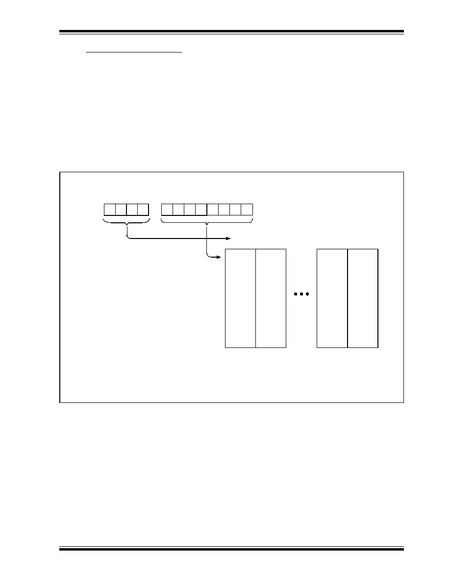
PIC18CXX2
©
7/99 Microchip Technology Inc.
Preliminary
DS39026B-page 47
4.11
Bank Select Register (BSR)
The need for a large general purpose memory space
dictates a RAM banking scheme. The data memory is
partitioned into sixteen banks. When using direct
addressing, the BSR should be configured for the
desired bank.
BSR<3:0> holds the upper 4 bits of the 12-bit RAM
address. The BSR<7:4> bits will always read '0's, and
writes will have no effect.
A
MOVLB
instruction has been provided in the instruc-
tion set to assist in selecting banks.
If the currently selected bank is not implemented, any
read will return all '0's and all writes are ignored. The
STATUS register bits will be set/cleared as appropriate
for the instruction performed.
Each Bank extends up to FFh (256 bytes). All data
memory is implemented as static RAM.
A MOVFF instruction ignores the BSR, since the 12-bit
addresses are embedded into the instruction word.
Section 4.12 provides a description of indirect address-
ing, which allows linear addressing of the entire RAM
space.
FIGURE 4-8:
DIRECT ADDRESSING
Note 1: For register file map detail, see Table 4-1.
2: The access bit of the instruction can be used to force an override of the selected bank
(BSR<3:0>) to the registers of the Access Bank.
3: The MOVFF instruction embeds the entire 12-bit address in the instruction.
Data
Memory
(1)
Direct Addressing
bank select
(2)
location select
(3)
BSR<3:0>
7
0
from opcode
(3)
00h
01h
0Eh
0Fh
Bank 0
Bank 1
Bank 14
Bank 15
1FFh
100h
0FFh
000h
EFFh
E00h
FFFh
F00h

DS39026B-page 48
Preliminary
©
7/99 Microchip Technology Inc.
PIC18CXX2
4.12
Indirect Addressing, INDF and FSR
Registers
Indirect addressing is a mode of addressing data mem-
ory, where the data memory address in the instruction
is not fixed. An SFR register is used as a pointer to the
data memory location that is to be read or written.
Since this pointer is in RAM, the contents can be mod-
ified by the program. This can be useful for data tables
in the data memory and for software stacks. Figure 4-9
shows the operation of indirect addressing. This shows
the moving of the value to the data memory address
specified by the value of the FSR register.
Indirect addressing is possible by using one of the
INDF registers. Any instruction using the INDF register
actually accesses the register pointed to by the File
Select Register, FSR. Reading the INDF register itself
indirectly (FSR = '0') will read 00h. Writing to the INDF
register indirectly results in a no-operation. The FSR
register contains a 12-bit address, which is shown in
Figure 4-10.
The INDFn register is not a physical register. Address-
ing INDFn actually addresses the register whose
address is contained in the FSRn register (FSRn is a
pointer). This is indirect addressing.
Example 4-4 shows a simple use of indirect addressing
to clear the RAM in Bank1 (locations 100h-1FFh) in a
minimum number of instructions.
EXAMPLE 4-4:
HOW TO CLEAR RAM
(BANK1) USING INDIRECT
ADDRESSING
There are three indirect addressing registers. To
address the entire data memory space (4096 bytes),
these registers are 12-bit wide. To store the 12-bits of
addressing information, two 8-bit registers are
required. These indirect addressing registers are:
1.
FSR0: composed of FSR0H:FSR0L
2.
FSR1: composed of FSR1H:FSR1L
3.
FSR2: composed of FSR2H:FSR2L
In addition, there are registers INDF0, INDF1 and
INDF2, which are not physically implemented. Reading
or writing to these registers activates indirect address-
ing, with the value in the corresponding FSR register
being the address of the data.
If an instruction writes a value to INDF0, the value will
be written to the address pointed to by FSR0H:FSR0L.
A read from INDF1 reads the data from the address
pointed to by FSR1H:FSR1L. INDFn can be used in
code anywhere an operand can be used.
If INDF0, INDF1 or INDF2 are read indirectly via an
FSR, all '0's are read (zero bit is set). Similarly, if
INDF0, INDF1 or INDF2 are written to indirectly, the
operation will be equivalent to a
NOP
instruction and the
STATUS bits are not affected.
4.12.1
INDIRECT ADDRESSING OPERATION
Each FSR register has an INDF register associated
with it, plus four additional register addresses. Per-
forming an operation on one of these five registers
determines how the FSR will be modified during indi-
rect addressing.
When data access is done to one of the five INDFn
locations, the address selected will configure the FSRn
register to:
∑ Do nothing to FSRn after an indirect access (no
change) - INDFn
∑ Auto-decrement FSRn after an indirect access
(post-decrement) - POSTDECn
∑ Auto-increment FSRn after an indirect access
(post-increment) - POSTINCn
∑ Auto-increment FSRn before an indirect access
(pre-increment) - PREINCn
∑ Use the value in the WREG register as an offset
to FSRn. Do not modify the value of the WREG or
the FSRn register after an indirect access (no
change) - PLUSWn
When using the auto-increment or auto-decrement
features, the effect on the FSR is not reflected in the
STATUS register. For example, if the indirect address
causes the FSR to equal '0', the Z bit will not be set.
Incrementing or decrementing an FSR affects all 12
bits. That is, when FSRnL overflows from an increment,
FSRnH will be incremented automatically.
Adding these features allows the FSRn to be used as a
stack pointer in addition to its uses for table operations
in data memory.
Each FSR has an address associated with it that per-
forms an indexed indirect access. When a data access
to this INDFn location (PLUSWn) occurs, the FSRn is
configured to add the signed value in the WREG regis-
ter and the value in FSR to form the address before an
indirect access. The FSR value is not changed.
If an FSR register contains a value that points to one of
the INDFn, an indirect read will read 00h (zero bit is
set), while an indirect write will be equivalent to a
NOP
(STATUS bits are not affected).
If an indirect addressing operation is done where the
target address is an FSRnH or FSRnL register, the
write operation will dominate over the pre- or post-
increment/decrement functions.
LFSR 0x100, FSR0 ;
NEXT CLRF POSTINC0 ; Clear INDF register
; & inc pointer
BTFSS FSR0H, 1 ; All done w/ Bank1?
GOTO NEXT ; NO, clear next
CONTINUE ;
: ; YES, continue
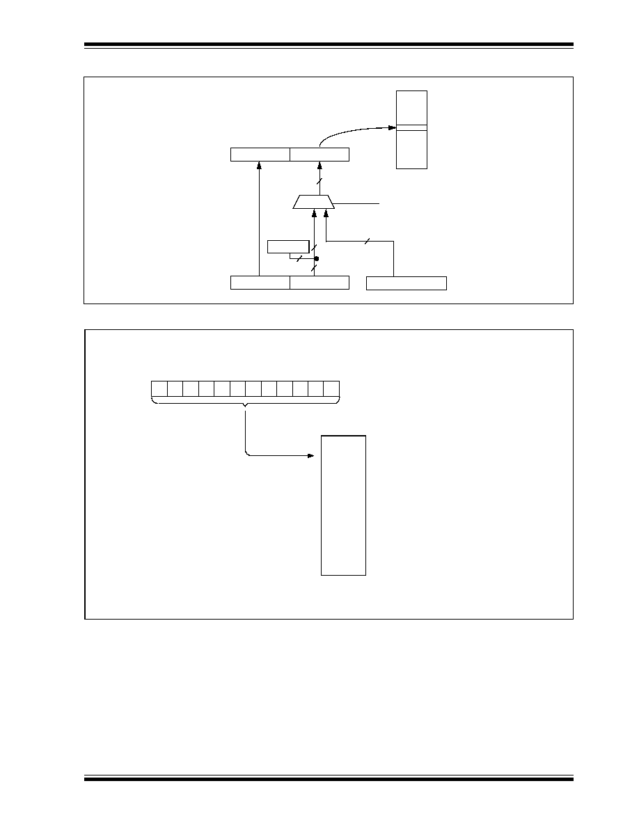
PIC18CXX2
©
7/99 Microchip Technology Inc.
Preliminary
DS39026B-page 49
FIGURE 4-9:
INDIRECT ADDRESSING OPERATION
FIGURE 4-10: INDIRECT ADDRESSING
Opcode
Address
File Address = access of an indirect addressing register
FSR
Instruction
Executed
Instruction
Fetched
RAM
Opcode
File
12
12
12
BSR<3:0>
8
4
0h
FFFh
Note 1: For register file map detail, see Table 4-1.
Data
Memory
(1)
Indirect Addressing
FSR register
11
0
0FFFh
0000h
location select
DS39026B-page 50
Preliminary
©
7/99 Microchip Technology Inc.
PIC18CXX2
4.13
STATUS Register
The STATUS register, shown in Register 4-2, contains
the arithmetic status of the ALU. The STATUS register
can be the destination for any instruction, as with any
other register. If the STATUS register is the destination
for an instruction that affects the Z, DC, C, OV or N bits,
then the write to these five bits is disabled. These bits
are set or cleared according to the device logic. There-
fore, the result of an instruction with the STATUS regis-
ter as destination may be different than intended.
For example,
CLRF STATUS
will clear the upper-three
bits and set the Z bit. This leaves the STATUS register
as
000u u1uu
(where
u
= unchanged).
It is recommended, therefore, that only
BCF, BSF,
SWAPF, MOVFF
and
MOVWF
instructions are used to
alter the STATUS register, because these instruc-
tions do not affect the
Z, C, DC, OV
or
N
bits from
the STATUS register. For other instructions not
affecting any status bits, see Table 19-2.
Register 4-2:
STATUS Register
Note:
The C and DC bits operate as a borrow and
digit borrow bit respectively, in subtraction.
U-0
U-0
U-0
R/W-x
R/W-x
R/W-x
R/W-x
R/W-x
--
--
--
N
OV
Z
DC
C
bit 7
bit 0
bit 7:5
Unimplemented: Read as '0'
bit 4
N: Negative bit
This bit is used for signed arithmatic (2's complement). It indicates whether the result was neg-
ative, (ALU MSB = 1)
1
= Result was negative
0
= Result was positive
bit 3
OV: Overflow bit
This bit is used for signed arithmetic (2's complement). It indicates an overflow of the 7-bit mag-
nitude, which causes the sign bit (bit7) to change state.
1
= Overflow occurred for signed arithmatic (in this arithmetic operation)
0
= No overflow occurred
bit2
Z: Zero bit
1
= The result of an arithmetic or logic operation is zero
0
= The result of an arithmetic or logic operation is not zero
bit 1
DC: Digit carry/borrow bit
For
ADDWF, ADDLW, SUBLW
,
and
SUBWF
instructions
1
= A carry-out from the 4th low order bit of the result occurred
0
= No carry-out from the 4th low order bit of the result
Note:
For borrow, the polarity is reversed. A subtraction is executed by adding the two's
complement of the second operand. For rotate (
RRF
,
RLF
) instructions, this bit is
loaded with either the bit 4 or bit 3 of the source register.
bit 0
C: Carry/borrow bit
For
ADDWF, ADDLW, SUBLW
,
and
SUBWF
instructions
1
= A carry-out from the most significant bit of the result occurred
0
= No carry-out from the most significant bit of the result occurred
Note:
For borrow, the polarity is reversed. A subtraction is executed by adding the two's
complement of the second operand. For rotate (
RRF, RLF
) instructions, this bit is
loaded with either the high or low order bit of the source register.
Legend:
R = Readable bit
W = Writable bit
U = Unimplemented bit, read as `0'
- n = Value at POR reset
'1' = Bit is set
'0' = Bit is cleared
x = Bit is unknown
PIC18CXX2
©
7/99 Microchip Technology Inc.
Preliminary
DS39026B-page 51
4.13.1
RCON REGISTER
The Reset Control (RCON) register contains flag bits,
that allow differentiation between the sources of a
device reset. These flags include the TO, PD, POR,
BOR and RI bits. This register is readable and writable.
Register 4-3:
RCON Register
Note 1: If the BOREN configuration bit is set, BOR
is '1' on Power-on Reset. If the BOREN
configuration bit is clear, BOR is unknown
on Power-on Reset.
The BOR status bit is a "don't care" and is
not necessarily predictable if the brown-
out circuit is disabled (the BOREN config-
uration bit is clear). BOR must then be set
by the user and checked on subsequent
resets to see if it is clear, indicating a
brown-out has occurred.
2: It is recommended that the POR bit be set
after a Power-on Reset has been
detected, so that subsequent Power-on
Resets may be detected.
R/W-0
R/W-0
U-0
R/W-1
R/W-1
R/W-1
R/W-0
R/W-0
IPEN
LWRT
--
RI
TO
PD
POR
BOR
bit 7
bit 0
bit 7
IPEN: Interrupt Priority Enable bit
1
= Enable priority levels on interrupts
0
= Disable priority levels on interrupts (16CXXX compatibility mode)
bit 6
LWRT: Long Write Enable bit
1
= Enable
TBLWT
to internal program memory
Once this bit is set, it can only be cleared by a POR or MCLR reset.
0
= Disable
TBLWT
to internal program memory;
TBLWT
only to external program memory
bit 5
Unimplemented: Read as '0'
bit 4
RI: Reset Instruction Flag bit
1
= The Reset instruction was not executed
0
= The Reset instruction was executed causing a device reset
(must be set in software after a Brown-out Reset occurs)
bit 3
TO: Watchdog Time-out Flag bit
1
= After power-up,
CLRWDT
instruction, or
SLEEP
instruction
0
= A WDT time-out occurred
bit 2
PD: Power-down Detection Flag bit
1
= After power-up or by the
CLRWDT
instruction
0
= By execution of the
SLEEP
instruction
bit 1
POR: Power-on Reset Status bit
1
= A Power-on Reset has not occurred
0
= A Power-on Reset occurred
(must be set in software after a Power-on Reset occurs)
bit 0
BOR: Brown-out Reset Status bit
1
= A Brown-out Reset has not occurred
0
= A Brown-out Reset occurred
(must be set in software after a Brown-out Reset occurs)
Legend:
R = Readable bit
W = Writable bit
U = Unimplemented bit, read as `0'
- n = Value at POR reset
'1' = Bit is set
'0' = Bit is cleared
x = Bit is unknown

DS39026B-page 52
Preliminary
©
7/99 Microchip Technology Inc.
PIC18CXX2
NOTES:
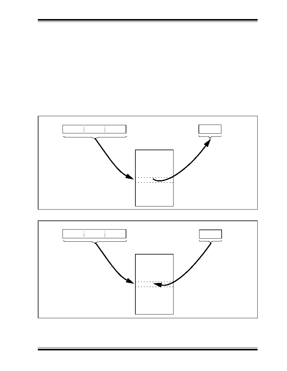
PIC18CXX2
©
7/99 Microchip Technology Inc.
Preliminary
DS39026B-page 53
5.0
TABLE READS/TABLE WRITES
Enhanced devices have two memory spaces: the pro-
gram memory space and the data memory space. The
program memory space is 16 bits wide, while the data
memory space is 8 bits wide. Table Reads and Table
Writes have been provided to move data between
these two memory spaces through an 8 bit register
(TABLAT).
The operations that allow the processor to move data
between the data and program memory spaces are:
∑ Table Read (
TBLRD
)
∑ Table Write (
TBLWT
)
Table Read operations retrieve data from program
memory and place it into the Data memory space.
Figure 5-1 shows the operation of a Table Read with
program and data memory.
Table Write operations store data from the data mem-
ory space into program memory. Figure 5-2 shows the
operation of a Table Write with program and data mem-
ory.
Table operations work with byte entities. A table block
containing data is not required to be word aligned, so a
table block can start and end at any byte address. If a
table write is being used to write an executable program
to program memory, program instructions will need to
be word aligned.
FIGURE 5-1:
TABLE READ OPERATION
FIGURE 5-2:
TABLE WRITE OPERATION
TABLE POINTER
(1)
TABLE LATCH (8-bit)
PROGRAM MEMORY
TBLPTRH
TBLPTRL
TABLAT
TBLPTRU
Instruction:
TBLRD
*
Note 1: Table Pointer points to a byte in
program memory
Program Memory
(TBLPTR)
TABLE POINTER
(1)
TABLE LATCH (8-bit)
PROGRAM MEMORY
TBLPTRH
TBLPTRL
TABLAT
Program Memory
(TBLPTR)
TBLPTRU
Instruction:
TBLWT
*
Note 1: Table Pointer points to a byte in
program memory
DS39026B-page 54
Preliminary
©
7/99 Microchip Technology Inc.
PIC18CXX2
5.1
Control Registers
Several control registers are used in conjunction with
the
TBLRD
and
TBLWT
instructions. These include the:
∑ TBLPTR registers
∑ TABLAT register
∑ RCON register
5.1.1
RCON REGISTER
The LWRT bit specifies the operation of Table Writes to
internal memory when the V
PP
voltage is applied to the
MCLR pin. When the LWRT bit is set, the controller
continues to execute user code, but long table writes
are allowed (for programming internal program mem-
ory) from user mode. The LWRT bit can be cleared only
by performing either a POR or MCLR reset.
Register 5-1:
RCON Register (Address: 08h)
R/W-0
R/W-0
U-0
R/W-1
R/W-1
R/W-1
R/W-0
R/W-0
IPEN
LWRT
--
RI
TO
PD
POR
BOR
bit 7
bit 0
bit 7
IPEN: Interrupt Priority Enable
1
= Enable priority levels on interrupts
0
= Disable priority levels on interrupts (16CXXX compatibility mode)
bit 6
LWRT: Long Write Enable
1
= Enable TBLWT to internal program memory
0
= Disable TBLWT to internal program memory.
Note 1: Only cleared on a POR or MCLR reset.
This bit has no effect on
TBLWTs
to external program memory.
bit 5
Unimplemented: Read as '0'
bit 4
RI: Reset Instruction Flag bit
1
= No Reset instruction occurred
0
= A Reset instruction occurred
bit 3
TO: Time-out bit
1
= After power-up,
CLRWDT
instruction, or
SLEEP
instruction
0
= A WDT time-out occurred
bit 2
PD: Power-down bit
1
= After power-up or by the
CLRWDT
instruction
0
= By execution of the
SLEEP
instruction
bit 1
POR: Power-on Reset Status bit
1
= No Power-on Reset occurred
0
= A Power-on Reset occurred (must be set in software after a Power-on Reset occurs)
bit 0
BOR: Brown-out Reset Status bit
1
= No Brown-out Reset nor POR reset occurred
0
= A Brown-out Reset nor POR reset occurred
(must be set in software after a Brown-out Reset occurs)
Legend:
R = Readable bit
W = Writable bit
U = Unimplemented bit, read as `0'
- n = Value at POR reset
'1' = Bit is set
'0' = Bit is cleared
x = Bit is unknown

PIC18CXX2
©
7/99 Microchip Technology Inc.
Preliminary
DS39026B-page 55
5.1.2
TABLAT - TABLE LATCH REGISTER
The Table Latch (TABLAT) is an 8-bit register mapped
into the SFR space. The Table Latch is used to hold
8-bit data during data transfers between program
memory and data memory.
5.1.3
TBLPTR - TABLE POINTER REGISTER
The Table Pointer (TBLPTR) addresses a byte within
the program memory. The TBLPTR is comprised of
three SFR registers (Table Pointer Upper byte, High
byte and Low byte). These three registers (TBLP-
TRU:TBLPTRH:TBLPTRL) join to form a 22-bit wide
pointer. The low order 21-bits allow the device to
address up to 2M bytes of program memory space. The
22nd bit allows access to the Device ID, the User ID
and the Configuration bits.
The table pointer TBLPTR is used by the TBLRD and
TBLWT instructions. These instructions can update
the TBLPTR in one of four ways based on the table
operation. These operations are shown in Table 5-1.
These operations on the TBLPTR only affect the low
order 21-bits.
TABLE 5-1:
TABLE POINTER OPERATIONS WITH TBLRD AND TBLWT INSTRUCTIONS
Example
Operation on Table Pointer
TBLRD*
TBLWT*
TBLPTR is not modified
TBLRD*+
TBLWT*+
TBLPTR is incremented after the read/write
TBLRD*-
TBLWT*-
TBLPTR is decremented after the read/write
TBLRD+*
TBLWT+*
TBLPTR is incremented before the read/write
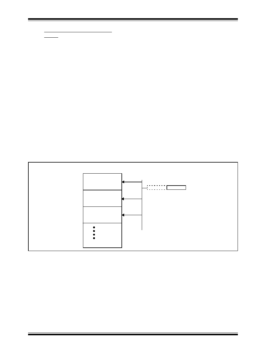
DS39026B-page 56
Preliminary
©
7/99 Microchip Technology Inc.
PIC18CXX2
5.2
Internal Program Memory Read/
Writes
5.2.1
TABLE READ OVERVIEW (TBLRD)
The
TBLRD
instructions are used to read data from pro-
gram memory to data memory.
TBLPTR points to a byte address in program space.
Executing
TBLRD
places the byte pointed to into TAB-
LAT. In addition, TBLPTR can be modified automati-
cally for the next Table Read operation.
Table Reads from program memory are performed one
byte at a time. The instruction will load TABLAT with the
one byte from program memory pointed to by TBLPTR.
5.2.2
INTERNAL PROGRAM MEMORY WRITE
BLOCK SIZE
The internal program memory of PIC18CXXX devices
is written in blocks. For PIC18CXX2 devices, the write
block size is 2 bytes. Consequently, Table Write oper-
ations to internal program memory are performed in
pairs, one byte at a time.
When a Table Write occurs to an even program mem-
ory address (TBLPTR<0> = 0), the contents of TABLAT
are transferred to an internal holding register. This is
performed as a short write and the program memory
block is not actually programmed at this time. The hold-
ing register is not accessible by the user.
When a Table Write occurs to an odd program memory
address (TBLPTR,)>=1), a long write is started. During
the long write, the contents of TABLAT are written to the
high byte of the program memory block and the con-
tents of the holding register are transferred to the low
byte of the program memory block.
Figure 5-3 shows the holding register and the program
memory write blocks.
If a single byte is to be programmed, the low (even) byte
of the destination program word should be read using
TBLRD
*, modified or changed, if required, and written
back to the same address using
TBLWT*+
. The high
(odd) byte should be read using
TBLRD*
, modified or
changed if required, and written back to the same
address using
TBLWT
. The write to an odd address will
cause a long write to begin. This process ensures that
existing data in either byte will not be changed unless
desired.
FIGURE 5-3:
HOLDING REGISTER AND THE WRITE BLOCK
Block n
Block n + 1
Block n + 2
MSB
The write to the MSB of the Write Block
causes the entire block to be written to pro-
gram memory. The program memory block
that is written depends on the address that is
written to in the MSB of the Write Block.
Holding Register
Program Memory (x 2-bits)
Write Block

PIC18CXX2
©
7/99 Microchip Technology Inc.
Preliminary
DS39026B-page 57
5.2.2.1
OPERATION
The long write is what actually programs words of data
into the internal memory. When a
TBLWT
to the MSB of
the write block occurs, instruction execution is halted.
During this time, programming voltage and the data
stored in internal latches is applied to program memory.
For a long write to occur:
1.
MCLR/V
PP
pin must be at the programming volt-
age
2.
LWRT bit must be set
3.
TBLWT to the address of the MSB of the write
block
If the LWRT bit is clear, a short write will occur and pro-
gram memory will not be changed. If the
TBLWT
is not
to the MSB of the write block, then the programming
phase is not initiated.
Setting the LWRT bit enables long writes when the
MCLR pin is taken to V
PP
voltage. Once the LWRT bit
is set, it can be cleared only by performing a POR or
MCLR reset.
To ensure that the memory location has been well pro-
grammed, a minimum programming time is required.
The long write can be terminated after the program-
ming time has expired by a reset or an interrupt. Having
only one interrupt source enabled to terminate the long
write ensures that no unintended interrupts will prema-
turely terminate the long write.
5.2.2.2
SEQUENCE OF EVENTS
The sequence of events for programming an internal
program memory location should be:
1.
Enable the interrupt that terminates the long
write. Disable all other interrupts.
2.
Clear the source interrupt flag.
3.
If Interrupt Service Routine execution is desired
when the device wakes, enable global inter-
rupts.
4.
Set LWRT bit in the RCON register.
5.
Raise MCLR/V
PP
pin to the programming volt-
age, V
PP
.
6.
Clear the WDT (if enabled).
7.
Set the interrupt source to interrupt at the
required time.
8.
Execute the table write for the lower (even) byte.
This will be a short write.
9.
Execute the table write for the upper (odd) byte.
This will be a long write. The controller will go to
sleep while programming. The interrupt wakes
the controller.
10. If GIE was set, service the interrupt request.
11. Lower MCLR/V
PP
pin to V
DD
.
12. Verify the memory location (table read).

DS39026B-page 58
Preliminary
©
7/99 Microchip Technology Inc.
PIC18CXX2
5.2.3
INTERRUPTS
The long write must be terminated by a reset or any
interrupt.
The interrupt source must have its interrupt enable bit
set. When the source sets its interrupt flag, program-
ming will terminate. This will occur regardless of the
settings of interrupt priority bits, the GIE/GIEH bit or the
PIE/GIEL bit.
Depending on the states of interrupt priority bits, the
GIE/GIEH bit or the PIE/GIEL bit, program execution
can either be vectored to the high or low priority Inter-
rupt Service Routine (ISR) or continue execution from
where programming commenced.
In either case, the interrupt flag will not be cleared
when programming is terminated and will need to be
cleared by the software.
TABLE 5-2:
SLEEP MODE, INTERRUPT ENABLE BITS AND INTERRUPT RESULTS
GIE/
GIEH
PIE/
GIEL
Priority
Interrupt
Enable
Interrupt
Flag
Action
X
X
X
0
(default)
X
Long write continues even if interrupt
flag becomes set during sleep.
X
X
X
1
0
Long write continues, will wake when
the interrupt flag is set.
0
(default)
0
(default)
X
1
1
Terminates long write,
executes next instruction. Interrupt flag
not cleared.
0
(default)
1
1
high priority
(default)
1
1
Terminates long write,
executes next instruction. Interrupt flag
not cleared.
1
0
(default)
0
low
1
1
Terminates long write, executes next
instruction. Interrupt flag not cleared.
0
(default)
1
0
low
1
1
Terminates long write, branches to low
priority interrupt vector.
Interrupt flag can be cleared by ISR.
1
0
(default)
1
high priority
(default)
1
1
Terminates long write, branches to high
priority interrupt vector.
Interrupt flag can be cleared by ISR.

PIC18CXX2
©
7/99 Microchip Technology Inc.
Preliminary
DS39026B-page 59
5.2.4
UNEXPECTED TERMINATION OF WRITE
OPERATIONS
If a write is terminated by an unplanned event such as
loss of power, an unexpected reset, or an interrupt that
was not disabled, the memory location just pro-
grammed should be verified and reprogrammed if
needed.

DS39026B-page 60
Preliminary
©
7/99 Microchip Technology Inc.
PIC18CXX2
NOTES:

PIC18CXX2
©
7/99 Microchip Technology Inc.
Preliminary
DS39026B-page 61
6.0
8 X 8 HARDWARE MULTIPLIER
6.1
Introduction
An 8 x 8 hardware multiplier is included in the ALU of
the PIC18CXX2 devices. By making the multiply a
hardware operation, it completes in a single instruction
cycle. This is an unsigned multiply that gives a 16-bit
result. The result is stored into the 16-bit product regis-
ter pair (PRODH:PRODL). The multiplier does not
affect any flags in the ALUSTA register.
Making the 8 x 8 multiplier execute in a single cycle
gives the following advantages:
∑ Higher computational throughput
∑ Reduces code size requirements for multiply algo-
rithms
The performance increase allows the device to be used
in applications previously reserved for Digital Signal
Processors.
Table 6-1 shows a performance comparison between
enhanced devices using the single cycle hardware mul-
tiply, and performing the same function without the
hardware multiply.
TABLE 6-1:
PERFORMANCE COMPARISON
Routine
Multiply Method
Program
Memory
(Words)
Cycles
(Max)
Time
@ 40 MHz
@ 10 MHz
@ 4 MHz
8 x 8 unsigned
Without hardware multiply
13
69
6.9
µ
s
27.6
µ
s
69
µ
s
Hardware multiply
1
1
100 ns
400 ns
1
µ
s
8 x 8 signed
Without hardware multiply
33
91
9.1
µ
s
36.4
µ
s
91
µ
s
Hardware multiply
6
6
600 ns
2.4
µ
s
6
µ
s
16 x 16 unsigned
Without hardware multiply
21
242
24.2
µ
s
96.8
µ
s
242
µ
s
Hardware multiply
24
24
2.4
µ
s
9.6
µ
s
24
µ
s
16 x 16 signed
Without hardware multiply
52
254
25.4
µ
s
102.6
µ
s
254
µ
s
Hardware multiply
36
36
3.6
µ
s
14.4
µ
s
36
µ
s

PIC18CXX2
DS39026B-page 62
Preliminary
©
7/99 Microchip Technology Inc.
6.2
Operation
Example 6-1 shows the sequence to do an 8 x 8
unsigned multiply. Only one instruction is required
when one argument of the multiply is already loaded in
the WREG register.
Example 6-2 shows the sequence to do an 8 x 8 signed
multiply. To account for the sign bits of the arguments,
each argument's most significant bit (MSb) is tested
and the appropriate subtractions are done.
EXAMPLE 6-1:
8 x 8 UNSIGNED MULTIPLY
ROUTINE
EXAMPLE 6-2:
8 x 8 SIGNED MULTIPLY
ROUTINE
Example 6-3 shows the sequence to do a 16 x 16
unsigned multiply. Equation 6-1 shows the algorithm
that is used. The 32-bit result is stored in 4 registers
RES3:RES0.
EQUATION 6-1:
16 x 16 UNSIGNED
MULTIPLICATION
ALGORITHM
RES3:RES0
=
ARG1H:ARG1L
∑
ARG2H:ARG2L
=
(ARG1H
∑
ARG2H
∑
2
16
)+
(ARG1H
∑
ARG2L
∑
2
8
)+
(ARG1L
∑
ARG2H
∑
2
8
)+
(ARG1L
∑
ARG2L)
EXAMPLE 6-3:
16 x 16 UNSIGNED
MULTIPLY ROUTINE
Example 6-4 shows the sequence to do an 16 x 16
signed multiply. Equation 6-2 shows the algorithm
used. The 32-bit result is stored in four registers
RES3:RES0. To account for the sign bits of the argu-
ments, each argument pairs most significant bit (MSb)
is tested and the appropriate subtractions are done.
EQUATION 6-2:
16 x 16 SIGNED
MULTIPLICATION
ALGORITHM
RES3:RES0
=
ARG1H:ARG1L
∑
ARG2H:ARG2L
=
(ARG1H
∑
ARG2H
∑
2
16
)+
(ARG1H
∑
ARG2L
∑
2
8
)+
(ARG1L
∑
ARG2H
∑
2
8
)+
(ARG1L
∑
ARG2L)+
(-1
∑
ARG2H<7>
∑
ARG1H:ARG1L
∑
2
16
)+
(-1
∑
ARG1H<7>
∑
ARG2H:ARG2L
∑
2
16
)
MOVFF ARG1, WREG ;
MULWF ARG2 ; ARG1 * ARG2 ->
; PRODH:PRODL
MOVFF ARG1, WREG
MULWF ARG2 ; ARG1 * ARG2 ->
; PRODH:PRODL
BTFSC ARG2, SB ; Test Sign Bit
SUBWF PRODH, F ; PRODH = PRODH
; - ARG1
MOVFF ARG2, WREG
BTFSC ARG1, SB ; Test Sign Bit
SUBWF PRODH, F ; PRODH = PRODH
; - ARG2
MOVFF ARG1L, WREG
MULWF ARG2L ; ARG1L * ARG2L ->
; PRODH:PRODL
MOVFF PRODH, RES1 ;
MOVFF PRODL, RES0 ;
;
MOVFF ARG1H, WREG
MULWF ARG2H ; ARG1H * ARG2H ->
; PRODH:PRODL
MOVFF PRODH, RES3 ;
MOVFF PRODL, RES2 ;
;
MOVFF ARG1L, WREG
MULWF ARG2H ; ARG1L * ARG2H ->
; PRODH:PRODL
MOVFF PRODL, WREG ;
ADDWF RES1, F ; Add cross
MOVFF PRODH, WREG ; products
ADDWFC RES2, F ;
CLRF WREG, F ;
ADDWFC RES3, F ;
;
MOVFF ARG1H, WREG ;
MULWF ARG2L ; ARG1H * ARG2L ->
; PRODH:PRODL
MOVFF PRODL, WREG ;
ADDWF RES1, F ; Add cross
MOVFF PRODH, WREG ; products
ADDWFC RES2, F ;
CLRF WREG, F ;
ADDWFC RES3, F ;

PIC18CXX2
©
7/99 Microchip Technology Inc.
Preliminary
DS39026B-page 63
EXAMPLE 6-4:
16 x 16 SIGNED MULTIPLY
ROUTINE
MOVFF ARG1L, WREG
MULWF ARG2L ; ARG1L * ARG2L ->
; PRODH:PRODL
MOVFF PRODH, RES1 ;
MOVFF PRODL, RES0 ;
;
MOVFF ARG1H, WREG
MULWF ARG2H ; ARG1H * ARG2H ->
; PRODH:PRODL
MOVFF PRODH, RES3 ;
MOVFF PRODL, RES2 ;
;
MOVFF ARG1L, WREG
MULWF ARG2H ; ARG1L * ARG2H ->
; PRODH:PRODL
MOVFF PRODL, WREG ;
ADDWF RES1, F ; Add cross
MOVFF PRODH, WREG ; products
ADDWFC RES2, F ;
CLRF WREG, F ;
ADDWFC RES3, F ;
;
MOVFF ARG1H, WREG ;
MULWF ARG2L ; ARG1H * ARG2L ->
; PRODH:PRODL
MOVFF PRODL, WREG ;
ADDWF RES1, F ; Add cross
MOVFF PRODH, WREG ; products
ADDWFC RES2, F ;
CLRF WREG, F ;
ADDWFC RES3, F ;
;
BTFSS ARG2H, 7 ; ARG2H:ARG2L neg?
GOTO SIGN_ARG1 ; no, check ARG1
MOVFF ARG1L, WREG ;
SUBWF RES2 ;
MOVFF ARG1H, WREG ;
SUBWFB RES3
;
SIGN_ARG1
BTFSS ARG1H, 7 ; ARG1H:ARG1L neg?
GOTO CONT_CODE ; no, done
MOVFF ARG2L, WREG ;
SUBWF RES2 ;
MOVFF ARG2H, WREG ;
SUBWFB RES3
;
CONT_CODE
:

PIC18CXX2
DS39026B-page 64
Preliminary
©
7/99 Microchip Technology Inc.
NOTES:

PIC18CXX2
©
7/99 Microchip Technology Inc.
Preliminary
DS39026B-page 65
7.0
INTERRUPTS
The PIC18CXX2 devices have multiple interrupt
sources and an interrupt priority feature that allows
each interrupt source to be assigned a high priority
level or a low priority level. The high priority interrupt
vector is at 000008h and the low priority interrupt vector
is at 000018h. High priority interrupt events will over-
ride any low priority interrupts that may be in progress.
There are ten registers which are used to control inter-
rupt operation. These registers are:
∑ RCON
∑ INTCON
∑ INTCON2
∑ INTCON3
∑ PIR1, PIR2
∑ PIE1, PIE2
∑ IPR1, IPR2
It is recommended that the Microchip header files sup-
plied with MPLAB be used for the symbolic bit names
in these registers. This allows the assembler/compiler
to automatically take care of the placement of these bits
within the specified register.
Each interrupt source has three bits to control its oper-
ation. The functions of these bits are:
∑ Flag bit to indicate that an interrupt event
occurred
∑ Enable bit that allows program execution to
branch to the interrupt vector address when
the flag bit is set
∑ Priority bit to select high priority or low priority
The interrupt priority feature is enabled by setting the
IPEN bit (RCON<7>). When interrupt priority is
enabled, there are two bits which enable interrupts glo-
bally. Setting the GIEH bit (INTCON<7>) enables all
interrupts that have the priority bit set. Setting the GIEL
bit (INTCON<6>) enables all interrupts that have the
priority bit cleared. When the interrupt flag, enable bit
and appropriate global interrupt enable it are set, the
interrupt will vector immediately to address 000008h or
000018h depending on the priority level. Individual
interrupts can be disabled through their corresponding
enable bits.
When the IPEN bit is cleared (default state), the inter-
rupt priority feature is disabled and interrupts are com-
patible with PICmicro mid-range devices. In
compatibility mode, the interrupt priority bits for each
source have no effect. INTCON<6> is the PEIE bit,
which enables/disables all peripheral interrupt sources.
INTCON<7> is the GIE bit, which enables/disables all
interrupt sources. All interrupts branch to address
000008h in compatibility mode.
When an interrupt is responded to, the Global Interrupt
Enable bit is cleared to disable further interrupts. If the
IPEN bit is cleared, this is the GIE bit. If interrupt prior-
ity levels are used, this will be either the GIEH or GIEL
bit. High priority interrupt sources can interrupt a low
priority interrupt.
The return address is pushed onto the stack and the
PC is loaded with the interrupt vector address
(000008h or 000018h). Once in the interrupt service
routine, the source(s) of the interrupt can be deter-
mined by polling the interrupt flag bits. The interrupt
flag bits must be cleared in software before re-enabling
interrupts to avoid recursive interrupts.
The "return from interrupt" instruction, RETFIE, exits
the interrupt routine and sets the GIE bit (GIEH or GIEL
if priority levels are used), which re-enables interrupts.
For external interrupt events, such as the INT pins or
the PORTB input change interrupt, the interrupt latency
will be three to four instruction cycles. The exact
latency is the same for one or two cycle instructions.
Individual interrupt flag bits are set regardless of the
status of their corresponding enable bit or the GIE bit.
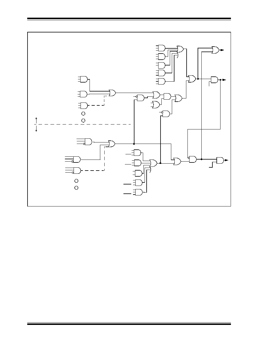
PIC18CXX2
DS39026B-page 66
Preliminary
©
7/99 Microchip Technology Inc.
FIGURE 7-1:
INTERRUPT LOGIC
T0IE
GIEH/GIE
GIEL/PEIE
Wake-up if in SLEEP mode
Interrupt to CPU
Vector to location
0008h
INT2F
INT2E
INT2P
INT1F
INT1E
INT1P
T0IF
T0IE
T0IP
INT0F
INT0E
RBIF
RBIE
RBIP
IPE
T0IF
T0IP
INT1F
INT1E
INT1P
INT2F
INT2E
INT2P
RBIF
RBIE
RBIP
INT0F
INT0E
GIEL\PEIE
Interrupt to CPU
Vector to Location
IPE
IPE
0018h
Peripheral Interrupt Flag bit
Peripheral Interrupt Enable bit
Peripheral Interrupt Priority bit
Peripheral Interrupt Flag bit
Peripheral Interrupt Enable bit
Peripheral Interrupt Priority bit
TMR1IF
TMR1IE
TMR1IP
XXXXIF
XXXXIE
XXXXIP
Additional Peripheral Interrupts
TMR1IF
TMR1IE
TMR1IP
High Priority Interrupt Generation
Low Priority Interrupt Generation
XXXXIF
XXXXIE
XXXXIP
Additional Peripheral Interrupts

PIC18CXX2
©
7/99 Microchip Technology Inc.
Preliminary
DS39026B-page 67
7.0.1
INTCON REGISTERS
The INTCON Registers are readable and writable
registers, which contains various enable, priority and
flag bits.
Register 7-1:
INTCON Register
R/W-0
R/W-0
R/W-0
R/W-0
R/W-0
R/W-0
R/W-0
R/W-x
GIE/GIEH
PEIE/GIEL
TMR0IE
INT0IE
RBIE
TMR0IF
INT0IF
RBIF
bit 7
bit 0
bit 7
GIE/GIEH: Global Interrupt Enable bit
When IPEN = 0:
1
= Enables all un-masked interrupts
0
= Disables all interrupts
When IPEN = 1:
1
= Enables all interrupts
0
= Disables all interrupts
bit 6
PEIE/GEIL: Peripheral Interrupt Enable bit
When IPEN = 0:
1
= Enables all un-masked peripheral interrupts
0
= Disables all peripheral interrupts
When IPEN = 1:
1
= Enables all low priority peripheral interrupts
0
= Disables all priority peripheral interrupts
bit 5
TMR0IE: TMR0 Overflow Interrupt Enable bit
1
= Enables the TMR0 overflow interrupt
0
= Disables the TMR0 overflow interrupt
bit 4
INT0IE: INT0 External Interrupt Enable bit
1
= Enables the INT0 external interrupt
0
= Disables the INT0 external interrupt
bit 3
RBIE: RB Port Change Interrupt Enable bit
1
= Enables the RB port change interrupt
0
= Disables the RB port change interrupt
bit 2
TMR0IF: TMR0 Overflow Interrupt Flag bit
1
= TMR0 register has overflowed (must be cleared in software)
0
= TMR0 register did not overflow
bit 1
INT0IF: INT0 External Interrupt Flag bit
1
= The INT0 external interrupt occurred (must be cleared in software)
0
= The INT0 external interrupt did not occur
bit 0
RBIF: RB Port Change Interrupt Flag bit
1
= At least one of the RB7:RB4 pins changed state (must be cleared in software)
0
= None of the RB7:RB4 pins have changed state
Legend:
R = Readable bit
W = Writable bit
U = Unimplemented bit, read as `0'
- n = Value at POR reset
'1' = Bit is set
'0' = Bit is cleared
x = Bit is unknown
Note:
Interrupt flag bits get set when an interrupt condition occurs, regardless of the state
of its corresponding enable bit or the global enable bit. User software should ensure
the appropriate interrupt flag bits are clear prior to enabling an interrupt. This feature
allows for software polling.

PIC18CXX2
DS39026B-page 68
Preliminary
©
7/99 Microchip Technology Inc.
Register 7-2:
INTCON2 Register
R/W-1
R/W-1
R/W-1
R/W-1
U-0
R/W-1
U-0
R/W-1
RBPU
INTEDG0
INTEDG1
INTEDG2
--
TMR0IP
--
RBIP
bit 7
bit 0
bit 7
RBPU: PORTB Pull-up Enable bit
1
= All PORTB pull-ups are disabled
0
= PORTB pull-ups are enabled by individual port latch values
bit 6
INTEDG0:External Interrupt0 Edge Select bit
1
= Interrupt on rising edge
0
= Interrupt on falling edge
bit 5
INTEDG1: External Interrupt1 Edge Select bit
1
= Interrupt on rising edge
0
= Interrupt on falling edge
bit 4
INTEDG2: External Interrupt2 Edge Select bit
1
= Interrupt on rising edge
0
= Interrupt on falling edge
bit 3
Unimplemented: Read as '0'
bit 2
TMR0IP: TMR0 Overflow Interrupt Priority bit
1
= High priority
0
= Low priority
bit 1
Unimplemented: Read as '0'
bit 0
RBIP: RB Port Change Interrupt Priority bit
1
= High priority
0
= Low priority
Legend:
R = Readable bit
W = Writable bit
U = Unimplemented bit, read as `0'
- n = Value at POR reset
'1' = Bit is set
'0' = Bit is cleared
x = Bit is unknown
Note:
Interrupt flag bits get set when an interrupt condition occurs, regardless of the state
of its corresponding enable bit or the global enable bit. User software should ensure
the appropriate interrupt flag bits are clear prior to enabling an interrupt. This feature
allows for software polling.

PIC18CXX2
©
7/99 Microchip Technology Inc.
Preliminary
DS39026B-page 69
Register 7-3:
INTCON3 Register
R/W-1
R/W-1
U-0
R/W-0
R/W-0
U-0
R/W-0
R/W-0
INT2IP
INT1IP
--
INT2IE
INT1IE
--
INT2IF
INT1IF
bit 7
bit 0
bit 7
INT2IP: INT2 External Interrupt Priority bit
1
=High priority
0
=Low priority
bit 6
INT1IP: INT1 External Interrupt Priority bit
1
=High priority
0
=Low priority
bit 5
Unimplemented: Read as '0'
bit 4
INT2IE: INT2 External Interrupt Enable bit
1
=Enables the INT2 external interrupt
0
=Disables the INT2 external interrupt
bit 3
INT1IE: INT1 External Interrupt Enable bit
1
=Enables the INT1 external interrupt
0
=Disables the INT1 external interrupt
bit 2
Unimplemented: Read as '0'
bit 1
INT2IF: INT2 External Interrupt Flag bit
1
=The INT2 external interrupt occurred
(must be cleared in software)
0
=The INT2 external interrupt did not occur
bit 0
INT1IF: INT1 External Interrupt Flag bit
1
=The INT1 external interrupt occurred
(must be cleared in software)
0
=The INT1 external interrupt did not occur
Legend:
R = Readable bit
W = Writable bit
U = Unimplemented bit, read as `0'
- n = Value at POR reset
'1' = Bit is set
'0' = Bit is cleared
x = Bit is unknown
Note:
Interrupt flag bits get set when an interrupt condition occurs, regardless of the state
of its corresponding enable bit or the global enable bit. User software should ensure
the appropriate interrupt flag bits are clear prior to enabling an interrupt. This feature
allows for software polling.
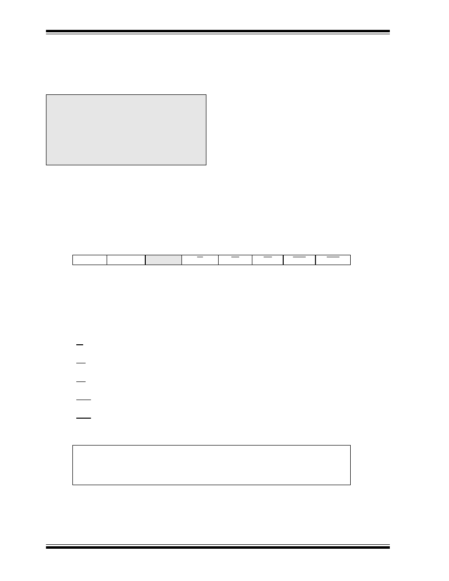
PIC18CXX2
DS39026B-page 70
Preliminary
©
7/99 Microchip Technology Inc.
7.0.2
PIR REGISTERS
The PIR registers contain the individual flag bits for the
peripheral interrupts. Due to he number of peripheral
interrupt sources, there are two Peripheral Interrupt
Flag Registers (PIR1, PIR2).
7.0.3
PIE REGISTERS
The PIE registers contain the individual enable bits for
the peripheral interrupts. Due to the number of periph-
eral interrupt sources, there are two Peripheral Inter-
rupt Enable Registers (PIE1, PIE2). When IPEN = 0,
the PEIE bit must be set to enable any of these periph-
eral interrupts.
7.0.4
IPR REGISTERS
The IPR registers contain the individual priority bits for
the peripheral interrupts. Due to on the number of
peripheral interrupt sources, there are two Peripheral
Interrupt Priority Registers (IPR1, IPR2). The operation
of the priority bits requires that the Interrupt Priority
Enable (IPEN) bit be set.
7.0.5
RCON REGISTER
The RCON register contains the bit which is used to
enable prioritized interrupts (IPEN).
Register 7-4:
RCON Register
Note 1: Interrupt flag bits get set when an interrupt
condition occurs, regardless of the state of
its corresponding enable bit or the global
enable bit, GIE (INTCON<7>).
Note 2: User software should ensure the appropri-
ate interrupt flag bits are cleared prior to
enabling an interrupt, and after servicing
that interrupt.
R/W-0
R/W-0
U-0
R/W-1
R/W-1
R/W-1
R/W-0
R/W-0
IPEN
LWRT
--
RI
TO
PD
POR
BOR
bit 7
bit 0
bit 7
IPEN: Interrupt Priority Enable bit
1
= Enable priority levels on interrupts
0
= Disable priority levels on interrupts (16CXXX compatibility mode)
bit 6
LWRT: Long Write Enable
For details of bit operation see Register 4-1
bit 5
Unimplemented: Read as '0'
bit 4
RI: Reset Instruction Flag bit
For details of bit operation see Register 4-1
bit 3
TO: Watchdog Time-out Flag bit
For details of bit operation see Register 4-1
bit 2
PD: Power-down Detection Flag bit
For details of bit operation see Register 4-1
bit 1
POR: Power-on Reset Status bit
For details of bit operation see Register 4-1
bit 0
BOR: Brown-out Reset Status bit
For details of bit operation see Register 4-1
Legend:
R = Readable bit
W = Writable bit
U = Unimplemented bit, read as `0'
- n = Value at POR reset
'1' = Bit is set
'0' = Bit is cleared
x = Bit is unknown

PIC18CXX2
©
7/99 Microchip Technology Inc.
Preliminary
DS39026B-page 71
Register 7-5:
Peripheral Interrupt Request (Flag) Registers
R/W-0
R/W-0
R-0
R-0
R/W-0
R/W-0
R/W-0
R/W-0
PIR1
PSPIF
ADIF
RCIF
TXIF
SSPIF
CCP1IF
TMR2IF
TMR1IF
bit 7
bit 0
U-0
U-0
U-0
U-0
R/W-0
R/W-0
R/W-0
R/W-0
PIR2
--
--
--
--
BCLIF
LVDIF
TMR3IF
CCP2IF
bit 7
bit 0
PIR1
bit 7
PSPIF: Parallel Slave Port Read/Write Interrupt Flag bit
1
= A read or a write operation has taken place
(must be cleared in software)
0
= No read or write has occurred
bit 6
ADIF: A/D Converter Interrupt Flag bit
1
= An A/D conversion completed
(must be cleared in software)
0
= The A/D conversion is not complete
bit 5
RCIF: USART Receive Interrupt Flag bit
1
= The USART receive buffer, RCREG, is full
(cleared when RCREG is read)
0
= The USART receive buffer is empty
bit 4
TXIF: USART Transmit Interrupt Flag bit
1
= The USART transmit buffer, TXREG, is empty
(cleared when TXREG is written)
0
= The USART transmit buffer is full
bit 3
SSPIF: Master Synchronous Serial Port Interrupt Flag bit
1
= The transmission/reception is complete
(must be cleared in software)
0
= Waiting to transmit/receive
bit 2
CCP1IF: CCP1 Interrupt Flag bit
Capture Mode
1
= A TMR1 register capture occurred
(must be cleared in software)
0
= No TMR1 register capture occurred
Compare Mode
1
= A TMR1 register compare match occurred
(must be cleared in software)
0
= No TMR1 register compare match occurred
PWM Mode
Unused in this mode
bit 1
TMR2IF: TMR2 to PR2 Match Interrupt Flag bit
1
= TMR2 to PR2 match occurred
(must be cleared in software)
0
= No TMR2 to PR2 match occurred
bit 0
TMR1IF: TMR1 Overflow Interrupt Flag bit
1
= TMR1 register overflowed
(must be cleared in software)
0
= TMR1 register did not overflow

PIC18CXX2
DS39026B-page 72
Preliminary
©
7/99 Microchip Technology Inc.
Register 7-5:
Peripheral Interrupt Request (Flag) Registers (cont'd)
PIR2
bit 7-4
Unimplemented: Read as '0'
bit 3
BCLIF: Bus Collision Interrupt Flag bit
1
= A Bus Collision occurred
(must be cleared in software)
0
= No Bus Collision occurred
bit 2
LVDIF: Low-Voltage Detect Interrupt Flag bit
1
= A low voltage condition occurred
(must be cleared in software)
0
= The device voltage is above the Low Voltage Detect trip point
bit 1
TMR3IF: TMR3 Overflow Interrupt Flag bit
1
= TMR3 register overflowed
(must be cleared in software)
0
= TMR3 register did not overflow
bit 0
CCP2IF: CCPx Interrupt Flag bit
Capture Mode
1
= A TMR1 register capture occurred
(must be cleared in software)
0
= No TMR1 register capture occurred
Compare Mode
1
= A TMR1 register compare match occurred
(must be cleared in software)
0
= No TMR1 register compare match occurred
PWM Mode
Unused in this mode
Legend:
R = Readable bit
W = Writable bit
U = Unimplemented bit, read as `0'
- n = Value at POR reset
'1' = Bit is set
'0' = Bit is cleared
x = Bit is unknown

PIC18CXX2
©
7/99 Microchip Technology Inc.
Preliminary
DS39026B-page 73
Register 7-6:
Peripheral Interrupt Enable Registers
R/W-0
R/W-0
R/W-0
R/W-0
R/W-0
R/W-0
R/W-0
R/W-0
PIE1
PSPIE
ADIE
RCIE
TXIE
SSPIE
CCP1IE
TMR2IE
TMR1IE
bit 7
bit 0
U-0
U-0
U-0
U-0
R/W-0
R/W-0
R/W-0
R/W-0
PIE2
--
--
--
--
BCLIE
LVDIE
TMR3IE
CCP2IE
bit 7
bit 0
PIE1
bit 7
PSPIE: Parallel Slave Port Read/Write Interrupt Enable bit
1
= Enables the PSP read/write interrupt
0
= Disables the PSP read/write interrupt
bit 6
ADIE: A/D Converter Interrupt Enable bit
1
= Enables the A/D interrupt
0
= Disables the A/D interrupt
bit 5
RCIE: USART Receive Interrupt Enable bit
1
= Enables the USART receive interrupt
0
= Disables the USART receive interrupt
bit 4
TXIE: USART Transmit Interrupt Enable bit
1
= Enables the USART transmit interrupt
0
= Disables the USART transmit interrupt
bit 3
SSPIE: Master Synchronous Serial Port Interrupt Enable bit
1
= Enables the MSSP interrupt
0
= Disables the MSSP interrupt
bit 2
CCP1IE: CCP1 Interrupt Enable bit
1
= Enables the CCP1 interrupt
0
= Disables the CCP1 interrupt
bit 1
TMR2IE: TMR2 to PR2 Match Interrupt Enable bit
1
= Enables the TMR2 to PR2 match interrupt
0
= Disables the TMR2 to PR2 match interrupt
bit 0
TMR1IE: TMR1 Overflow Interrupt Enable bit
1
= Enables the TMR1 overflow interrupt
0
= Disables the TMR1 overflow interrupt
PIE2
bit 7-4
Unimplemented: Read as '0'
bit 3
BCLIE: Bus Collision Interrupt Enable bit
1
= Enabled
0
= Disabled
bit 2
LVDIE: Low-voltage Detect Interrupt Enable bit
1
= Enabled
0
= Disabled
bit 1
TMR3IE: TMR3 Overflow Interrupt Enable bit
1
= Enables the TMR3 overflow interrupt
0
= Disables the TMR3 overflow interrupt
bit 0
CCP2IE: CCP2 Interrupt Enable bit
1
= Enables the CCP2 interrupt
0
= Disables the CCP2 interrupt
Legend:
R = Readable bit
W = Writable bit
U = Unimplemented bit, read as `0'
- n = Value at POR reset
'1' = Bit is set
'0' = Bit is cleared
x = Bit is unknown

PIC18CXX2
DS39026B-page 74
Preliminary
©
7/99 Microchip Technology Inc.
Register 7-7:
Peripheral Interrupt Priority Registers
R/W-1
R/W-1
R/W-1
R/W-1
R/W-1
R/W-1
R/W-1
R/W-1
IPR1
PSPIP
ADIP
RCIP
TXIP
SSPIP
CCP1IP
TMR2IP
TMR1IP
bit 7
bit 0
U-0
U-0
U-0
U-0
R/W-1
R/W-1
R/W-1
R/W-1
IPR2
--
--
--
--
BCLIP
LVDIP
TMR3IP
CCP2IP
bit 7
bit 0
IPR1
bit 7
PSPIP: Parallel Slave Port Read/Write Interrupt Priority bit
1
= High priority
0
= Low priority
bit 6
ADIP: A/D Converter Interrupt Priority bit
1
= High priority
0
= Low priority
bit 5
RCIP: USART Receive Interrupt Priority bit
1
= High priority
0
= Low priority
bit 4
TXIP: USART Transmit Interrupt Priority bit
1
= High priority
0
= Low priority
bit 3
SSPIP: Master Synchronous Serial Port Interrupt Priority bit
1
= High priority
0
= Low priority
bit 2
CCP1IP: CCP1 Interrupt Priority bit
1
= High priority
0
= Low priority
bit 1
TMR2IP: TMR2 to PR2 Match Interrupt Priority bit
1
= High priority
0
= Low priority
bit 0
TMR1IP: TMR1 Overflow Interrupt Priority bit
1
= High priority
0
= Low priority
IPR2
bit 7-4
Unimplemented: Read as '0'
bit 3
BCLIP: Bus Collision Interrupt Priority bit
1
= High priority
0
= Low priority
bit 2
LVDIP: Low-voltage Detect Interrupt Priority bit
1
= High priority
0
= Low priority
bit 1
TMR3IP: TMR3 Overflow Interrupt Priority bit
1
= High priority
0
= Low priority
bit 0
CCP2IP: CCP2 Interrupt Priority bit
1
= High priority
0
= Low priority
Legend:
R = Readable bit
W = Writable bit
U = Unimplemented bit, read as `0'
- n = Value at POR reset
'1' = Bit is set
'0' = Bit is cleared
x = Bit is unknown

PIC18CXX2
©
7/99 Microchip Technology Inc.
Preliminary
DS39026B-page 75
7.0.6
INT0 INTERRUPT
External interrupts on the RB0/INT0, RB1/INT1 and
RB2/INT2 pins are edge triggered: either rising if the
corresponding INTEDGx bit is set in the INTCON2 reg-
ister, or falling, if the INTEDGx bit is clear. When a valid
edge appears on the RBx/INTx pin, the corresponding
flag bit INTxF is set. This interrupt can be disabled by
clearing the corresponding enable bit INTxE. Flag bit
INTxF must be cleared in software in the interrupt ser-
vice routine before re-enabling the interrupt. All exter-
nal interrupts (INT0, INT1 and INT2) can wake-up the
processor from SLEEP, if bit INTxE was set prior to
going into SLEEP. If the global interrupt enable bit GIE
set, the processor will branch to the interrupt vector fol-
lowing wake-up.
Interrupt priority for INT1 and INT2 is determined by the
value contained in the interrupt priority bits INT1IP
(INTCON3<6>) and INT2IP (INTCON3<7>). There is
no priority bit associated with INT0. It is always a high
priority interrupt source.
7.0.7
TMR0 INTERRUPT
In 8-bit mode (which is the default), an overflow (FFh
00h) in the TMR0 register will set flag bit TMR0IF. In
16-bit mode, an overflow (FFFFh
0000h) in the
TMR0H:TMR0L registers will set flag bit TMR0IF. The
interrupt can be enabled/disabled by setting/clearing
enable bit T0IE (INTCON<5>). Interrupt priority for
Timer0 is determined by the value contained in the
interrupt priority bit TMR0IP (INTCON2<2>). See Sec-
tion 8.0 for further details on the Timer0 module.
7.0.8
PORTB INTERRUPT ON CHANGE
An input change on PORTB<7:4> sets flag bit RBIF
(INTCON<0>). The interrupt can be enabled/disabled
by setting/clearing enable bit RBIE (INTCON<3>).
Interrupt priority for PORTB Interrupt on change is
determined by the value contained in the interrupt pri-
ority bit RBIP (INTCON2<0>).
7.1
Context Saving During Interrupts
During an interrupt, the return PC value is saved on the
stack. Additionally, the WREG, STATUS and BSR reg-
isters are saved on the fast return stack. If a fast return
from interrupt is not used (See Section 4.3), the user
may need to save the WREG, STATUS and BSR regis-
ters in software. Depending on the user's application,
other registers may also need to be saved. Example 6-
1 saves and restores the WREG, STATUS and BSR
registers during an interrupt service routine.
EXAMPLE 7-1:
SAVING STATUS, WREG AND BSR REGISTERS IN RAM
MOVWF
W_TEMP
; W_TEMP is in virtual bank
MOVFF
STATUS, STATUS_TEMP
; STATUS_TEMP located anywhere
MOVFF
BSR, BSR_TEMP
; BSR located anywhere
;
; USER ISR CODE
;
MOVFF
BSR_TEMP, BSR
; Restore BSR
MOVF
W_TEMP, W
; Restore WREG
MOVFF
STATUS_TEMP, STATUS
; Restore STATUS

PIC18CXX2
DS39026B-page 76
Preliminary
©
7/99 Microchip Technology Inc.
NOTES:

PIC18CXX2
©
7/99 Microchip Technology Inc.
Preliminary
DS39026B-page 77
8.0
I/O PORTS
Depending on the device selected, there are either five
ports or three ports available. Some pins of the I/O
ports are multiplexed with an alternate function from
the peripheral features on the device. In general, when
a peripheral is enabled, that pin may not be used as a
general purpose I/O pin.
Each port has three registers for its operation. These
registers are:
∑ TRIS register (Data Direction register)
∑ PORT register (reads the levels on the pins of the
device)
∑ LAT register (output latch)
The data latch (LAT register) is useful for read-modify-
write operations on the value that the I/O pins are driv-
ing.
8.1
PORTA, TRISA and LATA Registers
PORTA is a 6-bit wide bi-directional port. The corre-
sponding data direction register is TRISA. Setting a
TRISA bit (=1) will make the corresponding PORTA pin
an input, (i.e., put the corresponding output driver in a
hi-impedance mode). Clearing a TRISA bit (=0) will
make the corresponding PORTA pin an output, (i.e., put
the contents of the output latch on the selected pin).
Reading the PORTA register reads the status of the
pins, whereas writing to it will write to the port latch.
The Data Latch register (LATA) is also memory
mapped. Read-modify-write operations on the LATA
register reads and writes the latched output value for
PORTA.
The RA4 pin is multiplexed with the Timer0 module
clock input to become the RA4/T0CKI pin. The RA4/
T0CKI pin is a Schmitt Trigger input and an open drain
output. All other RA port pins have TTL input levels and
full CMOS output drivers.
The other PORTA pins are multiplexed with analog
inputs and the analog V
REF
+ and V
REF
- inputs. The
operation of each pin is selected by clearing/setting the
control bits in the ADCON1 register (A/D Control
Register1).
The TRISA register controls the direction of the RA
pins, even when they are being used as analog inputs.
The user must ensure the bits in the TRISA register are
maintained set when using them as analog inputs.
EXAMPLE 8-1:
INITIALIZING PORTA
Note:
On a Power-on Reset, these pins are con-
figured as inputs and read as '0'.
Note:
On a Power-on Reset, these pins are con-
figured as analog inputs and read as '0'.
CLRF PORTA
;
Initialize PORTA by
; clearing output
; data latches
CLRF LATA
; Alternate method
; to clear output
; data latches
MOVLW 0x07
; Configure A/D
MOVWF ADCON1
; for digital inputs
MOVLW
0xCF
;
Value used to
; initialize data
; direction
MOVWF
TRISA
;
Set RA<3:0> as inputs
;
RA<5:4> as outputs
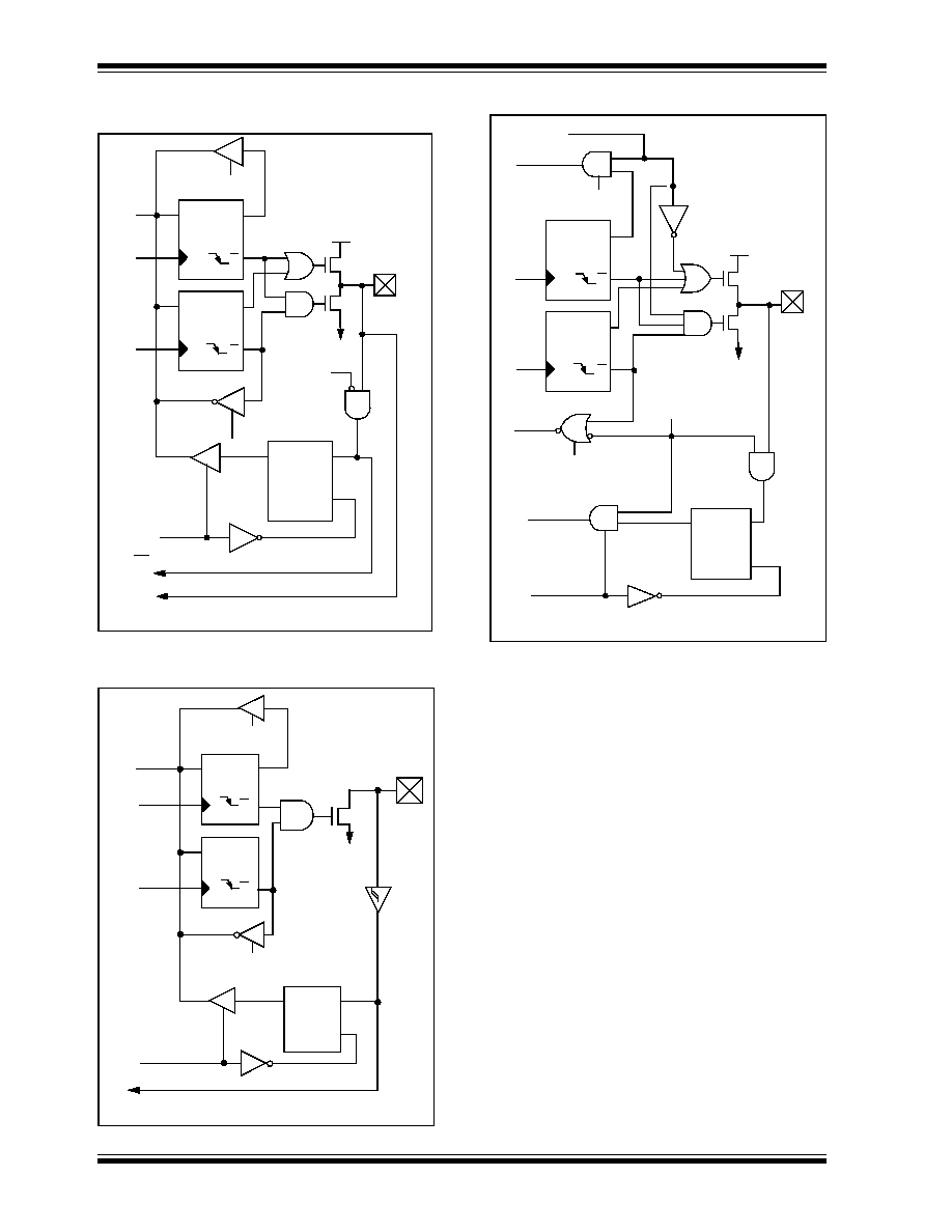
PIC18CXX2
DS39026B-page 78
Preliminary
©
7/99 Microchip Technology Inc.
FIGURE 8-1:
BLOCK DIAGRAM OF
RA3:RA0 AND RA5 PINS
FIGURE 8-2:
BLOCK DIAGRAM OF RA4/
T0CKI PIN
FIGURE 8-3:
BLOCK DIAGRAM OF RA6
Data
Bus
Q
D
Q
CK
Q
D
Q
CK
Q
D
EN
P
N
WR LATA
WR TRISA
Data Latch
TRIS Latch
RD TRISA
RD PORTA
V
SS
V
DD
I/O pin
(1)
Note 1:
I/O pins have protection diodes to V
DD
and V
SS
.
Analog
input
mode
TTL
input
buffer
To A/D Converter and LVD Modules
RD LATA
or
PORTA
SS input (RA5 only)
Data
Bus
WR TRISA
RD PORTA
Data Latch
TRIS Latch
RD TRISA
Schmitt
Trigger
input
buffer
N
V
SS
I/O pin
(1)
TMR0 Cock Input
Note 1: I/O pin has protection diodes to V
SS
only.
Q
D
Q
CK
Q
D
Q
CK
EN
Q
D
EN
RD LATA
WR LATA
or
PORTA
Data
Bus
Q
D
Q
CK
Q
D
Q
CK
Q
D
EN
P
N
WR LATA
WR
Data Latch
TRIS Latch
RD TRISA
RD PORTA
V
SS
V
DD
I/O pin
(1)
Note 1:
I/O pins have protection diodes to V
DD
and V
SS
.
or
PORTA
RD LATA
ECRA6 or
Data Bus
ECRA6 or
enable
Data Bus
TTL
input
buffer
RCRA6
RCRA6 enable
TRISA
PIC18CXX2
©
7/99 Microchip Technology Inc.
Preliminary
DS39026B-page 79
TABLE 8-1:
PORTA FUNCTIONS
TABLE 8-2:
SUMMARY OF REGISTERS ASSOCIATED WITH PORTA
Name
Bit#
Buffer Function
RA0/AN0
bit0
TTL
Input/output or analog input
RA1/AN1
bit1
TTL
Input/output or analog input
RA2/AN2/V
REF
-
bit2
TTL
Input/output or analog input or V
REF
-
RA3/AN3/V
REF
+
bit3
TTL
Input/output or analog input or V
REF
+
RA4/T0CKI
bit4
ST
Input/output or external clock input for Timer0
Output is open drain type
RA5/SS/AN4/LVDIN
bit5
TTL
Input/output or slave select input for synchronous serial port or analog
input, or low voltage detect input
OSC2/CLKO/RA6
bit6
OSC2 or clock output or I/O pin
Legend: TTL = TTL input, ST = Schmitt Trigger input
Name
Bit 7
Bit 6
Bit 5
Bit 4
Bit 3
Bit 2
Bit 1
Bit 0
Value on
POR,
BOR
Value on all
other
resets
PORTA
--
RA6
RA5
RA4
RA3
RA2
RA1
RA0
--0x 0000
--0u 0000
LATA
--
Latch A Data Output Register
--xx xxxx
--uu uuuu
TRISA
--
PORTA Data Direction Register
--11 1111
--11 1111
ADCON1
ADFM
ADCS2
--
--
PCFG3
PCFG2
PCFG1
PCFG0
--0- 0000
--0- 0000
Legend: x = unknown, u = unchanged, - = unimplemented locations read as '0'. Shaded cells are not used by PORTA.
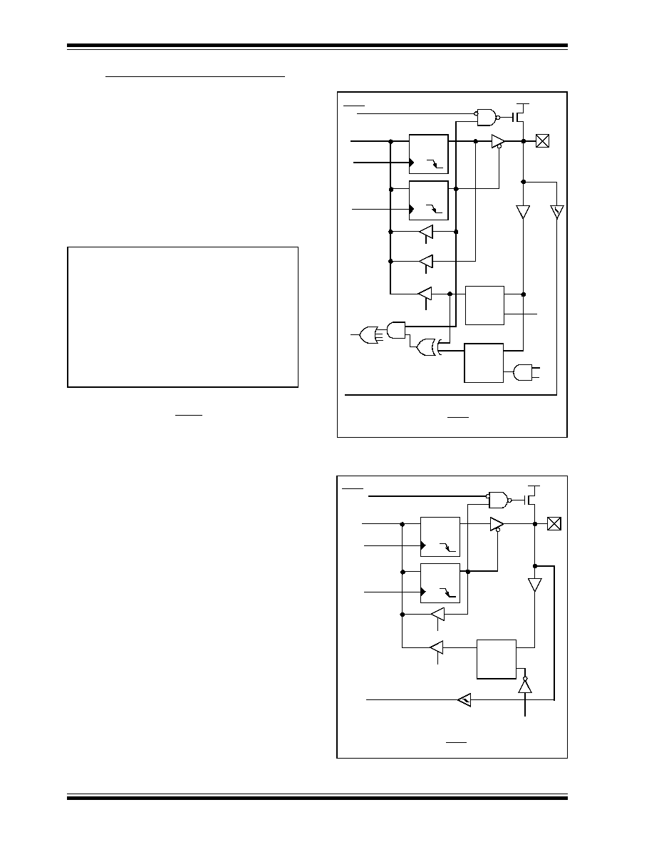
PIC18CXX2
DS39026B-page 80
Preliminary
©
7/99 Microchip Technology Inc.
8.2
PORTB, TRISB and LATB Registers
PORTB is an 8-bit wide bi-directional port. The corre-
sponding data direction register is TRISB. Setting a
TRISB bit (=1) will make the corresponding PORTB pin
an input, (i.e., put the corresponding output driver in a
hi-impedance mode). Clearing a TRISB bit (=0) will
make the corresponding PORTB pin an output, ( i.e. put
the contents of the output latch on the selected pin).
The Data Latch register (LATB) is also memory
mapped. Read-modify-write operations on the LATB
register reads and writes the latched output value for
PORTB.
EXAMPLE 8-2:
INITIALIZING PORTB
Each of the PORTB pins has a weak internal pull-up. A
single control bit can turn on all the pull-ups. This is per-
formed by clearing bit RBPU (INTCON2<7>). The
weak pull-up is automatically turned off when the port
pin is configured as an output. The pull-ups are dis-
abled on a Power-on Reset.
Four of PORTB's pins, RB7:RB4, have an interrupt on
change feature. Only pins configured as inputs can
cause this interrupt to occur (i.e. any RB7:RB4 pin con-
figured as an output is excluded from the interrupt on
change comparison). The input pins (of RB7:RB4) are
compared with the old value latched on the last read of
PORTB. The "mismatch" outputs of RB7:RB4 are
OR'ed together to generate the RB Port Change Inter-
rupt with flag bit RBIF (INTCON<0>).
This interrupt can wake the device from SLEEP. The
user, in the interrupt service routine, can clear the inter-
rupt in the following manner:
a)
Any read or write of PORTB (except with the
MOVFF instruction). This will end the mismatch
condition.
b)
Clear flag bit RBIF.
A mismatch condition will continue to set flag bit RBIF.
Reading PORTB will end the mismatch condition and
allow flag bit RBIF to be cleared.
The interrupt on change feature is recommended for
wake-up on key depression operation and operations
where PORTB is only used for the interrupt on change
feature. Polling of PORTB is not recommended while
using the interrupt on change feature.
FIGURE 8-4:
BLOCK DIAGRAM OF
RB7:RB4 PINS
FIGURE 8-5:
BLOCK DIAGRAM OF
RB2:RB0 PINS
CLRF PORTB
;
Initialize PORTB by
; clearing output
; data latches
CLRF LATB
; Alternate method
; to clear output
; data latches
MOVLW
0xCF
;
Value used to
; initialize data
; direction
MOVWF
TRISB
;
Set RB<3:0> as inputs
;
RB<5:4> as outputs
;
RB<7:6> as inputs
Data Latch
From other
RBPU
(2)
P
V
DD
I/O
Q
D
CK
Q
D
CK
Q
D
EN
Q
D
EN
Data Bus
WR LATB
WR TRISB
Set RBIF
TRIS Latch
RD TRISB
RD PORTB
RB7:RB4 pins
weak
pull-up
RD PORTB
Latch
TTL
Input
Buffer
pin
(1)
ST
Buffer
RBx/INTx
Q3
Q1
RD LATB
or
PORTB
Note 1:
I/O pins have diode protection to V
DD
and V
SS
.
2:
To enable weak pull-ups, set the appropriate TRIS
bit(s) and clear the RBPU bit (INTCON2<7>).
Data Latch
RBPU
(2)
P
V
DD
Q
D
CK
Q
D
CK
Q
D
EN
Data Bus
WR Port
WR TRIS
RD TRIS
RD Port
weak
pull-up
RD Port
RB0/INT
I/O
pin
(1)
TTL
Input
Buffer
Schmitt Trigger
Buffer
TRIS Latch
Note 1:
I/O pins have diode protection to V
DD
and V
SS
.
2:
To enable weak pull-ups, set the appropriate TRIS
bit(s) and clear the RBPU bit (OPTION_REG<7>).
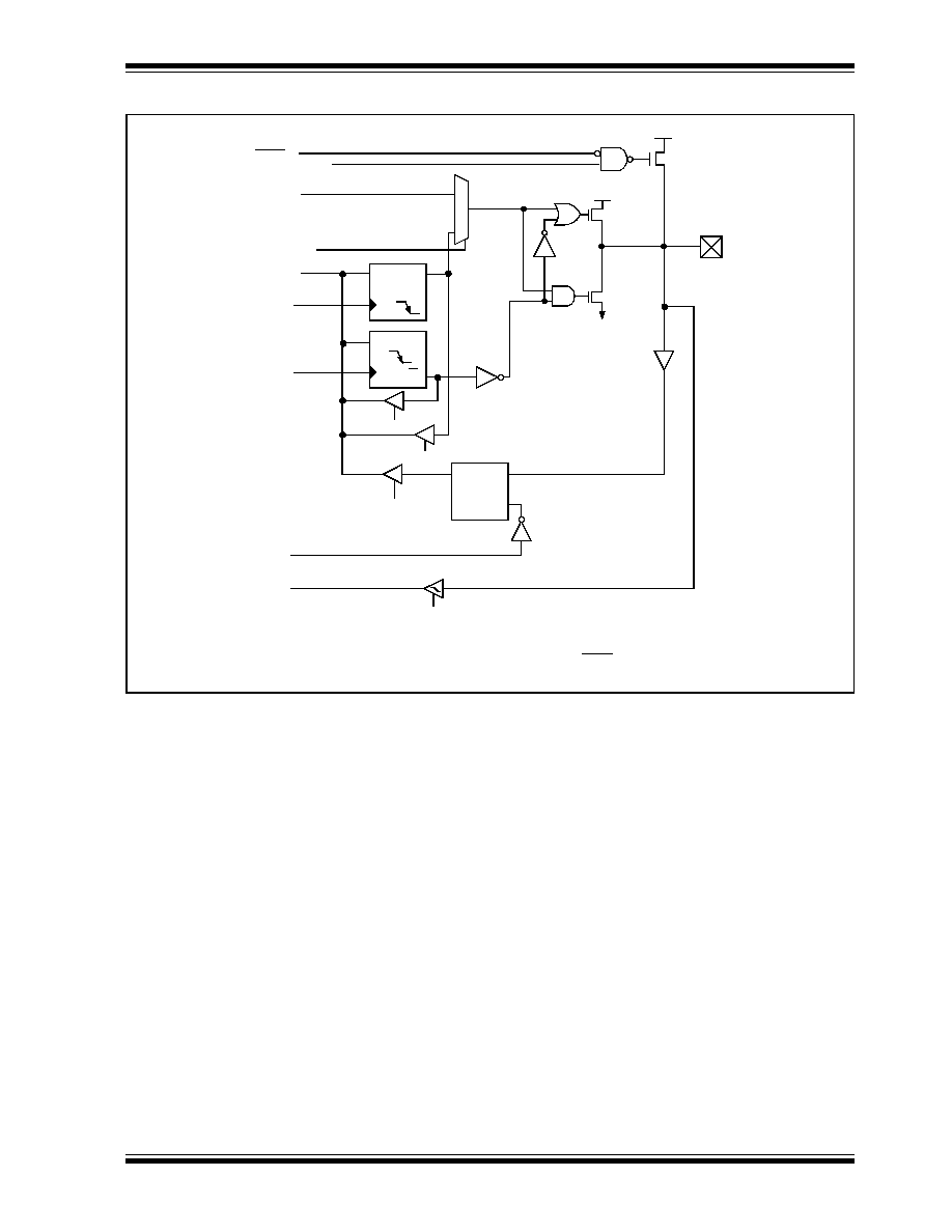
PIC18CXX2
©
7/99 Microchip Technology Inc.
Preliminary
DS39026B-page 81
FIGURE 8-6:
BLOCK DIAGRAM OF RB3
Data Latch
P
V
DD
Q
D
CK
Q
D
EN
Data Bus
WR LATB or
WR TRISB
RD TRISB
RD PORTB
weak
pull-up
CCP2 input
(3)
TTL
Input
Buffer
Schmitt Trigger
Buffer
TRIS Latch
RD LATB
WR PORTB
RBPU
(2)
CK
D
Enable
(3)
CCP Output
RD PORTB
CCP Output
(3)
1
0
P
N
V
DD
V
SS
I/O
Pin
(1)
Q
CCP2MX
CCP2MX = 0
Note 1:
I/O pin has diode protection to V
DD
and V
SS
.
2:
To enable weak pull-ups, set the appropriate DDR bit(s) and clear the RBPU bit (INTCON2<7>).
3:
The CCP2 input/output is multiplexed with RB3 if the CCP2MX bit is enabled (='0') in the configuration register.
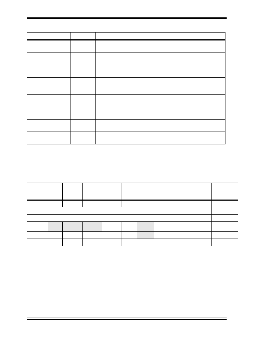
PIC18CXX2
DS39026B-page 82
Preliminary
©
7/99 Microchip Technology Inc.
TABLE 8-3:
PORTB FUNCTIONS
TABLE 8-4:
SUMMARY OF REGISTERS
ASSOCIATED WITH PORTB
Name
Bit#
Buffer Function
RB0/INT0
bit0
TTL/ST
(1)
Input/output pin or external interrupt input1. Internal software
programmable weak pull-up.
RB1/INT1
bit1
TTL/ST
(1)
Input/output pin or external interrupt input2. Internal software programma-
ble weak pull-up.
RB2/INT2
bit2
TTL/ST
(1)
Input/output pin or external interrupt input3. Internal software programma-
ble weak pull-up.
RB3/CCP2
(3)
bit3
TTL/ST
(4)
Input/output pin. Capture2 input/Compare2 output/PWM output when
CCP2MX configuration bit is enabled. Internal software programmable
weak pull-up.
RB4
bit4
TTL
Input/output pin (with interrupt on change). Internal software programma-
ble weak pull-up.
RB5
bit5
TTL
Input/output pin (with interrupt on change). Internal software programma-
ble weak pull-up.
RB6
bit6
TTL/ST
(2)
Input/output pin (with interrupt on change). Internal software programma-
ble weak pull-up. Serial programming clock.
RB7
bit7
TTL/ST
(2)
Input/output pin (with interrupt on change). Internal software programma-
ble weak pull-up. Serial programming data.
Legend: TTL = TTL input, ST = Schmitt Trigger input
Note 1: This buffer is a Schmitt Trigger input when configured as the external interrupt.
2: This buffer is a Schmitt Trigger input when used in serial programming mode.
3: A device configuration bit selects which I/O pin the CCP2 pin is multiplexed on.
4: This buffer is a Schmitt Trigger input when configured as the CCP2 input.
Name
Bit 7
Bit 6
Bit 5
Bit 4
Bit 3
Bit 2
Bit 1
Bit 0
Value on
POR,
BOR
Value on all
other resets
PORTB
RB7
RB6
RB5
RB4
RB3
RB2
RB1
RB0
xxxx xxxx
uuuu uuuu
LATB
LATB Data Output Register
TRISB
PORTB Data Direction Register
1111 1111
1111 1111
INTCON
GIE/
GIEH
PEIE/
GIEL
TMR0IE
INT0IE
RBIE
TMR0IF
INT0IF
RBIF
0000 000x
0000 000u
INTCON2
RBPU
INTEDG0
INTEDG1
INTEDG2
--
TMR0IP
--
RBIP
1111 -1-1
1111 -1-1
INTCON3
INT2IP
INT1IP
--
INT2IE
INT1IE
--
INT2IF
INT1IF
11-0 0-00
11-0 0-00
Legend: x = unknown, u = unchanged. Shaded cells are not used by PORTB.
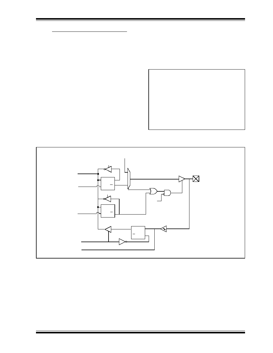
PIC18CXX2
©
7/99 Microchip Technology Inc.
Preliminary
DS39026B-page 83
8.3
PORTC, TRISC and LATC Registers
PORTC is an 8 bit wide bi-directional port. The corre-
sponding Data Direction Register is TRISC. Setting a
TRISC bit (=1) will make the corresponding PORTC pin
an input, (i.e., put the corresponding output driver in a
hi-impedance mode). Clearing a TRISC bit (=0) will
make the corresponding PORTC pin an output, (i.e.,
put the contents of the output latch on the selected pin).
The Data Latch register (LATC) is also memory
mapped. Read-modify-write operations on the LATC
register reads and writes the latched output value for
PORTC.
PORTC is multiplexed with several peripheral functions
(Table 8-5). PORTC pins have Schmitt Trigger input
buffers.
When enabling peripheral functions, care should be
taken in defining TRIS bits for each PORTC pin. Some
peripherals override the TRIS bit to make a pin an out-
put, while other peripherals override the TRIS bit to
make a pin an input. The user should refer to the corre-
sponding peripheral section for the correct TRIS bit set-
tings.
The pin override value is not loaded into the TRIS reg-
ister. This allows read-modify-write of the TRIS register,
without concern due to peripheral overrides.
EXAMPLE 8-3:
INITIALIZING PORTC
FIGURE 8-7:
PORTC BLOCK DIAGRAM (PERIPHERAL OUTPUT OVERRIDE)
CLRF PORTC
;
Initialize PORTC by
; clearing output
; data latches
CLRF LATC
; Alternate method
; to clear output
; data latches
MOVLW
0xCF
;
Value used to
; initialize data
; direction
MOVWF
TRISC
;
Set RC<3:0> as inputs
; RC<5:4> as outputs
;
RC<7:6> as inputs
Data Bus
WR LATC or
WR TRISC
RD TRISC
Q
D
Q
CK
Q
D
CK
Peripheral Data Out
1
0
Q
D
Q
CK
RD PORTC
Peripheral Data In
WR PORTC
RD LATC
Q
Peripheral Out
Select
Peripheral Output Enable
RC7: RC0
ST Buffer
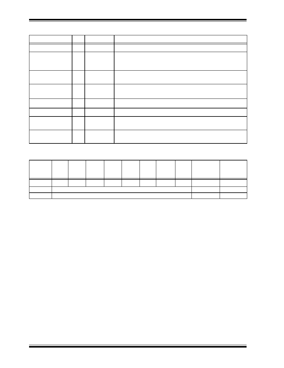
PIC18CXX2
DS39026B-page 84
Preliminary
©
7/99 Microchip Technology Inc.
TABLE 8-5:
PORTC FUNCTIONS
TABLE 8-6:
SUMMARY OF REGISTERS ASSOCIATED WITH PORTC
Name
Bit#
Buffer Type
Function
RC0/T1OSO/T1CKI
bit0
ST
Input/output port pin or Timer1 oscillator output/Timer1 clock input
RC1/T1OSI/CCP2
bit1
ST
Input/output port pin, Timer1 oscillator input, or Capture2 input/
Compare2 output/PWM output when CCP2MX configuration bit is
disabled.
RC2/CCP1
bit2
ST
Input/output port pin or Capture1 input/Compare1 output/PWM1
output
RC3/SCK/SCL
bit3
ST
RC3 can also be the synchronous serial clock for both SPI and I
2
C
modes.
RC4/SDI/SDA
bit4
ST
RC4 can also be the SPI Data In (SPI mode) or data I/O (I
2
C mode).
RC5/SDO
bit5
ST
Input/output port pin or Synchronous Serial Port data output
RC6/TX/CK
bit6
ST
Input/output port pin, Addressable USART Asynchronous Transmit, or
Addressable USART Synchronous Clock
RC7/RX/DT
bit7
ST
Input/output port pin, Addressable USART Asynchronous Receive, or
Addressable USART Synchronous Data
Legend: ST = Schmitt Trigger input
Name
Bit 7
Bit 6
Bit 5
Bit 4
Bit 3
Bit 2
Bit 1
Bit 0
Value on
POR,
BOR
Value on all
other resets
PORTC
RC7
RC6
RC5
RC4
RC3
RC2
RC1
RC0
xxxx xxxx
uuuu uuuu
LATC
LATC Data Output Register
xxxx xxxx
uuuu uuuu
TRISC
PORTC Data Direction Register
1111 1111
1111 1111
Legend: x = unknown, u = unchanged.
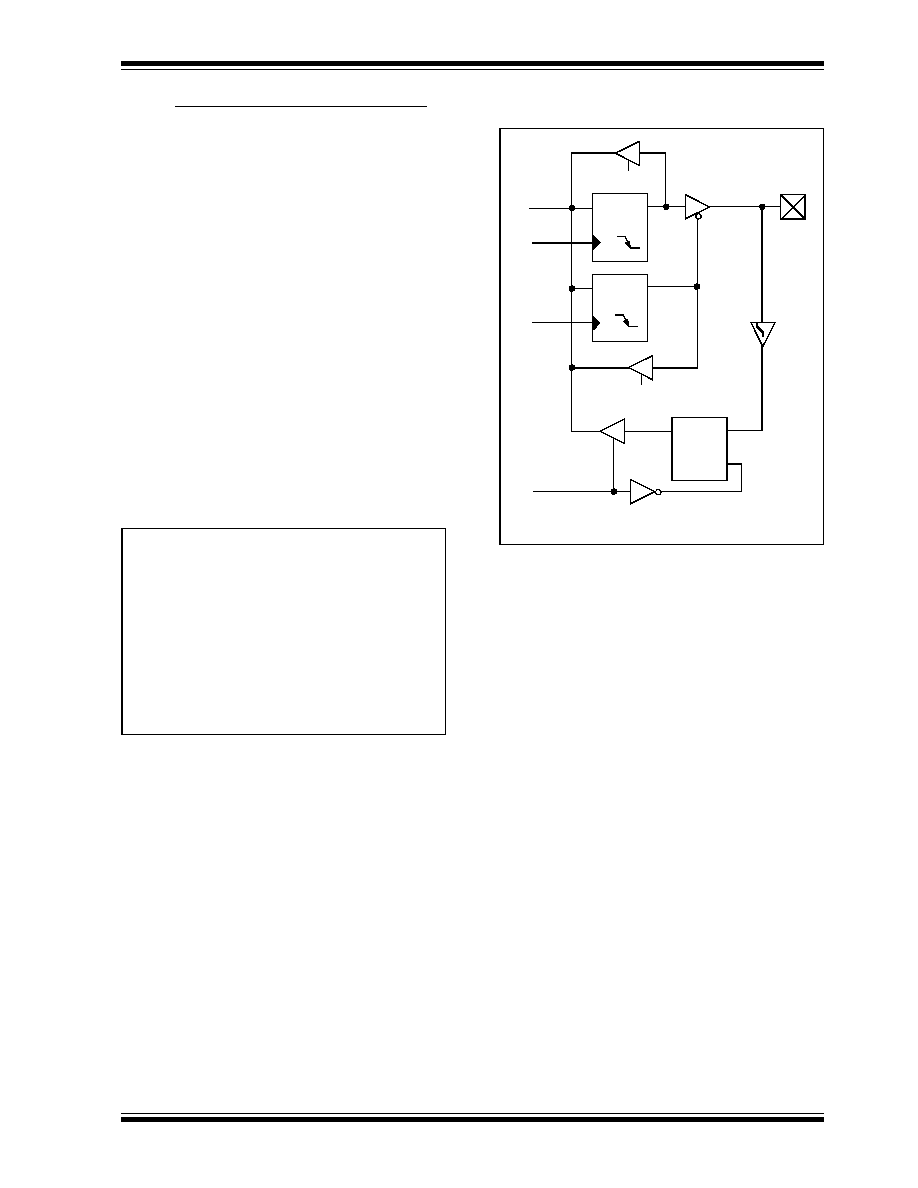
PIC18CXX2
©
7/99 Microchip Technology Inc.
Preliminary
DS39026B-page 85
8.4
PORTD, TRISD and LATD Registers
This section is applicable to only the PIC18C4X2
devices.
PORTD is an 8 bit wide bi-directional port. The corre-
sponding Data Direction Register is TRISD. Setting a
TRISD bit (=1) will make the corresponding PORTD pin
an input, (i.e., put the corresponding output driver in a
hi-impedance mode). Clearing a TRISD bit (=0) will
make the corresponding PORTD pin an output, (i.e.,
put the contents of the output latch on the selected pin).
The Data Latch Register (LATD) is also memory
mapped. Read-modify-write operations on the LATD
register reads and writes the latched output value for
PORTD.
PORTD is an 8-bit port with Schmitt Trigger input buff-
ers. Each pin is individually configurable as an input or
output.
PORTD can be configured as an 8-bit wide micropro-
cessor port (parallel slave port) by setting control bit
PSPMODE (TRISE<4>). In this mode, the input buffers
are TTL. See Section 8.6 for additional information on
the Parallel Slave Port (PSP).
EXAMPLE 8-4:
INITIALIZING PORTD
FIGURE 8-8:
PORTD BLOCK DIAGRAM
IN I/O PORT MODE
CLRF PORTD
;
Initialize PORTD by
; clearing output
; data latches
CLRF LATD
; Alternate method
; to clear output
; data latches
MOVLW
0xCF
;
Value used to
; initialize data
; direction
MOVWF
TRISD
;
Set RD<3:0> as inputs
;
RD<5:4> as outputs
;
RD<7:6> as inputs
Data
Bus
WR LATD
WR TRISD
RD PORTD
Data Latch
TRIS Latch
RD TRISD
Schmitt
Trigger
input
buffer
I/O pin
(1)
Note 1: I/O pins have protection diodes to V
DD
and V
SS
.
Q
D
CK
Q
D
CK
EN
Q
D
EN
RD LATD
or
PORTD
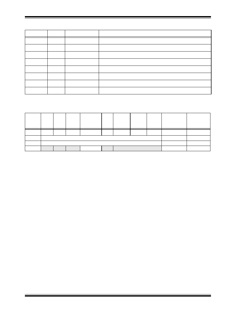
PIC18CXX2
DS39026B-page 86
Preliminary
©
7/99 Microchip Technology Inc.
TABLE 8-7:
PORTD FUNCTIONS
TABLE 8-8:
SUMMARY OF REGISTERS ASSOCIATED WITH PORTD
Name
Bit#
Buffer Type
Function
RD0/PSP0
bit0
ST/TTL
(1)
Input/output port pin or parallel slave port bit0
RD1/PSP1
bit1
ST/TTL
(1)
Input/output port pin or parallel slave port bit1
RD2/PSP2
bit2
ST/TTL
(1)
Input/output port pin or parallel slave port bit2
RD3/PSP3
bit3
ST/TTL
(1)
Input/output port pin or parallel slave port bit3
RD4/PSP4
bit4
ST/TTL
(1)
Input/output port pin or parallel slave port bit4
RD5/PSP5
bit5
ST/TTL
(1)
Input/output port pin or parallel slave port bit5
RD6/PSP6
bit6
ST/TTL
(1)
Input/output port pin or parallel slave port bit6
RD7/PSP7
bit7
ST/TTL
(1)
Input/output port pin or parallel slave port bit7
Legend: ST = Schmitt Trigger input, TTL = TTL input
Note 1: Input buffers are Schmitt Triggers when in I/O mode and TTL buffer when in Parallel Slave Port Mode.
Name
Bit 7
Bit 6
Bit 5
Bit 4
Bit 3
Bit 2
Bit 1
Bit 0
Value on
POR,
BOR
Value on all
other resets
PORTD
RD7
RD6
RD5
RD4
RD3
RD2
RD1
RD0
xxxx xxxx
uuuu uuuu
LATD
LATD Data Output Register
xxxx xxxx
uuuu uuuu
TRISD
PORTD Data Direction Register
1111 1111
1111 1111
TRISE
IBF
OBF
IBOV
PSPMODE
--
PORTE Data Direction Bits
0000 -111
0000 -111
Legend: x = unknown, u = unchanged,
-
= unimplemented read as '0'. Shaded cells are not used by PORTD.
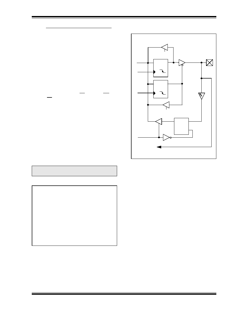
PIC18CXX2
©
7/99 Microchip Technology Inc.
Preliminary
DS39026B-page 87
8.5
PORTE, TRISE and LATE Registers
This section is only applicable to the PIC18C4X2
devices.
PORTE is an 3 bit wide bi-directional port. The corre-
sponding Data Direction Register is TRISE. Setting a
TRISE bit (=1) will make the corresponding PORTE pin
an input, (i.e., put the corresponding output driver in a
hi-impedance mode). Clearing a TRISE bit (=0) will
make the corresponding PORTE pin an output, (i.e.,
put the contents of the output latch on the selected pin).
The Data Latch Register (LATE) is also memory
mapped. Read-modify-write operations on the LATE
register reads and writes the latched output value for
PORTE.
PORTE has three pins RE0/RD/AN5, RE1/WR/AN6
and RE2/CS/AN7, which are individually configurable
as inputs or outputs. These pins have Schmitt Trigger
input buffers.
Figure 8-1 shows the TRISE register, which also con-
trols the parallel slave port operation. Capture2 input/
Compare2 output/PWM output when CCP2MX config-
uration bit is enabled.
PORTE pins are multiplexed with analog inputs. When
selected as an analog input, these pins will read as '0's.
TRISE controls the direction of the RE pins, even when
they are being used as analog inputs. The user must
make sure to keep the pins configured as inputs when
using them as analog inputs.
EXAMPLE 8-5:
INITIALIZING PORTE
FIGURE 8-9:
PORTE BLOCK DIAGRAM
IN I/O PORT MODE
Note:
On a Power-on Reset, these pins are con-
figured as analog inputs.
CLRF PORTE
; Initialize PORTE by
; clearing output
; data latches
CLRF LATE
; Alternate method
; to clear output
; data latches
MOVLW 0x07
; Configure A/D
MOVWF ADCON1
; for digital inputs
MOVLW 0x03
; Value used to
; initialize data
; direction
MOVWF TRISC
; Set RE<0> as inputs
; RE<1> as outputs
; RE<2> as inputs
Data
Bus
WR LATE
WR TRISE
RD PORTE
Data Latch
TRIS Latch
RD TRISE
Schmitt
Trigger
input
buffer
Q
D
CK
Q
D
CK
EN
Q
D
EN
I/O pin
(1)
Note 1: I/O pins have protection diodes to V
DD
and V
SS
.
RD LATE
or
PORTE
To Analog Converter

PIC18CXX2
DS39026B-page 88
Preliminary
©
7/99 Microchip Technology Inc.
Register 8-1:
TRISE Register
R-0
R-0
R/W-0
R/W-0
U-0
R/W-1
R/W-1
R/W-1
IBF
OBF
IBOV
PSPMODE
--
TRISE2
TRISE1
TRISE0
bit 7
bit 0
bit 7
IBF: Input Buffer Full Status bit
1
= A word has been received and waiting to be read by the CPU
0
= No word has been received
bit 6
OBF: Output Buffer Full Status bit
1
= The output buffer still holds a previously written word
0
= The output buffer has been read
bit 5
IBOV: Input Buffer Overflow Detect bit (in microprocessor mode)
1
= A write occurred when a previously input word has not been read
(must be cleared in software)
0
= No overflow occurred
bit 4
PSPMODE: Parallel Slave Port Mode Select bit
1
= Parallel slave port mode
0
= General purpose I/O mode
bit 3
Unimplemented: Read as '0'
bit 2
TRISE2: RE2 direction control bit
1
= Input
0
= Output
bit 1
TRISE1: RE1 direction control bit
1
= Input
0
= Output
bit 0
TRISE0: RE0 direction control bit
1
= Input
0
= Output
Legend:
R = Readable bit
W = Writable bit
U = Unimplemented bit, read as `0'
- n = Value at POR reset
PIC18CXX2
©
7/99 Microchip Technology Inc.
Preliminary
DS39026B-page 89
TABLE 8-9:
PORTE FUNCTIONS
TABLE 8-10:
SUMMARY OF REGISTERS ASSOCIATED WITH PORTE
Name
Bit#
Buffer Type
Function
RE0/RD/AN5
bit0
ST/TTL
(1)
Input/output port pin or read control input in parallel slave port mode
or analog input:
RD
1
= Not a read operation
0
= Read operation. Reads PORTD register (if chip selected)
RE1/WR/AN6
bit1
ST/TTL
(1)
Input/output port pin or write control input in parallel slave port mode
or analog input:
WR
1
= Not a write operation
0
= Write operation. Writes PORTD register (if chip selected)
RE2/CS/AN7
bit2
ST/TTL
(1)
Input/output port pin or chip select control input in parallel slave port
mode or analog input:
CS
1
= Device is not selected
0
= Device is selected
Legend: ST = Schmitt Trigger input, TTL = TTL input
Note 1: Input buffers are Schmitt Triggers when in I/O mode and TTL buffers when in Parallel Slave Port Mode.
Name
Bit 7
Bit 6
Bit 5
Bit 4
Bit 3
Bit 2
Bit 1
Bit 0
Value on
POR,
BOR
Value on all
other
resets
PORTE
--
--
--
--
--
RE2
RE1
RE0
---- -000
---- -000
LATE
--
--
--
--
--
LATE Data Output Register
---- -xxx
---- -uuu
TRISE
IBF
OBF
IBOV
PSPMODE
--
PORTE Data Direction Bits
0000 -111
0000 -111
ADCON1
ADFM
ADCS2
--
--
PCFG3
PCFG2
PCFG1
PCFG0
--0- -000
--0- -000
Legend: x = unknown, u = unchanged,
-
= unimplemented read as '0'. Shaded cells are not used by PORTE.
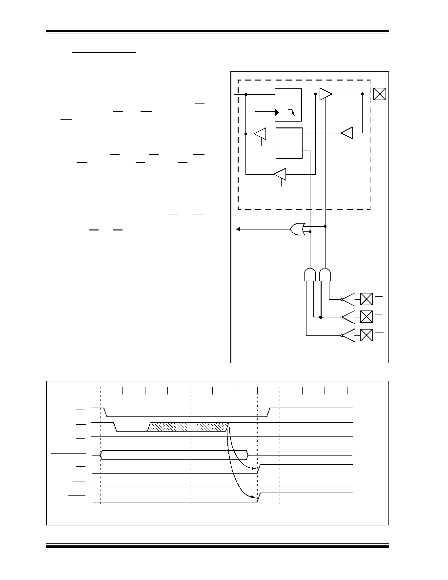
PIC18CXX2
DS39026B-page 90
Preliminary
©
7/99 Microchip Technology Inc.
8.6
Parallel Slave Port
The Parallel Slave Port is implemented on the 40-pin
devices only (PIC18C4X2).
PORTD operates as an 8-bit wide Parallel Slave Port,
or microprocessor port when control bit PSPMODE
(TRISE<4>) is set. In slave mode it is asynchronously
readable and writable by the external world through RD
control input pin RE0/RD and WR control input pin
RE1/WR.
It can directly interface to an 8-bit microprocessor data
bus. The external microprocessor can read or write the
PORTD latch as an 8-bit latch. Setting bit PSPMODE
enables port pin RE0/RD to be the RD input, RE1/WR
to be the WR input and RE2/CS to be the CS (chip
select) input. For this functionality, the corresponding
data direction bits of the TRISE register (TRISE<2:0>)
must be configured as inputs (set). The A/D port con-
figuration bits PCFG2:PCFG0 (ADCON1<2:0>) must
be set, which will configure pins RE2:RE0 as digital I/O.
A write to the PSP occurs when both the CS and WR
lines are first detected low. A read from the PSP occurs
when both the CS and RD lines are first detected low.
The PORTE I/O pins become control inputs for the
microprocessor port when bit PSPMODE (TRISE<4>)
is set. In this mode, the user must make sure that the
TRISE<2:0> bits are set (pins are configured as digital
inputs), and the ADCON1 is configured for digital I/O. In
this mode, the input buffers are TTL.
FIGURE 8-10: PORTD AND PORTE BLOCK
DIAGRAM
(PARALLEL SLAVE PORT)
FIGURE 8-11: PARALLEL SLAVE PORT WRITE WAVEFORMS
Data Bus
WR LATD
RDx
Q
D
CK
EN
Q
D
EN
RD PORTD
Pin
One bit of PORTD
Set Interrupt Flag
PSPIF (PIR1<7>)
Read
Chip Select
Write
RD
CS
WR
Note: I/O pin has protection diodes to V
DD
and V
SS
.
TTL
TTL
TTL
TTL
or
PORTD
RD LATD
Data Latch
Q1
Q2
Q3
Q4
CS
Q1
Q2
Q3
Q4
Q1
Q2
Q3
Q4
WR
RD
IBF
OBF
PSPIF
PORTD<7:0>
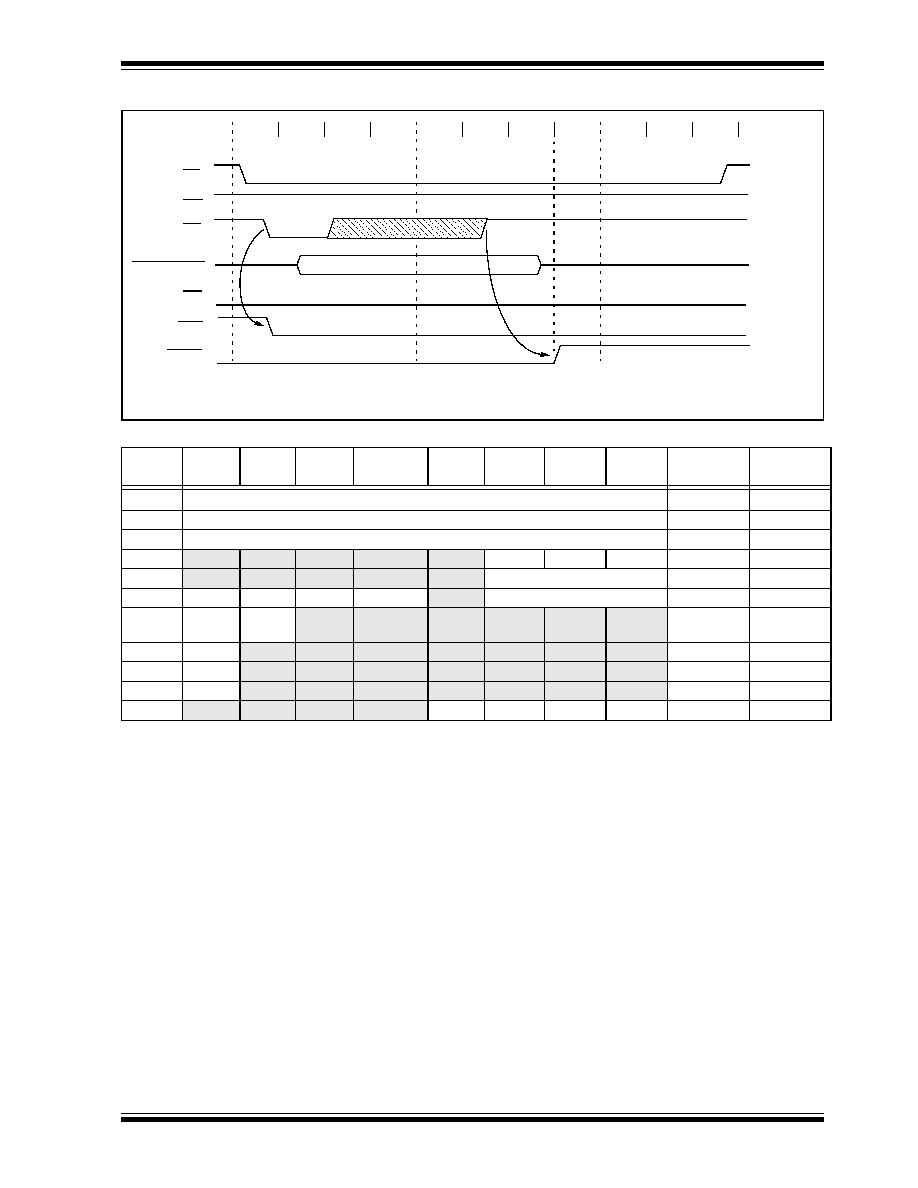
PIC18CXX2
©
7/99 Microchip Technology Inc.
Preliminary
DS39026B-page 91
FIGURE 8-12: PARALLEL SLAVE PORT READ WAVEFORMS
TABLE 8-11:
REGISTERS ASSOCIATED WITH PARALLEL SLAVE PORT
Name
Bit 7
Bit 6
Bit 5
Bit 4
Bit 3
Bit 2
Bit 1
Bit 0
Value on
POR, BOR
Value on all
other resets
PORTD
Port data latch when written; port pins when read
xxxx xxxx
uuuu uuuu
LATD
LATD Data Output Bits
xxxx xxxx
uuuu uuuu
TRISD
PORTD Data Direction Bits
1111 1111
1111 1111
PORTE
--
--
--
--
--
RE2
RE1
RE0
---- -000
---- -000
LATE
--
--
--
--
--
LATE Data Output Bits
---- -xxx
---- -uuu
TRISE
IBF
OBF
IBOV
PSPMODE
--
PORTE Data Direction Bits
0000 -111
0000 -111
INTCON
GIE/
GIEH
PEIE/
GIEL
TMR0IF
INT0IE
RBIE
TMR0IF
INT0IF
RBIF
0000 000x
0000 000u
PIR1
PSPIF
ADIF
RCIF
TXIF
SSPIF
CCP1IF
TMR2IF
TMR1IF
0000 0000
0000 0000
PIE1
PSPIE
ADIE
RCIE
TXIE
SSPIE
CCP1IE
TMR2IE
TMR1IE
0000 0000
0000 0000
IPR1
PSPIP
ADIP
RCIP
TXIP
SSPIP
CCP1IP
TMR2IP
TMR1IP
0000 0000
0000 0000
ADCON1
ADFM
ADCS2
--
--
PCFG3
PCFG2
PCFG1
PCFG0
--0- -000
--0- -000
Legend: x = unknown, u = unchanged,
-
= unimplemented read as '0'.
Shaded cells are not used by the Parallel Slave Port.
Q1
Q2
Q3
Q4
CS
Q1
Q2
Q3
Q4
Q1
Q2
Q3
Q4
WR
IBF
PSPIF
RD
OBF
PORTD<7:0>

PIC18CXX2
DS39026B-page 92
Preliminary
©
7/99 Microchip Technology Inc.
NOTES:
PIC18CXX2
©
7/99 Microchip Technology Inc.
Preliminary
DS39026B-page 93
9.0
TIMER0 MODULE
The Timer0 module has the following features:
∑ Software selectable as an 8-bit or 16-bit timer/
counter
∑ Readable and writable
∑ Dedicated 8-bit software programmable prescaler
∑ Clock source selectable to be external or internal
∑ Interrupt on overflow from FFh to 00h in 8-bit
mode and FFFFh to 0000h in 16-bit mode
∑ Edge select for external clock
Figure 9-1 shows a simplified block diagram of the
Timer0 module in 8-bit mode and Figure 9-1 shows a
simplified block diagram of the Timer0 module in 16-bit
mode.
The T0CON register is a readable and writable register
that controls all the aspects of Timer0, including the
prescale selection.
Register 9-1:
T0CON: Timer0 Control Register
R/W-1
R/W-1
R/W-1
R/W-1
R/W-1
R/W-1
R/W-1
R/W-1
TMR0ON
T08BIT
T0CS
T0SE
PSA
T0PS2
T0PS1
T0PS0
bit 7
bit 0
bit 7
TMR0ON: Timer0 On/Off Control bit
1
= Enables Timer0
0
= Stops Timer0
bit 6
T08BIT: Timer0 8-bit/16-bit Control bit
1
= Timer0 is configured as an 8-bit timer/counter
0
= Timer0 is configured as a 16-bit timer/counter
bit 5
T0CS: Timer0 Clock Source Select bit
1
= Transition on T0CKI pin
0
= Internal instruction cycle clock (CLKOUT)
bit 4
T0SE: Timer0 Source Edge Select bit
1
= Increment on high-to-low transition on T0CKI pin
0
= Increment on low-to-high transition on T0CKI pin
bit 3
PSA: Timer0 Prescaler Assignment bit
1
= TImer0 prescaler is NOT assigned. Timer0 clock input bypasses prescaler
0
= Timer0 prescaler is assigned. Timer0 clock input comes from prescaler output
bit 2:0
T0PS2:T0PS0: Timer0 Prescaler Select bits
111
= 1:256 prescale value
110
= 1:128 prescale value
101
= 1:64 prescale value
100
= 1:32 prescale value
011
= 1:16 prescale value
010
= 1:8 prescale value
001
= 1:4 prescale value
000
= 1:2 prescale value
Legend:
R = Readable bit
W = Writable bit
U = Unimplemented bit, read as `0'
- n = Value at POR reset
'1' = Bit is set
'0' = Bit is cleared
x = Bit is unknown
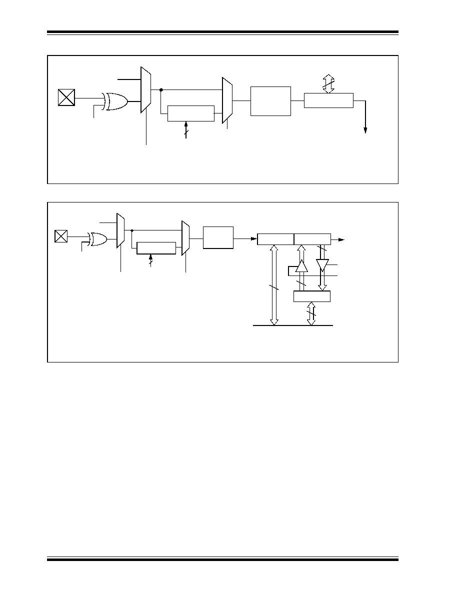
PIC18CXX2
DS39026B-page 94
Preliminary
©
7/99 Microchip Technology Inc.
FIGURE 9-1:
TIMER0 BLOCK DIAGRAM IN 8-BIT MODE
FIGURE 9-2:
TIMER0 BLOCK DIAGRAM IN 16-BIT MODE
Note:
Upon reset, Timer0 is enabled in 8-bit mode with clock input from T0CKI max. prescale.
RA4/T0CKI
T0SE
0
1
0
1
Pin
T0CS
F
OSC
/4
Programmable
Prescaler
Sync with
Internal
clocks
TMR0
(2 Tcy delay)
Data Bus
8
PSA
T0PS2, T0PS1, T0PS0
Set Interrupt
Flag bit TMR0IF
on overflow
3
Note:
Upon reset, Timer0 is enabled in 8-bit mode with clock input from T0CKI max. prescale.
T0CKI pin
T0SE
0
1
0
1
T0CS
F
OSC
/4
Programmable
Prescaler
Sync with
Internal
Clocks
TMR0L
(2 Tcy delay)
Data Bus<7:0>
8
PSA
T0PS2, T0PS1, T0PS0
Set Interrupt
Flag bit TMR0IF
on overflow
3
TMR0
TMR0H
High Byte
8
8
8
Read TMR0L
Write TMR0L
PIC18CXX2
©
7/99 Microchip Technology Inc.
Preliminary
DS39026B-page 95
9.1
Timer0 Operation
Timer0 can operate as a timer or as a counter.
Timer mode is selected by clearing the T0CS bit. In
timer mode, the Timer0 module will increment every
instruction cycle (without prescaler). If the TMR0 regis-
ter is written, the increment is inhibited for the following
two instruction cycles. The user can work around this
by writing an adjusted value to the TMR0 register.
Counter mode is selected by setting the T0CS bit. In
counter mode, Timer0 will increment either on every
rising or falling edge of pin RA4/T0CKI. The increment-
ing edge is determined by the Timer0 Source Edge
Select bit (T0SE). Clearing the T0SE bit selects the ris-
ing edge. Restrictions on the external clock input are
discussed below.
When an external clock input is used for Timer0, it must
meet certain requirements. The requirements ensure
the external clock can be synchronized with the internal
phase clock (T
OSC
). Also, there is a delay in the actual
incrementing of Timer0 after synchronization.
9.2
Prescaler
An 8-bit counter is available as a prescaler for the
Timer0 module. The prescaler is not readable or writ-
able.
The PSA and T0PS2:T0PS0 bits determine the pres-
caler assignment and prescale ratio.
Clearing bit PSA will assign the prescaler to the Timer0
module. When the prescaler is assigned to the Timer0
module, prescale values of 1:2, 1:4, ..., 1:256 are
selectable.
When assigned to the Timer0 module, all instructions
writing to the TMR0 register (e.g.
CLRF TMR0,
MOVWF TMR0, BSF TMR0, x
....etc.) will clear the
prescaler count.
9.2.1
SWITCHING PRESCALER ASSIGNMENT
The prescaler assignment is fully under software con-
trol, (i.e., it can be changed "on-the-fly" during program
execution).
9.3
Timer0 Interrupt
The TMR0 interrupt is generated when the TMR0 reg-
ister overflows from FFh to 00h in 8-bit mode or FFFFh
to 0000h in 16-bit mode. This overflow sets the TMR0IF
bit. The interrupt can be masked by clearing the
TMR0IE bit. The TMR0IE bit must be cleared in soft-
ware by the Timer0 module interrupt service routine
before re-enabling this interrupt. The TMR0 interrupt
cannot awaken the processor from SLEEP, since the
timer is shut off during SLEEP.
9.4
16-Bit Mode Timer Reads and Writes
TMR0H is not the high byte of the timer/counter in 16-
bit mode, but is actually a buffered version of the high
byte of Timer0 (refer to Figure 9-1). The high byte of
the Timer0 counter/timer is not directly readable nor
writable. TMR0H is updated with the contents of the
high byte of Timer0 during a read of TMR0L. This pro-
vides the ability to read all 16-bits of Timer0 without
having to verify that the read of the high and low byte
were valid due to a rollover between successive reads
of the high and low byte.
A write to the high byte of Timer0 must also take place
through the TMR0H buffer register. Timer0 high byte is
updated with the contents of TMR0H when a write
occurs to TMR0L. This allows all 16 bits of Timer0 to
be updated at once.
TABLE 9-1:
REGISTERS ASSOCIATED WITH TIMER0
Note:
Writing to TMR0 when the prescaler is
assigned to Timer0 will clear the prescaler
count, but will not change the prescaler
assignment.
Name
Bit 7
Bit 6
Bit 5
Bit 4
Bit 3
Bit 2
Bit 1
Bit 0
Value on
POR, BOR
Value on all
other resets
TMR0L
Timer0 Module's Low Byte Register
xxxx xxxx
uuuu uuuu
TMR0H
Timer0 Module's High Byte Register
0000 0000
0000 0000
INTCON
GIE/GIEH
PEIE/GIEL TMR0IE INT0IE
RBIE
TMR0IF INT0IF
RBIF
0000 000x
0000 000u
T0CON
TMR0ON
T08BIT
T0CS
T0SE
PSA
T0PS2
T0PS1
T0PS0
1111 1111
1111 1111
TRISA
--
--
PORTA Data Direction Register
--11 1111
--11 1111
Legend: x = unknown, u = unchanged,
-
= unimplemented locations read as '0'.
Shaded cells are not used by Timer0.

PIC18CXX2
DS39026B-page 96
Preliminary
©
7/99 Microchip Technology Inc.
NOTES:

PIC18CXX2
©
7/99 Microchip Technology Inc.
Preliminary
DS39026B-page 97
10.0
TIMER1 MODULE
The Timer1 module timer/counter has the following fea-
tures:
∑ 16-bit timer/counter
(Two 8-bit registers; TMR1H and TMR1L)
∑ Readable and writable (Both registers)
∑ Internal or external clock select
∑ Interrupt on overflow from FFFFh to 0000h
∑ Reset from CCP module special event trigger
Figure 10-1 is a simplified block diagram of the Timer1
module.
Register 10-1 shows the Timer1 control register. This
register controls the operating mode of the Timer1
module as well as contains the Timer1 oscillator enable
bit (T1OSCEN). Timer1 can be enabled/disabled by
setting/clearing control bit TMR1ON (T1CON<0>).
Register 10-1: T1CON: Timer1 Control Register
R/W-0
U-0
R/W-0
R/W-0
R/W-0
R/W-0
R/W-0
R/W-0
RD16
--
T1CKPS1
T1CKPS0
T1OSCEN
T1SYNC
TMR1CS
TMR1ON
bit 7
bit 0
bit 7
RD16: 16-bit Read/Write Mode Enable bit
1
= Enables register Read/Write of TImer1 in one 16-bit operation
0
= Enables register Read/Write of Timer1 in two 8-bit operations
bit 6
Unimplemented: Read as '0'
bit 5:4
T1CKPS1:T1CKPS0: Timer1 Input Clock Prescale Select bits
11
= 1:8 Prescale value
10
= 1:4 Prescale value
01
= 1:2 Prescale value
00
= 1:1 Prescale value
bit 3
T1OSCEN: Timer1 Oscillator Enable bit
1
= Timer1 Oscillator is enabled
0
= Timer1 Oscillator is shut off.
The oscillator inverter and feedback resistor are turned off to eliminate power drain
bit 2
T1SYNC: Timer1 External Clock Input Synchronization Select bit
When TMR1CS = 1:
1
= Do not synchronize external clock input
0
= Synchronize external clock input
When TMR1CS = 0:
This bit is ignored. Timer1 uses the internal clock when TMR1CS = 0.
bit 1
TMR1CS: Timer1 Clock Source Select bit
1
= External clock from pin RC0/T1OSO/T13CKI (on the rising edge)
0
= Internal clock (F
OSC
/4)
bit 0
TMR1ON: Timer1 On bit
1
= Enables Timer1
0
= Stops Timer1
Legend:
R = Readable bit
W = Writable bit
U = Unimplemented bit, read as `0'
- n = Value at POR reset
'1' = Bit is set
'0' = Bit is cleared
x = Bit is unknown
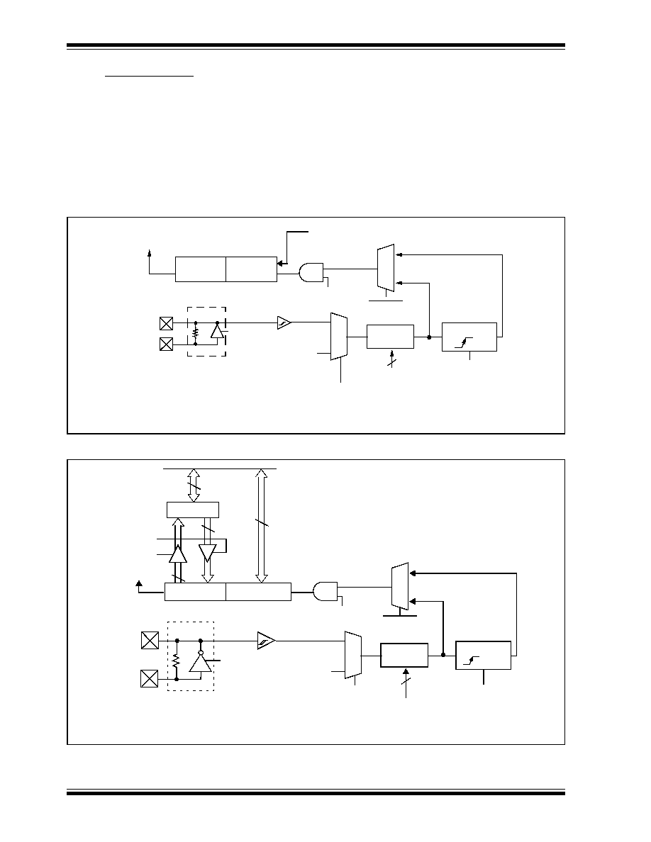
PIC18CXX2
DS39026B-page 98
Preliminary
©
7/99 Microchip Technology Inc.
10.1
Timer1 Operation
Timer1 can operate in one of these modes:
∑ As a timer
∑ As a synchronous counter
∑ As an asynchronous counter
The operating mode is determined by the clock select
bit, TMR1CS (T1CON<1>).
When TMR1CS = 0, Timer1 increments every instruc-
tion cycle. When TMR1CS = 1, Timer1 increments on
every rising edge of the external clock input or the
Timer1 oscillator, if enabled.
When the Timer1 oscillator is enabled (T1OSCEN is
set), the RC1/T1OSI and RC0/T1OSO/T1CKI pins
become inputs. That is, the TRISC<1:0> value is
ignored.
Timer1 also has an internal "reset input". This reset can
be generated by the CCP module (Section 13.0).
FIGURE 10-1: TIMER1 BLOCK DIAGRAM
FIGURE 10-2: TIMER1 BLOCK DIAGRAM: 16-BIT READ/WRITE MODE
TMR1H
TMR1L
T1SYNC
TMR1CS
T1CKPS1:T1CKPS0
SLEEP input
F
OSC
/4
Internal
Clock
TMR1ON
on/off
Prescaler
1, 2, 4, 8
Synchronize
det
1
0
0
1
Synchronized
Clock Input
2
TMR1IF
Overflow
TMR1
CLR
CCP Special Event Trigger
T1OSCEN
Enable
Oscillator
(1)
T1OSC
Interrupt
Flag Bit
Note 1: When enable bit T1OSCEN is cleared, the inverter and feedback resistor are turned off. This
eliminates power drain.
T1OSI
T1CKI/T1OSO
Timer 1
TMR1L
T1OSC
T1SYNC
TMR1CS
T1CKPS1:T1CKPS0
SLEEP input
T1OSCEN
Enable
Oscillator
(1)
TMR1IF
Overflow
Interrupt
Fosc/4
Internal
Clock
TMR1ON
on/off
Prescaler
1, 2, 4, 8
Synchronize
det
1
0
0
1
Synchronized
clock input
2
T13CKI/T1OSO
T1OSI
TMR1
flag bit
Note 1: When enable bit T1OSCEN is cleared, the inverter and feedback resistor are turned off. This eliminates
power drain.
high byte
Data bus<7:0>
8
TMR1H
8
8
8
Read TMR1L
Write TMR1L

PIC18CXX2
©
7/99 Microchip Technology Inc.
Preliminary
DS39026B-page 99
10.2
Timer1 Oscillator
A crystal oscillator circuit is built-in between pins T1OSI
(input) and T1OSO (amplifier output). It is enabled by
setting control bit T1OSCEN (T1CON<3>). The oscilla-
tor is a low power oscillator rated up to 200 kHz. It will
continue to run during SLEEP. It is primarily intended
for a 32 kHz crystal. Table 10-1 shows the capacitor
selection for the Timer1 oscillator.
The user must provide a software time delay to ensure
proper start-up of the Timer1 oscillator.
10.3
Timer1 Interrupt
The TMR1 Register pair (TMR1H:TMR1L) increments
from 0000h to FFFFh and rolls over to 0000h. The
TMR1 Interrupt, if enabled, is generated on overflow,
which is latched in interrupt flag bit TMR1IF (PIR1<0>).
This interrupt can be enabled/disabled by setting/clear-
ing TMR1 interrupt enable bit TMR1IE (PIE1<0>).
10.4
Resetting Timer1 using a CCP Trigger
Output
If the CCP module is configured in compare mode to
generate a "special event trigger" (CCP1M3:CCP1M0
= 1011), this signal will reset Timer1 and start an A/D
conversion (if the A/D module is enabled).
Timer1 must be configured for either timer or synchro-
nized counter mode to take advantage of this feature. If
Timer1 is running in asynchronous counter mode, this
reset operation may not work.
In the event that a write to Timer1 coincides with a spe-
cial event trigger from CCP1, the write will take prece-
dence.
In this mode of operation, the CCPR1H:CCPR1L regis-
ters pair effectively becomes the period register for
Timer1.
10.5
Timer1 16-Bit Read/Write Mode
Timer1 can be configured for 16-bit reads and writes
(see Figure 10-2). When the RD16 control bit
(T1CON<7>) is set, the address for TMR1H is mapped
to a buffer register for the high byte of Timer1. A read
from TMR1L will load the contents of the high byte of
Timer1 into the Timer1 high byte buffer. This provides
the user with the ability to accurately read all 16-bits of
Timer1 without having to determine whether a read of
the high byte followed by a read of the low byte is valid
due to a rollover between reads.
A write to the high byte of Timer1 must also take place
through the TMR1H buffer register. Timer1 high byte is
updated with the contents of TMR1H when a write
occurs to TMR1L. This allows a user to write all 16 bits
to both the high and low bytes of Timer1 at once.
The high byte of Timer1 is not directly readable or writ-
able in this mode. All reads and writes must take place
through the Timer1 high byte buffer register. Writes to
TMR1H do not clear the Timer1 prescaler. The pres-
caler is only cleared on writes to TMR1L.
TABLE 10-1: CAPACITOR SELECTION FOR
THE ALTERNATE OSCILLATOR
Osc Type
Freq
C1
C2
LP
32 kHz
TBD
(1)
TBD
(1)
Crystal to be Tested:
32.768 kHz
Epson C-001R32.768K-A
±
20
PPM
Note 1: Microchip suggests 33 pF as a starting
point in validating the oscillator circuit.
2: Higher capacitance increases the stability
of the oscillator, but also increases the
start-up time.
3: Since each resonator/crystal has its own
characteristics, the user should consult the
resonator/crystal manufacturer for appro-
priate values of external components.
4: Capacitor values are for design guidance
only.
Note:
The special event triggers from the CCP1
module will not set interrupt flag bit
TMR1IF (PIR1<0>).
PIC18CXX2
DS39026B-page 100
Preliminary
©
7/99 Microchip Technology Inc.
TABLE 10-2:
REGISTERS ASSOCIATED WITH TIMER1 AS A TIMER/COUNTER
Name
Bit 7
Bit 6
Bit 5
Bit 4
Bit 3
Bit 2
Bit 1
Bit 0
Value on
POR,
BOR
Value on
all other
resets
INTCON
GIE/
GIEH
PEIE/
GIEL
TMR0IE
INT0IE
RBIE
TMR0IF
INT0IF
RBIF
0000 000x
0000 000u
PIR1
PSPIF
(1)
ADIF
RCIF
TXIF
SSPIF
CCP1IF
TMR2IF
TMR1IF
0000 0000
0000 0000
PIE1
PSPIE
(1)
ADIE
RCIE
TXIE
SSPIE
CCP1IE
TMR2IE
TMR1IE
0000 0000
0000 0000
IPR1
PSPIP
(1)
ADIP
RCIP
TXIP
SSPIP
CCP1IP
TMR2IP
TMR1IP
0000 0000
0000 0000
TMR1L
Holding register for the Least Significant Byte of the 16-bit TMR1 register
xxxx xxxx
uuuu uuuu
TMR1H
Holding register for the Most Significant Byte of the 16-bit TMR1 register
xxxx xxxx
uuuu uuuu
T1CON
--
--
T1CKPS1
T1CKPS0
T1OSCEN
T1SYNC
TMR1CS
TMR1ON
--00 0000
--uu uuuu
Legend: x = unknown, u = unchanged,
-
= unimplemented read as '0'.
Shaded cells are not used by the Timer1 module.
Note 1: The PSPIF, PSPIE and PSPIP bits are reserved on the PIC18C2X2 devices. Always maintain these bits clear.

PIC18CXX2
©
7/99 Microchip Technology Inc.
Preliminary
DS39026B-page 101
NOTES:

PIC18CXX2
DS39026B-page 102
Preliminary
©
7/99 Microchip Technology Inc.
11.0
TIMER2 MODULE
The Timer2 module timer has the following features:
∑ 8-bit timer (TMR2 register)
∑ 8-bit period register (PR2)
∑ Readable and writable (both registers)
∑ Software programmable prescaler (1:1, 1:4, 1:16)
∑ Software programmable postscaler (1:1 to 1:16)
∑ Interrupt on TMR2 match of PR2
∑ SSP module optional use of TMR2 output to gen-
erate clock shift
Timer2 has a control register shown in Register 11-1.
Timer2 can be shut off by clearing control bit TMR2ON
(T2CON<2>) to minimize power consumption.
Figure 11-1 is a simplified block diagram of the Timer2
module. Figure 11-1 shows the Timer2 control register.
The prescaler and postscaler selection of Timer2 are
controlled by this register.
11.1
Timer2 Operation
Timer2 can be used as the PWM time-base for the
PWM mode of the CCP module. The TMR2 register is
readable and writable, and is cleared on any device
reset. The input clock (F
OSC
/4) has a prescale option of
1:1, 1:4 or 1:16, selected by control bits
T2CKPS1:T2CKPS0 (T2CON<1:0>). The match out-
put of TMR2 goes through a 4-bit postscaler (which
gives a 1:1 to 1:16 scaling inclusive) to generate a
TMR2 interrupt (latched in flag bit TMR2IF, (PIR1<1>)).
The prescaler and postscaler counters are cleared
when any of the following occurs:
∑ a write to the TMR2 register
∑ a write to the T2CON register
∑ any device reset (Power-on Reset, MCLR reset,
Watchdog Timer reset, or Brown-out Reset)
TMR2 is not cleared when T2CON is written.
Register 11-1: T2CON: Timer2 Control Register
U-0
R/W-0
R/W-0
R/W-0
R/W-0
R/W-0
R/W-0
R/W-0
--
TOUTPS3
TOUTPS2
TOUTPS1
TOUTPS0
TMR2ON
T2CKPS1
T2CKPS0
bit
7
bit 0
bit 7
Unimplemented: Read as '0'
bit 6:3
TOUTPS3:TOUTPS0: Timer2 Output Postscale Select bits
0000
= 1:1 Postscale
0001
= 1:2 Postscale
∑
∑
∑
1111
= 1:16 Postscale
bit 2
TMR2ON: Timer2 On bit
1
= Timer2 is on
0
= Timer2 is off
bit 1:0
T2CKPS1:T2CKPS0: Timer2 Clock Prescale Select bits
00
= Prescaler is 1
01
= Prescaler is 4
1x
= Prescaler is 16
Legend:
R = Readable bit
W = Writable bit
U = Unimplemented bit, read as `0'
- n = Value at POR reset
'1' = Bit is set
'0' = Bit is cleared
x = Bit is unknown
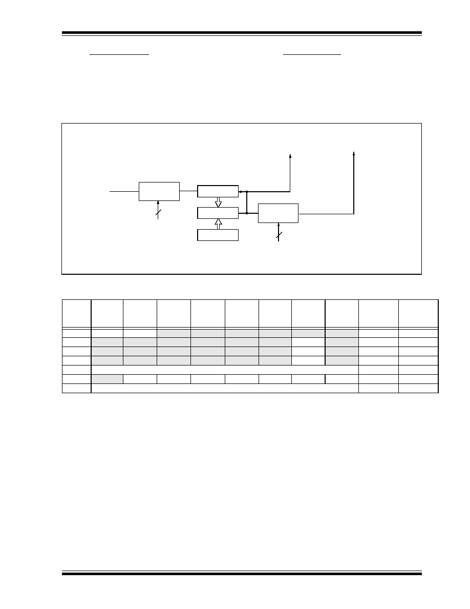
PIC18CXX2
©
7/99 Microchip Technology Inc.
Preliminary
DS39026B-page 103
11.2
Timer2 Interrupt
The Timer2 module has an 8-bit period register PR2.
Timer2 increments from 00h until it matches PR2 and
then resets to 00h on the next increment cycle. PR2 is
a readable and writable register. The PR2 register is ini-
tialized to FFh upon reset.
11.3
Output of TMR2
The output of TMR2 (before the postscaler) is fed to the
Synchronous Serial Port module, which optionally uses
it to generate the shift clock.
FIGURE 11-1: TIMER2 BLOCK DIAGRAM
TABLE 11-1:
REGISTERS ASSOCIATED WITH TIMER2 AS A TIMER/COUNTER
Comparator
TMR2
Sets flag
TMR2
output
(1)
Reset
Postscaler
Prescaler
PR2
2
F
OSC
/4
1:1
1:16
1:1, 1:4, 1:16
EQ
4
bit TMR2IF
Note 1: TMR2 register output can be software selected by the SSP Module as a baud clock.
to
TOUTPS3:TOUTPS0
T2CKPS1:T2CKPS0
Name
Bit 7
Bit 6
Bit 5
Bit 4
Bit 3
Bit 2
Bit 1
Bit 0
Value on
POR, BOR
Value on
all other
resets
INTCON
GIE/GIEH
PEIE/GIEL
TMR0IE
INT0IE
RBIE
TMR0IF
INT0IF
RBIF
0000 000x
0000 000u
PIR1
PSPIF
(1)
ADIF
RCIF
TXIF
SSPIF
CCP1IF
TMR2IF
TMR1IF
0000 0000
0000 0000
PIE1
PSPIE
(1)
ADIE
RCIE
TXIE
SSPIE
CCP1IE
TMR2IE
TMR1IE
0000 0000
0000 0000
IPR1
PSPIP
(1)
ADIP
RCIP
TXIP
SSPIP
CCP1IP
TMR2IP
TMR1IP
0000 0000
0000 0000
TMR2
Timer2 module's register
0000 0000
0000 0000
T2CON
--
TOUTPS3
TOUTPS2
TOUTPS1
TOUTPS0
TMR2ON
T2CKPS1
T2CKPS0
-000 0000
-000 0000
PR2
Timer2 Period Register
1111 1111
1111 1111
Legend:
x = unknown, u = unchanged,
-
= unimplemented read as '0'. Shaded cells are not used by the Timer2 module.
Note 1:
The PSPIF, PSPIE and PSPIP bits are reserved on the PIC18C2X2 devices. Always maintain these bits clear.

PIC18CXX2
DS39026B-page 104
Preliminary
©
7/99 Microchip Technology Inc.
NOTES:

PIC18CXX2
©
7/99 Microchip Technology Inc.
Preliminary
DS39026B-page 105
12.0
TIMER3 MODULE
The Timer3 module timer/counter has the following fea-
tures:
∑ 16-bit timer/counter
(Two 8-bit registers; TMR3H and TMR3L)
∑ Readable and writable (both registers)
∑ Internal or external clock select
∑ Interrupt on overflow from FFFFh to 0000h
∑ Reset from CCP module trigger
Figure 12-1 is a simplified block diagram of the Timer3
module.
Register 12-1 shows the Timer3 control register. This
register controls the operating mode of the Timer3
module and sets the CCP clock source.
Register 10-1 shows the Timer1 control register. This
register controls the operating mode of the Timer1
module, as well as contains the Timer1 oscillator
enable bit (T1OSCEN), which can be a clock source for
Timer3.
Register 12-1: T3CON: Timer3 Control Register
R/W-0
R/W-0
R/W-0
R/W-0
R/W-0
R/W-0
R/W-0
R/W-0
RD16
T3CCP2
T3CKPS1
T3CKPS0
T3CCP1
T3SYNC
TMR3CS
TMR3ON
bit 7
bit 0
bit 7
RD16: 16-bit Read/Write Mode Enable
1
= Enables register Read/Write of Timer3 in one 16-bit operation
0
= Enables register Read/Write of Timer3 in two 8-bit operations
bit 6,3
T3CCP2:T3CCP1: Timer3 and Timer1 to CCPx Enable bits
1x
= Timer3 is the clock source for compare/capture CCP modules
01
= Timer3 is the clock source for compare/capture of CCP2,
Timer1 is the clock source for compare/capture of CCP1
00
= Timer1 is the clock source for compare/capture CCP modules
bit 5:4
T3CKPS1:T3CKPS0: Timer3 Input Clock Prescale Select bits
11
= 1:8 Prescale value
10
= 1:4 Prescale value
01
= 1:2 Prescale value
00
= 1:1 Prescale value
bit 2
T3SYNC: Timer3 External Clock Input Synchronization Control bit
(Not usable if the system clock comes from Timer1/Timer3)
When TMR3CS = 1:
1
= Do not synchronize external clock input
0
= Synchronize external clock input
When TMR3CS = 0:
This bit is ignored. Timer3 uses the internal clock when TMR3CS = 0.
bit 1
TMR3CS: Timer3 Clock Source Select bit
1
= External clock input from Timer1 oscillator or T1CKI (on the rising edge after the first falling
edge)
0
= Internal clock (Fosc/4)
bit 0
TMR3ON: Timer3 On bit
1
= Enables Timer3
0
= Stops Timer3
Legend:
R = Readable bit
W = Writable bit
U = Unimplemented bit, read as `0'
- n = Value at POR reset
'1' = Bit is set
'0' = Bit is cleared
x = Bit is unknown
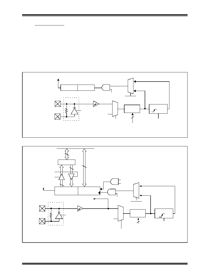
PIC18CXX2
DS39026B-page 106
Preliminary
©
7/99 Microchip Technology Inc.
12.1
Timer3 Operation
Timer3 can operate in one of these modes:
∑ As a timer
∑ As a synchronous counter
∑ As an asynchronous counter
The operating mode is determined by the clock select
bit, TMR3CS (T3CON<1>).
When TMR3CS = 0, Timer3 increments every instruc-
tion cycle. When TMR3CS = 1, Timer3 increments on
every rising edge of the Timer1 external clock input or
the Timer1 oscillator, if enabled.
When the Timer1 oscillator is enabled (T1OSCEN is
set), the RC1/T1OSI and RC0/T1OSO/T1CKI pins
become inputs. That is, the TRISC<1:0> value is
ignored.
Timer3 also has an internal "reset input". This reset can
be generated by the CCP module (Section 12.0).
FIGURE 12-1: TIMER3 BLOCK DIAGRAM
FIGURE 12-2: TIMER3 BLOCK DIAGRAM CONFIGURED IN 16-BIT MODE
TMR3H
TMR3L
T1OSC
T3SYNC
TMR3CS
T3CKPS1:T3CKPS0
SLEEP input
T1OSCEN
Enable
Oscillator
(1)
TMR3IF
Overflow
Interrupt
Fosc/4
Internal
Clock
TMR3ON
on/off
Prescaler
1, 2, 4, 8
Synchronize
det
1
0
0
1
Synchronized
clock input
2
T1OSO/
T1OSI
flag bit
(3)
Note 1: When enable bit T1OSCEN is cleared, the inverter and feedback resistor are turned off. This eliminates power drain.
T13CKI
Timer3
TMR3L
T1OSC
T3SYNC
TMR3CS
T3CKPS1:T3CKPS0
SLEEP input
T1OSCEN
Enable
Oscillator
(1)
F
OSC
/4
Internal
Clock
TMR3ON
on/off
Prescaler
1, 2, 4, 8
Synchronize
det
1
0
0
1
Synchronized
clock input
2
T1OSO/
T1OSI
TMR3
T13CKI
CLR
CCP Special Trigger
T3CCPx
To Timer1 Clock Input
Note 1:
When the T1OSCEN bit is cleared, the inverter and feedback resistor are turned off. This eliminates power drain.
High Byte
Data bus<7:0>
8
TMR3H
8
8
8
Read TMR3L
Write TMR3L
Set TMR3IF flag bit
on overflow
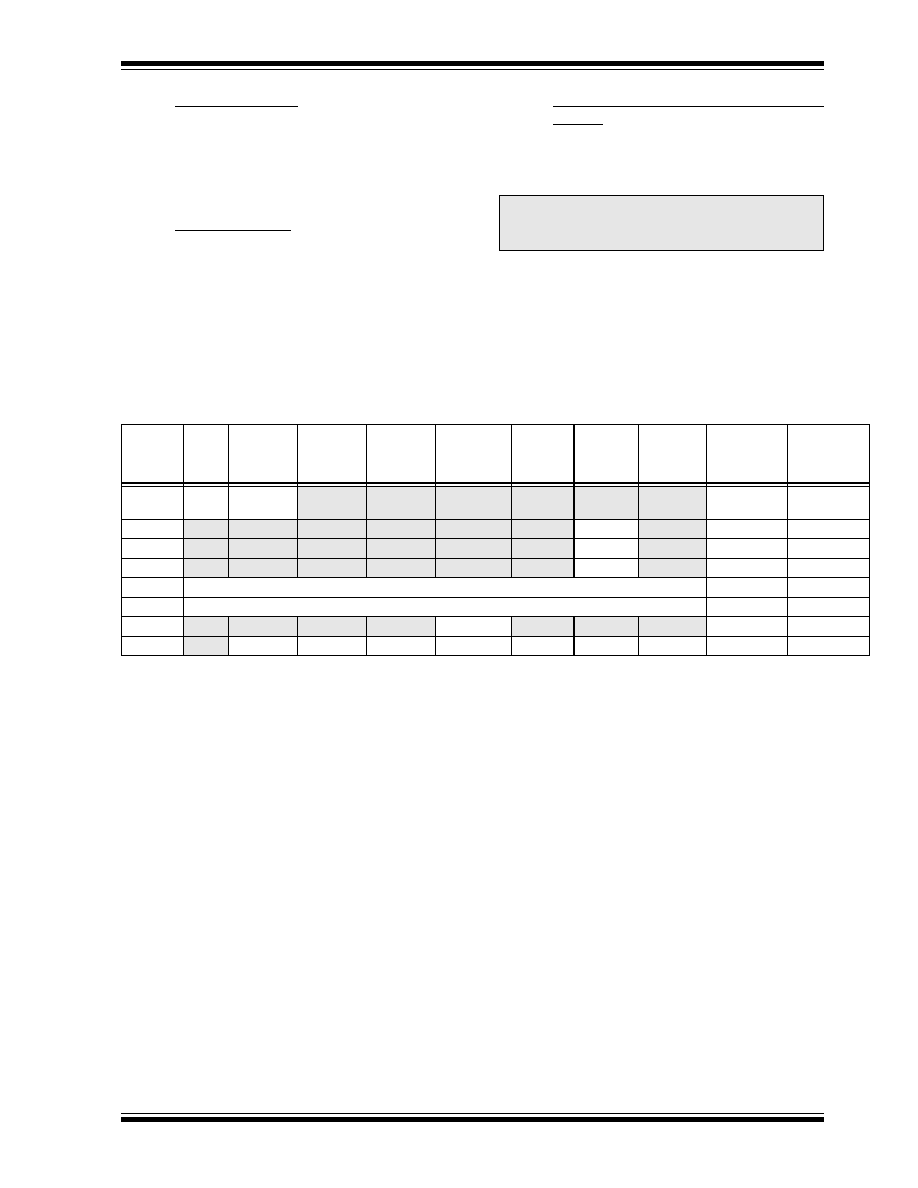
PIC18CXX2
©
7/99 Microchip Technology Inc.
Preliminary
DS39026B-page 107
12.2
Timer1 Oscillator
The Timer1 oscillator may be used as the clock source
for Timer3. The Timer1 oscillator is enabled by setting
the T1OSCEN (T1CON<3>) bit. The oscillator is a low
power oscillator rated up to 200 KHz. See Section 10.0
for further details.
12.3
Timer3 Interrupt
The TMR3 Register pair (TMR3H:TMR3L) increments
from 0000h to FFFFh and rolls over to 0000h. The
TMR3 Interrupt, if enabled, is generated on overflow
which is latched in interrupt flag bit TMR3IF (PIR2<1>).
This interrupt can be enabled/disabled by setting/clear-
ing TMR3 interrupt enable bit TMR3IE (PIE2<1>).
12.4
Resetting Timer3 Using a CCP Trigger
Output
If the CCP module is configured in compare mode to
generate a "special event trigger" (CCP1M3:CCP1M0
= 1011), this signal will reset Timer3.
Timer3 must be configured for either timer or synchro-
nized counter mode to take advantage of this feature. If
Timer3 is running in asynchronous counter mode, this
reset operation may not work. In the event that a write
to Timer3 coincides with a special event trigger from
CCP1, the write will take precedence. In this mode of
operation, the CCPR1H:CCPR1L registers pair effec-
tively becomes the period register for Timer3.
TABLE 12-1:
REGISTERS ASSOCIATED WITH TIMER3 AS A TIMER/COUNTER
Note:
The special event triggers from the CCP
module will not set interrupt flag bit
TMR3IF (PIR1<0>).
Name
Bit 7
Bit 6
Bit 5
Bit 4
Bit 3
Bit 2
Bit 1
Bit 0
Value on
POR,
BOR
Value on
all other
resets
INTCON
GIE/
GIEH
PEIE/
GIEL
TMR0IE
INT0IE
RBIE
TMR0IF
INT0IF
RBIF
0000 000x
0000 000u
PIR2
--
--
--
--
BCLIF
LVDIF
TMR3IF
CCP2IF
0000 0000
0000 0000
PIE2
--
--
--
--
BCLIE
LVDIE
TMR3IE
CCP2IE
0000 0000
0000 0000
IPR2
--
--
--
--
BCLIP
LVDIP
TMR3IP
CCP2IP
0000 0000
0000 0000
TMR3L
Holding register for the Least Significant Byte of the 16-bit TMR3 register
xxxx xxxx
uuuu uuuu
TMR3H
Holding register for the Most Significant Byte of the 16-bit TMR3 register
xxxx xxxx
uuuu uuuu
T1CON
--
--
T1CKPS1
T1CKPS0
T1OSCEN
T1SYNC
TMR1CS
TMR1ON
--00 0000
--uu uuuu
T3CON
--
T3CKPS2
T3CKPS1
T3CKPS0
T3CCP1
T3SYNC
TMR3CS
TMR3ON
-000 0000
-uuu uuuu
Legend: x = unknown, u = unchanged,
-
= unimplemented read as '0'. Shaded cells are not used by the Timer1 module.

PIC18CXX2
DS39026B-page 108
Preliminary
©
7/99 Microchip Technology Inc.
NOTES:
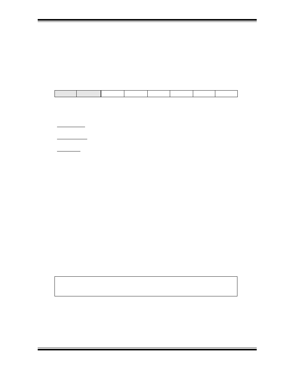
PIC18CXX2
©
7/99 Microchip Technology Inc.
Preliminary
DS39026B-page 109
13.0
CAPTURE/COMPARE/PWM
(CCP) MODULES
Each CCP (Capture/Compare/PWM) module contains
a 16-bit register which can operate as a 16-bit capture
register, as a 16-bit compare register or as a PWM
master/slave Duty Cycle register. Table 13-1 shows the
timer resources of the CCP module modes.
The operation of CCP1 is identical to that of CCP2, with
the exception of the special event trigger. Therefore,
operation of a CCP module in the following sections is
described with respect to CCP1.
Table 13-2 shows the interaction of the CCP modules.
Register 13-1: CCP1CON Register/CCP2CON Register
U-0
U-0
R/W-0
R/W-0
R/W-0
R/W-0
R/W-0
R/W-0
--
--
DCxB1
DCxB0
CCPxM3
CCPxM2
CCPxM1
CCPxM0
bit 7
bit 0
bit 7:6
Unimplemented: Read as '0'
bit 5:4
DCxB1:DCxB0: PWM Duty Cycle bit1 and bit0
Capture Mode:
Unused
Compare Mode:
Unused
PWM Mode:
These bits are the two LSbs (bit1 and bit0) of the 10-bit PWM duty cycle. The upper eight bits
(DCx9:DCx2) of the duty cycle are found in CCPRxL.
bit 3:0
CCPxM3:CCPxM0: CCPx Mode Select bits
0000
= Capture/Compare/PWM off (resets CCPx module)
0001
= Reserved
0010
= Compare mode, toggle output on match (CCPxIF bit is set)
0011
= Reserved
0100
= Capture mode, every falling edge
0101
= Capture mode, every rising edge
0110
= Capture mode, every 4th rising edge
0111
= Capture mode, every 16th rising edge
1000
= Compare mode,
Initialize CCP pin Low, on compare match force CCP pin High (CCPIF bit is set)
1001
= Compare mode,
Initialize CCP pin High, on compare match force CCP pin Low (CCPIF bit is set)
1010
= Compare mode,
Generate software interrupt on compare match
(CCPIF bit is set, CCP pin is unaffected)
1011
= Compare mode,
Trigger special event (CCPIF bit is set)
11xx
= PWM mode
Legend:
R = Readable bit
W = Writable bit
U = Unimplemented bit, read as `0'
- n = Value at POR reset
'1' = Bit is set
'0' = Bit is cleared
x = Bit is unknown
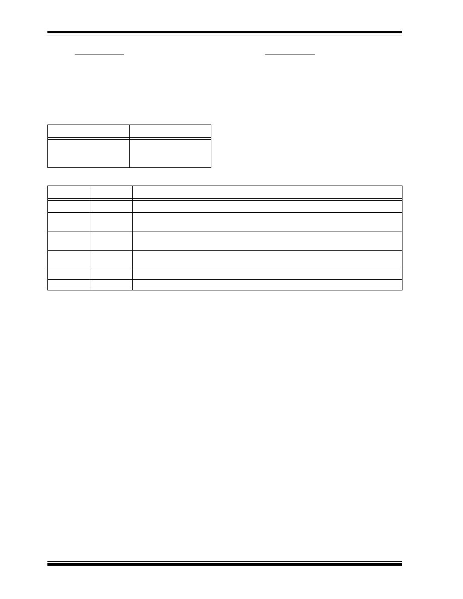
PIC18CXX2
DS39026B-page 110
Preliminary
©
7/99 Microchip Technology Inc.
13.1
CCP1 Module
Capture/Compare/PWM Register1 (CCPR1) is com-
prised of two 8-bit registers: CCPR1L (low byte) and
CCPR1H (high byte). The CCP1CON register controls
the operation of CCP1. All are readable and writable.
13.2
CCP2 Module
Capture/Compare/PWM Register2 (CCPR2) is com-
prised of two 8-bit registers: CCPR2L (low byte) and
CCPR2H (high byte). The CCP2CON register controls
the operation of CCP2. All are readable and writable.
TABLE 13-1:
CCP MODE - TIMER RESOURCE
TABLE 13-2:
INTERACTION OF TWO CCP MODULES
CCP Mode
Timer Resource
Capture
Compare
PWM
Timer1 or Timer3
Timer1 or Timer3
Timer2
CCPx Mode CCPy Mode
Interaction
Capture
Capture
TMR1 or TMR3 time-base. Time base can be different for each CCP.
Capture
Compare
The compare could be configured for the special event trigger, which clears either TMR1
or TMR3 depending upon which time base is used.
Compare
Compare
The compare(s) could be configured for the special event trigger, which clears TMR1 or
TMR3 depending upon which time base is used.
PWM
PWM
The PWMs will have the same frequency and update rate
(TMR2 interrupt).
PWM
Capture
None
PWM
Compare
None
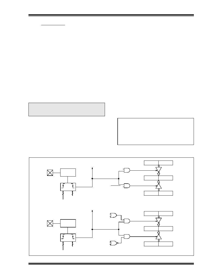
PIC18CXX2
©
7/99 Microchip Technology Inc.
Preliminary
DS39026B-page 111
13.3
Capture Mode
In Capture mode, CCPR1H:CCPR1L captures the 16-
bit value of the TMR1 or TMR3 registers when an event
occurs on pin RC2/CCP1. An event is defined as:
∑ every falling edge
∑ every rising edge
∑ every 4th rising edge
∑ every 16th rising edge
An event is selected by control bits CCP1M3:CCP1M0
(CCP1CON<3:0>). When a capture is made, the inter-
rupt request flag bit CCP1IF (PIR1<2>) is set. It must
be cleared in software. If another capture occurs before
the value in register CCPR1 is read, the old captured
value will be lost.
13.3.1
CCP PIN CONFIGURATION
In Capture mode, the RC2/CCP1 pin should be config-
ured as an input by setting the TRISC<2> bit.
13.3.2
TIMER1/TIMER3 MODE SELECTION
The timers that are to be used with the capture feature
(either Timer1 and/or Timer3) must be running in timer
mode or synchronized counter mode. In asynchronous
counter mode, the capture operation may not work.
The timer to be used with each CCP module is selected
in the T3CON register.
13.3.3
SOFTWARE INTERRUPT
When the Capture mode is changed, a false capture
interrupt may be generated. The user should keep bit
CCP1IE (PIE1<2>) clear to avoid false interrupts and
should clear the flag bit CCP1IF following any such
change in operating mode.
13.3.4
CCP PRESCALER
There are four prescaler settings, specified by bits
CCP1M3:CCP1M0. Whenever the CCP module is
turned off or the CCP module is not in capture mode,
the prescaler counter is cleared. This means that any
reset will clear the prescaler counter.
Switching from one capture prescaler to another may
generate an interrupt. Also, the prescaler counter will
not be cleared, therefore the first capture may be from
a non-zero prescaler. Example 13-1 shows the recom-
mended method for switching between capture pres-
calers. This example also clears the prescaler counter
and will not generate the "false" interrupt.
EXAMPLE 13-1: CHANGING BETWEEN
CAPTURE PRESCALERS
FIGURE 13-1: CAPTURE MODE OPERATION BLOCK DIAGRAM
Note:
If the RC2/CCP1 is configured as an out-
put, a write to the port can cause a capture
condition.
CLRF
CCP1CON, F
; Turn CCP module off
MOVLW NEW_CAPT_PS
; Load WREG with the
; new prescaler mode
; value and CCP ON
MOVWF CCP1CON
; Load CCP1CON with
; this value
CCPR1H
CCPR1L
TMR1H
TMR1L
Set flag bit CCP1IF
TMR3
Enable
Q's
CCP1CON<3:0>
CCP1 Pin
Prescaler
˜
1, 4, 16
and
edge detect
TMR3H
TMR3L
TMR1
Enable
T3CCP2
T3CCP2
CCPR2H
CCPR2L
TMR1H
TMR1L
Set flag bit CCP2IF
TMR3
Enable
Q's
CCP2CON<3:0>
CCP2 Pin
Prescaler
˜
1, 4, 16
and
edge detect
TMR3H
TMR3L
TMR1
Enable
T3CCP2
T3CCP1
T3CCP2
T3CCP1
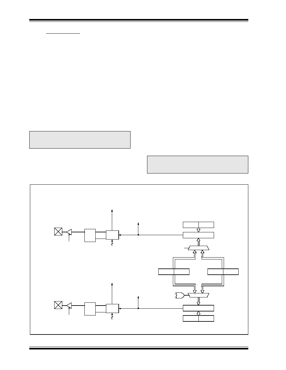
PIC18CXX2
DS39026B-page 112
Preliminary
©
7/99 Microchip Technology Inc.
13.4
Compare Mode
In Compare mode, the 16-bit CCPR1 (CCPR2) register
value is constantly compared against either the TMR1
register pair value or the TMR3 register pair value.
When a match occurs, the RC2/CCP1 (RC1/CCP2) pin
is:
∑ driven High
∑ driven Low
∑ toggle output (High to Low or Low to High)
∑ remains Unchanged
The action on the pin is based on the value of control
bits CCP1M3:CCP1M0 (CCP2M3:CCP2M0). At the
same time, interrupt flag bit CCP1IF (CCP2IF) is set.
13.4.1
CCP PIN CONFIGURATION
The user must configure the CCPx pin as an output by
clearing the appropriate TRISC bit.
13.4.2
TIMER1/TIMER3 MODE SELECTION
Timer1 and/or Timer3 must be running in Timer mode
or Synchronized Counter mode if the CCP module is
using the compare feature. In Asynchronous Counter
mode, the compare operation may not work.
13.4.3
SOFTWARE INTERRUPT MODE
When generate software interrupt is chosen, the CCP1
pin is not affected. Only a CCP interrupt is generated (if
enabled).
13.4.4
SPECIAL EVENT TRIGGER
In this mode, an internal hardware trigger is generated,
which may be used to initiate an action.
The special event trigger output of CCP1 resets the
TMR1 register pair. This allows the CCPR1 register to
effectively be a 16-bit programmable period register for
Timer1.
The special trigger output of CCPx resets either the
TMR1 or TMR3 register pair. Additionally, the CCP2
Special Event Trigger will start an A/D conversion if the
A/D module is enabled.
FIGURE 13-2: COMPARE MODE OPERATION BLOCK DIAGRAM
Note:
Clearing the CCP1CON register will force
the RC2/CCP1 compare output latch to the
default low level. This is not the data latch.
Note:
The special event trigger from the CCP2
module will not set the Timer1 or Timer3
interrupt flag bits.
CCPR1H CCPR1L
TMR1H
TMR1L
Comparator
Q
S
R
Output
Logic
Special Event Trigger
Set flag bit CCP1IF
match
RC2/CCP1
TRISC<2>
CCP1CON<3:0>
Mode Select
Output Enable
Pin
Special Event Trigger will:
Reset Timer1or Timer3, but not set Timer1 or Timer3 interrupt flag bit,
and set bit GO/DONE (ADCON0<2>)
which starts an A/D conversion (CCP2 only)
TMR3H
TMR3L
T3CCP2
CCPR2H CCPR2L
Comparator
1
0
T3CCP2
T3CCP1
Q
S
R
Output
Logic
Special Event Trigger
Set flag bit CCP2IF
match
RC1/CCP2
TRISC<1>
CCP2CON<3:0>
Mode Select
Output Enable
Pin
0
1
PIC18CXX2
©
7/99 Microchip Technology Inc.
Preliminary
DS39026B-page 113
TABLE 13-3:
REGISTERS ASSOCIATED WITH CAPTURE, COMPARE, TIMER1 AND TIMER3
Name
Bit 7
Bit 6
Bit 5
Bit 4
Bit 3
Bit 2
Bit 1
Bit 0
Value on
POR,
BOR
Value on
all other
resets
INTCON
GIE/
GIEH
PEIE/
GIEL
TMR0IE
INT0IE
RBIE
TMR0IF
INT0IF
RBIF
0000 000x
0000 000u
PIR1
PSPIF
(1)
ADIF
RCIF
TXIF
SSPIF
CCP1IF
TMR2IF
TMR1IF
0000 0000
0000 0000
PIE1
PSPIE
(1)
ADIE
RCIE
TXIE
SSPIE
CCP1IE
TMR2IE
TMR1IE
0000 0000
0000 0000
IPR1
PSPIP
(1)
ADIP
RCIP
TXIP
SSPIP
CCP1IP
TMR2IP
TMR1IP
0000 0000
0000 0000
TRISC
PORTC Data Direction Register
1111 1111
1111 1111
TMR1L
Holding register for the Least Significant Byte of the 16-bit TMR1 register
xxxx xxxx
uuuu uuuu
TMR1H
Holding register for the Most Significant Byte of the 16-bit TMR1register
xxxx xxxx
uuuu uuuu
T1CON
--
--
T1CKPS1
T1CKPS0
T1OSCEN
T1SYNC
TMR1CS
TMR1ON
--00 0000
--uu uuuu
CCPR1L
Capture/Compare/PWM register1 (LSB)
xxxx xxxx
uuuu uuuu
CCPR1H
Capture/Compare/PWM register1 (MSB)
xxxx xxxx
uuuu uuuu
CCP1CON
--
--
DC1B1
DC1B0
CCP1M3
CCP1M2
CCP1M1
CCP1M0
--00 0000
--00 0000
CCPR2L
Capture/Compare/PWM register2 (LSB)
xxxx xxxx
uuuu uuuu
CCPR2H
Capture/Compare/PWM register2 (MSB)
xxxx xxxx
uuuu uuuu
CCP2CON
--
--
DC2B1
DC2B0
CCP2M3
CCP2M2
CCP2M1
CCP2M0
--00 0000
--00 0000
PIR2
--
--
--
--
BCLIF
LVDIF
TMR3IF
CCP2IF
0000 0000
0000 0000
PIE2
--
--
--
--
BCLIE
LVDIE
TMR3IE
CCP2IE
0000 0000
0000 0000
IPR2
--
--
--
--
BCLIP
LVDIP
TMR3IP
CCP2IP
0000 0000
0000 0000
TMR3L
Holding register for the Least Significant Byte of the 16-bit TMR3 register
xxxx xxxx
uuuu uuuu
TMR3H
Holding register for the Most Significant Byte of the 16-bit TMR3 register
xxxx xxxx
uuuu uuuu
T3CON
--
T3CKPS2
T3CKPS1
T3CKPS0
T3CCP1
T3SYNC
TMR3CS
TMR3ON
-000 0000
-uuu uuuu
Legend:
x = unknown, u = unchanged,
-
= unimplemented read as '0'.
Shaded cells are not used by Capture and Timer1.
Note 1: The PSPIF, PSPIE and PSPIP bits are reserved on the PIC18C2x2 devices. Always maintain these bits clear.
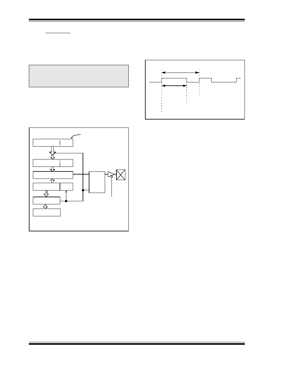
PIC18CXX2
DS39026B-page 114
Preliminary
©
7/99 Microchip Technology Inc.
13.5
PWM Mode
In Pulse Width Modulation (PWM) mode, the CCP1 pin
produces up to a 10-bit resolution PWM output. Since
the CCP1 pin is multiplexed with the PORTC data latch,
the TRISC<2> bit must be cleared to make the CCP1
pin an output.
Figure 13-3 shows a simplified block diagram of the
CCP module in PWM mode.
For a step by step procedure on how to set up the CCP
module for PWM operation, see Section 13.5.3.
FIGURE 13-3: SIMPLIFIED PWM BLOCK
DIAGRAM
A PWM output (Figure 13-4) has a time base (period)
and a time that the output stays high (duty cycle).
The frequency of the PWM is the inverse of the
period (1/period).
FIGURE 13-4: PWM OUTPUT
Note:
Clearing the CCP1CON register will force
the CCP1 PWM output latch to the default
low level. This is not the PORTC I/O data
latch.
CCPR1L
CCPR1H (Slave)
Comparator
TMR2
Comparator
PR2
(Note 1)
R
Q
S
Duty cycle registers
CCP1CON<5:4>
Clear Timer,
CCP1 pin and
latch D.C.
TRISC<2>
RC2/CCP1
Note: 8-bit timer is concatenated with 2-bit internal Q clock
or 2 bits of the prescaler to create 10-bit time-base.
Period
Duty Cycle
TMR2 = PR2
TMR2 = Duty Cycle
TMR2 = PR2

PIC18CXX2
©
7/99 Microchip Technology Inc.
Preliminary
DS39026B-page 115
13.5.1
PWM PERIOD
The PWM period is specified by writing to the PR2 reg-
ister. The PWM period can be calculated using the fol-
lowing formula:
PWM period = (PR2) + 1] ∑ 4 ∑ T
OSC
∑
(TMR2 prescale value)
PWM frequency is defined as 1 / [PWM period].
When TMR2 is equal to PR2, the following three events
occur on the next increment cycle:
∑ TMR2 is cleared
∑ The CCP1 pin is set (exception: if PWM duty
cycle = 0%, the CCP1 pin will not be set)
∑ The PWM duty cycle is latched from CCPR1L into
CCPR1H
13.5.2
PWM DUTY CYCLE
The PWM duty cycle is specified by writing to the
CCPR1L register and to the CCP1CON<5:4> bits. Up
to 10-bit resolution is available. The CCPR1L contains
the eight MSbs and the CCP1CON<5:4> contains the
two LSbs. This 10-bit value is represented by
CCPR1L:CCP1CON<5:4>. The following equation is
used to calculate the PWM duty cycle in time:
PWM duty cycle = (CCPR1L:CCP1CON<5:4>) ∑
T
OSC
∑ (TMR2 prescale value)
CCPR1L and CCP1CON<5:4> can be written to at any
time, but the duty cycle value is not latched into
CCPR1H until after a match between PR2 and TMR2
occurs (i.e., the period is complete). In PWM mode,
CCPR1H is a read-only register.
The CCPR1H register and a 2-bit internal latch are
used to double buffer the PWM duty cycle. This double
buffering is essential for glitchless PWM operation.
When the CCPR1H and 2-bit latch match TMR2 con-
catenated with an internal 2-bit Q clock or 2 bits of the
TMR2 prescaler, the CCP1 pin is cleared.
Maximum PWM resolution (bits) for a given PWM fre-
quency:
Note:
The Timer2 postscaler (see Section 10.0)
is not used in the determination of the
PWM frequency. The postscaler could be
used to have a servo update rate at a dif-
ferent frequency than the PWM output.
Note:
If the PWM duty cycle value is longer than
the PWM period, the CCP1 pin will not be
cleared.
F
OSC
F
PWM
---------------
log
2
( )
log
----------------------------- bits
=
PIC18CXX2
DS39026B-page 116
Preliminary
©
7/99 Microchip Technology Inc.
13.5.3
SET-UP FOR PWM OPERATION
The following steps should be taken when configuring
the CCP module for PWM operation:
1.
Set the PWM period by writing to the PR2 regis-
ter.
2.
Set the PWM duty cycle by writing to the
CCPR1L register and CCP1CON<5:4> bits.
3.
Make the CCP1 pin an output by clearing the
TRISC<2> bit.
4.
Set the TMR2 prescale value and enable Timer2
by writing to T2CON.
5.
Configure the CCP1 module for PWM operation.
TABLE 13-4:
EXAMPLE PWM FREQUENCIES AND RESOLUTIONS AT 40 MHz
TABLE 13-5:
REGISTERS ASSOCIATED WITH PWM AND TIMER2
PWM Frequency
2.44 kHz
9.76 kHz
19.53 kHz
39.06 kHz
78.12 kHz
208.3 kHz
Timer Prescaler (1, 4, 16)
16
4
1
1
1
1
PR2 Value
0xFF
0xFF
0xFF
0x3F
0x1F
0x17
Maximum Resolution (bits)
10
10
10
8
7
5.5
Name
Bit 7
Bit 6
Bit 5
Bit 4
Bit 3
Bit 2
Bit 1
Bit 0
Value on
POR,
BOR
Value on
all other
resets
INTCON
GIE/
GIEH
PEIE/
GIEL
TMR0IE
INT0IE
RBIE
TMR0IF
INT0IF
RBIF
0000 000x
0000 000u
PIR1
PSPIF
(1)
ADIF
RCIF
TXIF
SSPIF
CCP1IF
TMR2IF
TMR1IF
0000 0000
0000 0000
PIE1
PSPIE
(1)
ADIE
RCIE
TXIE
SSPIE
CCP1IE
TMR2IE
TMR1IE
0000 0000
0000 0000
IPR1
PSPIP
(1)
ADIP
RCIP
TXIP
SSPIP
CCP1IP
TMR2IP
TMR1IP
0000 0000
0000 0000
TRISC
PORTC Data Direction Register
1111 1111
1111 1111
TMR2
Timer2 module's register
0000 0000
0000 0000
PR2
Timer2 module's period register
1111 1111
1111 1111
T2CON
--
TOUTPS3
TOUTPS2
TOUTPS1
TOUTPS0
TMR2ON
T2CKPS1
T2CKPS0
-000 0000
-000 0000
CCPR1L
Capture/Compare/PWM register1 (LSB)
xxxx xxxx
uuuu uuuu
CCPR1H
Capture/Compare/PWM register1 (MSB)
xxxx xxxx
uuuu uuuu
CCP1CON
--
--
DC1B1
DC1B0
CCP1M3
CCP1M2
CCP1M1
CCP1M0
--00 0000
--00 0000
CCPR2L
Capture/Compare/PWM register2 (LSB)
xxxx xxxx
uuuu uuuu
CCPR2H
Capture/Compare/PWM register2 (MSB)
xxxx xxxx
uuuu uuuu
CCP2CON
--
--
DC2B1
DC2B0
CCP2M3
CCP2M2
CCP2M1
CCP2M0
--00 0000
--00 0000
Legend:
x
= unknown,
u
= unchanged,
--
= unimplemented read as '0'.
Shaded cells are not used by PWM and Timer2.
Note 1: The PSPIF, PSPIE and PSPIP bits are reserved on the PIC18C2X2 devices. Always maintain these bits clear.

PIC18CXX2
©
7/99 Microchip Technology Inc.
Preliminary
DS39026B-page 117
14.0
MASTER SYNCHRONOUS
SERIAL PORT (MSSP)
MODULE
14.1
Master SSP (MSSP) Module Overview
The Master Synchronous Serial Port (MSSP) module is
a serial interface useful for communicating with other
peripheral or microcontroller devices. These peripheral
devices may be Serial EEPROMs, shift registers, dis-
play drivers, A/D converters, etc. The MSSP module
can operate in one of two modes:
∑ Serial Peripheral Interface (SPI)
∑ Inter-Integrated Circuit (I
2
C)
- Full Master Mode
- Slave mode (with general address call)
The I
2
C interface supports the following modes in hard-
ware:
∑ Master mode
∑ Multi-master mode
∑ Slave mode

PIC18CXX2
DS39026B-page 118
Preliminary
©
7/99 Microchip Technology Inc.
14.2
Control Registers
The MSSP module has three associated registers.
These include a status register and two control regis-
ters.
Register 14-1: SSPSTAT: MSSP Status Register
R/W-0
R/W-0
R-0
R-0
R-0
R-0
R-0
R-0
SMP
CKE
D/A
P
S
R/W
UA
BF
bit 7
bit 0
bit 7
SMP: Sample bit
SPI Master Mode
1
= Input data sampled at end of data output time
0
= Input data sampled at middle of data output time
SPI Slave Mode
SMP must be cleared when SPI is used in slave mode
In I
2
C master or slave mode:
1
= Slew rate control disabled for standard speed mode (100 kHz and 1 MHz)
0
= Slew rate control enabled for high speed mode (400 kHz)
bit 6
CKE: SPI Clock Edge Select
CKP = 0
1
= Data transmitted on rising edge of SCK
0
= Data transmitted on falling edge of SCK
CKP = 1
1
= Data transmitted on falling edge of SCK
0
= Data transmitted on rising edge of SCK
bit 5
D/A: Data/Address bit (I
2
C mode only)
1
= Indicates that the last byte received or transmitted was data
0
= Indicates that the last byte received or transmitted was address
bit 4
P: Stop bit
(I
2
C mode only. This bit is cleared when the MSSP module is disabled, SSPEN is cleared)
1
= Indicates that a stop bit has been detected last (this bit is '0' on RESET)
0
= Stop bit was not detected last
bit 3
S: Start bit
(I
2
C mode only. This bit is cleared when the MSSP module is disabled, SSPEN is cleared)
1
= Indicates that a start bit has been detected last (this bit is '0' on RESET)
0
= Start bit was not detected last
bit 2
R/W: Read/Write bit information (I
2
C mode only)
This bit holds the R/W bit information following the last address match. This bit is only valid from the address
match to the next start bit, stop bit, or not ACK bit.
In I
2
C slave mode:
1
= Read
0
= Write
In I
2
C master mode:
1
= Transmit is in progress
0
= Transmit is not in progress.
OR-ing this bit with SEN, RSEN, PEN, RCEN, or ACKEN will indicate if the MSSP is in IDLE mode.
bit 1
UA: Update Address (10-bit I
2
C mode only)
1
= Indicates that the user needs to update the address in the SSPADD register
0
= Address does not need to be updated
bit 0
BF: Buffer Full Status bit
Receive (SPI and I
2
C modes)
1
= Receive complete, SSPBUF is full
0
= Receive not complete, SSPBUF is empty
Transmit (I
2
C mode only)
1
= Data Transmit in progress (does not include the ACK and stop bits), SSPBUF is full
0
= Data Transmit complete (does not include the ACK and stop bits), SSPBUF is empty
Legend:
R = Readable bit
W = Writable bit
U = Unimplemented bit, read as `0'
- n = Value at POR reset
'1' = Bit is set
'0' = Bit is cleared
x = Bit is unknown

PIC18CXX2
©
7/99 Microchip Technology Inc.
Preliminary
DS39026B-page 119
Register 14-2: SSPCON1: MSSP Control Register1
R/W-0
R/W-0
R/W-0
R/W-0
R/W-0
R/W-0
R/W-0
R/W-0
WCOL
SSPOV
SSPEN
CKP
SSPM3
SSPM2
SSPM1
SSPM0
bit 7
bit 0
bit 7
WCOL: Write Collision Detect bit
Master Mode:
1
= A write to the SSPBUF register was attempted while the I
2
C conditions were not valid for a transmission
to be started
0
= No collision
Slave Mode:
1
= The SSPBUF register is written while it is still transmitting the previous word must be cleared in software)
0
= No collision
bit 6
SSPOV: Receive Overflow Indicator bit
In SPI mode:
1
= A new byte is received while the SSPBUF register is still holding the previous data. In case of overflow,
the data in SSPSR is lost. Overflow can only occur in slave mode. In slave mode the user must read the
SSPBUF, even if only transmitting data, to avoid setting overflow. In master mode the overflow bit is not
set since each new reception (and transmission) is initiated by writing to the SSPBUF register. (Must be
cleared in software)
0
= No overflow
In I
2
C mode:
1
= A byte is received while the SSPBUF register is still holding the previous byte. SSPOV is a "don't care"
in transmit mode. (Must be cleared in software)
0
= No overflow
bit 5
SSPEN: Synchronous Serial Port Enable bit
In both modes, when enabled, these pins must be properly configured as input or output.
In SPI mode:
1
= Enables serial port and configures SCK, SDO, SDI, and SS as the source of the serial port pins
0
= Disables serial port and configures these pins as I/O port pins
In I
2
C mode:
1
= Enables the serial port and configures the SDA and SCL pins as the source of the serial port pins
0
= Disables serial port and configures these pins as I/O port pins
bit 4
CKP: Clock Polarity Select bit
In SPI mode:
1
= Idle state for clock is a high level
0
= Idle state for clock is a low level
In I
2
C slave mode:
SCK release control
1
= Enable clock
0
= Holds clock low (clock stretch) (Used to ensure data setup time)
In I
2
C master mode
Unused in this mode
bit 3 - 0
SSPM3:SSPM0: Synchronous Serial Port Mode Select bits
0000
= SPI master mode, clock = F
OSC
/4
0001
= SPI master mode, clock = F
OSC
/16
0010
= SPI master mode, clock = F
OSC
/64
0011
= SPI master mode, clock = TMR2 output/2
0100
= SPI slave mode, clock = SCK pin. SS pin control enabled.
0101
= SPI slave mode, clock = SCK pin. SS pin control disabled. SS can be used as I/O pin
0110
= I
2
C slave mode, 7-bit address
0111
= I
2
C slave mode, 10-bit address
1000
= I
2
C master mode, clock = F
OSC
/ (4 * (SSPADD+1) )
1001
= Reserved
1010
= Reserved
1011
= I
2
C firmware controlled Master mode (Slave idle)
1100
= Reserved
1101
= Reserved
1110
= I
2
C slave mode, 7-bit address with start and stop bit interrupts enabled
1111
= I
2
C slave mode, 10-bit address with start and stop bit interrupts enabled
Legend:
R = Readable bit
W = Writable bit
U = Unimplemented bit, read as `0'
- n = Value at POR reset
'1' = Bit is set
'0' = Bit is cleared
x = Bit is unknown

PIC18CXX2
DS39026B-page 120
Preliminary
©
7/99 Microchip Technology Inc.
Register 14-3: SSPCON2: MSSP Control Register2
R/W-0
R/W-0
R/W-0
R/W-0
R/W-0
R/W-0
R/W-0
R/W-0
GCEN
ACKSTAT
ACKDT
ACKEN
RCEN
PEN
RSEN
SEN
bit 7
bit 0
bit 7
GCEN: General Call Enable bit (In I
2
C slave mode only)
1
= Enable interrupt when a general call address (0000h) is received in the SSPSR
0
= General call address disabled
bit 6
ACKSTAT: Acknowledge Status bit (In I
2
C master mode only)
In master transmit mode:
1
= Acknowledge was not received from slave
0
= Acknowledge was received from slave
bit 5
ACKDT: Acknowledge Data bit (In I
2
C master mode only)
In master receive mode:
Value that will be transmitted when the user initiates an Acknowledge sequence at the end of
a receive.
1
= Not Acknowledge
0
= Acknowledge
bit 4
ACKEN: Acknowledge Sequence Enable bit (In I
2
C master mode only)
In master receive mode:
1
= Initiate Acknowledge sequence on SDA and SCL pins, and transmit ACKDT data bit.
Automatically cleared by hardware.
0
= Acknowledge sequence idle
bit 3
RCEN: Receive Enable bit (In I
2
C master mode only)
1
= Enables Receive mode for I
2
C
0
= Receive idle
bit 2
PEN: Stop Condition Enable bit (In I
2
C master mode only)
SCK release control
1
= Initiate Stop condition on SDA and SCL pins. Automatically cleared by hardware.
0
= Stop condition idle
bit 1
RSEN: Repeated Start Condition Enabled bit (In I
2
C master mode only)
1
= Initiate Repeated Start condition on SDA and SCL pins. Automatically cleared by hardware.
0
= Repeated Start condition idle.
bit 0
SEN: Start Condition Enabled bit (In I
2
C master mode only)
1
= Initiate Start condition on SDA and SCL pins. Automatically cleared by hardware.
0
= Start condition idle
Note:
For bits ACKEN, RCEN, PEN, RSEN, SEN: If the I
2
C module is not in the idle mode,
this bit may not be set (no spooling) and the SSPBUF may not be written (or writes
to the SSPBUF are disabled).
Legend:
R = Readable bit
W = Writable bit
U = Unimplemented bit, read as `0'
- n = Value at POR reset
'1' = Bit is set
'0' = Bit is cleared
x = Bit is unknown
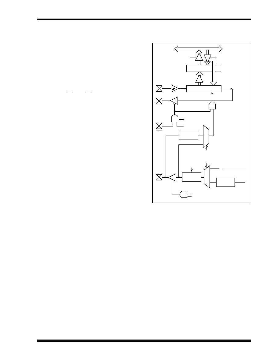
PIC18CXX2
©
7/99 Microchip Technology Inc.
Preliminary
DS39026B-page 121
14.2.1
SPI Mode
The SPI mode allows 8-bits of data to be synchro-
nously transmitted and received simultaneously. All
four modes of SPI are supported. To accomplish com-
munication, typically three pins are used:
∑ Serial Data Out (SDO) - RC5/SDO
∑ Serial Data In (SDI) - RC4/SDI/SDA
∑ Serial Clock (SCK) - RC3/SCK/SCL/LVOIN
Additionally a fourth pin may be used when in a slave
mode of operation:
∑ Slave Select (SS) - RA5/SS/AN4
14.2.1.1
OPERATION
When initializing the SPI, several options need to be
specified. This is done by programming the appropriate
control bits (SSPCON1<5:0>) and SSPSTAT<7:6>.
These control bits allow the following to be specified:
∑ Master Mode (SCK is the clock output)
∑ Slave Mode (SCK is the clock input)
∑ Clock Polarity (Idle state of SCK)
∑ Data input sample phase (middle or end of data
output time)
∑ Clock edge (output data on rising/falling edge of
SCK)
∑ Clock Rate (Master mode only)
∑ Slave Select Mode (Slave mode only)
Figure 14-1 shows the block diagram of the MSSP
module, when in SPI mode.
FIGURE 14-1: MSSP BLOCK DIAGRAM
(SPI MODE)
The MSSP consists of a transmit/receive Shift Register
(SSPSR) and a buffer register (SSPBUF). The SSPSR
shifts the data in and out of the device, MSb first. The
SSPBUF holds the data that was written to the SSPSR,
until the received data is ready. Once the 8 bits of data
have been received, that byte is moved to the SSPBUF
register. Then the buffer full detect bit, BF
(SSPSTAT<0>), and the interrupt flag bit, SSPIF, are
set. This double buffering of the received data (SSP-
BUF) allows the next byte to start reception before
reading the data that was just received. Any write to the
SSPBUF register during transmission/reception of data
will be ignored, and the write collision detect bit, WCOL
(SSPCON1<7>), will be set. User software must clear
the WCOL bit so that it can be determined if the follow-
ing write(s) to the SSPBUF register completed suc-
cessfully.
Read
Write
Internal
data bus
SSPSR reg
SSPBUF reg
SSPM3:SSPM0
bit0
shift
clock
SS Control
Enable
Edge
Select
Clock Select
TMR2 output
T
OSC
Prescaler
4, 16, 64
2
Edge
Select
2
4
Data to TX/RX in SSPSR
TRIS bit
2
SMP:CKE
SDI
SDO
SS
SCK
( )

PIC18CXX2
DS39026B-page 122
Preliminary
©
7/99 Microchip Technology Inc.
When the application software is expecting to receive
valid data, the SSPBUF should be read before the next
byte of data to transfer is written to the SSPBUF. Buffer
full bit, BF (SSPSTAT<0>), indicates when SSPBUF
has been loaded with the received data (transmission
is complete). When the SSPBUF is read, the BF bit is
cleared. This data may be irrelevant if the SPI is only a
transmitter. Generally the MSSP Interrupt is used to
determine when the transmission/reception has
completed. The SSPBUF must be read and/or written.
If the interrupt method is not going to be used, then
software polling can be done to ensure that a write
collision does not occur. Example 14-1 shows the
loading of the SSPBUF (SSPSR) for data transmission.
EXAMPLE 14-1: LOADING THE SSPBUF (SSPSR) REGISTER
The SSPSR is not directly readable or writable, and can
only be accessed by addressing the SSPBUF register.
Additionally, the MSSP status register (SSPSTAT) indi-
cates the various status conditions.
14.2.1.2
ENABLING SPI I/O
To enable the serial port, SSP Enable bit, SSPEN
(SSPCON1<5>), must be set. To reset or reconfigure
SPI mode, clear the SSPEN bit, re-initialize the SSP-
CON registers, and then set the SSPEN bit. This con-
figures the SDI, SDO, SCK, and SS pins as serial port
pins. For the pins to behave as the serial port function,
some must have their data direction bits (in the TRIS
register) appropriately programmed. That is:
∑ SDI is automatically controlled by the SPI module
∑ SDO must have TRISC<5> bit cleared
∑ SCK (Master mode) must have TRISC<3> bit
cleared
∑ SCK (Slave mode) must have TRISC<3> bit set
∑ SS must have TRISC<4> bit set
Any serial port function that is not desired may be over-
ridden by programming the corresponding data direc-
tion (TRIS) register to the opposite value.
14.2.1.3
TYPICAL CONNECTION
Figure 14-2 shows a typical connection between two
microcontrollers. The master controller (Processor 1)
initiates the data transfer by sending the SCK signal.
Data is shifted out of both shift registers on their pro-
grammed clock edge, and latched on the opposite edge
of the clock. Both processors should be programmed to
same Clock Polarity (CKP), then both controllers would
send and receive data at the same time. Whether the
data is meaningful (or dummy data) depends on the
application software. This leads to three scenarios for
data transmission:
∑ Master sends data
--
Slave sends dummy data
∑ Master sends data
--
Slave sends data
∑ Master sends dummy data
--
Slave sends data
LOOP BTFSS SSPSTAT, BF ;Has data been received (transmit complete)?
GOTO LOOP ;No
MOVF SSPBUF, W ;WREG reg = contents of SSPBUF
MOVWF RXDATA ;Save in user RAM, if data is meaningful
MOVF TXDATA, W ;W reg = contents of TXDATA
MOVWF SSPBUF ;New data to xmit
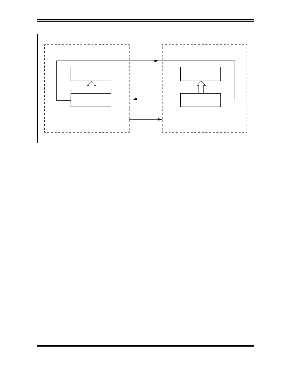
PIC18CXX2
©
7/99 Microchip Technology Inc.
Preliminary
DS39026B-page 123
FIGURE 14-2: SPI MASTER/SLAVE CONNECTION
Serial Input Buffer
(SSPBUF)
Shift Register
(SSPSR)
MSb
LSb
SDO
SDI
PROCESSOR 1
SCK
SPI Master SSPM3:SSPM0 =
00xxb
Serial Input Buffer
(SSPBUF)
Shift Register
(SSPSR)
LSb
MSb
SDI
SDO
PROCESSOR 2
SCK
SPI Slave SSPM3:SSPM0 =
010xb
Serial Clock
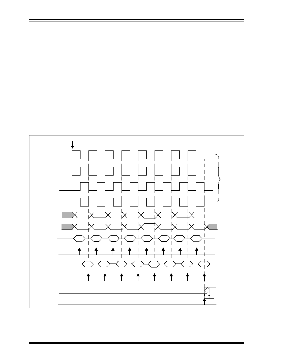
PIC18CXX2
DS39026B-page 124
Preliminary
©
7/99 Microchip Technology Inc.
14.2.1.4
MASTER MODE
The master can initiate the data transfer at any time
because it controls the SCK. The master determines
when the slave (Processor 2, Figure 14-2) is to broad-
cast data by the software protocol.
In master mode the data is transmitted/received as
soon as the SSPBUF register is written to. If the SPI is
only going to receive, the SDO output could be disabled
(programmed as an input). The SSPSR register will
continue to shift in the signal present on the SDI pin at
the programmed clock rate. As each byte is received, it
will be loaded into the SSPBUF register as if a normal
received byte (interrupts and status bits appropriately
set). This could be useful in receiver applications as a
"line activity monitor" mode.
The clock polarity is selected by appropriately program-
ming the CKP bit (SSPCON1<4>). This then would give
waveforms for SPI communication as shown in
Figure 14-3, Figure 14-5, and Figure 14-6 where the
MSB is transmitted first. In master mode, the SPI clock
rate (bit rate) is user programmable to be one of the fol-
lowing:
∑ F
OSC
/4 (or T
CY
)
∑ F
OSC
/16 (or 4 ∑ T
CY
)
∑ F
OSC
/64 (or 16 ∑ T
CY
)
∑ Timer2 output/2
This allows a maximum data rate (at 40 MHz) of 10.00
Mbps.
Figure 14-3 Shows the waveforms for master mode.
When the CKE bit is set, the SDO data is valid before
there is a clock edge on SCK. The change of the input
sample is shown based on the state of the SMP bit. The
time when the SSPBUF is loaded with the received
data is shown.
FIGURE 14-3: SPI MODE WAVEFORM (MASTER MODE)
SCK
(CKP = 0
SCK
(CKP = 1
SCK
(CKP = 0
SCK
(CKP = 1
4 clock
modes
Input
Sample
Input
Sample
SDI
bit7
bit0
SDO
bit7
bit6
bit5
bit4
bit3
bit2
bit1
bit0
bit7
bit0
SDI
SSPIF
(SMP = 1)
(SMP = 0)
(SMP = 1)
CKE = 1)
CKE = 0)
CKE = 1)
CKE = 0)
(SMP = 0)
Write to
SSPBUF
SSPSR to
SSPBUF
SDO
bit7
bit6
bit5
bit4
bit3
bit2
bit1
bit0
(CKE = 0)
(CKE = 1)
Next Q4 cycle
after Q2
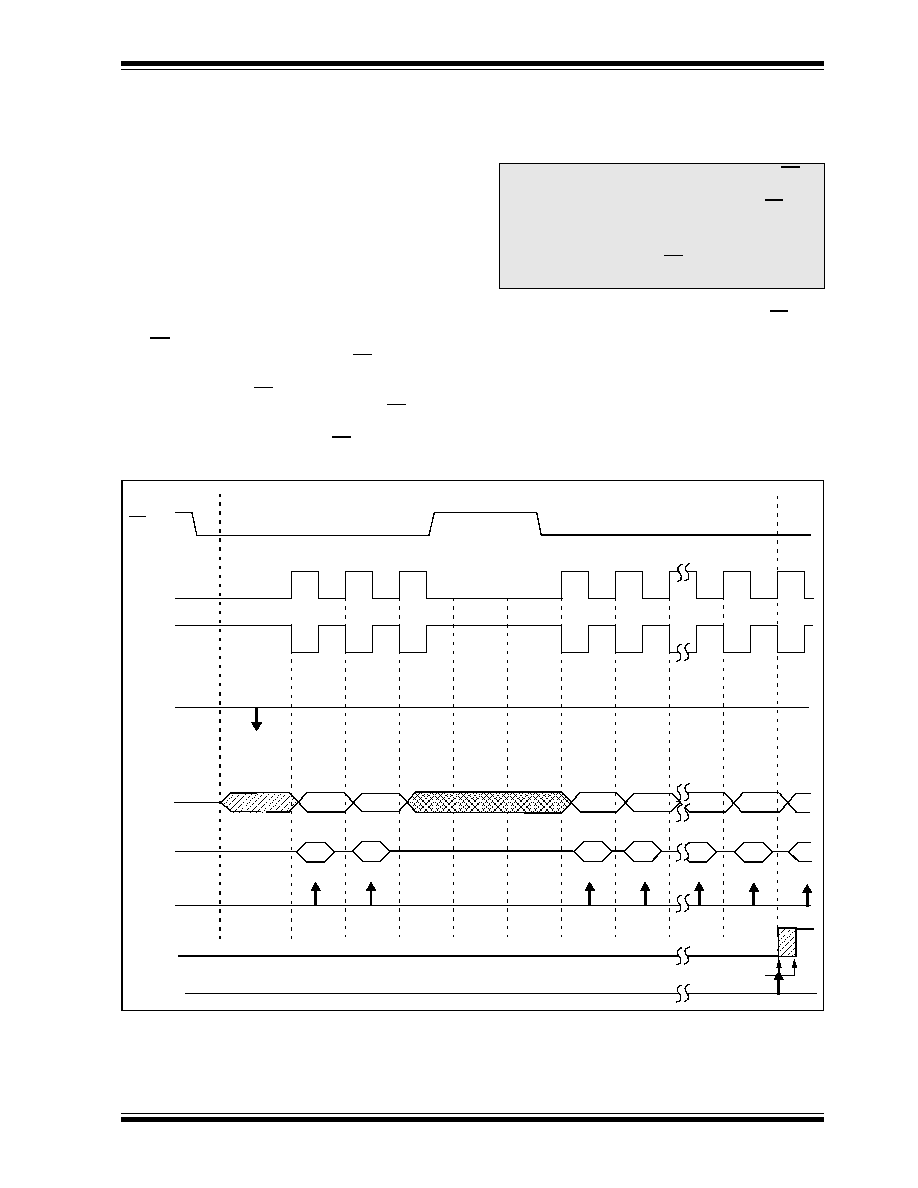
PIC18CXX2
©
7/99 Microchip Technology Inc.
Preliminary
DS39026B-page 125
14.2.1.5
SLAVE MODE
In slave mode, the data is transmitted and received as
the external clock pulses appear on SCK. When the
last bit is latched, the SSPIF interrupt flag bit is set.
While in slave mode the external clock is supplied by
the external clock source on the SCK pin. This external
clock must meet the minimum high and low times as
specified in the electrical specifications.
While in sleep mode, the slave can transmit/receive
data. When a byte is receive the device will wake-up
from sleep.
14.2.1.6
SLAVE SELECT SYNCHRONIZATION
The SS pin allows a synchronous slave mode. The
SPI must be in slave mode with SS pin control
enabled (SSPCON1<3:0> = 04h). The pin must not
be driven low for the SS pin to function as an input.
The Data Latch must be high. When the SS pin is
low, transmission and reception are enabled and
the SDO pin is driven. When the SS pin goes high,
the SDO pin is no longer driven, even if in the mid-
dle of a transmitted byte, and becomes a floating
output. External pull-up/ pull-down resistors may be
desirable, depending on the application.
When the SPI module resets, the bit counter is forced
to 0. This can be done by either by forcing the SS pin to
a high level or clearing the SSPEN bit.
To emulate two-wire communication, the SDO pin can
be connected to the SDI pin. When the SPI needs to
operate as a receiver the SDO pin can be configured as
an input. This disables transmissions from the SDO.
The SDI can always be left as an input (SDI function)
since it cannot create a bus conflict.
FIGURE 14-4: SLAVE SYNCHRONIZATION WAVEFORM
Note 1: When the SPI is in Slave Mode with SS pin
control enabled, (SSPCON<3:0> =
0100
)
the SPI module will reset if the SS pin is
set to V
DD
.
Note 2: If the SPI is used in Slave Mode with CKE
set, then the SS pin control must be
enabled.
SCK
(CKP = 1
SCK
(CKP = 0
Input
Sample
SDI
bit7
SDO
bit7
bit6
bit7
SSPIF
Interrupt
(SMP = 0)
CKE = 0)
CKE = 0)
(SMP = 0)
Write to
SSPBUF
SSPSR to
SSPBUF
SS
Flag
bit0
bit7
bit0
Next Q4 cycle
after Q2
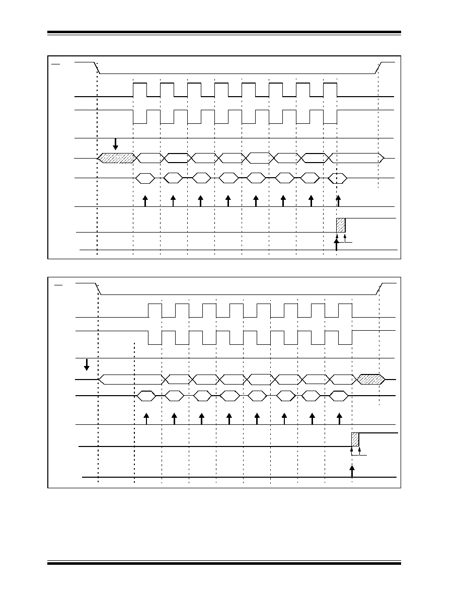
PIC18CXX2
DS39026B-page 126
Preliminary
©
7/99 Microchip Technology Inc.
FIGURE 14-5: SPI MODE WAVEFORM (SLAVE MODE WITH CKE = 0)
FIGURE 14-6: SPI MODE WAVEFORM (SLAVE MODE WITH CKE = 1)
SCK
(CKP = 1
SCK
(CKP = 0
Input
Sample
SDI
bit7
bit0
SDO
bit7
bit6
bit5
bit4
bit3
bit2
bit1
bit0
SSPIF
Interrupt
(SMP = 0)
CKE = 0)
CKE = 0)
(SMP = 0)
Write to
SSPBUF
SSPSR to
SSPBUF
SS
Flag
optional
Next Q4 cycle
after Q2
SCK
(CKP = 1
SCK
(CKP = 0
Input
Sample
SDI
bit7
bit0
SDO
bit7
bit6
bit5
bit4
bit3
bit2
bit1
bit0
SSPIF
Interrupt
(SMP = 0)
CKE = 1)
CKE = 1)
(SMP = 0)
Write to
SSPBUF
SSPSR to
SSPBUF
SS
Flag
not optional
Next Q4 cycle
after Q2
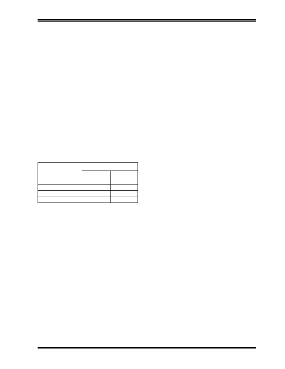
PIC18CXX2
©
7/99 Microchip Technology Inc.
Preliminary
DS39026B-page 127
14.2.1.7
SLEEP OPERATION
In master mode all module clocks are halted, and the
transmission/reception will remain in that state until the
device wakes from sleep. After the device returns to
normal mode, the module will continue to transmit/
receive data.
In slave mode, the SPI transmit/receive shift register
operates asynchronously to the device. This allows the
device to be placed in sleep mode, and data to be
shifted into the SPI transmit/receive shift register.
When all 8-bits have been received, the MSSP interrupt
flag bit will be set and if enabled will wake the device
from sleep.
14.2.1.8
EFFECTS OF A RESET
A reset disables the MSSP module and terminates the
current transfer.
14.2.1.9
BUS MODE COMPATIBILITY
Table 14-1 shows the compatibility between the stan-
dard SPI modes and the states the the CKP and CKE
control bits.
TABLE 14-1:
SPI BUS MODES
There is also a SMP bit which controls when the data is
sampled.
Standard SPI Mode
Terminology
Control Bits State
CKP
CKE
0, 0
0
1
0, 1
0
0
1, 0
1
1
1, 1
1
0
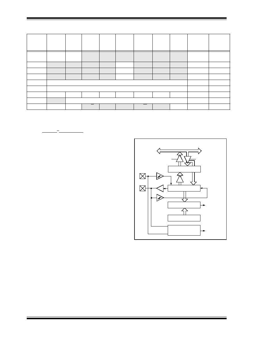
PIC18CXX2
DS39026B-page 128
Preliminary
©
7/99 Microchip Technology Inc.
TABLE 14-2:
REGISTERS ASSOCIATED WITH SPI OPERATION
14.3
MSSP I
2
C Operation
The MSSP module in I
2
C mode fully implements all
master and slave functions (including general call sup-
port) and provides interrupts on start and stop bits in
hardware to determine a free bus (multi-master func-
tion). The MSSP module implements the standard
mode specifications, as well as 7-bit and 10-bit
addressing.
Two pins are used for data transfer. These are the RC3/
SCK/SCL pin, which is the clock (SCL), and the RC4/
SDI/SDA pin, which is the data (SDA). The user must
configure these pins as inputs or outputs through the
TRISC<4:3> bits.
The MSSP module functions are enabled by setting
MSSP Enable bit SSPEN (SSPCON<5>).
FIGURE 14-7: MSSP BLOCK DIAGRAM
(I
2
C MODE)
The MSSP module has six registers for I
2
C operation.
These are the:
∑ MSSP Control Register1 (SSPCON1)
∑ MSSP Control Register2 (SSPCON2)
∑ MSSP Status Register (SSPSTAT)
∑ Serial Receive/Transmit Buffer (SSPBUF)
∑ MSSP Shift Register (SSPSR) - Not directly
accessible
∑ MSSP Address Register (SSPADD)
Name
Bit 7
Bit 6
Bit 5
Bit 4
Bit 3
Bit 2
Bit 1
Bit 0
Value on
POR,
BOR
Value on
all other
resets
INTCON
GIE/
GIEH
PEIE/
GIEL
TMR0IE
INT0IE
RBIE
TMR0IF
INT0IF
RBIF
0000 000x
0000 000u
PIR1
PSPIF
(1)
ADIF
RCIF
TXIF
SSPIF
CCP1IF
TMR2IF
TMR1IF
0000 0000
0000 0000
PIE1
PSPIE
(1)
ADIE
RCIE
TXIE
SSPIE
CCP1IE
TMR2IE TMR1IE
0000 0000
0000 0000
IPR1
PSPIP
(1)
ADIP
RCIP
TXIP
SSPIP
CCP1IP
TMR2IP TMR1IP
0000 0000
0000 0000
TRISC
PORTC Data Direction Register
1111 1111
1111 1111
SSPBUF
Synchronous Serial Port Receive Buffer/Transmit Register
xxxx xxxx
uuuu uuuu
SSPCON
WCOL
SSPOV
SSPEN
CKP
SSPM3
SSPM2
SSPM1
SSPM0
0000 0000
0000 0000
TRISA
--
PORTA Data Direction Register
--11 1111
--11 1111
SSPSTAT
SMP
CKE
D/A
P
S
R/W
UA
BF
0000 0000
0000 0000
Legend: x = unknown, u = unchanged,
-
= unimplemented read as '0'.
Shaded cells are not used by the MSSP in SPI mode.
Note 1: The PSPIF, PSPIE and PSPIP bits are reserved on the PIC18C2X2 devices. Always maintain these bits clear.
Read
Write
SSPSR reg
Match detect
SSPADD reg
Start and
Stop bit detect
SSPBUF reg
Internal
Data Bus
Addr Match
Set, Reset
S, P bits
(SSPSTAT reg)
RC3/SCK/SCL
RC4/
Shift
Clock
MSb
SDI/
LSb
SDA

PIC18CXX2
©
7/99 Microchip Technology Inc.
Preliminary
DS39026B-page 129
The SSPCON1 register allows control of the I
2
C oper-
ation. Four mode selection bits (SSPCON<3:0>) allow
one of the following I
2
C modes to be selected:
∑ I
2
C Master mode, clock = OSC/4 (SSPADD +1)
∑ I
2
C Slave mode (7-bit address)
∑ I
2
C Slave mode (10-bit address)
∑ I
2
C Slave mode (7-bit address), with start and
stop bit interrupts enabled
∑ I
2
C Slave mode (10-bit address), with start and
stop bit interrupts enabled
∑ I
2
C Firmware controlled master operation, slave
is idle
Selection of any I
2
C mode, with the SSPEN bit set,
forces the SCL and SDA pins to be open drain, pro-
vided these pins are programmed to inputs by setting
the appropriate TRISC bits.
14.3.1
SLAVE MODE
In slave mode, the SCL and SDA pins must be config-
ured as inputs (TRISC<4:3> set). The MSSP module
will override the input state with the output data when
required (slave-transmitter).
When an address is matched or the data transfer after
an address match is received, the hardware automati-
cally will generate the acknowledge (ACK) pulse and
load the SSPBUF register with the received value cur-
rently in the SSPSR register.
There are certain conditions that will cause the MSSP
module not to give this ACK pulse. These are if either
(or both):
a)
The buffer full bit BF (SSPSTAT<0>) was set
before the transfer was received.
b)
The overflow bit SSPOV (SSPCON<6>) was set
before the transfer was received.
In this case, the SSPSR register value is not loaded
into the SSPBUF, but bit SSPIF (PIR1<3>) is set. The
BF bit is cleared by reading the SSPBUF register, while
bit SSPOV is cleared through software.
The SCL clock input must have a minimum high and
low for proper operation. The high and low times of the
I
2
C specification, as well as the requirement of the
MSSP module, is shown in timing parameter #100 and
parameter #101.
14.3.1.1
ADDRESSING
Once the MSSP module has been enabled, it waits for
a START condition to occur. Following the START con-
dition, the 8-bits are shifted into the SSPSR register. All
incoming bits are sampled with the rising edge of the
clock (SCL) line. The value of register SSPSR<7:1> is
compared to the value of the SSPADD register. The
address is compared on the falling edge of the eighth
clock (SCL) pulse. If the addresses match, and the BF
and SSPOV bits are clear, the following events occur:
a)
The SSPSR register value is loaded into the
SSPBUF register.
b)
The buffer full bit BF is set.
c)
An ACK pulse is generated.
d)
MSSP interrupt flag bit SSPIF (PIR1<3>) is set
(interrupt is generated if enabled) on the falling
edge of the ninth SCL pulse.
In 10-bit address mode, two address bytes need to be
received by the slave. The five Most Significant bits
(MSbs) of the first address byte specify if this is a 10-bit
address. Bit R/W (SSPSTAT<2>) must specify a write
so the slave device will receive the second address
byte. For a 10-bit address, the first byte would equal
`1111 0 A9 A8 0', where A9 and A8 are the two MSbs
of the address. The sequence of events for 10-bit
address is as follows with steps 7- 9 for slave-transmit-
ter:
1.
Receive first (high) byte of Address (bits SSPIF,
BF and bit UA (SSPSTAT<1>) are set).
2.
Update the SSPADD register with second (low)
byte of Address (clears bit UA and releases the
SCL line).
3.
Read the SSPBUF register (clears bit BF) and
clear flag bit SSPIF.
4.
Receive second (low) byte of Address (bits
SSPIF, BF, and UA are set).
5.
Update the SSPADD register with the first (high)
byte of Address. If match releases SCL line, this
will clear bit UA.
6.
Read the SSPBUF register (clears bit BF) and
clear flag bit SSPIF.
7.
Receive repeated START condition.
8.
Receive first (high) byte of Address (bits SSPIF
and BF are set).
9.
Read the SSPBUF register (clears bit BF) and
clear flag bit SSPIF.
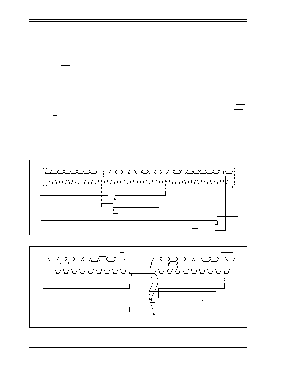
PIC18CXX2
DS39026B-page 130
Preliminary
©
7/99 Microchip Technology Inc.
14.3.1.2
RECEPTION
When the R/W bit of the address byte is clear and an
address match occurs, the R/W bit of the SSPSTAT
register is cleared. The received address is loaded into
the SSPBUF register.
When the address byte overflow condition exists, then
no acknowledge (ACK) pulse is given. An overflow con-
dition is defined as either bit BF (SSPSTAT<0>) is set
or bit SSPOV (SSPCON<6>) is set.
An MSSP interrupt is generated for each data transfer
byte. Flag bit SSPIF (PIR1<3>) must be cleared in soft-
ware. The SSPSTAT register is used to determine the
status of the byte.
14.3.1.3
TRANSMISSION
When the R/W bit of the incoming address byte is set
and an address match occurs, the R/W bit of the
SSPSTAT register is set. The received address is
loaded into the SSPBUF register. The ACK pulse will
be sent on the ninth bit and pin RC3/SCK/SCL is held
low. The transmit data must be loaded into the SSP-
BUF register, which also loads the SSPSR register.
Then pin RC3/SCK/SCL should be enabled by setting
bit CKP (SSPCON<4>). The master must monitor the
SCL pin prior to asserting another clock pulse. The
slave devices may be holding off the master by stretch-
ing the clock. The eight data bits are shifted out on the
falling edge of the SCL input. This ensures that the SDA
signal is valid during the SCL high time (Figure 14-9).
An MSSP interrupt is generated for each data transfer
byte. The SSPIF bit must be cleared in software and
the SSPSTAT register is used to determine the status
of the byte. The SSPIF bit is set on the falling edge of
the ninth clock pulse.
As a slave-transmitter, the ACK pulse from the mas-
ter-receiver is latched on the rising edge of the ninth
SCL input pulse. If the SDA line is high (not ACK),
then the data transfer is complete. When the ACK is
latched by the slave, the slave logic is reset (resets
SSPSTAT register) and the slave monitors for
another occurrence of the START bit. If the SDA line
was low (ACK), the transmit data must be loaded into
the SSPBUF register, which also loads the SSPSR
register. Pin RC3/SCK/SCL should be enabled by
setting bit CKP.
FIGURE 14-8: I
2
C SLAVE MODE WAVEFORMS FOR RECEPTION (7-BIT ADDRESS)
FIGURE 14-9: I
2
C SLAVE MODE WAVEFORMS FOR TRANSMISSION (7-BIT ADDRESS)
P
9
8
7
6
5
D0
D1
D2
D3
D4
D5
D6
D7
S
A7 A6 A5 A4 A3 A2 A1
SDA
SCL
1
2
3
4
5
6
7
8
9
1
2
3
4
5
6
7
8
9
1
2
3
4
Bus Master
terminates
transfer
Bit SSPOV is set because the SSPBUF register is still full.
Cleared in software
SSPBUF register is read
ACK
Receiving Data
Receiving Data
D0
D1
D2
D3
D4
D5
D6
D7
ACK
R/W=0
Receiving Address
SSPIF
BF (SSPSTAT<0>)
SSPOV (SSPCON1<6>)
Not ACK
ACK is not sent.
SDA
SCL
SSPIF
BF (SSPSTAT<0>)
CKP (SSPCON1<4>)
A7
A6
A5
A4
A3
A2
A1
ACK
D7
D6
D5
D4
D3
D2
D1
D0
Not ACK
Transmitting Data
R/W = 1
Receiving Address
1
2
3
4
5
6
7
8
9
1
2
3
4
5
6
7
8
9
P
Cleared in software
SSPBUF is written in software
From SSP interrupt
service routine
Set bit after writing to SSPBUF
S
Data in
sampled
SCL held low
while CPU
responds to SSPIF
(the SSPBUF must be written-to
before the CKP bit can be set)
R/W = 0
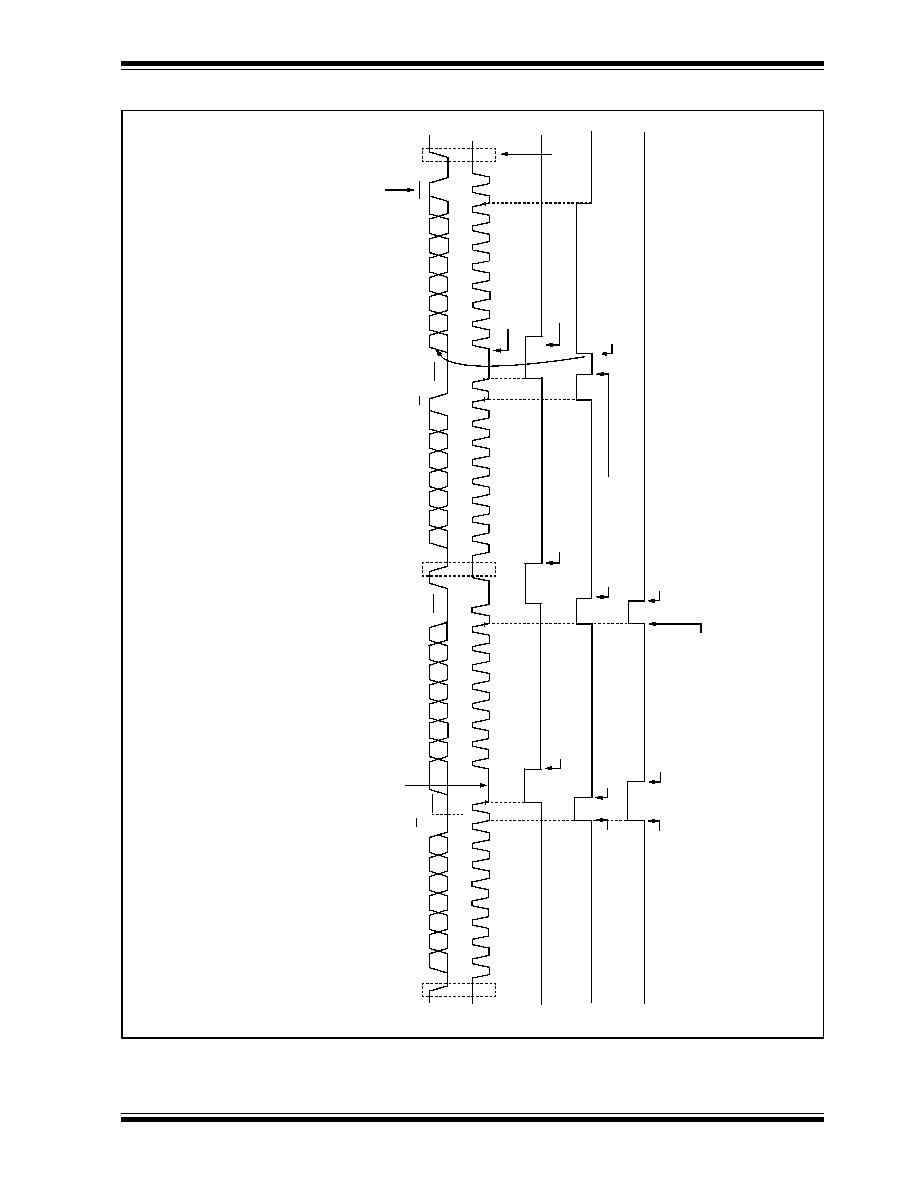
PIC18CXX2
©
7/99 Microchip Technology Inc.
Preliminary
DS39026B-page 131
FIGURE 14-10:
I
2
C SLAVE MODE WAVEFORM (TRANSMISSION 10-BIT ADDRESS)
SD
A
SCL
SSP
I
F
BF (
S
S
PST
A
T
<0
>)
S
1
2
3
4
56
7
8
9
1
23
4
5
6
7
89
1
2
3
4
5
7
8
9
P
1
1
11
0
A
9
A
8
A
7
A
6
A
5
A
4
A
3
A
2
A
1
A
0
1
11
1
0
A
8
R/W
=1
ACK
AC
K
R/W
= 0
AC
K
R
e
ceiv
e F
i
rst B
y
te o
f
A
ddre
s
s
Cle
a
r
e
d
in
so
f
t
wa
r
e
M
a
ster
sends
N
A
C
K
A9
6
(P
IR
1<
3>
)
R
e
ce
i
v
e
S
e
cond B
y
te
of A
ddre
s
s
C
l
e
a
red
by har
dw
are
w
hen
S
S
P
A
D
D
i
s
upda
ted.
U
A
(
S
S
P
ST
A
T
<1
>)
Clo
c
k is h
e
ld
lo
w u
n
t
il
up
date o
f
S
S
P
A
D
D
has
ta
k
en pl
ace
U
A
is se
t indicatin
g
that
the S
S
P
A
D
D
nee
ds to b
e
upda
ted
U
A
i
s
set
i
ndi
cati
ng
that
S
S
P
A
D
D
need
s to be
u
pdate
d
C
l
ear
ed b
y
hard
w
a
r
e w
h
e
n
S
S
P
A
D
D
i
s
upda
ted.
S
S
P
B
U
F
is wr
itte
n with
cont
ents of
S
S
P
S
R
D
u
mm
y read
of S
S
P
B
U
F
to cle
a
r B
F
f
l
a
g
R
e
cei
v
e
Fi
rst
B
y
te
of A
ddr
ess
12
3
4
5
7
8
9
D
7
D6
D5
D4
D3
D
1
AC
K
D2
6
T
r
ansm
i
tti
ng D
a
ta
B
y
t
e
D0
Du
m
m
y r
e
a
d
o
f
SSP
B
UF
to cle
a
r B
F
f
l
a
g
Sr
C
l
ea
red i
n
softw
are
W
r
i
t
e of
S
S
P
B
U
F
in
itia
te
s tr
a
n
s
m
i
t
C
l
ear
ed i
n
softw
are
T
r
ansmit
is comple
te
CK
P
h
a
s to be
set f
o
r
cl
o
c
k to be
relea
s
ed
B
u
s M
a
ster
te
r
m
ina
t
es
t
r
an
s
f
er
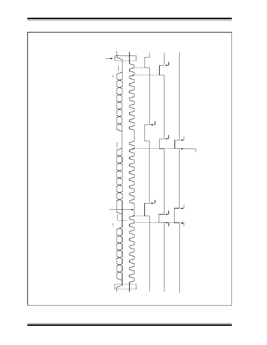
PIC18CXX2
DS39026B-page 132
Preliminary
©
7/99 Microchip Technology Inc.
FIGURE 14-11: I
2
C SLAVE MODE WAVEFORM (RECEPTION 10-BIT ADDRESS)
SD
A
SC
L
SS
P
I
F
BF
(
S
S
P
S
T
A
T
<0
>
)
S
1
2
3
4
56
7
8
9
1
23
4
5
6
7
89
1
2
3
4
5
7
8
9
P
1
1
1
1
0
A
9
A
8
A
7
A
6
A
5
A
4A
3A
2
A
1
A
0
D
7
D
6
D
5
D
4
D
3
D
1
D
0
Receiv
e Da
ta B
y
te
AC
K
R/W
= 0
ACK
R
e
ce
i
v
e F
i
rst B
y
te of
A
d
dress
C
l
ea
r
e
d i
n
s
o
f
t
w
a
r
e
B
u
s M
a
ster
te
r
m
i
n
at
e
s
tr
an
s
f
er
D2
6
(P
IR
1<
3>
)
R
e
cei
v
e
S
e
c
ond B
y
te o
f
A
d
dress
C
l
e
a
r
ed
by
ha
r
d
w
a
re
w
h
e
n
S
S
P
A
D
D
i
s
u
pdate
d
w
i
th
U
A
(
S
S
PST
A
T
<1
>)
C
l
oc
k i
s
he
l
d
l
o
w
unti
l
upd
ate of
S
S
P
A
D
D
ha
s
tak
e
n
pl
ace
U
A
i
s
set
i
n
di
cati
ng
that
t
he S
S
P
A
D
D
n
eeds to
be
u
pdate
d
U
A
is set ind
i
cating th
at
S
S
P
A
D
D
need
s to be
up
dated
SSP
B
UF
is wr
itte
n
with
con
t
ent
s
of S
S
P
S
R
Du
m
m
y
r
e
a
d
o
f
SSP
B
UF
to
cl
e
a
r B
F
flag
ACK
R/W
= 1
C
l
ear
ed i
n
so
ftw
a
r
e
Du
m
m
y r
e
a
d
o
f
SSP
B
UF
to cle
a
r B
F
f
l
a
g
R
ead of
S
S
P
B
U
F
cl
ear
s B
F
fl
ag
C
l
e
a
red
b
y
har
dw
are
w
hen
S
S
P
A
D
D
i
s
up
dated
w
i
th
l
o
w
b
y
te o
f
addr
ess
.
hi
gh b
y
t
e
of a
ddre
ss.
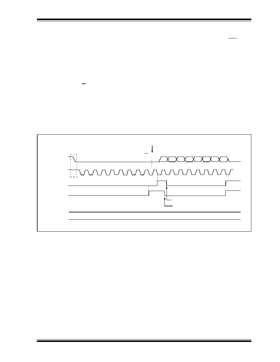
PIC18CXX2
©
7/99 Microchip Technology Inc.
Preliminary
DS39026B-page 133
14.3.2
GENERAL CALL ADDRESS SUPPORT
The addressing procedure for the I
2
C bus is such that
the first byte after the START condition usually deter-
mines which device will be the slave addressed by the
master. The exception is the general call address which
can address all devices. When this address is used, all
devices should, in theory, respond with an acknowl-
edge.
The general call address is one of eight addresses
reserved for specific purposes by the I
2
C protocol. It
consists of all 0's with R/W = 0.
The general call address is recognized when the Gen-
eral Call Enable bit (GCEN) is enabled (SSPCON2<7>
set). Following a start-bit detect, 8-bits are shifted into
the SSPSR and the address is compared against the
SSPADD. It is also compared to the general call
address and fixed in hardware.
If the general call address matches, the SSPSR is
transferred to the SSPBUF, the BF flag bit is set (eight
bit), and on the falling edge of the ninth bit (ACK bit), the
SSPIF interrupt flag bit is set.
When the interrupt is serviced, the source for the inter-
rupt can be checked by reading the contents of the
SSPBUF. The value can be used to determine if the
address was device specific or a general call address.
In 10-bit mode, the SSPADD is required to be updated
for the second half of the address to match, and the UA
bit is set (SSPSTAT<1>). If the general call address is
sampled when the GCEN bit is set, while the slave is
configured in 10-bit address mode, then the second
half of the address is not necessary, the UA bit will not
be set, and the slave will begin receiving data after the
acknowledge (Figure 14-12).
FIGURE 14-12: SLAVE MODE GENERAL CALL ADDRESS SEQUENCE (7 OR 10-BIT ADDRESS
MODE)
SDA
SCL
S
SSPIF
BF (SSPSTAT<0>)
SSPOV (SSPCON1<6>)
Cleared in software
SSPBUF is read
R/W = 0
ACK
General Call Address
Address is compared to General Call Address
GCEN (SSPCON2<7>)
Receiving data
ACK
1
2
3
4
5
6
7
8
9
1
2
3
4
5
6
7
8
9
D7
D6
D5
D4
D3
D2
D1
D0
after ACK, set interrupt
'0'
'1'
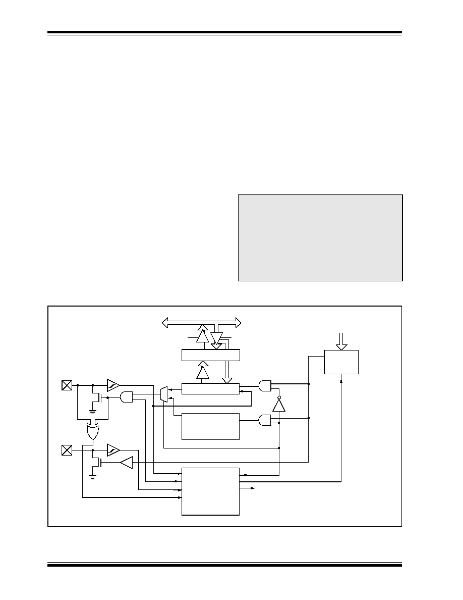
PIC18CXX2
DS39026B-page 134
Preliminary
©
7/99 Microchip Technology Inc.
14.3.3
MASTER MODE
Master mode of operation is supported by interrupt
generation on the detection of the START and STOP
conditions. The STOP (P) and START (S) bits are
cleared from a reset or when the MSSP module is dis-
abled. Control of the I
2
C bus may be taken when the P
bit is set or the bus is idle with both the S and P bits
clear.
In master mode, the SCL and SDA lines are manipu-
lated by the MSSP hardware.
The following events will cause SSP Interrupt Flag bit,
SSPIF, to be set (SSP Interrupt if enabled):
∑ START condition
∑ STOP condition
∑ Data transfer byte transmitted/received
∑ Acknowledge Transmit
∑ Repeated Start
14.3.4
I
2
C MASTER MODE SUPPORT
Master Mode is enabled by setting and clearing the
appropriate SSPM bits in SSPCON1 and by setting the
SSPEN bit. Once master mode is enabled, the user has
six options.
1.
Assert a start condition on SDA and SCL.
2.
Assert a Repeated Start condition on SDA and
SCL.
3.
Write to the SSPBUF register initiating transmis-
sion of data/address.
4.
Generate a stop Condition on SDA and SCL.
5.
Configure the I
2
C port to receive data.
6.
Generate an acknowledge condition at the end
of a received byte of data.
FIGURE 14-13: MSSP BLOCK DIAGRAM (I
2
C MASTER MODE)
Note:
The MSSP Module, when configured in I
2
C
Master Mode, does not allow queueing of
events. For instance, the user is not
allowed to initiate a start condition and
immediately write the SSPBUF register to
imitate transmission before the START
condition is complete. In this case, the
SSPBUF will not be written to and the
WCOL bit will be set, indicating that a write
to the SSPBUF did not occur.
Read
Write
SSPSR
Start bit, Stop bit,
Start bit detect
SSPBUF
Internal
Data Bus
Set/Reset, S, P, WCOL (SSPSTAT)
Shift
Clock
MSb
LSb
SDA
Acknowledge
Generate
Stop bit detect
Write collision detect
Clock Arbitration
State counter for
end of XMIT/RCV
SCL
SCL in
Bus Collision
SDA in
Rec
e
iv
e E
nab
le
cl
o
c
k cn
t
l
c
l
oc
k
ar
bi
t
r
at
e/
W
C
O
L
det
ect
(hold of
f
cloc
k
sourc
e
)
SSPADD<6:0>
Baud
Set SSPIF, BCLIF
Reset ACKSTAT, PEN (SSPCON2)
Rate
Generator
SSPM3:SSPM0

PIC18CXX2
©
7/99 Microchip Technology Inc.
Preliminary
DS39026B-page 135
14.3.4.1
I
2
C MASTER MODE OPERATION
The master device generates all of the serial clock
pulses and the START and STOP conditions. A trans-
fer is ended with a STOP condition or with a repeated
START condition. Since the repeated START condition
is also the beginning of the next serial transfer, the I
2
C
bus will not be released.
In Master transmitter mode serial data is output through
SDA, while SCL outputs the serial clock. The first byte
transmitted contains the slave address of the receiving
device (7 bits) and the Read/Write (R/W) bit. In this
case, the R/W bit will be logic '0'. Serial data is trans-
mitted 8 bits at a time. After each byte is transmitted, an
acknowledge bit is received. START and STOP condi-
tions are output to indicate the beginning and the end
of a serial transfer.
In Master receive mode, the first byte transmitted con-
tains the slave address of the transmitting device
(7 bits) and the R/W bit. In this case, the R/W bit will be
logic '1'. Thus, the first byte transmitted is a 7-bit slave
address followed by a '1' to indicate receive bit. Serial
data is received via SDA, while SCL outputs the serial
clock. Serial data is received 8 bits at a time. After each
byte is received, an acknowledge bit is transmitted.
START and STOP conditions indicate the beginning
and end of transmission.
The baud rate generator used for the SPI mode opera-
tion is now used to set the SCL clock frequency for
either 100 kHz, 400 kHz or 1 MHz I
2
C operation. The
baud rate generator reload value is contained in the
lower 7 bits of the SSPADD register. The baud rate gen-
erator will automatically begin counting on a write to the
SSPBUF. Once the given operation is complete, (i.e.
transmission of the last data bit is followed by ACK), the
internal clock will automatically stop counting and the
SCL pin will remain in its last state.
A typical transmit sequence would go as follows:
a)
The user generates a Start Condition by setting
the START enable bit SEN (SSPCON2<0>).
b)
SSPIF is set. The MSSP module will wait the
required start time before any other operation
takes place.
c)
The user loads the SSPBUF with the address to
transmit.
d)
Address is shifted out the SDA pin until all 8 bits
are transmitted.
e)
The MSSP Module shifts in the ACK bit from the
slave device and writes its value into the
SSPCON2 register (SSPCON2<6>).
f)
The MSSP module generates an interrupt at the
end of the ninth clock cycle by setting the SSPIF
bit.
g)
The user loads the SSPBUF with eight bits of
data.
h)
DATA is shifted out the SDA pin until all 8 bits are
transmitted.
i)
The MSSP Module shifts in the ACK bit from the
slave device and writes its value into the
SSPCON2 register (SSPCON2<6>).
j)
The MSSP module generates an interrupt at the
end of the ninth clock cycle by setting the SSPIF
bit.
k)
The user generates a STOP condition by setting
the STOP enable bit PEN (SSPCON2<2>).
l)
Interrupt is generated once the stop condition is
complete.
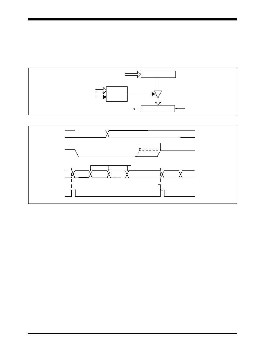
PIC18CXX2
DS39026B-page 136
Preliminary
©
7/99 Microchip Technology Inc.
14.3.5
BAUD RATE GENERATOR
In I
2
C master mode, the reload value for the BRG is
located in the lower 7 bits of the SSPADD register
(Figure 14-14). When the BRG is loaded with this
value, the BRG counts down to 0 and stops until
another reload has taken place. The BRG count is dec-
remented twice per instruction cycle (T
CY
) on the Q2
and Q4 clocks. In I
2
C master mode, the BRG is
reloaded automatically. If Clock Arbitration is taking
place for instance, the BRG will be reloaded when the
SCL pin is sampled high (Figure 14-15).
FIGURE 14-14: BAUD RATE GENERATOR BLOCK DIAGRAM
FIGURE 14-15: BAUD RATE GENERATOR TIMING WITH CLOCK ARBITRATION
SSPM3:SSPM0
BRG Down Counter
CLKOUT
Fosc/4
SSPADD<6:0>
SSPM3:SSPM0
SCL
Reload
Control
Reload
SDA
SCL
SCL de-asserted but slave holds
DX-1
DX
BRG
SCL is sampled high, reload takes
place and BRG starts its count.
03h
02h
01h
00h (hold off)
03h
02h
reload
BRG
value
SCL low (clock arbitration)
SCL allowed to transition high
BRG decrements on
Q2 and Q4 cycles
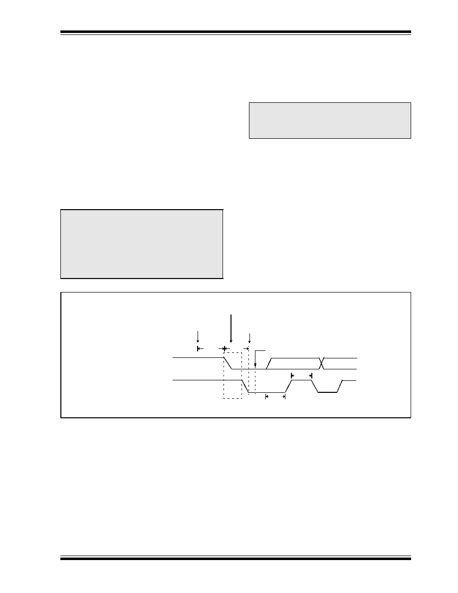
PIC18CXX2
©
7/99 Microchip Technology Inc.
Preliminary
DS39026B-page 137
14.3.6
I
2
C MASTER MODE START CONDITION
TIMING
To initiate a START condition, the user sets the start
condition enable bit SEN (SSPCON2<0>). If the SDA
and SCL pins are sampled high, the baud rate genera-
tor is re-loaded with the contents of SSPADD<6:0> and
starts its count. If SCL and SDA are both sampled high
when the baud rate generator times out (T
BRG
), the
SDA pin is driven low. The action of the SDA being
driven low, while SCL is high, is the START condition,
and causes the S bit (SSPSTAT<3>) to be set. Follow-
ing this, the baud rate generator is reloaded with the
contents of SSPADD<6:0> and resumes its count.
When the baud rate generator times out (T
BRG
), the
SEN bit (SSPCON2<0>) will be automatically cleared
by hardware, the baud rate generator is suspended
leaving the SDA line held low and the START condition
is complete.
14.3.6.1
WCOL STATUS FLAG
If the user writes the SSPBUF when an START
sequence is in progress, the WCOL is set and the con-
tents of the buffer are unchanged (the write doesn't
occur).
FIGURE 14-16: FIRST START BIT TIMING
Note:
If at the beginning of the START condition,
the SDA and SCL pins are already sam-
pled low, or if during the START condition
the SCL line is sampled low before the SDA
line is driven low, a bus collision occurs, the
Bus Collision Interrupt Flag BCLIF is set,
the START condition is aborted, and the
I
2
C module is reset into its IDLE state.
Note:
Because queueing of events is not
allowed, writing to the lower 5 bits of
SSPCON2 is disabled until the START
condition is complete.
SDA
SCL
S
T
BRG
1st Bit
2nd Bit
T
BRG
SDA = 1,
At completion of start bit,
SCL = 1
Write to SSPBUF occurs here
T
BRG
Hardware clears SEN bit
T
BRG
Write to SEN bit occurs here.
Set S bit (SSPSTAT<3>)
and sets SSPIF bit
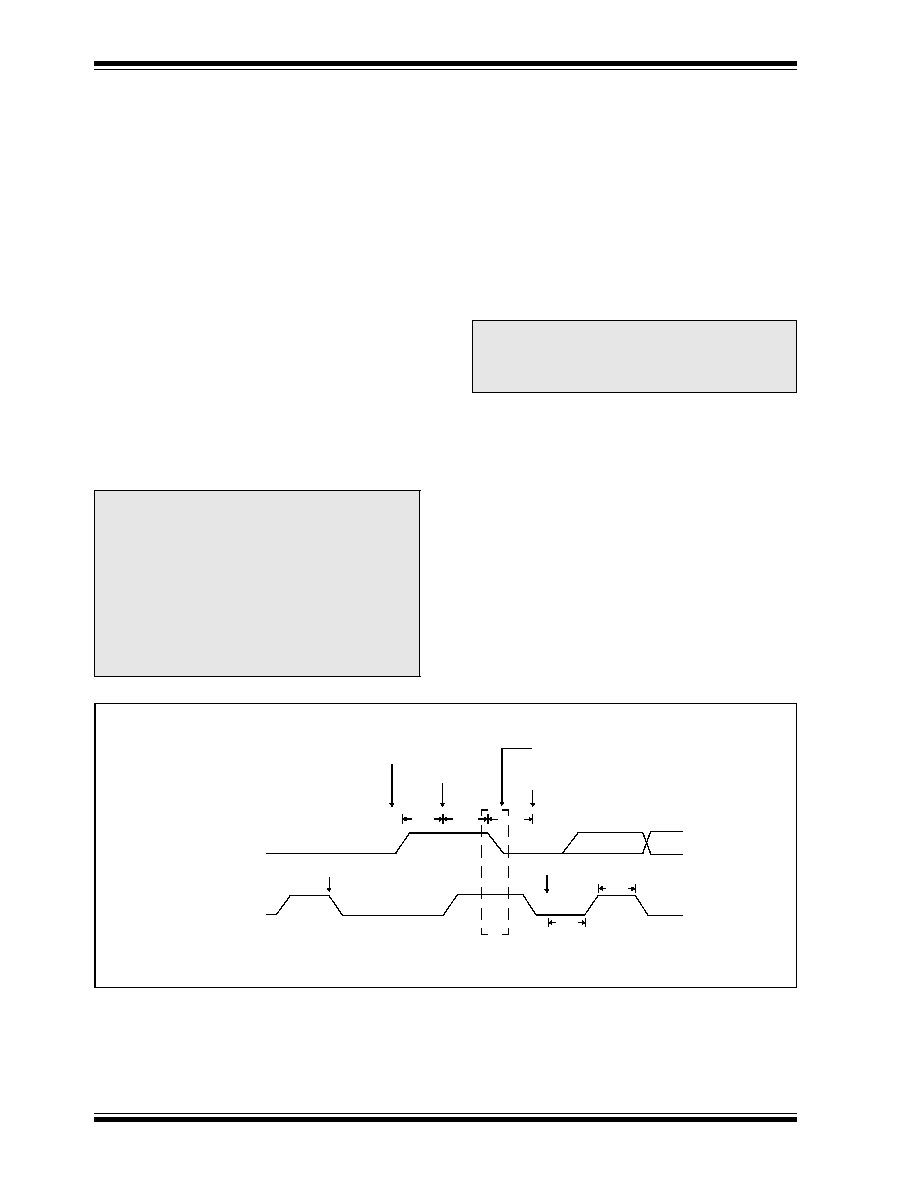
PIC18CXX2
DS39026B-page 138
Preliminary
©
7/99 Microchip Technology Inc.
14.3.7
I
2
C MASTER MODE REPEATED START
CONDITION TIMING
A Repeated Start condition occurs when the RSEN bit
(SSPCON2<1>) is programmed high and the I
2
C logic
module is in the idle state. When the RSEN bit is set,
the SCL pin is asserted low. When the SCL pin is sam-
pled low, the baud rate generator is loaded with the
contents of SSPADD<5:0> and begins counting. The
SDA pin is released (brought high) for one baud rate
generator count (T
BRG
). When the baud rate generator
times out, if SDA is sampled high, the SCL pin will be
de-asserted (brought high). When SCL is sampled
high, the baud rate generator is re-loaded with the con-
tents of SSPADD<6:0> and begins counting. SDA and
SCL must be sampled high for one T
BRG
. This action is
then followed by assertion of the SDA pin (SDA = 0) for
one T
BRG,
while SCL is high. Following this, the RSEN
bit (SSPCON2<1>) will be automatically cleared and
the baud rate generator will not be reloaded, leaving
the SDA pin held low. As soon as a start condition is
detected on the SDA and SCL pins, the S bit (SSP-
STAT<3>) will be set. The SSPIF bit will not be set until
the baud rate generator has timed-out.
Immediately following the SSPIF bit getting set, the
user may write the SSPBUF with the 7-bit address in
7-bit mode, or the default first address in 10-bit mode.
After the first eight bits are transmitted and an ACK is
received, the user may then transmit an additional
eight bits of address (10-bit mode) or eight bits of data
(7-bit mode).
14.3.7.1
WCOL STATUS FLAG
If the user writes the SSPBUF when a Repeated Start
sequence is in progress, the WCOL is set and the con-
tents of the buffer are unchanged (the write doesn't
occur).
FIGURE 14-17: REPEAT START CONDITION WAVEFORM
Note 1: If RSEN is programmed while any other
event is in progress, it will not take effect.
Note 2: A bus collision during the Repeated Start
condition occurs if:
∑ SDA is sampled low when SCL goes
from low to high.
∑ SCL goes low before SDA is
asserted low. This may indicate that
another master is attempting to
transmit a data "1".
Note:
Because queueing of events is not
allowed, writing of the lower 5 bits of
SSPCON2 is disabled until the Repeated
Start condition is complete.
SDA
SCL
Sr = Repeated Start
Write to SSPCON2
Write to SSPBUF occurs here.
Falling edge of ninth clock
End of Xmit
At completion of start bit,
hardware clear RSEN bit
1st Bit
Set S (SSPSTAT<3>)
T
BRG
T
BRG
SDA = 1,
SDA = 1,
SCL(no change)
SCL = 1
occurs here.
T
BRG
T
BRG
T
BRG
and set SSPIF

PIC18CXX2
©
7/99 Microchip Technology Inc.
Preliminary
DS39026B-page 139
14.3.8
I
2
C MASTER MODE TRANSMISSION
Transmission of a data byte, a 7-bit address or the other
half of a 10-bit address is accomplished by simply writ-
ing a value to the SSPBUF register. This action will set
the buffer full flag bit, BF, and allow the baud rate gen-
erator to begin counting and start the next transmis-
sion. Each bit of address/data will be shifted out onto
the SDA pin after the falling edge of SCL is asserted
(see data hold time specification
parameter 106
). SCL
is held low for one baud rate generator roll over count
(T
BRG
). Data should be valid before SCL is released
high (see Data setup time specification
parameter
107
). When the SCL pin is released high, it is held that
way for T
BRG
. The data on the SDA pin must remain
stable for that duration and some hold time after the
next falling edge of SCL. After the eighth bit is shifted
out (the falling edge of the eighth clock), the BF flag is
cleared and the master releases SDA. allowing the
slave device being addressed to respond with an ACK
bit during the ninth bit time, if an address match occurs
or if data was received properly. The status of ACK is
written into the ACKDT bit on the falling edge of the
ninth clock. If the master receives an acknowledge, the
acknowledge status bit, ACKSTAT, is cleared. If not, the
bit is set. After the ninth clock, the SSPIF bit is set and
the master clock (baud rate generator) is suspended
until the next data byte is loaded into the SSPBUF, leav-
ing SCL low and SDA unchanged (Figure 14-18).
After the write to the SSPBUF, each bit of address will
be shifted out on the falling edge of SCL until all seven
address bits and the R/W bit are completed. On the fall-
ing edge of the eighth clock, the master will de-assert
the SDA pin allowing the slave to respond with an
acknowledge. On the falling edge of the ninth clock, the
master will sample the SDA pin to see if the address
was recognized by a slave. The status of the ACK bit is
loaded into the ACKSTAT status bit (SSPCON2<6>).
Following the falling edge of the ninth clock transmis-
sion of the address, the SSPIF is set, the BF flag is
cleared and the baud rate generator is turned off until
another write to the SSPBUF takes place, holding SCL
low and allowing SDA to float.
14.3.8.1
BF STATUS FLAG
In transmit mode, the BF bit (SSPSTAT<0>) is set when
the CPU writes to SSPBUF and is cleared when all 8
bits are shifted out.
14.3.8.2
WCOL STATUS FLAG
If the user writes the SSPBUF when a transmit is
already in progress, (i.e. SSPSR is still shifting out a
data byte), the WCOL is set and the contents of the
buffer are unchanged (the write doesn't occur).
WCOL must be cleared in software.
14.3.8.3
ACKSTAT STATUS FLAG
In transmit mode, the ACKSTAT bit (SSPCON2<6>) is
cleared when the slave has sent an acknowledge
(ACK = 0), and is set when the slave does not acknowl-
edge (ACK = 1). A slave sends an acknowledge when
it has recognized its address (including a general call)
or when the slave has properly received its data.
14.3.9
I
2
C MASTER MODE RECEPTION
Master mode reception is enabled by programming the
receive enable bit, RCEN (SSPCON2<3>).
The baud rate generator begins counting, and on each
rollover, the state of the SCL pin changes (high to low/
low to high) and data is shifted into the SSPSR. After
the falling edge of the eighth clock, the receive enable
flag is automatically cleared, the contents of the
SSPSR are loaded into the SSPBUF, the BF flag bit is
set, the SSPIF flag bit is set and the baud rate genera-
tor is suspended from counting, holding SCL low. The
MSSP is now in IDLE state, awaiting the next com-
mand. When the buffer is read by the CPU, the BF flag
bit is automatically cleared. The user can then send an
acknowledge bit at the end of reception, by setting the
acknowledge sequence enable bit ACKEN
(SSPCON2<4>).
14.3.9.1
BF STATUS FLAG
In receive operation, the BF bit is set when an address
or data byte is loaded into SSPBUF from SSPSR. It is
cleared when the SSPBUF register is read.
14.3.9.2
SSPOV STATUS FLAG
In receive operation, the SSPOV bit is set when 8 bits
are received into the SSPSR and the BF flag bit is
already set from a previous reception.
14.3.9.3
WCOL STATUS FLAG
If the user writes the SSPBUF when a receive is
already in progress (i.e. SSPSR is still shifting in a data
byte), the the WCOL bit is set and the contents of the
buffer are unchanged (the write doesn't occur).
Note:
The MSSP Module must be in an IDLE
STATE before the RCEN bit is set, or the
RCEN bit will be disregarded.
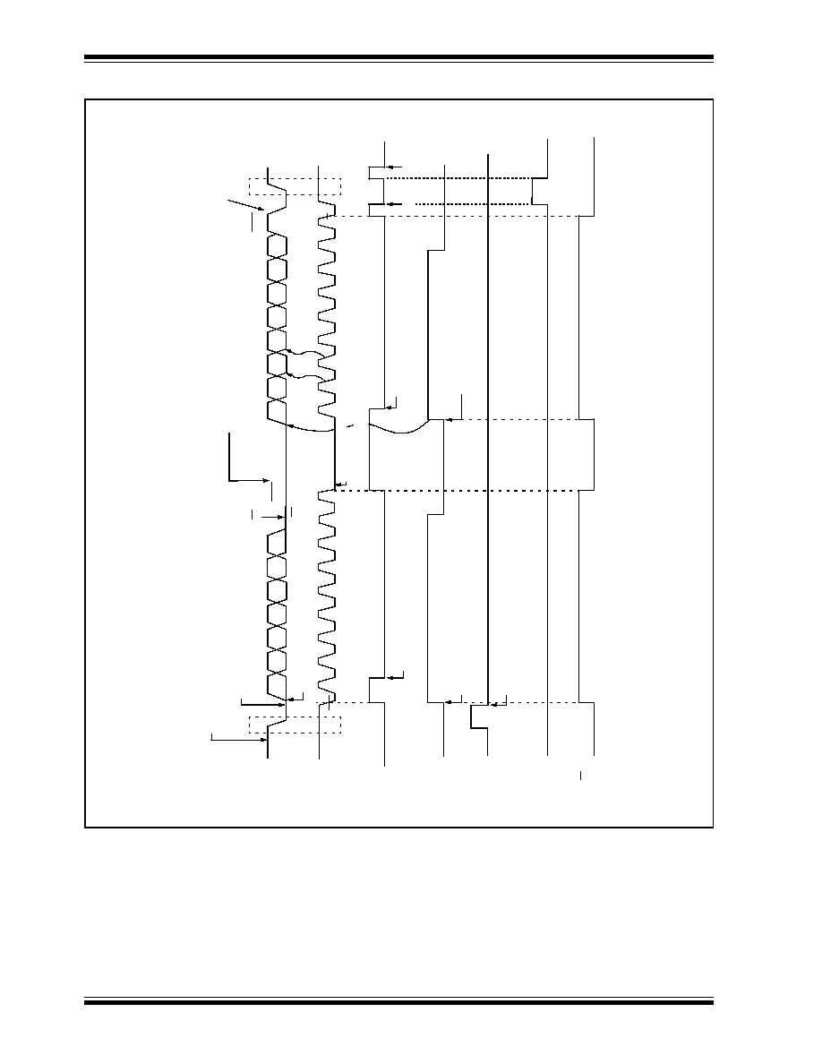
PIC18CXX2
DS39026B-page 140
Preliminary
©
7/99 Microchip Technology Inc.
FIGURE 14-18: I
2
C MASTER MODE WAVEFORM (TRANSMISSION, 7 OR 10-BIT ADDRESS)
SD
A
SC
L
S
SPI
F
B
F
(
S
SPST
A
T
<0
>)
SE
N
A7
A
6
A5
A4
A
3
A
2
A1
A
C
K
=
0
D
7
D
6
D
5D
4
D
3D
2
D
1D
0
ACK
T
r
a
n
sm
i
t
ting
Data or
S
e
co
nd
Half
R/
W
= 0
T
r
an
smi
t
A
d
dr
ess
t
o
S
l
ave
1
2
3
4
5
6789
12
3
4
5
6
7
8
9
P
cle
a
r
e
d
in
so
ft
wa
r
e
se
r
v
ice
r
o
u
t
in
e
SSPBUF
is
wr
it
t
e
n
in
s
o
f
t
w
a
r
e
Fr
o
m
SSP in
t
e
r
r
u
p
t
A
f
t
e
r
st
ar
t co
ndi
t
i
o
n
S
E
N
c
l
e
a
r
ed
by h
a
rd
w
a
r
e
.
S
SSPBUF
wr
it
t
e
n
wit
h
7
b
i
t
a
d
d
r
e
s
s
a
n
d
R/
W
star
t tr
ansm
i
t
SCL
h
e
ld
lo
w
wh
i
l
e
CPU
r
e
s
p
o
n
d
s
t
o
SSPI
F
SEN = 0
of
1
0
-
b
i
t
A
d
dr
e
s
s
W
r
it
e
SSPCO
N
2
<
0
>
SEN = 1
S
T
A
R
T c
o
n
d
i
ti
on
be
gi
ns
F
r
o
m
sl
a
v
e c
l
e
a
r
A
C
K
S
T
A
T
bi
t
S
S
P
C
O
N
2<
6>
ACKST
A
T
in
SSPCO
N
2
= 1
cl
ear
ed
i
n
so
ftw
a
r
e
SS
PBUF wr
it
t
e
n
PE
N
Cle
a
r
e
d
in
so
ft
wa
r
e
R/W
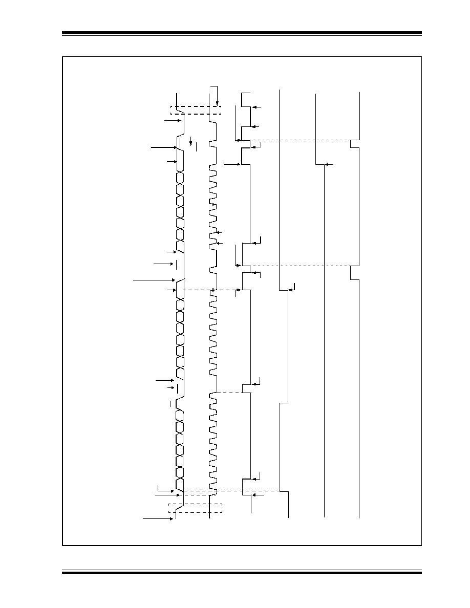
PIC18CXX2
©
7/99 Microchip Technology Inc.
Preliminary
DS39026B-page 141
FIGURE 14-19: I
2
C MASTER MODE WAVEFORM (RECEPTION, 7-BIT ADDRESS)
P
9
8
7
6
5
D0
D1
D2
D3
D4
D5
D6
D7
S
A7
A6
A5
A4
A3
A2
A1
SDA
SCL
12
3
4
5
6
7
8
9
12
3
4
5
67
8
9
12
3
4
B
u
s M
a
ste
r
ter
m
in
ate
s
t
r
an
s
f
er
ACK
Re
ce
ivin
g
Da
t
a
fr
o
m
Sla
v
e
Re
ce
ivin
g
Da
t
a
fr
o
m
S
l
a
v
e
D0
D1
D2
D3
D4
D5
D6
D7
AC
K
R/W
= 1
T
r
ansm
i
t
A
d
dress t
o
S
l
a
v
e
SSP
I
F
BF
AC
K
is n
o
t sent
W
r
i
t
e
to
SSP
CON2
<0
>
(
S
E
N = 1
)
Wr
it
e
t
o
SSP
BUF
o
c
c
u
r
s
h
e
r
e
A
C
K f
r
o
m
Sla
v
e
Mast
er con
f
i
gur
ed as a
recei
v
e
r
by pr
ogr
amm
i
n
g
S
S
P
C
ON
2<
3>
, (
R
C
E
N
=
1)
PEN b
i
t
= 1
w
r
i
t
ten he
re
D
a
ta
shi
fted
i
n
on fa
l
l
i
n
g edg
e of C
L
K
Cle
a
r
e
d
in
so
ftwa
r
e
S
t
ar
t X
M
IT
SE
N
=
0
S
SPO
V
SD
A
=
0
,
SC
L
=
1
wh
ile
CPU
(
SSPST
A
T
<0
>)
ACK
Last bi
t i
s
shi
fted i
n
to S
S
P
S
R
and
content
s a
r
e u
n
l
oaded
i
n
to S
S
P
B
U
F
C
l
ear
ed i
n
so
ftw
are
C
l
ear
ed i
n
so
ftw
are
Se
t
SS
PI
F in
t
e
r
r
u
p
t
at e
nd of
recei
v
e
Se
t
P
b
i
t
(
S
SP
S
T
A
T
<4
>)
a
nd S
S
P
IF
C
l
ea
r
e
d i
n
software
A
C
K
fr
om M
a
ster
Se
t
SSP
I
F
a
t
e
n
d
S
e
t S
S
P
I
F
in
terr
upt
at en
d of ack
now
l
edge
seque
nce
Se
t
SSP
I
F
in
t
e
r
r
u
p
t
a
t
end o
f
ackno
w
-
l
e
d
ge seq
uence
o
f
r
e
ce
i
v
e
S
e
t
A
C
K
E
N
sta
r
t ackn
ow
l
edge
seque
nce
SS
PO
V is
s
e
t
b
e
c
a
u
s
e
SS
PBUF
is still fu
ll
SDA
= ACKDT
= 1
RCE
N cle
a
r
e
d
auto
m
ati
c
al
l
y
R
C
E
N
=
1 st
ar
t
next r
e
cei
v
e
W
r
ite
to S
S
P
C
ON2<
4>
to
st
art a
cknow
l
edge
seque
nce
SDA =
A
C
KDT
(
S
SPCO
N
2
<
5
>
)
= 0
RCE
N cle
a
r
e
d
auto
m
ati
c
al
l
y
resp
onds to
S
S
P
I
F
A
C
KEN
B
e
g
i
n
S
t
art C
o
ndi
ti
on
Cle
a
r
e
d
in
so
ftwa
r
e
S
D
A = ACK
D
T = 0
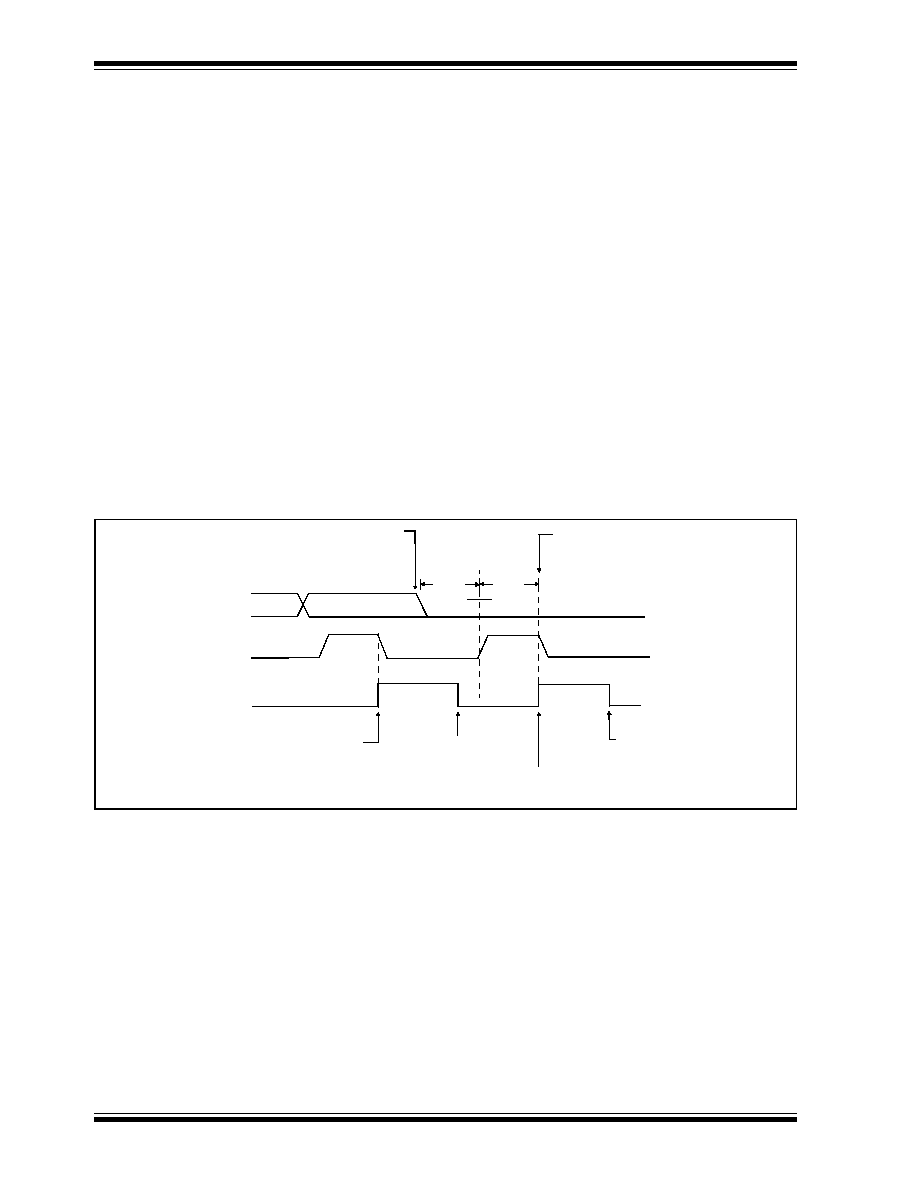
PIC18CXX2
DS39026B-page 142
Preliminary
©
7/99 Microchip Technology Inc.
14.3.10 ACKNOWLEDGE SEQUENCE TIMING
An acknowledge sequence is enabled by setting the
acknowledge sequence enable bit ACKEN
(SSPCON2<4>). When this bit is set, the SCL pin is
pulled low and the contents of the acknowledge data bit
is presented on the SDA pin. If the user wishes to gen-
erate an acknowledge, then the ACKDT bit should be
cleared. If not, the user should set the ACKDT bit
before starting an acknowledge sequence. The baud
rate generator then counts for one rollover period
(T
BRG
) and the SCL pin is de-asserted (pulled high).
When the SCL pin is sampled high (clock arbitration),
the baud rate generator counts for T
BRG
. The SCL pin
is then pulled low. Following this, the ACKEN bit is auto-
matically cleared, the baud rate generator is turned off
and the MSSP module then goes into IDLE mode
(Figure 14-20).
14.3.10.1 WCOL STATUS FLAG
If the user writes the SSPBUF when an acknowledge
sequence is in progress, then WCOL is set and the
contents of the buffer are unchanged (the write doesn't
occur).
14.3.11 STOP CONDITION TIMING
A stop bit is asserted on the SDA pin at the end of a
receive/transmit by setting the Stop sequence enable
bit, PEN (SSPCON2<2>). At the end of a receive/trans-
mit the SCL line is held low after the falling edge of the
ninth clock. When the PEN bit is set, the master will
assert the SDA line low. When the SDA line is sampled
low, the baud rate generator is reloaded and counts
down to 0. When the baud rate generator times out, the
SCL pin will be brought high, and one T
BRG
(baud rate
generator rollover count) later, the SDA pin will be de-
asserted. When the SDA pin is sampled high while SCL
is high, the P bit (SSPSTAT<4>) is set. A T
BRG
later, the
PEN bit is cleared and the SSPIF bit is set (Figure 14-
21).
14.3.11.1 WCOL STATUS FLAG
If the user writes the SSPBUF when a STOP sequence
is in progress, then the WCOL bit is set and the con-
tents of the buffer are unchanged (the write doesn't
occur).
FIGURE 14-20: ACKNOWLEDGE SEQUENCE WAVEFORM
Note: T
BRG
= one baud rate generator period.
SDA
SCL
Set SSPIF at the end
Acknowledge sequence starts here,
Write to SSPCON2
ACKEN automatically cleared
Cleared in
T
BRG
T
BRG
of receive
ACK
8
ACKEN = 1, ACKDT = 0
D0
9
SSPIF
software
Set SSPIF at the end
of acknowledge sequence
Cleared in
software
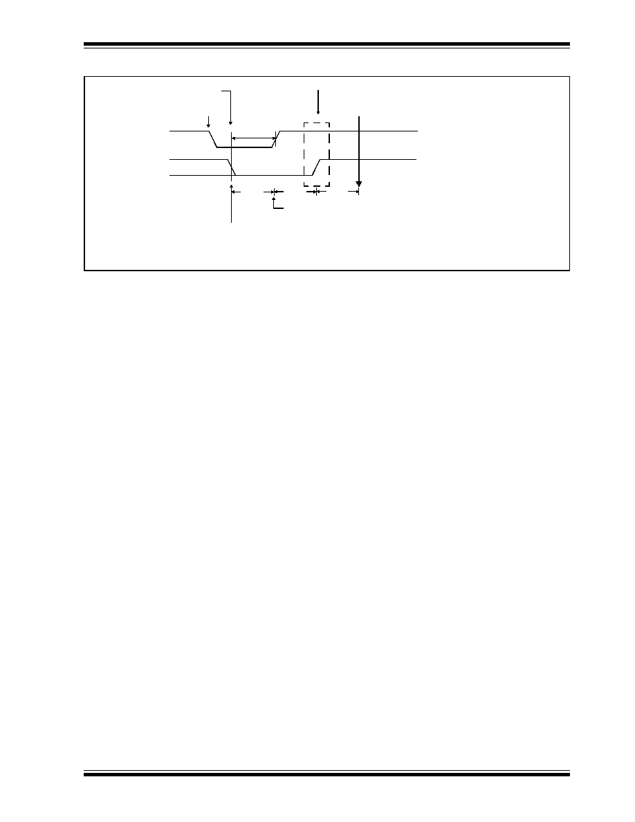
PIC18CXX2
©
7/99 Microchip Technology Inc.
Preliminary
DS39026B-page 143
FIGURE 14-21: STOP CONDITION RECEIVE OR TRANSMIT MODE
SCL
SDA
SDA asserted low before rising edge of clock
Write to SSPCON2
Set PEN
Falling edge of
SCL = 1 for Tbrg, followed by SDA = 1 for Tbrg
9th clock
SCL brought high after T
BRG
Note: T
BRG
= one baud rate generator period.
T
BRG
T
BRG
after SDA sampled high. P bit (SSPSTAT<4>) is set
T
BRG
to setup stop condition
.
ACK
P
T
BRG
PEN bit (SSPCON2<2>) is cleared by
hardware and the SSPIF bit is set
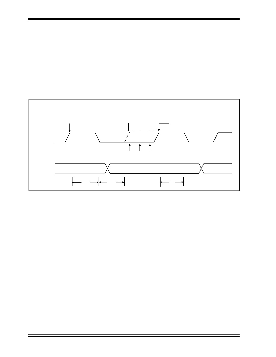
PIC18CXX2
DS39026B-page 144
Preliminary
©
7/99 Microchip Technology Inc.
14.3.12 CLOCK ARBITRATION
Clock arbitration occurs when the master, during any
receive, transmit or repeated start/stop condition, de-
asserts the SCL pin (SCL allowed to float high). When
the SCL pin is allowed to float high, the baud rate gen-
erator (BRG) is suspended from counting until the SCL
pin is actually sampled high. When the SCL pin is sam-
pled high, the baud rate generator is reloaded with the
contents of SSPADD<6:0> and begins counting. This
ensures that the SCL high time will always be at least
one BRG rollover count in the event that the clock is
held low by an external device (Figure 14-22).
14.3.13 SLEEP OPERATION
While in sleep mode, the I
2
C module can receive
addresses or data, and when an address match or
complete byte transfer occurs, wake the processor from
sleep (if the MSSP interrupt is enabled).
14.3.14 EFFECT OF A RESET
A reset disables the MSSP module and terminates the
current transfer.
FIGURE 14-22: CLOCK ARBITRATION TIMING IN MASTER TRANSMIT MODE
SCL
SDA
BRG overflow,
Release SCL,
If SCL = 1 Load BRG with
SSPADD<6:0>, and start count
BRG overflow occurs,
Release SCL, Slave device holds SCL low.
SCL = 1 BRG starts counting
clock high interval.
SCL line sampled once every machine cycle (T
OSC
≤ 4).
Hold off BRG until SCL is sampled high.
T
BRG
T
BRG
T
BRG
to measure high time interval
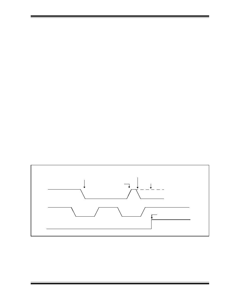
PIC18CXX2
©
7/99 Microchip Technology Inc.
Preliminary
DS39026B-page 145
14.3.15 MULTI-MASTER MODE
In multi-master mode, the interrupt generation on the
detection of the START and STOP conditions allows
the determination of when the bus is free. The STOP
(P) and START (S) bits are cleared from a reset or
when the MSSP module is disabled. Control of the I
2
C
bus may be taken when the P bit (SSPSTAT<4>) is set,
or the bus is idle with both the S and P bits clear. When
the bus is busy, enabling the SSP Interrupt will gener-
ate the interrupt when the STOP condition occurs.
In multi-master operation, the SDA line must be moni-
tored, for arbitration, to see if the signal level is the
expected output level. This check is performed in hard-
ware, with the result placed in the BCLIF bit.
The states where arbitration can be lost are:
∑ Address Transfer
∑ Data Transfer
∑ A Start Condition
∑ A Repeated Start Condition
∑ An Acknowledge Condition
14.3.16 MULTI -MASTER COMMUNICATION, BUS
COLLISION, AND BUS ARBITRATION
Multi-Master mode support is achieved by bus arbitra-
tion. When the master outputs address/data bits onto
the SDA pin, arbitration takes place when the master
outputs a '1' on SDA by letting SDA float high and
another master asserts a '0'. When the SCL pin floats
high, data should be stable. If the expected data on
SDA is a '1' and the data sampled on the SDA pin = '0',
then a bus collision has taken place. The master will set
the Bus Collision Interrupt Flag BCLIF and reset the I
2
C
port to its IDLE state. (Figure 14-23).
If a transmit was in progress when the bus collision
occurred, the transmission is halted, the BF flag is
cleared, the SDA and SCL lines are de-asserted, and
the SSPBUF can be written to. When the user services
the bus collision interrupt service routine, and if the I
2
C
bus is free, the user can resume communication by
asserting a START condition.
If a START, Repeated Start, STOP, or Acknowledge
condition was in progress when the bus collision
occurred, the condition is aborted, the SDA and SCL
lines are de-asserted, and the respective control bits in
the SSPCON2 register are cleared. When the user ser-
vices the bus collision interrupt service routine, and if
the I
2
C bus is free, the user can resume communication
by asserting a START condition.
The Master will continue to monitor the SDA and SCL
pins. If a STOP condition occurs, the SSPIF bit will be
set.
A write to the SSPBUF will start the transmission of
data at the first data bit, regardless of where the trans-
mitter left off when the bus collision occurred.
In multi-master mode, the interrupt generation on the
detection of start and stop conditions allows the deter-
mination of when the bus is free. Control of the I
2
C bus
can be taken when the P bit is set in the SSPSTAT reg-
ister, or the bus is idle and the S and P bits are cleared.
FIGURE 14-23: BUS COLLISION TIMING FOR TRANSMIT AND ACKNOWLEDGE
SDA
SCL
BCLIF
SDA released
SDA line pulled low
by another source
Sample SDA. While SCL is high
data doesn't match what is driven
Bus collision has occurred.
Set bus collision
interrupt (BCLIF).
by the master.
by master
Data changes
while SCL = 0
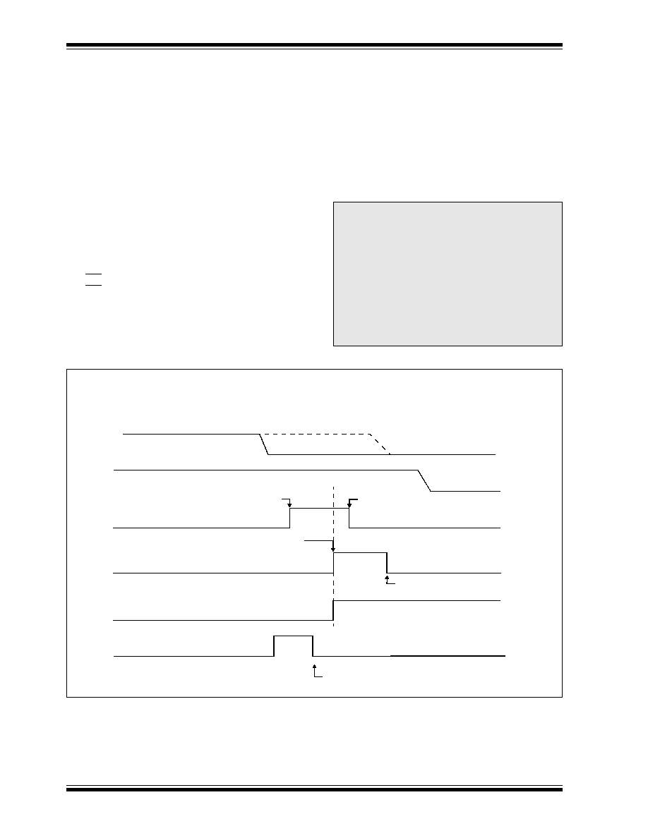
PIC18CXX2
DS39026B-page 146
Preliminary
©
7/99 Microchip Technology Inc.
14.3.16.1 BUS COLLISION DURING A START
CONDITION
During a START condition, a bus collision occurs if:
a)
SDA or SCL are sampled low at the beginning of
the START condition (Figure 14-24).
b)
SCL is sampled low before SDA is asserted low
(Figure 14-25).
During a START condition, both the SDA and the SCL
pins are monitored.
If:
the SDA pin is already low
or the SCL pin is already low,
then:
the START condition is aborted,
and the BCLIF flag is set,
and the MSSP module is reset to its IDLE state
(Figure 14-24).
The START condition begins with the SDA and SCL
pins de-asserted. When the SDA pin is sampled high,
the baud rate generator is loaded from SSPADD<6:0>
and counts down to 0. If the SCL pin is sampled low
while SDA is high, a bus collision occurs, because it is
assumed that another master is attempting to drive a
data '1' during the START condition.
If the SDA pin is sampled low during this count, the
BRG is reset and the SDA line is asserted early
(Figure 14-26). If however a '1' is sampled on the SDA
pin, the SDA pin is asserted low at the end of the BRG
count. The baud rate generator is then reloaded and
counts down to 0, and during this time, if the SCL pins
is sampled as '0', a bus collision does not occur. At the
end of the BRG count, the SCL pin is asserted low.
FIGURE 14-24: BUS COLLISION DURING START CONDITION (SDA ONLY)
Note:
The reason that bus collision is not a factor
during a START condition is that no two
bus masters can assert a START condition
at the exact same time. Therefore, one
master will always assert SDA before the
other. This condition does not cause a bus
collision, because the two masters must be
allowed to arbitrate the first address follow-
ing the START condition. If the address is
the same, arbitration must be allowed to
continue into the data portion, Repeated
Start or STOP conditions.
SDA
SCL
SEN
SDA sampled low before
SDA goes low before the SEN bit is set.
S bit and SSPIF set because
SSP module reset into idle state.
SEN cleared automatically because of bus collision.
S bit and SSPIF set because
Set SEN, enable start
condition if SDA = 1, SCL=1
SDA = 0, SCL = 1
BCLIF
S
SSPIF
SDA = 0, SCL = 1
SSPIF and BCLIF are
cleared in software.
SSPIF and BCLIF are
cleared in software.
. Set BCLIF,
Set BCLIF.
START condition.
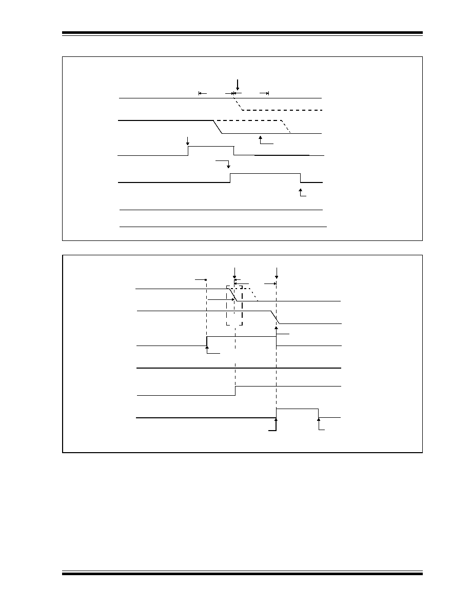
PIC18CXX2
©
7/99 Microchip Technology Inc.
Preliminary
DS39026B-page 147
FIGURE 14-25: BUS COLLISION DURING START CONDITION (SCL = 0)
FIGURE 14-26: BRG RESET DUE TO SDA ARBITRATION DURING START CONDITION
SDA
SCL
SEN
Bus collision occurs, Set BCLIF.
SCL = 0 before SDA = 0,
Set SEN, enable start
sequence if SDA = 1, SCL = 1
T
BRG
T
BRG
SDA = 0, SCL = 1
BCLIF
S
SSPIF
Interrupt cleared
in software.
Bus collision occurs, Set BCLIF.
SCL = 0 before BRG time out,
'0'
'0'
'0'
'0'
SDA
SCL
SEN
Set S
Set SEN, enable start
sequence if SDA = 1, SCL = 1
Less than T
BRG
T
BRG
SDA = 0, SCL = 1
BCLIF
S
SSPIF
S
Interrupts cleared
in software.
Set SSPIF
SDA = 0, SCL = 1
SDA pulled low by other master.
Reset BRG and assert SDA
SCL pulled low after BRG
Timeout
Set SSPIF
'0'
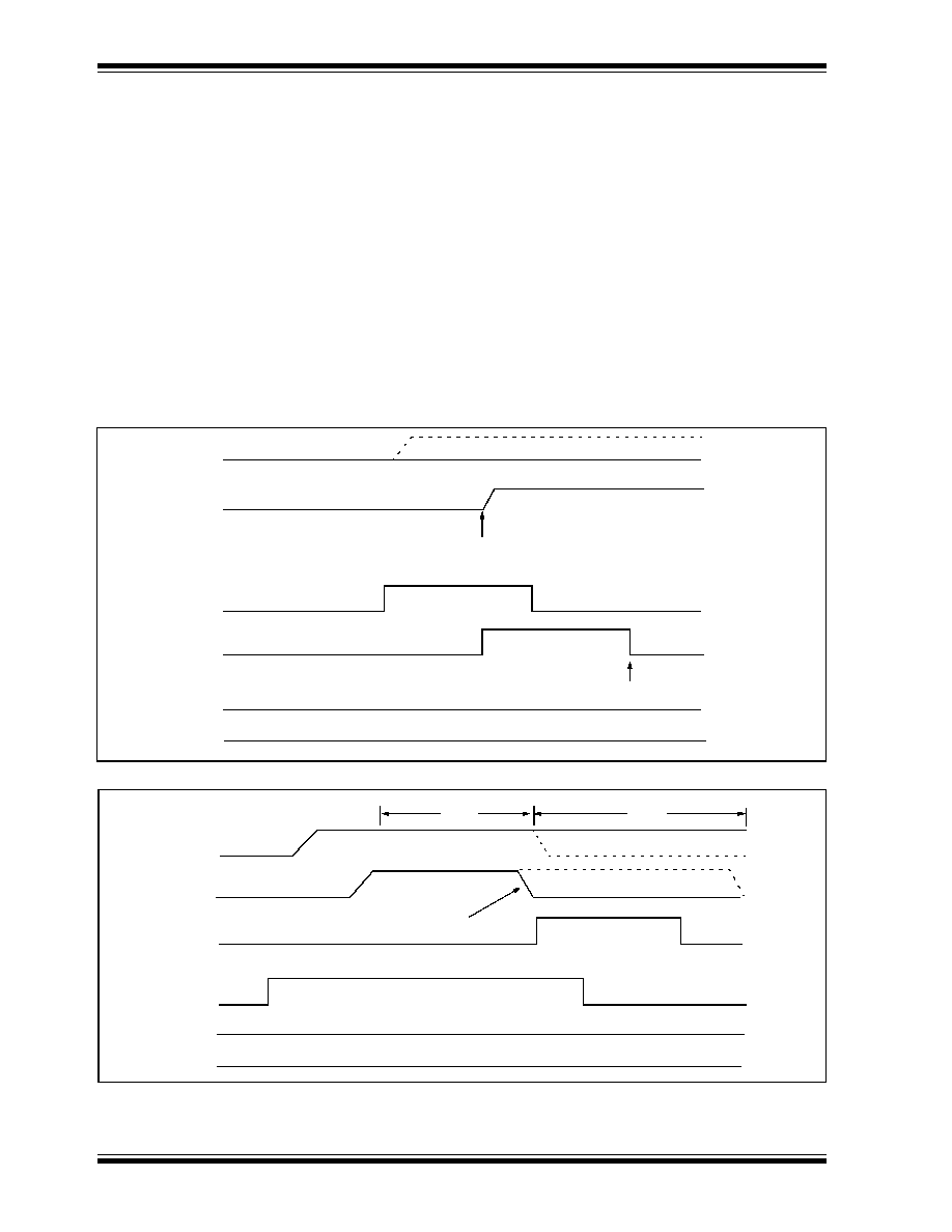
PIC18CXX2
DS39026B-page 148
Preliminary
©
7/99 Microchip Technology Inc.
14.3.16.2 BUS COLLISION DURING A REPEATED
START CONDITION
During a Repeated Start condition, a bus collision
occurs if:
a)
A low level is sampled on SDA when SCL goes
from low level to high level.
b)
SCL goes low before SDA is asserted low, indi-
cating that another master is attempting to trans-
mit a data '1'.
When the user de-asserts SDA and the pin is allowed
to float high, the BRG is loaded with SSPADD<6:0>
and counts down to 0. The SCL pin is then de-asserted,
and when sampled high, the SDA pin is sampled.
If SDA is low, a bus collision has occurred (i.e. another
master, Figure 14-27, is attempting to transmit a data
'0'). If SDA is sampled high, the BRG is reloaded and
begins counting. If SDA goes from high to low before
the BRG times out, no bus collision occurs because no
two masters can assert SDA at exactly the same time.
If SCL goes from high to low before the BRG times out
and SDA has not already been asserted, a bus collision
occurs. In this case, another master is attempting to
transmit a data '1' during the Repeated Start condition,
Figure 14-28.
If at the end of the BRG time out both SCL and SDA are
still high, the SDA pin is driven low and the BRG is
reloaded and begins counting. At the end of the count,
regardless of the status of the SCL pin, the SCL pin is
driven low and the Repeated Start condition is com-
plete.
FIGURE 14-27: BUS COLLISION DURING A REPEATED START CONDITION (CASE 1)
FIGURE 14-28: BUS COLLISION DURING REPEATED START CONDITION (CASE 2)
SDA
SCL
RSEN
BCLIF
S
SSPIF
Sample SDA when SCL goes high.
If SDA = 0, set BCLIF and release SDA and SCL
Cleared in software
'0'
'0'
SDA
SCL
BCLIF
RSEN
S
SSPIF
Interrupt cleared
in software
SCL goes low before SDA,
Set BCLIF. Release SDA and SCL
T
BRG
T
BRG
'0'
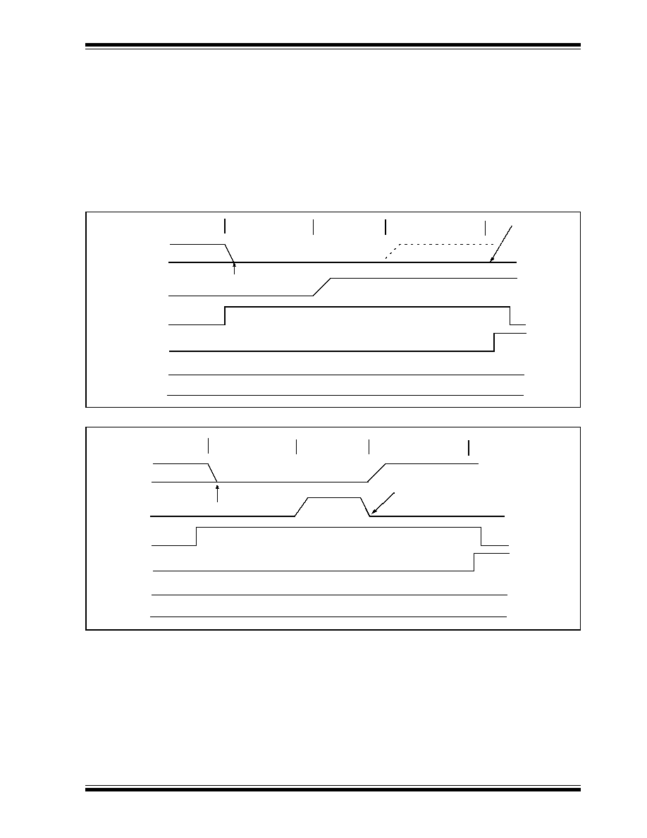
PIC18CXX2
©
7/99 Microchip Technology Inc.
Preliminary
DS39026B-page 149
14.3.16.3 BUS COLLISION DURING A STOP
CONDITION
Bus collision occurs during a STOP condition if:
a)
After the SDA pin has been de-asserted and
allowed to float high, SDA is sampled low after
the BRG has timed out.
b)
After the SCL pin is de-asserted, SCL is sam-
pled low before SDA goes high.
The STOP condition begins with SDA asserted low.
When SDA is sampled low, the SCL pin is allowed to
float. When the pin is sampled high (clock arbitration),
the baud rate generator is loaded with SSPADD<6:0>
and counts down to 0. After the BRG times out SDA is
sampled. If SDA is sampled low, a bus collision has
occurred. This is due to another master attempting to
drive a data '0' (Figure 14-29). If the SCL pin is sampled
low before SDA is allowed to float high, a bus collision
occurs. This is another case of another master attempt-
ing to drive a data '0' (Figure 14-30).
FIGURE 14-29: BUS COLLISION DURING A STOP CONDITION (CASE 1)
FIGURE 14-30: BUS COLLISION DURING A STOP CONDITION (CASE 2)
SDA
SCL
BCLIF
PEN
P
SSPIF
T
BRG
T
BRG
T
BRG
SDA asserted low
SDA sampled
low after T
BRG
,
Set BCLIF
'0'
'0'
SDA
SCL
BCLIF
PEN
P
SSPIF
T
BRG
T
BRG
T
BRG
Assert SDA
SCL goes low before SDA goes high
Set BCLIF
'0'
'0'

PIC18CXX2
DS39026B-page 150
Preliminary
©
7/99 Microchip Technology Inc.
NOTES:

PIC18CXX2
©
7/99 Microchip Technology Inc.
Preliminary
DS39026B-page 151
15.0
ADDRESSABLE UNIVERSAL
SYNCHRONOUS
ASYNCHRONOUS RECEIVER
TRANSMITTER (USART)
The Universal Synchronous Asynchronous Receiver
Transmitter (USART) module is one of the two serial
I/O modules. (USART is also known as a Serial Com-
munications Interface or SCI). The USART can be con-
figured as a full duplex asynchronous system that can
communicate with peripheral devices, such as CRT ter-
minals and personal computers, or it can be configured
as a half duplex synchronous system that can commu-
nicate with peripheral devices, such as A/D or D/A inte-
grated circuits, Serial EEPROMs, etc.
The USART can be configured in the following modes:
∑ Asynchronous (full duplex)
∑ Synchronous - Master (half duplex)
∑ Synchronous - Slave (half duplex)
Bit SPEN (RCSTA<7>) and bits TRISC<7:6> have to
be set in order to configure pins RC6/TX/CK and
RC7/RX/DT as the Universal Synchronous Asynchro-
nous Receiver Transmitter.
Register 15-1: TXSTA: Transmit Status and Control Register
R/W-0
R/W-0
R/W-0
R/W-0
U-0
R/W-0
R-1
R/W-0
CSRC
TX9
TXEN
SYNC
--
BRGH
TRMT
TX9D
bit 7
bit 0
bit 7
CSRC: Clock Source Select bit
Asynchronous mode
Don't care
Synchronous mode
1
= Master mode (Clock generated internally from BRG)
0
= Slave mode (Clock from external source)
bit 6
TX9: 9-bit Transmit Enable bit
1
= Selects 9-bit transmission
0
= Selects 8-bit transmission
bit 5
TXEN: Transmit Enable bit
1
= Transmit enabled
0
= Transmit disabled
Note:
SREN/CREN overrides TXEN in SYNC mode.
bit 4
SYNC: USART Mode Select bit
1
= Synchronous mode
0
= Asynchronous mode
bit 3
Unimplemented: Read as '0'
bit 2
BRGH: High Baud Rate Select bit
Asynchronous mode
1
= High speed
0
= Low speed
Synchronous mode
Unused in this mode
bit 1
TRMT: Transmit Shift Register Status bit
1
= TSR empty
0
= TSR full
bit 0
TX9D: 9th bit of transmit data. Can be Address/Data bit or a parity bit.
Legend:
R = Readable bit
W = Writable bit
U = Unimplemented bit, read as `0'
- n = Value at POR reset
'1' = Bit is set
'0' = Bit is cleared
x = Bit is unknown

PIC18CXX2
DS39026B-page 152
Preliminary
©
7/99 Microchip Technology Inc.
Register 15-2: RCSTA: Receive Status and Control Register
R/W-0
R/W-0
R/W-0
R/W-0
R/W-0
R-0
R-0
R-x
SPEN
RX9
SREN
CREN
ADDEN
FERR
OERR
RX9D
bit 7
bit 0
bit 7
SPEN: Serial Port Enable bit
1
= Serial port enabled (Configures RX/DT and TX/CK pins as serial port pins)
0
= Serial port disabled
bit 6
RX9: 9-bit Receive Enable bit
1
= Selects 9-bit reception
0
= Selects 8-bit reception
bit 5
SREN: Single Receive Enable bit
Asynchronous mode
Don't care
Synchronous mode - master
1
= Enables single receive
0
= Disables single receive
This bit is cleared after reception is complete.
Synchronous mode - slave
Unused in this mode
bit 4
CREN: Continuous Receive Enable bit
Asynchronous mode
1
= Enables continuous receive
0
= Disables continuous receive
Synchronous mode
1
= Enables continuous receive until enable bit CREN is cleared (CREN overrides SREN)
0
= Disables continuous receive
bit 3
ADDEN: Address Detect Enable bit
Asynchronous mode 9-bit (RX9 = 1)
1
= Enables address detection, enable interrupt and load of the receive buffer
when RSR<8> is set
0
= Disables address detection, all bytes are received, and ninth bit can be used as parity bit
bit 2
FERR: Framing Error bit
1
= Framing error (Can be updated by reading RCREG register and receive next valid byte)
0
= No framing error
bit 1
OERR: Overrun Error bit
1
= Overrun error (Can be cleared by clearing bit CREN)
0
= No overrun error
bit 0
RX9D: 9th bit of received data, can be Address/Data bit or a parity bit.
Legend:
R = Readable bit
W = Writable bit
U = Unimplemented bit, read as `0'
- n = Value at POR reset
'1' = Bit is set
'0' = Bit is cleared
x = Bit is unknown
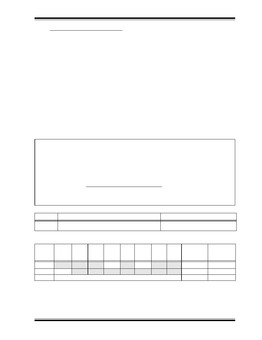
PIC18CXX2
©
7/99 Microchip Technology Inc.
Preliminary
DS39026B-page 153
15.1
USART Baud Rate Generator (BRG)
The BRG supports both the Asynchronous and Syn-
chronous modes of the USART. It is a dedicated 8-bit
baud rate generator. The SPBRG register controls the
period of a free running 8-bit timer. In asynchronous
mode, bit BRGH (TXSTA<2>) also controls the baud
rate. In synchronous mode, bit BRGH is ignored.
Table 15-1 shows the formula for computation of the
baud rate for different USART modes, which only apply
in master mode (internal clock).
Given the desired baud rate and Fosc, the nearest inte-
ger value for the SPBRG register can be calculated
using the formula in Table 15-1. From this, the error in
baud rate can be determined.
Example 15-1 shows the calculation of the baud rate
error for the following conditions:
F
OSC
= 16 MHz
Desired Baud Rate = 9600
BRGH = 0
SYNC = 0
It may be advantageous to use the high baud rate
(BRGH = 1) even for slower baud clocks. This is
because the F
OSC
/(16(X + 1)) equation can reduce the
baud rate error in some cases.
Writing a new value to the SPBRG register causes the
BRG timer to be reset (or cleared). This ensures the
BRG does not wait for a timer overflow before output-
ting the new baud rate.
15.1.1
SAMPLING
The data on the RC7/RX/DT pin is sampled three times
by a majority detect circuit to determine if a high or a
low level is present at the RX pin.
EXAMPLE 15-1: CALCULATING BAUD RATE ERROR
TABLE 15-1:
BAUD RATE FORMULA
TABLE 15-2:
REGISTERS ASSOCIATED WITH BAUD RATE GENERATOR
SYNC
BRGH = 0 (Low Speed)
BRGH = 1 (High Speed)
0
1
(Asynchronous) Baud Rate = F
OSC
/(64(X+1))
(Synchronous) Baud Rate = F
OSC
/(4(X+1))
Baud Rate= F
OSC
/(16(X+1))
NA
X = value in SPBRG (0 to 255)
Name
Bit 7
Bit 6
Bit 5
Bit 4
Bit 3
Bit 2
Bit 1
Bit 0
Value on
POR,
BOR
Value on all
other resets
TXSTA
CSRC
TX9
TXEN
SYNC
--
BRGH
TRMT
TX9D
0000 -010
0000 -010
RCSTA
SPEN
RX9
SREN
CREN
--
FERR
OERR
RX9D
0000 -00x
0000 -00x
SPBRG
Baud Rate Generator Register
0000 0000
0000 0000
Legend: x
= unknown,
- = unimplemented read as '0'.
Shaded cells are not used by the BRG.
Desired Baud rate
= Fosc / (64 (X + 1))
Solving for X:
X
= ( (Fosc / Desired Baud rate) / 64 ) - 1
X
= ((16000000 / 9600) / 64) - 1
X
= [25.042] = 25
Calculated Baud Rate
= 16000000 / (64 (25 + 1))
= 9615
Error
= (Calculated Baud Rate - Desired Baud Rate)
Desired Baud Rate
= (9615 - 9600) / 9600
= 0.16%

PIC18CXX2
DS39026B-page 154
Preliminary
©
7/99 Microchip Technology Inc.
TABLE 15-3:
BAUD RATES FOR SYNCHRONOUS MODE
BAUD
RATE
(K)
F
OSC
= 20 MHz
SPBRG
value
(decimal)
16 MHz
SPBRG
value
(decimal)
10 MHz
SPBRG
value
(decimal)
7.15909 MHz
SPBRG
value
(decimal)
%
%
%
%
0.3
NA
-
-
NA
-
-
NA
-
-
NA
-
-
1.2
NA
-
-
NA
-
-
NA
-
-
NA
-
-
2.4
NA
-
-
NA
-
-
NA
-
-
NA
-
-
9.6
NA
-
-
NA
-
-
9.766
+1.73
255
9.622
+0.23
185
19.2
19.53
+1.73
255
19.23
+0.16
207
19.23
+0.16
129
19.24
+0.23
92
76.8
76.92
+0.16
64
76.92
+0.16
51
75.76
-1.36
32
77.82
+1.32
22
96
96.15
+0.16
51
95.24
-0.79
41
96.15
+0.16
25
94.20
-1.88
18
300
294.1
-1.96
16
307.69
+2.56
12
312.5
+4.17
7
298.3
-0.57
5
500
500
0
9
500
0
7
500
0
4
NA
-
-
HIGH
5000
-
0
4000
-
0
2500
-
0
1789.8
-
0
LOW
19.53
-
255
15.625
-
255
9.766
-
255
6.991
-
255
BAUD
RATE
(K)
F
OSC
= 5.0688 MHz
4 MHz
SPBRG
value
(decimal)
3.579545 MHz
SPBRG
value
(decimal)
1 MHz
SPBRG
value
(decimal)
32.768 kHz
SPBRG
value
(decimal)
%
SPBRG
%
%
%
%
0.3
NA
-
-
NA
-
-
NA
-
-
NA
-
-
0.303
+1.14
26
1.2
NA
-
-
NA
-
-
NA
-
-
1.202
+0.16
207
1.170
-2.48
6
2.4
NA
-
-
NA
-
-
NA
-
-
2.404
+0.16
103
NA
-
-
9.6 9.6 0
131
9.615
+0.16
103
9.622
+0.23
92
9.615
+0.16
25
NA
-
-
19.2
19.2 0
65
19.231
+0.16
51
19.04
-0.83
46
19.24
+0.16
12
NA
-
-
76.8
79.2 +3.13
15
76.923
+0.16
12
74.57
-2.90
11
83.34
+8.51
2
NA
-
-
96
97.48
+1.54
12
1000
+4.17
9
99.43
+3.57
8
NA
-
-
NA
-
-
300
316.8
+5.60
3
NA
-
-
298.3
-0.57
2
NA
-
-
NA
-
-
500
NA
-
-
NA
-
-
NA
-
-
NA
-
-
NA
-
-
HIGH
1267
-
0
100
-
0
894.9
-
0
250
-
0
8.192
-
0
LOW
4.950
-
255
3.906
-
255
3.496
-
255
0.9766
-
255
0.032
-
255

PIC18CXX2
©
7/99 Microchip Technology Inc.
Preliminary
DS39026B-page 155
TABLE 15-4:
BAUD RATES FOR ASYNCHRONOUS MODE (BRGH = 0)
BAUD
RATE
(K)
F
OSC
= 20 MHz
SPBRG
value
(decimal)
16 MHz
SPBRG
value
(decimal)
10 MHz
SPBRG
value
(decimal)
7.15909 MHz
SPBRG
value
(decimal)
%
%
%
%
0.3
NA
-
-
NA -
-
NA -
-
NA
-
-
1.2
1.221
+1.73
255
1.202
+0.16
207
1.202
+0.16
129
1.203
+0.23
92
2.4
2.404
+0.16
129
2.404
+0.16
103
2.404
+0.16
64
2.380
-0.83
46
9.6 9.469
-1.36
32
9.615
+0.16
25
9.766
+1.73
15
9.322
-2.90
11
19.2
19.53
+1.73
15
19.23
+0.16
12
19.53
+1.73
7
18.64
-2.90
5
76.8
78.13
+1.73
3
83.33
+8.51
2
78.13
+1.73
1
NA
-
-
96
104.2
+8.51
2
NA
-
-
NA
-
-
NA
-
-
300
312.5
+4.17
0
NA
-
-
NA
-
-
NA
-
-
500
NA
-
-
NA
-
-
NA
-
-
NA
-
-
HIGH
312.5
-
0
250
-
0
156.3
-
0
111.9
-
0
LOW 1.221
-
255
0.977
-
255
0.6104
-
255
0.437
-
255
BAUD
RATE
(K)
F
OSC
= 5.0688 MHz
4 MHz
SPBRG
value
(decimal)
3.579545 MHz
SPBRG
value
(decimal)
1 MHz
SPBRG
value
(decimal)
32.768 kHz
SPBRG
value
(decimal)
%
SPBRG
%
%
%
%
0.3
0.31
+3.13
255
0.3005
-0.17
207
0.301
+0.23
185
0.300
+0.16
51
0.256
-14.67
1
1.2 1.2
0
65
1.202
+1.67
51
1.190
-0.83
46
1.202
+0.16
12
NA
-
-
2.4
2.4
0 32
2.404
+1.67
25
2.432
+1.32
22
2.232
-6.99
6
NA
-
-
9.6 9.9
+3.13
7
NA
-
-
9.322
-2.90
5
NA
-
-
NA
-
-
19.2
19.8
+3.13
3
NA
-
-
18.64
-2.90
2
NA
-
-
NA
-
-
76.8
79.2
+3.13
0
NA
-
-
NA
-
-
NA
-
-
NA
-
-
96
NA
-
-
NA
-
-
NA
-
-
NA
-
-
NA
-
-
300
NA
-
-
NA
-
-
NA
-
-
NA
-
-
NA
-
-
500
NA
-
-
NA
-
-
NA
-
-
NA
-
-
NA
-
-
HIGH
79.2
-
0
62.500
-
0
55.93
-
0
15.63
-
0
0.512
-
0
LOW
0.3094
-
255
3.906
-
255
0.2185
-
255
0.0610
-
255
0.0020
-
255

PIC18CXX2
DS39026B-page 156
Preliminary
©
7/99 Microchip Technology Inc.
TABLE 15-5:
BAUD RATES FOR ASYNCHRONOUS MODE (BRGH = 1)
BAUD
RATE
(K)
F
OSC
= 20 MHz
SPBRG
value
(decimal)
16 MHz
SPBRG
value
(decimal)
10 MHz
SPBRG
value
(decimal)
7.16 MHz
SPBRG
value
(decimal)
%
%
%
%
9.6
9.615
+0.16
129
9.615
+0.16
103
9.615
+0.16
64
9.520
-0.83
46
19.2
19.230
+0.16
64
19.230
+0.16
51
18.939
-1.36
32
19.454
+1.32
22
38.4
37.878
-1.36
32
38.461
+0.16
25
39.062
+1.7
15
37.286
-2.90
11
57.6
56.818
-1.36
21
58.823
+2.12
16
56.818
-1.36
10
55.930
-2.90
7
115.2
113.636
-1.36
10
111.111
-3.55
8
125
+8.51
4
111.860
-2.90
3
250
250
0
4
250
0
3
NA
-
-
NA
-
-
625
625
0
1
NA
-
-
625
0
0
NA
-
-
1250
1250
0
0
NA
-
-
NA
-
-
NA
-
-
BAUD
RATE
(K)
F
OSC
= 5.068
SPBRG
value
(decimal)
4 MHz
SPBRG
value
(decimal)
3.579 MHz
SPBRG
value
(decimal)
1 MHz
SPBRG
value
(decimal)
32.768 kHz
SPBRG
value
(decimal)
%
%
%
%
%
9.6
9.6
0
32
NA
-
-
9.727
+1.32
22
8.928
-6.99
6
NA
-
-
19.2
18.645
-2.94
16
1.202
+0.17
207
18.643
-2.90
11
20.833
+8.51
2
NA
-
-
38.4
39.6
+3.12 7
2.403
+0.13
103
37.286
-2.90
5
31.25
-18.61
1
NA -
-
57.6
52.8
-8.33
5
9.615
+0.16
25
55.930
-2.90
3
62.5
+8.51
0
NA
-
-
115.2
105.6
-8.33
2
19.231
+0.16
12
111.86
-2.90
1
NA
-
-
NA
-
-
250
NA
-
-
NA
-
-
223.72
-10.51
0
NA
-
-
NA
-
-
625
NA
-
-
NA
-
-
NA
-
-
NA
-
-
NA
-
-
1250
NA
-
-
NA
-
-
NA
-
-
NA
-
-
NA
-
-
PIC18CXX2
©
7/99 Microchip Technology Inc.
Preliminary
DS39026B-page 157
15.2
USART Asynchronous Mode
In this mode, the USART uses standard non-return-to-
zero (NRZ) format (one start bit, eight or nine data bits
and one stop bit). The most common data format is
8-bits. An on-chip dedicated 8-bit baud rate generator
can be used to derive standard baud rate frequencies
from the oscillator. The USART transmits and receives
the LSb first. The USART's transmitter and receiver are
functionally independent, but use the same data format
and baud rate. The baud rate generator produces a
clock, either x16 or x64 of the bit shift rate, depending
on bit BRGH (TXSTA<2>). Parity is not supported by
the hardware, but can be implemented in software (and
stored as the ninth data bit). Asynchronous mode is
stopped during SLEEP.
Asynchronous mode is selected by clearing bit SYNC
(TXSTA<4>).
The USART Asynchronous module consists of the fol-
lowing important elements:
∑ Baud Rate Generator
∑ Sampling Circuit
∑ Asynchronous Transmitter
∑ Asynchronous Receiver
15.2.1
USART ASYNCHRONOUS TRANSMITTER
The USART transmitter block diagram is shown in
Figure 15-1. The heart of the transmitter is the transmit
(serial) shift register (TSR). The shift register obtains its
data from the read/write transmit buffer, TXREG. The
TXREG register is loaded with data in software. The
TSR register is not loaded until the STOP bit has been
transmitted from the previous load. As soon as the
STOP bit is transmitted, the TSR is loaded with new
data from the TXREG register (if available). Once the
TXREG register transfers the data to the TSR register
(occurs in one T
CY
), the TXREG register is empty and
flag bit TXIF (PIR1<4>) is set. This interrupt can be
enabled/disabled by setting/clearing enable bit TXIE
( PIE1<4>). Flag bit TXIF will be set regardless of the
state of enable bit TXIE and cannot be cleared in soft-
ware. It will reset only when new data is loaded into the
TXREG register. While flag bit TXIF indicated the sta-
tus of the TXREG register, another bit TRMT
(TXSTA<1>) shows the status of the TSR register. Sta-
tus bit TRMT is a read only bit, which is set when the
TSR register is empty. No interrupt logic is tied to this
bit, so the user has to poll this bit in order to determine
if the TSR register is empty.
Steps to follow when setting up an asynchronous trans-
mission:
1.
Initialize the SPBRG register for the appropriate
baud rate. If a high speed baud rate is desired,
set bit BRGH. (Section 15.1)
2.
Enable the asynchronous serial port by clearing
bit SYNC and setting bit SPEN.
3.
If interrupts are desired, set enable bit TXIE.
4.
If 9-bit transmission is desired, set transmit bit
TX9. Can be used as address/data bit.
5.
Enable the transmission by setting bit TXEN,
which will also set bit TXIF.
6.
If 9-bit transmission is selected, the ninth bit
should be loaded in bit TX9D.
7.
Load data to the TXREG register (starts trans-
mission).
FIGURE 15-1: USART TRANSMIT BLOCK DIAGRAM
Note 1: The TSR register is not mapped in data
memory, so it is not available to the user.
Note 2: Flag bit TXIF is set when enable bit TXEN
is set.
TXIF
TXIE
Interrupt
TXEN
Baud Rate CLK
SPBRG
Baud Rate Generator
TX9D
MSb
LSb
Data Bus
TXREG register
TSR register
(8)
0
TX9
TRMT
SPEN
RC6/TX/CK pin
Pin Buffer
and Control
8
∑ ∑ ∑
PIC18CXX2
DS39026B-page 158
Preliminary
©
7/99 Microchip Technology Inc.
FIGURE 15-2: ASYNCHRONOUS TRANSMISSION
FIGURE 15-3: ASYNCHRONOUS TRANSMISSION (BACK TO BACK)
TABLE 15-6:
REGISTERS ASSOCIATED WITH ASYNCHRONOUS TRANSMISSION
Name
Bit 7
Bit 6
Bit 5
Bit 4
Bit 3
Bit 2
Bit 1
Bit 0
Value on
POR,
BOR
Value on
all other
Resets
INTCON
GIE/GIEH
PEIE/
GIEL
TMR0IE INT0IE
RBIE
TMR0IF
INT0IF
RBIF
0000 000x
0000 000u
PIR1
PSPIF
(1)
ADIF
RCIF
TXIF
SSPIF CCP1IF TMR2IF
TMR1IF
0000 0000
0000 0000
PIE1
PSPIE
(1)
ADIE
RCIE
TXIE
SSPIE CCP1IE TMR2IE
TMR1IE
0000 0000
0000 0000
IPR1
PSPIP
(1)
ADIP
RCIP
TXIP
SSPIP CCP1IP TMR2IP
TMR1IP
0000 0000
0000 0000
RCSTA
SPEN
RX9
SREN
CREN
--
FERR
OERR
RX9D
0000 -00x
0000 -00x
TXREG
USART Transmit Register
0000 0000
0000 0000
TXSTA
CSRC
TX9
TXEN
SYNC
--
BRGH
TRMT
TX9D
0000 -010
0000 -010
SPBRG
Baud Rate Generator Register
0000 0000
0000 0000
Legend: x = unknown, - = unimplemented locations read as '0'.
Shaded cells are not used for Asynchronous Transmission.
Note 1: The PSPIF, PSPIE and PSPIP bits are reserved on the PIC18C2X2 devices. Always maintain these bits
clear.
WORD 1
Stop Bit
WORD 1
Transmit Shift Reg
Start Bit
Bit 0
Bit 1
Bit 7/8
Write to TXREG
Word 1
BRG output
(shift clock)
RC6/TX/CK (pin)
TXIF bit
(Transmit buffer
reg. empty flag)
TRMT bit
(Transmit shift
reg. empty flag)
Transmit Shift Reg.
Write to TXREG
BRG output
(shift clock)
RC6/TX/CK (pin)
TXIF bit
(interrupt reg. flag)
TRMT bit
(Transmit shift
reg. empty flag)
Word 1
Word 2
WORD 1
WORD 2
Start Bit
Stop Bit
Start Bit
Transmit Shift Reg.
WORD 1
WORD 2
Bit 0
Bit 1
Bit 7/8
Bit 0
Note: This timing diagram shows two consecutive transmissions.
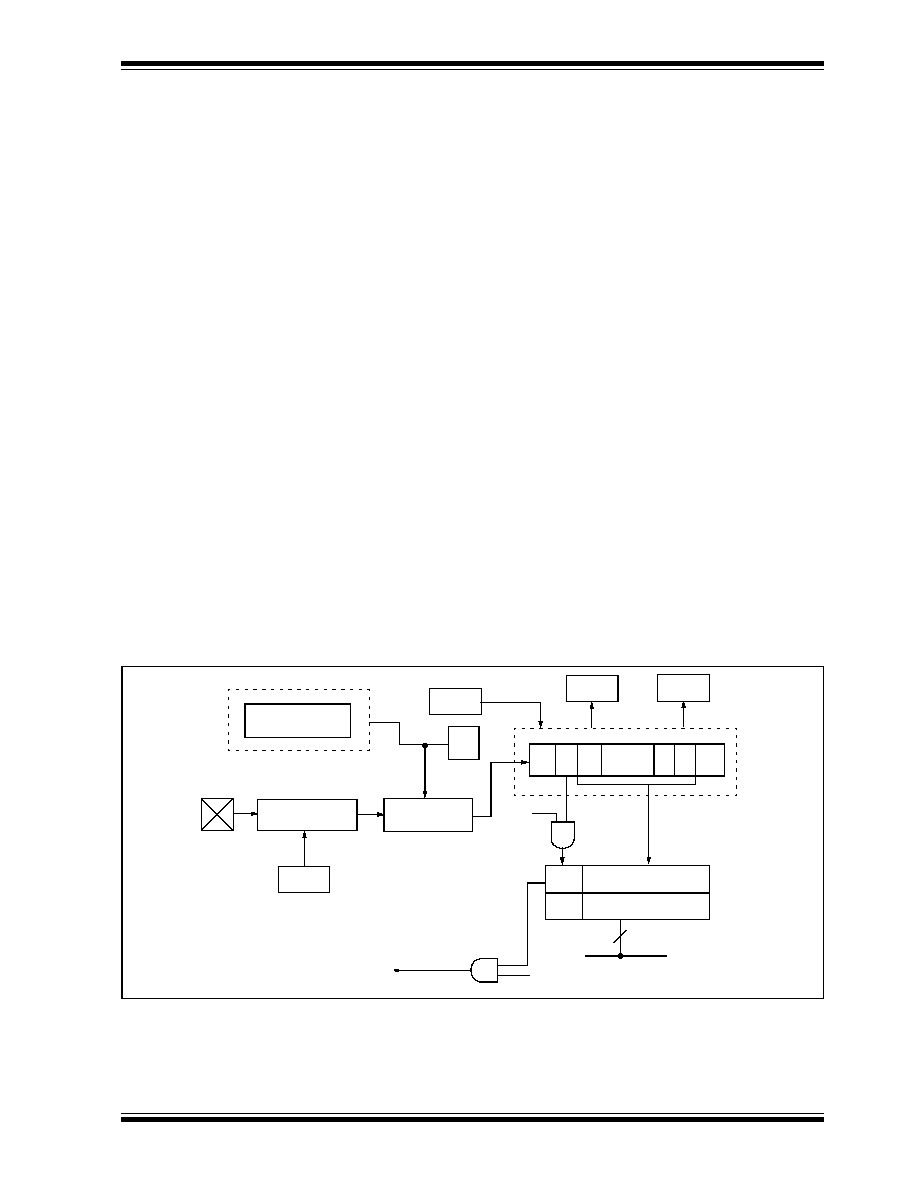
PIC18CXX2
©
7/99 Microchip Technology Inc.
Preliminary
DS39026B-page 159
15.2.2
USART ASYNCHRONOUS RECEIVER
The receiver block diagram is shown in Figure 15-4.
The data is received on the RC7/RX/DT pin and drives
the data recovery block. The data recovery block is
actually a high speed shifter operating at x16 times the
baud rate, whereas the main receive serial shifter oper-
ates at the bit rate or at F
OSC
. This mode would typi-
cally be used in RS-232 systems.
Steps to follow when setting up an Asynchronous
Reception:
1.
Initialize the SPBRG register for the appropriate
baud rate. If a high speed baud rate is desired,
set bit BRGH. (Section 15.1).
2.
Enable the asynchronous serial port by clearing
bit SYNC and setting bit SPEN.
3.
If interrupts are desired, set enable bit RCIE.
4.
If 9-bit reception is desired, set bit RX9.
5.
Enable the reception by setting bit CREN.
6.
Flag bit RCIF will be set when reception is com-
plete and an interrupt will be generated if enable
bit RCIE was set.
7.
Read the RCSTA register to get the ninth bit (if
enabled) and determine if any error occurred
during reception.
8.
Read the 8-bit received data by reading the
RCREG register.
9.
If any error occurred, clear the error by clearing
enable bit CREN.
15.2.3
SETTING UP 9-BIT MODE WITH ADDRESS
DETECT
This mode would typically be used in RS-485 systems.
Steps to follow when setting up an Asynchronous
Reception with Address Detect Enable:
1.
Initialize the SPBRG register for the appropriate
baud rate. If a high speed baud rate is required,
set the BRGH bit.
2.
Enable the asynchronous serial port by clearing
the SYNC bit and setting the SPEN bit.
3.
If interrupts are required, set the RCEN bit and
select the desired priority level with the RCIP bit.
4.
Set the RX9 bit to enable 9-bit reception.
5.
Set the ADDEN bit to enable address detect.
6.
Enable reception by setting the CREN bit.
7.
The RCIF bit will be set when reception is com-
plete. The interrupt will be acknowledged if the
RCIE and GIE bits are set.
8.
Read the RCSTA register to determine if any
error occurred during reception, as well as read
bit 9 of data (if applicable).
9.
Read RCREG to determine if the device is being
addressed.
10. If any error occurred, clear the CREN bit.
11. If the device has been addressed, clear the
ADDEN bit to allow all received data into the
receive buffer and interrupt the CPU.
FIGURE 15-4: USART RECEIVE BLOCK DIAGRAM
x64 Baud Rate CLK
SPBRG
Baud Rate Generator
RC7/RX/DT
Pin Buffer
and Control
SPEN
Data
Recovery
CREN
OERR
FERR
RSR Register
MSb
LSb
RX9D
RCREG Register
FIFO
Interrupt
RCIF
RCIE
Data Bus
8
˜
64
˜
16
or
Stop
Start
(8)
7
1
0
RX9
∑ ∑ ∑
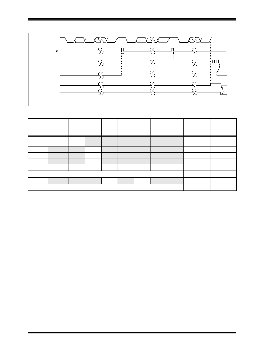
PIC18CXX2
DS39026B-page 160
Preliminary
©
7/99 Microchip Technology Inc.
FIGURE 15-5: ASYNCHRONOUS RECEPTION
TABLE 15-7:
REGISTERS ASSOCIATED WITH ASYNCHRONOUS RECEPTION
Name
Bit 7
Bit 6
Bit 5
Bit 4
Bit 3
Bit 2
Bit 1
Bit 0
Value on
POR,
BOR
Value on
all other
Resets
INTCON
GIE/GIEH
PEIE/
GIEL
TMR0IE INT0IE
RBIE
TMR0IF INT0IF
RBIF
0000 000x
0000 000u
PIR1
PSPIF
(1)
ADIF
RCIF
TXIF
SSPIF CCP1IF TMR2IF TMR1IF
0000 0000
0000 0000
PIE1
PSPIE
(1)
ADIE
RCIE
TXIE
SSPIE CCP1IE TMR2IE TMR1IE
0000 0000
0000 0000
IPR1
PSPIP
(1)
ADIP
RCIP
TXIP
SSPIP CCP1IP TMR2IP TMR1IP
0000 0000
0000 0000
RCSTA
SPEN
RX9
SREN
CREN
--
FERR
OERR
RX9D
0000 -00x
0000 -00x
RCREG
USART Receive Register
0000 0000
0000 0000
TXSTA
CSRC
TX9
TXEN
SYNC
--
BRGH
TRMT
TX9D
0000 -010
0000 -010
SPBRG
Baud Rate Generator Register
0000 0000
0000 0000
Legend: x = unknown, - = unimplemented locations read as '0'.
Shaded cells are not used for Asynchronous Reception.
Note 1: The PSPIF, PSPIE and PSPIP bits are reserved on the PIC18C2X2 devices. Always maintain these bits
clear.
Start
bit
bit7/8
bit1
bit0
bit7/8
bit0
Stop
bit
Start
bit
Start
bit
bit7/8
Stop
bit
RX (pin)
reg
Rcv buffer reg
Rcv shift
Read Rcv
buffer reg
RCREG
RCIF
(interrupt flag)
OERR bit
CREN
WORD 1
RCREG
WORD 2
RCREG
Stop
bit
Note: This timing diagram shows three words appearing on the RX input. The RCREG (receive buffer) is read after the third word,
causing the OERR (overrun) bit to be set.
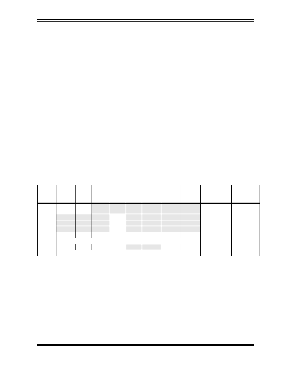
PIC18CXX2
©
7/99 Microchip Technology Inc.
Preliminary
DS39026B-page 161
15.3
USART Synchronous Master Mode
In Synchronous Master mode, the data is transmitted in
a half-duplex manner, (i.e. transmission and reception
do not occur at the same time). When transmitting data,
the reception is inhibited and vice versa. Synchronous
mode is entered by setting bit SYNC (TXSTA<4>). In
addition, enable bit SPEN (RCSTA<7>) is set in order
to configure the RC6/TX/CK and RC7/RX/DT I/O pins
to CK (clock) and DT (data) lines respectively. The
Master mode indicates that the processor transmits the
master clock on the CK line. The Master mode is
entered by setting bit CSRC (TXSTA<7>).
15.3.1
USART SYNCHRONOUS MASTER
TRANSMISSION
The USART transmitter block diagram is shown in
Figure 15-1. The heart of the transmitter is the transmit
(serial) shift register (TSR). The shift register obtains its
data from the read/write transmit buffer register
TXREG. The TXREG register is loaded with data in
software. The TSR register is not loaded until the last
bit has been transmitted from the previous load. As
soon as the last bit is transmitted, the TSR is loaded
with new data from the TXREG (if available). Once the
TXREG register transfers the data to the TSR register
(occurs in one Tcycle), the TXREG is empty and inter-
rupt bit TXIF (PIR1<4>) is set. The interrupt can be
enabled/disabled by setting/clearing enable bit TXIE
(PIE1<4>). Flag bit TXIF will be set, regardless of the
state of enable bit TXIE, and cannot be cleared in soft-
ware. It will reset only when new data is loaded into the
TXREG register. While flag bit TXIF indicates the status
of the TXREG register, another bit TRMT (TXSTA<1>)
shows the status of the TSR register. TRMT is a read
only bit, which is set when the TSR is empty. No inter-
rupt logic is tied to this bit, so the user has to poll this
bit in order to determine if the TSR register is empty.
The TSR is not mapped in data memory, so it is not
available to the user.
Steps to follow when setting up a Synchronous Master
Transmission:
1.
Initialize the SPBRG register for the appropriate
baud rate (Section 15.1).
2.
Enable the synchronous master serial port by
setting bits SYNC, SPEN, and CSRC.
3.
If interrupts are desired, set enable bit TXIE.
4.
If 9-bit transmission is desired, set bit TX9.
5.
Enable the transmission by setting bit TXEN.
6.
If 9-bit transmission is selected, the ninth bit
should be loaded in bit TX9D.
7.
Start transmission by loading data to the
TXREG register.
TABLE 15-8:
REGISTERS ASSOCIATED WITH SYNCHRONOUS MASTER TRANSMISSION
Name
Bit 7
Bit 6
Bit 5
Bit 4
Bit 3
Bit 2
Bit 1
Bit 0
Value on
POR,
BOR
Value on all
other Resets
INTCON
GIE/
GIEH
PEIE/
GIEL
TMR0IE INT0IE
RBIE
TMR0IF
INT0IF
RBIF
0000 000x
0000 000u
PIR1
PSPIF
(1)
ADIF
RCIF
TXIF
SSPIF
CCP1IF
TMR2IF
TMR1IF
0000 0000
0000 0000
PIE1
PSPIE
(1)
ADIE
RCIE
TXIE
SSPIE
CCP1IE
TMR2IE
TMR1IE
0000 0000
0000 0000
IPR1
PSPIP
(1)
ADIP
RCIP
TXIP
SSPIP
CCP1IP
TMR2IP
TMR1IP
0000 0000
0000 0000
RCSTA
SPEN
RX9
SREN
CREN
--
FERR
OERR
RX9D
0000 -00x
0000 -00x
TXREG
USART Transmit Register
0000 0000
0000 0000
TXSTA
CSRC
TX9
TXEN
SYNC
--
BRGH
TRMT
TX9D
0000 -010
0000 -010
SPBRG
Baud Rate Generator Register
0000 0000
0000 0000
Legend: x = unknown, -- = unimplemented, read as '0'.
Shaded cells are not used for Synchronous Master Transmission.
Note 1: The PSPIF, PSPIE and PSPIP bits are reserved on the PIC18C2X2 devices. Always maintain these bits clear.
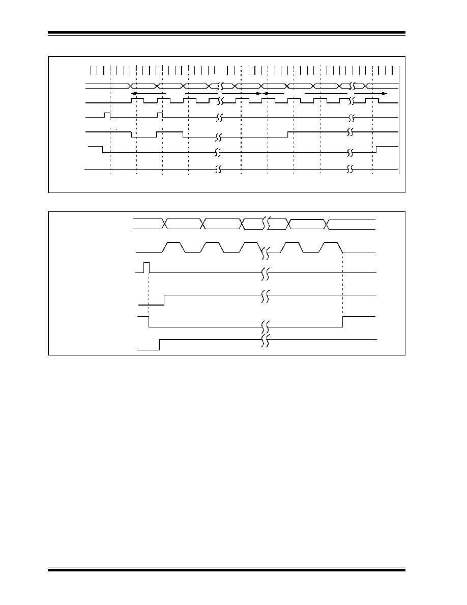
PIC18CXX2
DS39026B-page 162
Preliminary
©
7/99 Microchip Technology Inc.
FIGURE 15-6: SYNCHRONOUS TRANSMISSION
FIGURE 15-7: SYNCHRONOUS TRANSMISSION (THROUGH TXEN)
Bit 0
Bit 1
Bit 7
WORD 1
Q1 Q2 Q3 Q4 Q1 Q2 Q3 Q4 Q1 Q2 Q3 Q4 Q1 Q2 Q3 Q4 Q1 Q2 Q3 Q4
Q3 Q4 Q1 Q2 Q3 Q4 Q1 Q2 Q3 Q4 Q1 Q2 Q3 Q4 Q1 Q2 Q3 Q4 Q1 Q2 Q3 Q4 Q1 Q2 Q3 Q4
Bit 2
Bit 0
Bit 1
Bit 7
RC7/RX/DT pin
RC6/TX/CK pin
Write to
TXREG reg
TXIF bit
(Interrupt flag)
TRMT
TXEN bit
'1'
'1'
Note: Sync master mode; SPBRG = '0'. Continuous transmission of two 8-bit words
WORD 2
TRMT bit
Write word1
Write word2
RC7/RX/DT pin
RC6/TX/CK pin
Write to
TXREG reg
TXIF bit
TRMT bit
bit0
bit1
bit2
bit6
bit7
TXEN bit
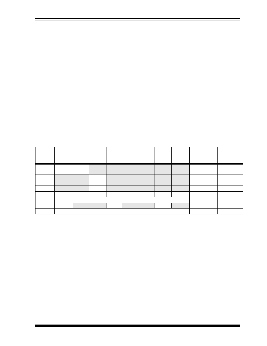
PIC18CXX2
©
7/99 Microchip Technology Inc.
Preliminary
DS39026B-page 163
15.3.2
USART SYNCHRONOUS MASTER
RECEPTION
Once synchronous mode is selected, reception is
enabled by setting either enable bit SREN (RCSTA<5>)
or enable bit CREN (RCSTA<4>). Data is sampled on
the RC7/RX/DT pin on the falling edge of the clock. If
enable bit SREN is set, only a single word is received.
If enable bit CREN is set, the reception is continuous
until CREN is cleared. If both bits are set, then CREN
takes precedence.
Steps to follow when setting up a Synchronous Master
Reception:
1.
Initialize the SPBRG register for the appropriate
baud rate. (Section 15.1)
2.
Enable the synchronous master serial port by
setting bits SYNC, SPEN and CSRC.
3.
Ensure bits CREN and SREN are clear.
4.
If interrupts are desired, set enable bit RCIE.
5.
If 9-bit reception is desired, set bit RX9.
6.
If a single reception is required, set bit SREN.
For continuous reception, set bit CREN.
7.
Interrupt flag bit RCIF will be set when reception
is complete and an interrupt will be generated if
the enable bit RCIE was set.
8.
Read the RCSTA register to get the ninth bit (if
enabled) and determine if any error occurred
during reception.
9.
Read the 8-bit received data by reading the
RCREG register.
10. If any error occurred, clear the error by clearing
bit CREN.
TABLE 15-9:
REGISTERS ASSOCIATED WITH SYNCHRONOUS MASTER RECEPTION
Name
Bit 7
Bit 6
Bit 5
Bit 4
Bit 3
Bit 2
Bit 1
Bit 0
Value on
POR,
BOR
Value on all
other
Resets
INTCON
GIE/
GIEH
PEIE/
GIEL
TMR0IE INT0IE
RBIE
TMR0IF
INT0IF
RBIF
0000 000x
0000 000u
PIR1
PSPIF
(1)
ADIF
RCIF
TXIF
SSPIF CCP1IF TMR2IF TMR1IF
0000 0000
0000 0000
PIE1
PSPIE
(1)
ADIE
RCIE
TXIE
SSPIE CCP1IE TMR2IE TMR1IE
0000 0000
0000 0000
IPR1
PSPIP
(1)
ADIP
RCIP
TXIP
SSPIP CCP1IP TMR2IP TMR1IP
0000 0000
0000 0000
RCSTA
SPEN
RX9
SREN
CREN
--
FERR
OERR
RX9D
0000 -00x
0000 -00x
RCREG
USART Receive Register
0000 0000
0000 0000
TXSTA
CSRC
TX9
TXEN
SYNC
--
BRGH
TRMT
TX9D
0000 -010
0000 -010
SPBRG
Baud Rate Generator Register
0000 0000
0000 0000
Legend: x = unknown, -- = unimplemented read as '0'.
Shaded cells are not used for Synchronous Master Reception.
Note 1: The PSPIF, PSPIE and PSPIP bits are reserved on the PIC18C2X2 devices. Always maintain these bits clear.
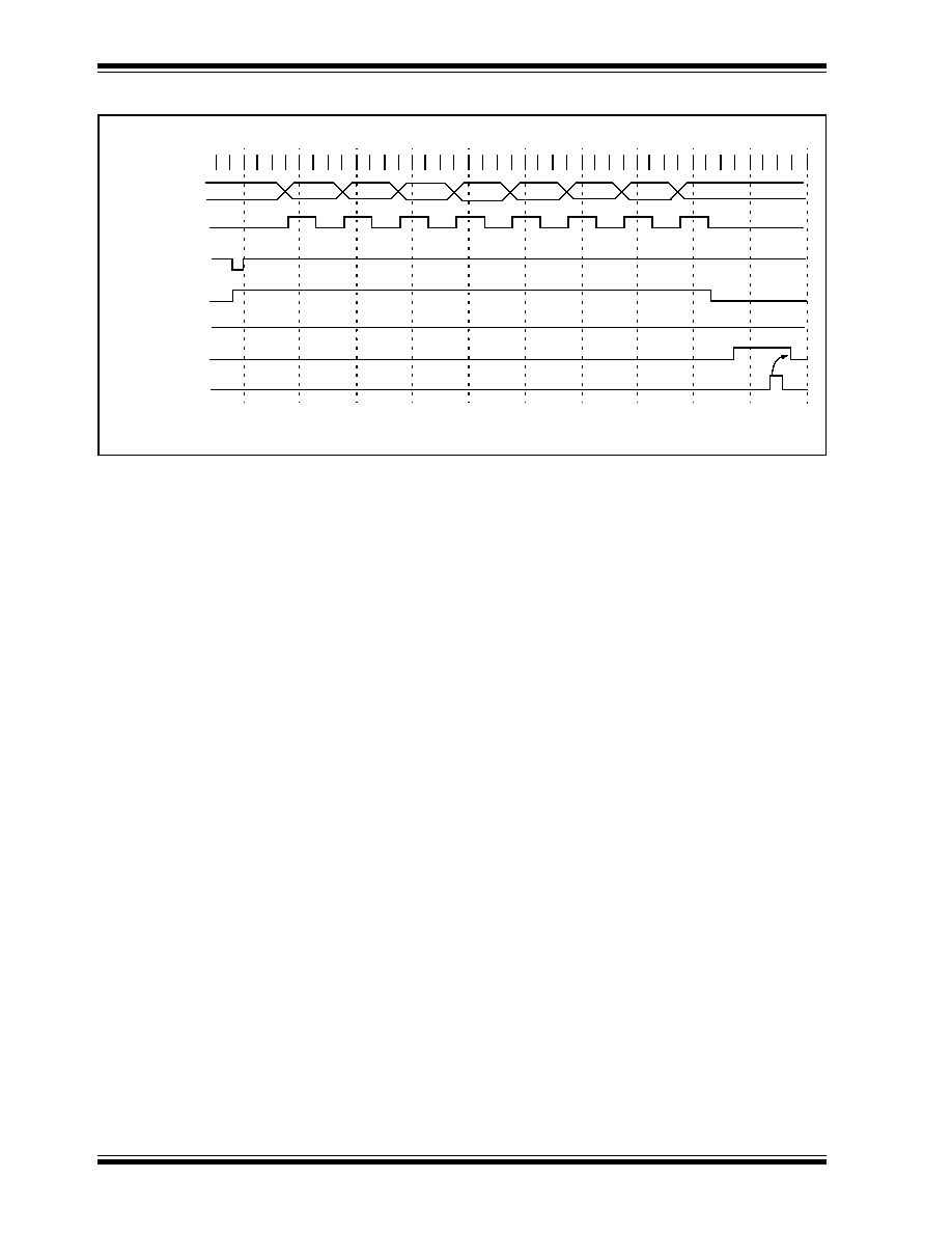
PIC18CXX2
DS39026B-page 164
Preliminary
©
7/99 Microchip Technology Inc.
FIGURE 15-8: SYNCHRONOUS RECEPTION (MASTER MODE, SREN)
CREN bit
RC7/RX/DT pin
RC6/TX/CK pin
Write to
bit SREN
SREN bit
RCIF bit
(interrupt)
Read
RXREG
Note: Timing diagram demonstrates SYNC master mode with bit SREN = '1' and bit BRGH = '0'.
Q3 Q4 Q1 Q2 Q3 Q4 Q1 Q2 Q3 Q4
Q2
Q1 Q2 Q3 Q4 Q1 Q2 Q3 Q4 Q1 Q2 Q3 Q4 Q1 Q2 Q3 Q4 Q1 Q2 Q3 Q4 Q1 Q2 Q3 Q4 Q1 Q2 Q3 Q4
'0'
bit0
bit1
bit2
bit3
bit4
bit5
bit6
bit7
'0'
Q1 Q2 Q3 Q4

PIC18CXX2
©
7/99 Microchip Technology Inc.
Preliminary
DS39026B-page 165
15.4
USART Synchronous Slave Mode
Synchronous Slave Mode differs from the Master Mode
in the fact that the shift clock is supplied externally at
the RC6/TX/CK pin (instead of being supplied internally
in master mode). This allows the device to transfer or
receive data while in SLEEP mode. Slave mode is
entered by clearing bit CSRC (TXSTA<7>).
15.4.1
USART SYNCHRONOUS SLAVE
TRANSMIT
The operation of the synchronous master and slave
modes are identical, except in the case of the SLEEP
mode.
If two words are written to the TXREG and then the
SLEEP instruction is executed, the following will occur:
a)
The first word will immediately transfer to the
TSR register and transmit.
b)
The second word will remain in TXREG register.
c)
Flag bit TXIF will not be set.
d)
When the first word has been shifted out of TSR,
the TXREG register will transfer the second
word to the TSR and flag bit TXIF will now be
set.
e)
If enable bit TXIE is set, the interrupt will wake
the chip from SLEEP. If the global interrupt is
enabled, the program will branch to the interrupt
vector.
Steps to follow when setting up a Synchronous Slave
Transmission:
1.
Enable the synchronous slave serial port by set-
ting bits SYNC and SPEN and clearing bit
CSRC.
2.
Clear bits CREN and SREN.
3.
If interrupts are desired, set enable bit TXIE.
4.
If 9-bit transmission is desired, set bit TX9.
5.
Enable the transmission by setting enable bit
TXEN.
6.
If 9-bit transmission is selected, the ninth bit
should be loaded in bit TX9D.
7.
Start transmission by loading data to the
TXREG register.
15.4.2
USART SYNCHRONOUS SLAVE
RECEPTION
The operation of the synchronous master and slave
modes is identical, except in the case of the SLEEP
mode and bit SREN, which is a "don't care" in slave
mode.
If receive is enabled by setting bit CREN prior to the
SLEEP instruction, then a word may be received during
SLEEP. On completely receiving the word, the RSR
register will transfer the data to the RCREG register,
and if enable bit RCIE bit is set, the interrupt generated
will wake the chip from SLEEP. If the global interrupt is
enabled, the program will branch to the interrupt vector.
Steps to follow when setting up a Synchronous Slave
Reception:
1.
Enable the synchronous master serial port by
setting bits SYNC and SPEN and clearing bit
CSRC.
2.
If interrupts are desired, set enable bit RCIE.
3.
If 9-bit reception is desired, set bit RX9.
4.
To enable reception, set enable bit CREN.
5.
Flag bit RCIF will be set when reception is com-
plete. An interrupt will be generated if enable bit
RCIE was set.
6.
Read the RCSTA register to get the ninth bit (if
enabled) and determine if any error occurred
during reception.
7.
Read the 8-bit received data by reading the
RCREG register.
8.
If any error occurred, clear the error by clearing
bit CREN.
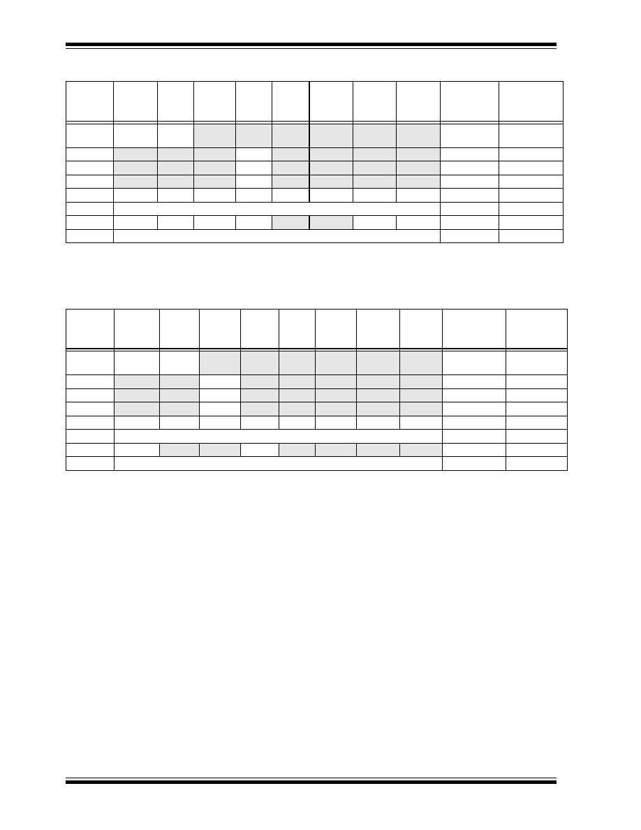
PIC18CXX2
DS39026B-page 166
Preliminary
©
7/99 Microchip Technology Inc.
TABLE 15-10: REGISTERS ASSOCIATED WITH SYNCHRONOUS SLAVE TRANSMISSION
TABLE 15-11: REGISTERS ASSOCIATED WITH SYNCHRONOUS SLAVE RECEPTION
Name
Bit 7
Bit 6
Bit 5
Bit 4
Bit 3
Bit 2
Bit 1
Bit 0
Value on
POR,
BOR
Value on all
other Resets
INTCON
GIE/
GIEH
PEIE/
GIEL
TMR0IE INT0IE
RBIE
TMR0IF
INT0IF
RBIF
0000 000x
0000 000u
PIR1
PSPIF
(1)
ADIF
RCIF
TXIF
SSPIF
CCP1IF
TMR2IF
TMR1IF
0000 0000
0000 0000
PIE1
PSPIE
(1)
ADIE
RCIE
TXIE
SSPIE
CCP1IE
TMR2IE
TMR1IE
0000 0000
0000 0000
IPR1
PSPIP
(1)
ADIP
RCIP
TXIP
SSPIP
CCP1IP
TMR2IP
TMR1IP
0000 0000
0000 0000
RCSTA
SPEN
RX9
SREN
CREN
--
FERR
OERR
RX9D
0000 -00x
0000 -00x
TXREG
USART Transmit Register
0000 0000
0000 0000
TXSTA
CSRC
TX9
TXEN
SYNC
--
BRGH
TRMT
TX9D
0000 -010
0000 -010
SPBRG
Baud Rate Generator Register
0000 0000
0000 0000
Legend: x = unknown, -- = unimplemented read as '0'.
Shaded cells are not used for Synchronous Slave Transmission.
Note 1: The PSPIF, PSPIE and PSPIP bits are reserved on the PIC18C2X2 devices. Always maintain these bits clear.
Name
Bit 7
Bit 6
Bit 5
Bit 4
Bit 3
Bit 2
Bit 1
Bit 0
Value on
POR,
BOR
Value on all
other
Resets
INTCON
GIE/
GIEH
PEIE/
GIEL
TMR0IE INT0IE
RBIE
TMR0IF
INT0IF
RBIF
0000 000x
0000 000u
PIR1
PSPIF
(1)
ADIF
RCIF
TXIF
SSPIF CCP1IF TMR2IF
TMR1IF
0000 0000
0000 0000
PIE1
PSPIE
(1)
ADIE
RCIE
TXIE
SSPIE CCP1IE TMR2IE TMR1IE
0000 0000
0000 0000
IPR1
PSPIP
(1)
ADIP
RCIP
TXIP
SSPIP CCP1IP TMR2IP TMR1IP
0000 0000
0000 0000
RCSTA
SPEN
RX9
SREN
CREN
--
FERR
OERR
RX9D
0000 -00x
0000 -00x
RCREG
USART Receive Register
0000 0000
0000 0000
TXSTA
CSRC
TX9
TXEN
SYNC
--
BRGH
TRMT
TX9D
0000 -010
0000 -010
SPBRG
Baud Rate Generator Register
0000 0000
0000 0000
Legend: x = unknown, -- = unimplemented read as '0'.
Shaded cells are not used for Synchronous Slave Reception.
Note 1: The PSPIF, PSPIE and PSPIP bits are reserved on the PIC18C2X2 devices. Always maintain these bits clear.

PIC18CXX2
©
7/99 Microchip Technology Inc.
Preliminary
DS39026B-page 167
16.0
10-BIT ANALOG-TO-DIGITAL
CONVERTER (A/D) MODULE
The analog-to-digital (A/D) converter module has five
inputs for the PIC18C2x2 devices and eight for the
PIC18C4x2 devices. This module has the ADCON0
and ADCON1 register definitions that are compatible
with the mid-range A/D module.
The A/D allows conversion of an analog input signal to
a corresponding 10-bit digital number.
The A/D module has four registers. These registers
are:
∑ A/D Result High Register (ADRESH)
∑ A/D Result Low Register (ADRESL)
∑ A/D Control Register 0 (ADCON0)
∑ A/D Control Register 1 (ADCON1)
The ADCON0 register, shown in Register 16-1, con-
trols the operation of the A/D module. The ADCON1
register, shown in Register 16-2, configures the func-
tions of the port pins.
Register 16-1: ADCON0 Register
R/W-0
R/W-0
R/W-0
R/W-0
R/W-0
R/W-0
U-0
R/W-0
ADCS1
ADCS0
CHS2
CHS1
CHS0
GO/DONE
--
ADON
bit 7
bit 0
bit 7:6
ADCS1:ADCS0: A/D Conversion Clock Select bits (shown in bold)
000
= F
OSC
/2
001
= F
OSC
/8
010
= F
OSC
/32
011
= F
RC
(clock derived from the internal A/D RC oscillator)
100
= F
OSC
/4
101
= F
OSC
/16
110
= F
OSC
/64
111
= F
RC
(clock derived from the internal A/D RC oscillator)
Note:
The ADCS2 bit is located in the ADCON1 register
bit 5:3
CHS2:CHS0: Analog Channel Select bits
000
= channel 0, (AN0)
001
= channel 1, (AN1)
010
= channel 2, (AN2)
011
= channel 3, (AN3)
100
= channel 4, (AN4)
101
= channel 5, (AN5)
110
= channel 6, (AN6)
111
= channel 7, (AN7)
Note:
The PIC18C2X2 devices do not implement the full 8 A/D channels, the unimple-
mented selections are reserved. Do not select any unimplemented channel.
bit 2
GO/DONE: A/D Conversion Status bit
When ADON = 1
1
= A/D conversion in progress (setting this bit starts the A/D conversion which is automatically
cleared by hardware when the A/D conversion is complete)
0
= A/D conversion not in progress
bit 1
Unimplemented: Read as '0'
bit 0
ADON: A/D On bit
1
= A/D converter module is powered up
0
= A/D converter module is shut off and consumes no operating current
Legend:
R = Readable bit
W = Writable bit
U = Unimplemented bit, read as `0'
- n = Value at POR reset
'1' = Bit is set
'0' = Bit is cleared
x = Bit is unknown

PIC18CXX2
DS39026B-page 168
Preliminary
©
7/99 Microchip Technology Inc.
Register 16-2: ADCON1 Register
R/W-0
R/W-0
U-0
U-0
R/W-0
R/W-0
R/W-0
R/W-0
ADFM
ADCS2
--
--
PCFG3
PCFG2
PCFG1
PCFG0
bit 7
bit 0
bit 7:6
Unimplemented: Read as '0'
bit 7
ADFM: A/D Result format select.
1
= Right justified. 6 Most Significant bits of ADRESH are read as '0'.
0
= Left justified. 6 Least Significant bits of ADRESL are read as '0'.
bit 6
ADCS2: A/D Conversion Clock Select bit (shown in bold)
000
= F
OSC
/2
001
= F
OSC
/8
010
= F
OSC
/32
011
= F
RC
(clock derived from the internal A/D RC oscillator)
100
= F
OSC
/4
101
= F
OSC
/16
110
= F
OSC
/64
111
= F
RC
(clock derived from the internal A/D RC oscillator)
Note:
The ADCS1:ADCS0 bits are located in the ADCON0 register
bit 5:4
Unimplemented: Read as '0'
bit 3:0
PCFG3:PCFG0: A/D Port Configuration Control bits
Legend:
R = Readable bit
W = Writable bit
U = Unimplemented bit, read as `0'
- n = Value at POR reset
'1' = Bit is set
'0' = Bit is cleared
x = Bit is unknown
Note:
On any device reset, the port pins that are multiplexed with analog functions (ANx) are
forced to be an analog input.
A = Analog input D = Digital I/O
C/R = # of analog input channels / # of A/D voltage references
PCFG
AN7
AN6
AN5
AN4
AN3
AN2
AN1
AN0
V
REF
+
V
REF
-
C / R
0000
A
A
A
A
A
A
A
A
V
DD
V
SS
8 / 0
0001
A
A
A
A
V
REF
+
A
A
A
AN3
V
SS
7 / 1
0010
D
D
D
A
A
A
A
A
V
DD
V
SS
5 / 0
0011
D
D
D
A
V
REF
+
A
A
A
AN3
V
SS
4 / 1
0100
D
D
D
D
A
D
A
A
V
DD
V
SS
3 / 0
0101
D
D
D
D
V
REF
+
D
A
A
AN3
V
SS
2 / 1
011x
D
D
D
D
D
D
D
D
--
--
0 / 0
1000
A
A
A
A
V
REF
+
V
REF
-
A
A
AN3
AN2
6 / 2
1001
D
D
A
A
A
A
A
A
V
DD
V
SS
6 / 0
1010
D
D
A
A
V
REF
+
A
A
A
AN3
V
SS
5 / 1
1011
D
D
A
A
V
REF
+
V
REF
-
A
A
AN3
AN2
4 / 2
1100
D
D
D
A
V
REF
+
V
REF
-
A
A
AN3
AN2
3 / 2
1101
D
D
D
D
V
REF
+
V
REF
-
A
A
AN3
AN2
2 / 2
1110
D
D
D
D
D
D
D
A
V
DD
V
SS
1 / 0
1111
D
D
D
D
V
REF
+
V
REF
-
D
A
AN3
AN2
1 / 2
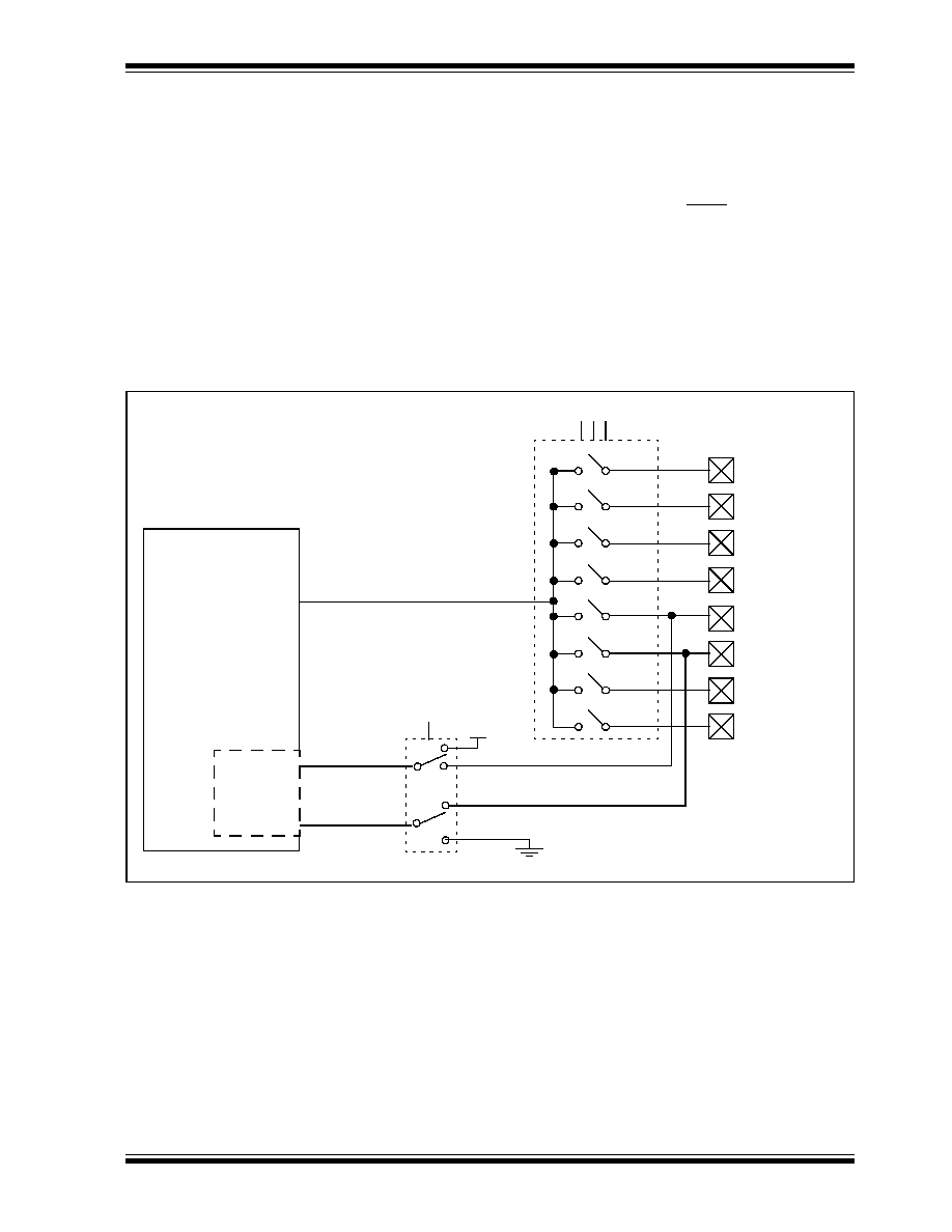
PIC18CXX2
©
7/99 Microchip Technology Inc.
Preliminary
DS39026B-page 169
The analog reference voltage is software selectable to
either the device's positive and negative supply voltage
(V
DD
and V
SS
) or the voltage level on the RA3/AN3/
V
REF
+ pin and RA2/AN2/V
REF
-.
The A/D converter has a unique feature of being able to
operate while the device is in SLEEP mode. To operate
in sleep, the A/D conversion clock must be derived from
the A/D's internal RC oscillator.
The output of the sample and hold is the input into the
converter, which generates the result via successive
approximation.
A device reset forces all registers to their reset state.
This forces the A/D module to be turned off and any
conversion is aborted.
Each port pin associated with the A/D converter can
be configured as an analog input (RA3 can also be a
voltage reference) or as a digital I/O.
The ADRESH and ADRESL registers contain the result
of the A/D conversion. When the A/D conversion is
complete, the result is loaded into the ADRESH/
ADRESL registers, the GO/DONE bit (ADCON0<2>) is
cleared, and A/D interrupt flag bit ADIF is set. The block
diagram of the A/D module is shown in Figure 16-1.
FIGURE 16-1: A/D BLOCK DIAGRAM
(Input voltage)
V
AIN
V
REF
+
Reference
voltage
V
DD
PCFG0
CHS2:CHS0
AN7
AN6
AN5
AN4
AN3
AN2
AN1
AN0
111
110
101
100
011
010
001
000
10-bit
Converter
V
REF
-
V
SS
A/D
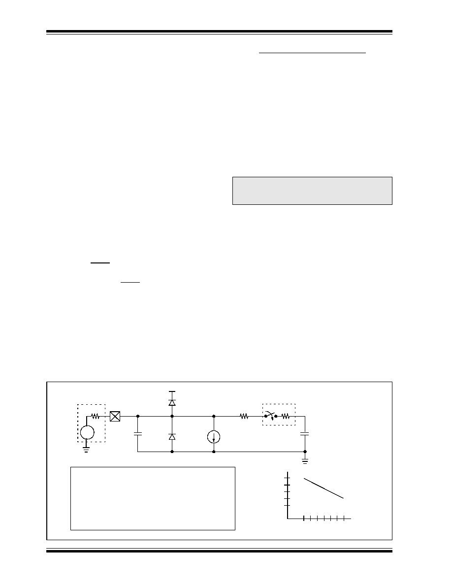
PIC18CXX2
DS39026B-page 170
Preliminary
©
7/99 Microchip Technology Inc.
The value that is in the ADRESH/ADRESL registers is
not modified for a Power-on Reset. The ADRESH/
ADRESL registers will contain unknown data after a
Power-on Reset.
After the A/D module has been configured as desired,
the selected channel must be acquired before the con-
version is started. The analog input channels must
have their corresponding TRIS bits selected as an
input. To determine acquisition time, see Section 16.1.
After this acquisition time has elapsed, the A/D conver-
sion can be started. The following steps should be fol-
lowed for doing an A/D conversion:
1.
Configure the A/D module:
∑ Configure analog pins, voltage reference and
digital I/O (ADCON1)
∑ Select A/D input channel (ADCON0)
∑ Select A/D conversion clock (ADCON0)
∑ Turn on A/D module (ADCON0)
2.
Configure A/D interrupt (if desired):
∑ Clear ADIF bit
∑ Set ADIE bit
∑ Set GIE bit
3.
Wait the required acquisition time.
4.
Start conversion:
∑ Set GO/DONE bit (ADCON0)
5.
Wait for A/D conversion to complete, by either:
∑ Polling for the GO/DONE bit to be cleared
OR
∑ Waiting for the A/D interrupt
6.
Read A/D Result registers (ADRESH/ADRESL);
clear bit ADIF if required.
7.
For next conversion, go to step 1 or step 2 as
required. The A/D conversion time per bit is
defined as T
AD
. A minimum wait of 2T
AD
is
required before next acquisition starts.
16.1
A/D Acquisition Requirements
For the A/D converter to meet its specified accuracy,
the charge holding capacitor (C
HOLD
) must be allowed
to fully charge to the input channel voltage level. The
analog input model is shown in Figure 16-2. The
source impedance (R
S
) and the internal sampling
switch (R
SS
) impedance directly affect the time
required to charge the capacitor C
HOLD
. The sampling
switch (R
SS
) impedance varies over the device voltage
(V
DD
). The source impedance affects the offset voltage
at the analog input (due to pin leakage current). The
maximum recommended impedance for analog
sources is 2.5k
. After the analog input channel is
selected (changed), this acquisition must be done
before the conversion can be started.
FIGURE 16-2: ANALOG INPUT MODEL
Note:
When the conversion is started, the hold-
ing capacitor is disconnected from the
input pin.
V
AIN
C
PIN
Rs
ANx
5 pF
V
DD
V
T
= 0.6V
V
T
= 0.6V
I leakage
R
IC
1k
Sampling
Switch
SS
R
SS
C
HOLD
= 120 pF
V
SS
6V
Sampling Switch
5V
4V
3V
2V
5 6 7 8 9 10 11
( k
)
V
DD
± 500 nA
Legend: C
PIN
V
T
I
LEAKAGE
R
IC
SS
C
HOLD
= input capacitance
= threshold voltage
= leakage current at the pin due to
= interconnect resistance
= sampling switch
= sample/hold capacitance (from DAC)
various junctions

PIC18CXX2
©
7/99 Microchip Technology Inc.
Preliminary
DS39026B-page 171
To calculate the minimum acquisition time,
Equation 16-1 may be used. This equation assumes
that 1/2 LSb error is used (1024 steps for the A/D). The
1/2 LSb error is the maximum error allowed for the A/D
to meet its specified resolution.
Equation 16-1: Acquisition Time
Equation 16-2: A/D Minimum Charging Time
Example 16-3 shows the calculation of the minimum
required acquisition time T
ACQ
. This calculation is
based on the following application system assump-
tions:
C
HOLD
=
120
pF
Rs
=
2.5 k
Conversion Error
1/2 LSb
V
DD
=
5V
Rss = 7 k
Temperature
=
50
∞
C (system max.)
V
HOLD
=
0V @ time = 0
EXAMPLE 16-3: CALCULATING THE MINIMUM REQUIRED ACQUISITION TIME
T
ACQ
=
Amplifier Settling Time +
Holding Capacitor Charging Time +
Temperature Coefficient
=
T
AMP
+ T
C
+ T
COFF
V
HOLD
=
(V
REF
- (V
REF
/2048)) ∑ (1 - e
(-Tc/C
HOLD
(R
IC
+ R
SS
+ R
S
))
)
or
Tc =
-(120
pF)(1
k
+ R
SS
+ R
S
) ln(1/2047)
T
ACQ
=
T
AMP
+ T
C
+ T
COFF
Temperature coefficient is only required for temperatures > 25
∞
C.
T
ACQ
=
2
µ
s + Tc + [(Temp - 25
∞
C)(0.05
µ
s/
∞
C)]
T
C
=
-C
HOLD
(R
IC
+ R
SS
+ R
S
) ln(1/2047)
-120 pF (1 k
+ 7 k
+ 2.5 k
) ln(0.0004885)
-120 pF (10.5 k
) ln(0.0004885)
-1.26
µ
s (-7.6241)
9.61
µ
s
T
ACQ
=
2
µ
s + 9.61
µ
s + [(50
∞
C - 25
∞
C)(0.05
µ
s/
∞
C)]
11.61
µ
s + 1.25
µ
s
12.86
µ
s
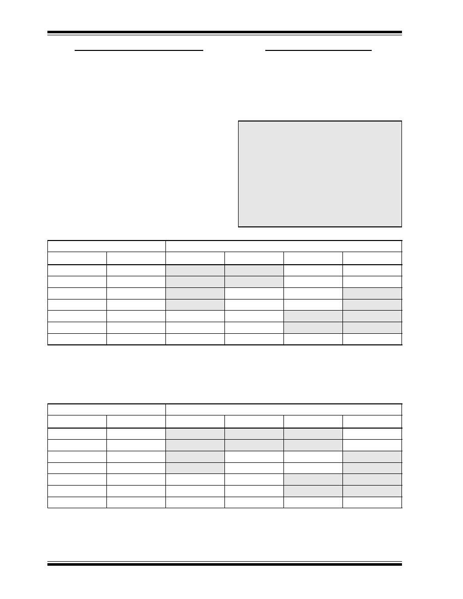
PIC18CXX2
DS39026B-page 172
Preliminary
©
7/99 Microchip Technology Inc.
16.2
Selecting the A/D Conversion Clock
The A/D conversion time per bit is defined as T
AD
. The
A/D conversion requires 12 T
AD
per 10-bit conversion.
The source of the A/D conversion clock is software
selectable. The seven possible options for T
AD
are:
∑ 2T
OSC
∑ 4T
OSC
∑ 8T
OSC
∑ 16T
OSC
∑ 32T
OSC
∑ 64T
OSC
∑ Internal RC oscillator
For correct A/D conversions, the A/D conversion clock
(T
AD
) must be selected to ensure a minimum T
AD
time
of 1.6
µ
s.
Table 16-1 shows the resultant T
AD
times derived from
the device operating frequencies and the A/D clock
source selected.
16.3
Configuring Analog Port Pins
The ADCON1, TRISA and TRISE registers control the
operation of the A/D port pins. The port pins that are
desired as analog inputs must have their corresponding
TRIS bits set (input). If the TRIS bit is cleared (output),
the digital output level (V
OH
or V
OL
) will be converted.
The A/D operation is independent of the state of the
CHS2:CHS0 bits and the TRIS bits.
TABLE 16-1:
T
AD
vs. DEVICE OPERATING FREQUENCIES
TABLE 16-2:
T
AD
vs. DEVICE OPERATING FREQUENCIES (FOR EXTENDED, LC, DEVICES)
Note 1: When reading the port register, all pins
configured as analog input channels will
read as cleared (a low level). Pins config-
ured as digital inputs will convert an ana-
log input. Analog levels on a digitally
configured input will not affect the conver-
sion accuracy.
Note 2: Analog levels on any pin that is defined as
a digital input (including the AN4:AN0
pins) may cause the input buffer to con-
sume current that is out of the devices
specification.
AD Clock Source (T
AD
)
Device Frequency
Operation
ADCS2:ADCS0
20 MHz
5 MHz
1.25 MHz
333.33 kHz
2T
OSC
000
100 ns
(2)
400 ns
(2)
1.6
µ
s
6
µ
s
4T
OSC
100
200 ns
(2)
800 ns
(2)
3.2
µ
s
12
µ
s
8T
OSC
001
400 ns
(2)
1.6
µ
s
6.4
µ
s
24
µ
s
(3)
16T
OSC
101
800 ns
(2)
3.2
µ
s
12.8
µ
s
48
µ
s
(3)
32T
OSC
010
1.6
µ
s
6.4
µ
s
25.6
µ
s
(3)
96
µ
s
(3)
64T
OSC
110
3.2
µ
s
12.8
µ
s
51.2
µ
s
(3)
192
µ
s
(3)
RC
011
2 - 6
µ
s
(1,4)
2 - 6
µ
s
(1,4)
2 - 6
µ
s
(1,4)
2 - 6
µ
s
(1)
Legend: Shaded cells are outside of recommended range.
Note 1: The RC source has a typical T
AD
time of 4
µ
s.
2: These values violate the minimum required T
AD
time.
3: For faster conversion times, the selection of another clock source is recommended.
4: For device frequencies above 1 MHz, the device must be in SLEEP for the entire conversion or the A/D accuracy may be
out of specification.
AD Clock Source (T
AD
)
Device Frequency
Operation
ADCS2:ADCS0
4 MHz
2 MHz
1.25 MHz
333.33 kHz
2T
OSC
000
500 ns
(2)
1.0
µ
s
(2)
1.6
µ
s
(2)
6
µ
s
4T
OSC
100
1.0
µ
s
(2)
2.0
µ
s
(2)
3.2
µ
s
(2)
12
µ
s
8T
OSC
001
2.0
µ
s
(2)
4.0
µ
s
6.4
µ
s
24
µ
s
(3)
16T
OSC
101
4.0
µ
s
(2)
8.0
µ
s
12.8
µ
s
48
µ
s
(3)
32T
OSC
010
8.0
µ
s
16.0
µ
s
25.6
µ
s
(3)
96
µ
s
(3)
64T
OSC
110
16.0
µ
s
32.0
µ
s
51.2
µ
s
(3)
192
µ
s
(3)
RC
011
3 - 9
µ
s
(1,4)
3 - 9
µ
s
(1,4)
3 - 9
µ
s
(1,4)
3 - 9
µ
s
(1,4)
Legend: Shaded cells are outside of recommended range.
Note 1: The RC source has a typical T
AD
time of 6
µ
s.
2: These values violate the minimum required T
AD
time.
3: For faster conversion times, the selection of another clock source is recommended.
4: For device frequencies above 1 MHz, the device must be in SLEEP for the entire conversion or the A/D accuracy may be
out of specification.
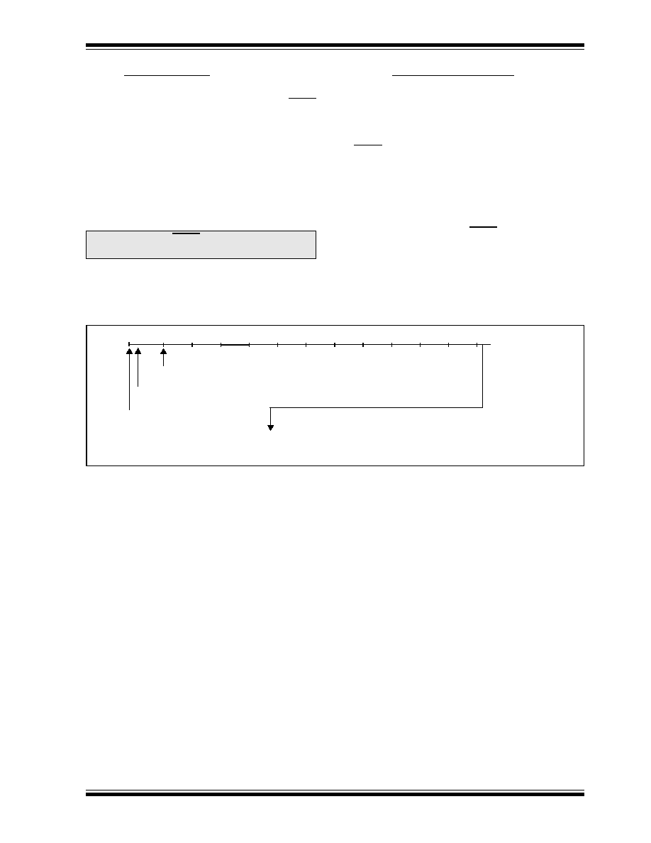
PIC18CXX2
©
7/99 Microchip Technology Inc.
Preliminary
DS39026B-page 173
16.4
A/D Conversions
Figure 16-3 shows the operation of the A/D converter
after the GO bit has been set. Clearing the GO/DONE
bit during a conversion will abort the current conver-
sion. The A/D result register pair will NOT be updated
with the partially completed A/D conversion sample.
That is, the ADRESH:ADRESL registers will continue
to contain the value of the last completed conversion
(or the last value written to the ADRESH:ADRESL reg-
isters). After the A/D conversion is aborted, a 2T
AD
wait
is required before the next acquisition is started. After
this 2T
AD
wait, acquisition on the selected channel is
automatically started.
16.5
Use of the CCP2 Trigger
An A/D conversion can be started by the "special event
trigger" of the CCP2 module. This requires that the
CCP2M3:CCP2M0 bits (CCP2CON<3:0>) be pro-
grammed as
1011
and that the A/D module is enabled
(ADON bit is set). When the trigger occurs, the GO/
DONE bit will be set, starting the A/D conversion, and
the Timer1 (or Timer3) counter will be reset to zero.
Timer1 (or Timer3) is reset to automatically repeat the
A/D acquisition period with minimal software overhead
(moving ADRESH/ADRESL to the desired location).
The appropriate analog input channel must be selected
and the minimum acquisition done before the "special
event trigger" sets the GO/DONE bit (starts a conver-
sion).
If the A/D module is not enabled (ADON is cleared), the
"special event trigger" will be ignored by the A/D mod-
ule, but will still reset the Timer1 (or Timer3) counter.
FIGURE 16-3: A/D CONVERSION T
AD
CYCLES
Note:
The GO/DONE bit should NOT be set in
the same instruction that turns on the A/D.
T
AD
1 T
AD
2 T
AD
3 T
AD
4 T
AD
5 T
AD
6 T
AD
7 T
AD
8
T
AD
11
Set GO bit
Holding capacitor is disconnected from analog input (typically 100 ns)
b9
b8
b7
b6
b5
b4
b3
b2
T
AD
9 T
AD
10
b1
b0
Tcy - T
AD
Next Q4: ADRESH/ADRESL is loaded, GO bit is cleared,
ADIF bit is set, holding capacitor is connected to analog input.
Conversion Starts
b0
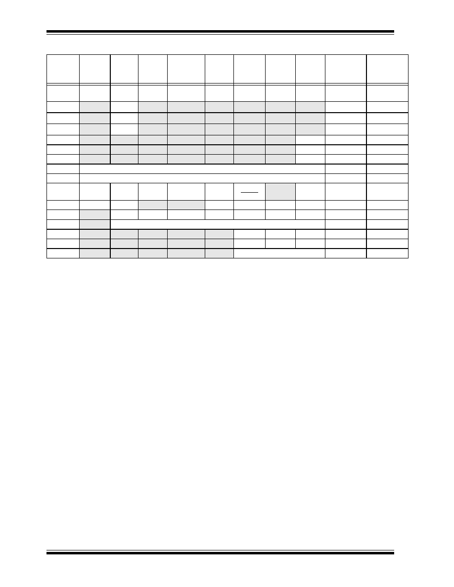
PIC18CXX2
DS39026B-page 174
Preliminary
©
7/99 Microchip Technology Inc.
TABLE 16-3:
SUMMARY OF A/D REGISTERS
Name
Bit 7
Bit 6
Bit 5
Bit 4
Bit 3
Bit 2
Bit 1
Bit 0
Value on
POR, BOR
Value on
all other
Resets
INTCON
GIE/
GIEH
PEIE/
GIEL
TMR0IE
INT0IE
RBIE
TMR0IF
INT0IF
RBIF
0000 000x
0000 000u
PIR1
PSPIF
(1)
ADIF
RCIF
TXIF
SSPIF
CCP1IF
TMR2IF
TMR1IF
0000 0000
0000 0000
PIE1
PSPIE
(1)
ADIE
RCIE
TXIE
SSPIE
CCP1IE
TMR2IE
TMR1IE
0000 0000
0000 0000
IPR1
PSPIP
(1)
ADIP
RCIP
TXIP
SSPIP
CCP1IP
TMR2IP
TMR1IP
0000 0000
0000 0000
PIR2
--
--
--
--
BCLIF
LVDIF
TMR3IF
CCP2IF
---- 0000
---- 0000
PIE2
--
--
--
--
BCLIE
LVDIE
TMR3IE
CCP2IE
---- 0000
---- 0000
IPR2
--
--
--
--
BCLIP
LVDIP
TMR3IP
CCP2IP
---- 0000
---- 0000
ADRESH
A/D Result Register
xxxx xxxx
uuuu uuuu
ADRESL
A/D Result Register
xxxx xxxx
uuuu uuuu
ADCON0
ADCS1
ADCS0
CHS2
CHS1
CHS0
GO/
DONE
--
ADON
0000 00-0
0000 00-0
ADCON1
ADFM
ADCS2
--
--
PCFG3
PCFG2
PCFG1
PCFG0
---- -000
---- -000
PORTA
--
RA6
RA5
RA4
RA3
RA2
RA1
RA0
--0x 0000
--0u 0000
TRISA
--
PORTA Data Direction Register
--11 1111
--11 1111
PORTE
--
--
--
--
--
RE2
RE1
RE0
---- -000
---- -000
LATE
--
--
--
--
--
LATE2
LATE1
LATE0
---- -xxx
---- -uuu
TRISE
IBF
OBF
IBOV
PSPMODE
--
PORTE Data Direction Bits
0000 -111
0000 -111
Legend: x = unknown, u = unchanged,
--
= unimplemented read as '0'. Shaded cells are not used for A/D conversion.
Note 1: The PSPIF, PSPIE and PSPIP bits are reserved on the PIC18C2X2 devices. Always maintain these bits clear.
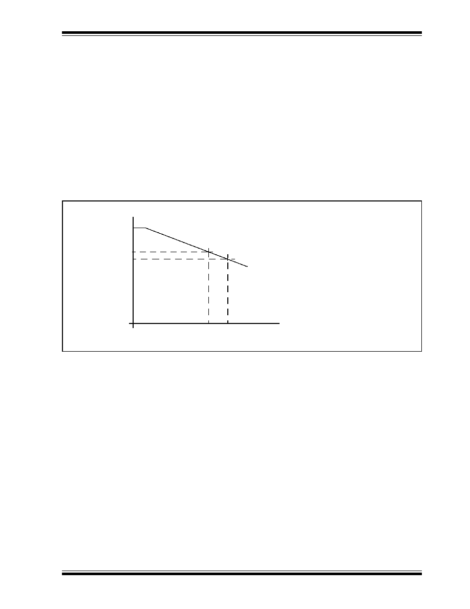
PIC18CXX2
©
7/99 Microchip Technology Inc.
Preliminary
DS39026B-page 175
17.0
LOW VOLTAGE DETECT
In many applications, the ability to determine if the
device voltage (V
DD
) is below a specified voltage level
is a desirable feature. A window of operation for the
application can be created, where the application soft-
ware can do "housekeeping tasks" before the device
voltage exits the valid operating range. This can be
done using the Low Voltage Detect module.
This module is a software programmable circuitry,
where a device voltage trip point can be specified.
When the voltage of the device becomes lower then the
specified point, an interrupt flag is set. If the interrupt is
enabled, the program execution will branch to the inter-
rupt vector address and the software can then respond
to that interrupt source.
The Low Voltage Detect circuitry is completely under
software control. This allows the circuitry to be "turned
off" by the software, which minimizes the current con-
sumption for the device.
Figure 17-1 shows a possible application voltage curve
(typically for batteries). Over time, the device voltage
decreases. When the device voltage equals voltage V
A
,
the LVD logic generates an interrupt. This occurs at
time T
A
. The application software then has the time until
the device voltage is no longer in valid operating range
to shut down the system. Voltage point V
B
is the mini-
mum valid operating voltage specification. This occurs
at time T
B
. T
B
- T
A
is the total time for shutdown.
FIGURE 17-1: TYPICAL LOW VOLTAGE DETECT APPLICATION
Time
Vo
l
t
a
g
e
V
A
V
B
T
A
T
B
V
A
= LVD trip point
V
B
= Minimum valid device
operating voltage
Legend:
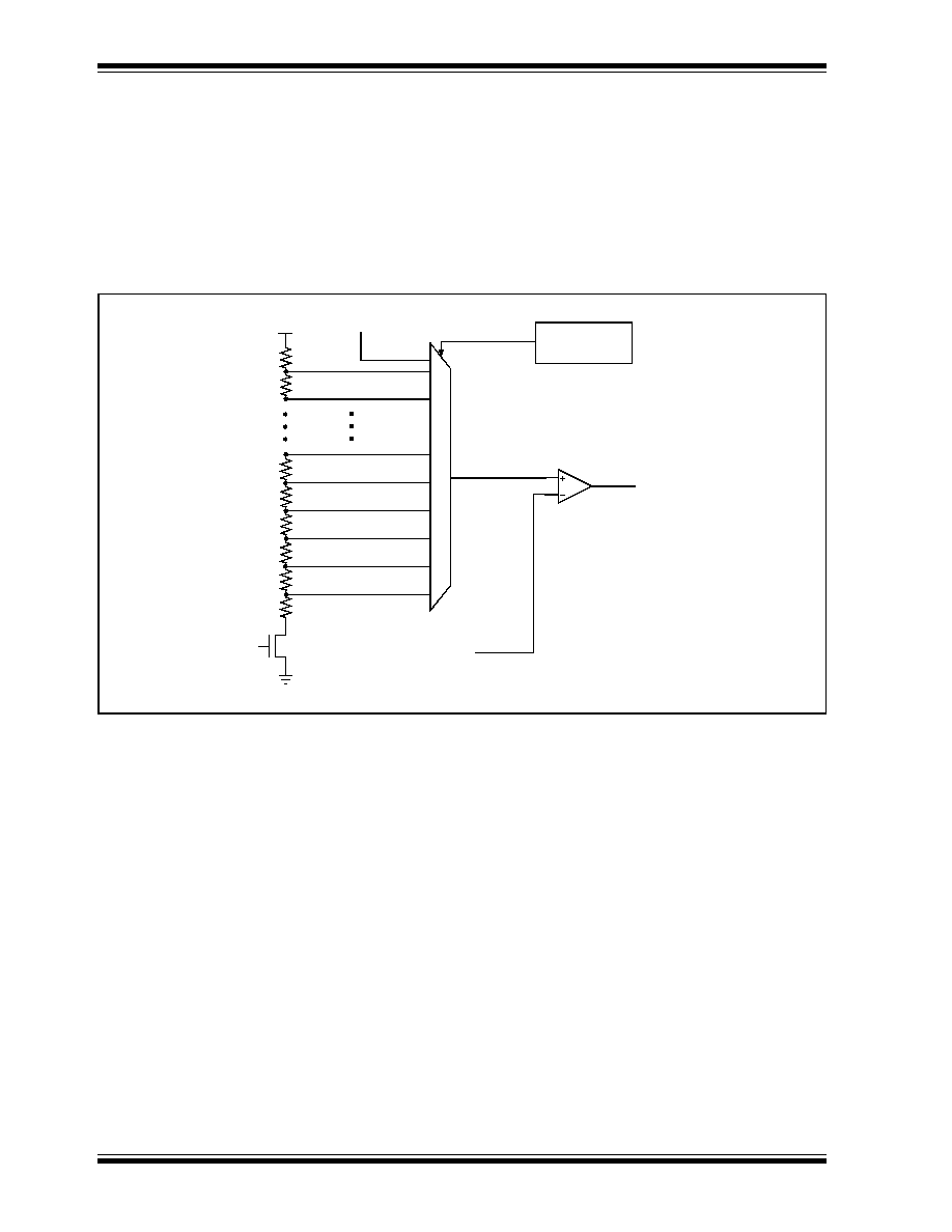
PIC18CXX2
DS39026B-page 176
Preliminary
©
7/99 Microchip Technology Inc.
Figure 17-2 shows the block diagram for the LVD mod-
ule. A comparator uses an internally generated refer-
ence voltage as the set point. When the selected tap
output of the device voltage crosses the set point (is
lower than), the LVDIF bit is set.
Each node in the resister divider represents a "trip
point" voltage. The "trip point" voltage is the minimum
supply voltage level at which the device can operate
before the LVD module asserts an interrupt. When the
supply voltage is equal to the trip point, the voltage
tapped off of the resistor array is equal to the voltage
generated by the internal voltage reference module.
The comparator then generates an interrupt signal set-
ting the LVDIF bit. This voltage is software programma-
ble to any one of 16 values (See Figure 17-2). The trip
point is selected by programming the LVDL3:LVDL0
bits (LVDCON<3:0>).
FIGURE 17-2: LOW VOLTAGE DETECT (LVD) BLOCK DIAGRAM
LVDIF
V
DD
16
t
o
1
MU
X
LVDEN
LVD Control
Register
Internally generated
reference voltage
LVDIN

PIC18CXX2
©
7/99 Microchip Technology Inc.
Preliminary
DS39026B-page 177
17.1
Control Register
The Low Voltage Detect Control register controls the
operation of the Low Voltage Detect circuitry.
Register 17-1: LVDCON Register
U-0
U-0
R-0
R/W-0
R/W-0
R/W-1
R/W-0
R/W-1
--
--
IRVST
LVDEN
LVDL3
LVDL2
LVDL1
LVDL0
bit 7
bit 0
bit 7:6
Unimplemented: Read as '0'
bit 5
IRVST: Internal Reference Voltage Stable Flag bit
1
= Indicates that the Low Voltage Detect logic will generate the interrupt flag at the
specified voltage range.
0
= Indicates that the Low Voltage Detect logic will not generate the interrupt flag at the
specified voltage range and the LVD interrupt should not be enabled
bit 4
LVDEN: Low-voltage Detect Power Enable bit
1
= Enables LVD, powers up LVD circuit
0
= Disables LVD, powers down LVD circuit
bit 3:0
LVDL3:LVDL0: Low Voltage Detection Limit bits
1111
= External analog input is used (input comes from the LVDIN pin)
1110
= 4.5V min - 4.77V max.
1101
= 4.2V min - 4.45V max.
1100
= 4.0V min - 4.24V max.
1011
= 3.8V min - 4.03V max.
1010
= 3.6V min - 3.82V max.
1001
= 3.5V min - 3.71V max.
1000
= 3.3V min - 3.50V max.
0111
= 3.0V min - 3.18V max.
0110
= 2.8V min - 2.97V max.
0101
= 2.7V min - 2.86V max.
0100
= 2.5V min - 2.65V max.
0011
= 2.4V min - 2.54V max.
0010
= 2.2V min - 2.33V max.
0001
= 2.0V min - 2.12V max.
0000
= 1.8V min - 1.91V max.
Note:
LVDL3:LVDL0 modes which result in a trip point below the valid operating voltage
of the device are not tested.
Legend:
R = Readable bit
W = Writable bit
U = Unimplemented bit, read as `0'
- n = Value at POR reset
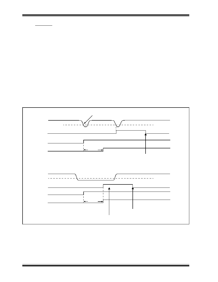
PIC18CXX2
DS39026B-page 178
Preliminary
©
7/99 Microchip Technology Inc.
17.2
Operation
Depending on the power source for the device voltage,
the voltage normally decreases relatively slowly. This
means that the LVD module does not need to be con-
stantly operating. To decrease the current require-
ments, the LVD circuitry only needs to be enabled for
short periods, where the voltage is checked. After
doing the check, the LVD module may be disabled.
Each time that the LVD module is enabled, the circuitry
requires some time to stabilize. After the circuitry has
stabilized, all status flags may be cleared. The module
will then indicate the proper state of the system.
The following steps are needed to setup the LVD
module:
1.
Write the value to the LVDL3:LVDL0 bits (LVD-
CON register), which selects the desired LVD
Trip Point.
2.
Ensure that LVD interrupts are disabled (the
LVDIE bit is cleared or the GIE bit is cleared).
3.
Enable the LVD module (Set the LVDEN bit in
the LVDCON register).
4.
Wait for the LVD module to stabilize (the IRVST
bit to become set).
5.
Clear the LVD interrupt flag, which may have
falsely become set until the LVD module has sta-
bilized (clear the LVDIF bit).
6.
Enable the LVD interrupt (set the LVDIE and the
GIE bits).
Figure 17-3 shows typical waveforms that the LVD
module may be used to detect.
FIGURE 17-3: LOW VOLTAGE DETECT WAVEFORMS
.
V
LVD
V
DD
LVDIF
V
LVD
V
DD
Enable LVD
Internally Generated
50 ms
LVDIF may not be set
Enable LVD
50 ms
LVDIF
LVDIF cleared in software
LVDIF cleared in software
LVDIF cleared in software,
CASE 1:
CASE 2:
LVDIF remains set since LVD condition still exists
Reference stable
Internally Generated
Reference stable

PIC18CXX2
©
7/99 Microchip Technology Inc.
Preliminary
DS39026B-page 179
17.2.1
REFERENCE VOLTAGE SET POINT
The Internal Reference Voltage of the LVD module may
be used by other internal circuitry (the programmable
brown-out reset). If these circuits are disabled (lower
current consumption), the reference voltage circuit
requires a time to become stable before a low voltage
condition can be reliably detected. This time is invariant
of system clock speed. This start-up time is specified in
electrical specification parameter #36. The low-voltage
interrupt flag will not be enabled until a stable reference
voltage is reached. Refer to the waveform in Figure 17-
3.
17.2.2
CURRENT CONSUMPTION
When the module is enabled, the LVD comparator and
voltage divider are enabled and will consume static cur-
rent. The voltage divider can be tapped from multiple
places in the resistor array. Total current consumption,
when enabled, is specified in electrical specification
parameter #D022B.
17.3
Operation During Sleep
When enabled, the LVD circuitry continues to operate
during sleep. If the device voltage crosses the trip point,
the LVDIF bit will be set and the device will wake-up
from sleep. Device execution will continue from the
interrupt vector address if interrupts have been globally
enabled.
17.4
Effects of a Reset
A device reset forces all registers to their reset state.
This forces the LVD module to be turned off.

PIC18CXX2
DS39026B-page 180
Preliminary
©
7/99 Microchip Technology Inc.
NOTES:

PIC18CXX2
©
7/99 Microchip Technology Inc.
Preliminary
DS39026B-page 181
18.0
SPECIAL FEATURES OF THE
CPU
There are several features intended to maximize sys-
tem reliability, minimize cost through elimination of
external components, provide power saving operating
modes and offer code protection. These are:
∑ OSC Selection
∑ Reset
- Power-on Reset (POR)
- Power-up Timer (PWRT)
- Oscillator Start-up Timer (OST)
- Brown-out Reset (BOR)
∑ Interrupts
∑ Watchdog Timer (WDT)
∑ SLEEP
∑ Code protection
∑ ID locations
∑ In-circuit serial programming
These devices have a Watchdog Timer, which is per-
manently enabled via the configuration bits or software-
controlled. It runs off its own RC oscillator for added
reliability. There are two timers that offer necessary
delays on power-up. One is the Oscillator Start-up
Timer (OST), intended to keep the chip in reset until the
crystal oscillator is stable. The other is the Power-up
Timer (PWRT), which provides a fixed delay on power-
up only, designed to keep the part in reset while the
power supply stabilizes. With these two timers on-chip,
most applications need no external reset circuitry.
SLEEP mode is designed to offer a very low current
power-down mode. The user can wake-up from SLEEP
through external reset, Watchdog Timer Wake-up or
through an interrupt. Several oscillator options are also
made available to allow the part to fit the application.
The RC oscillator option saves system cost, while the
LP crystal option saves power. A set of configuration
bits are used to select various options.
18.1
Configuration Bits
The configuration bits can be programmed (read as '0')
or left unprogrammed (read as '1') to select various
device configurations. These bits are mapped starting
at program memory location 300000h.
The user will note that address 300000h is beyond the
user program memory space. In fact, it belongs to the
configuration memory space (300000h - 3FFFFFh),
which can only be accessed using table reads and
table writes.
TABLE 18-1:
CONFIGURATION BITS AND DEVICE IDS
Filename
Bit 7
Bit 6
Bit 5
Bit 4
Bit 3
Bit 2
Bit 1
Bit 0
Default/
unprogrammed
value
300000h
CONFIG1L
CP
CP
CP
CP
CP
CP
CP
CP
1111 1111
300001h
CONFIG1H
--
--
OSCSEN
--
--
FOSC2
FOSC1
FOSC0
111- -111
300002h
CONFIG2L
--
--
--
--
BORV1
BORV0
BODEN
PWRTEN
---- 1111
300003h
CONFIG2H
--
--
--
--
WDTPS2
WDTPS1
WDTPS0
WDTEN
---- 1111
300005h
CONFIG3H
--
--
--
--
--
--
--
CCP2MX
---- ---1
300006h
CONFIG4L
--
--
--
--
--
--
LVEN
STVREN
---- --11
3FFFFEh
DEVID1
DEV2
DEV1
DEV0
REV4
REV3
REV2
REV1
REV0
0000 0000
3FFFFFh
DEVID2
DEV10
DEV9
DEV8
DEV7
DEV6
DEV5
DEV4
DEV3
0000 0010
Legend:
x = unknown, u = unchanged, - = unimplemented, q = value depends on condition, grayed cells are unimplemented read as 0

PIC18CXX2
DS39026B-page 182
Preliminary
©
7/99 Microchip Technology Inc.
Register 18-1: Configuration Register 1 High (CONFIG1H: Byte Address 300001h)
Register 18-2: Configuration Register 1 Low (CONFIG1L: Byte Address 300000h)
R/P-1
R/P-1
R/P-1
U-0
U-0
R/P-1
R/P-1
R/P-1
Reserved
Reserved
OSCSEN
--
--
FOSC2
FOSC1
FOSC0
bit 7
bit 0
bit 7-6
Reserved: Read as '1'
bit 5
OSCSEN: Oscillator System Clock Switch Enable bit
1
= Oscillator system clock switch option is disabled (Main oscillator is source)
0
= Oscillator system clock switch option is enabled
(Oscillator switching is enabled)
bit 4-3
Reserved: Read as '0'
bit 2-0
FOSC2:FOSC0: Oscillator Selection bits
111
= RC oscillator w/ OSC2 configured as RA6
110
= HS oscillator with PLL enabled/CLock frequency = (4 x Fosc)
101
= EC oscillator w/ OSC2 configured as RA6
100
= EC oscillator w/ OSC2 configured as divide by 4 clock output
011
= RC oscillator
010
= HS oscillator
001
= XT oscillator
000
= LP oscillator
Legend:
R = Readable bit
P = Programmable bit
U = Unimplemented bit, read as `0'
- n = Value when device is unprogrammed
u = Unchanged from programmed state
R/P-1
R/P-1
R/P-1
R/P-1
R/P-1
R/P-1
R/P-1
R/P-1
CP
CP
CP
CP
CP
CP
CP
CP
bit 7
bit 0
CP: Code Protection bits (apply when in Code Protected Microcontroller Mode)
1
= Program memory code protection off
0
= All of program memory code protected
Legend:
R = Readable bit
P = Programmable bit
U = Unimplemented bit, read as `0'
- n = Value when device is unprogrammed
u = Unchanged from programmed state

PIC18CXX2
©
7/99 Microchip Technology Inc.
Preliminary
DS39026B-page 183
Register 18-3: Configuration Register 2 High (CONFIG2H: Byte Address 300003h)
Register 18-4: Configuration Register 2 Low (CONFIG2L: Byte Address 300002h)
U-0
U-0
U-0
U-0
R/P-1
R/P-1
R/P-1
R/P-1
--
--
--
--
WDTPS2
WDTPS1
WDTPS0
WDTEN
bit 7
bit 0
bit 7-4
Reserved: Read as '0'
bit 3-1
WDTPS2:WDTPS0: Watchdog Timer Postscale Select bits
000
= 1:128
001
= 1:64
010
= 1:32
011
= 1:16
100
= 1:8
101
= 1:4
110
= 1:2
111
= 1:1
bit 0
WDTEN: Watchdog Timer Enable bit
1
= WDT enabled
0
= WDT disabled (control is placed on the SWDTEN bit)
Legend:
R = Readable bit
P = Programmable bit
U = Unimplemented bit, read as `0'
- n = Value when device is unprogrammed
u = Unchanged from programmed state
U-0
U-0
U-0
U-0
R/P-1
R/P-1
R/P-1
R/P-1
--
--
--
--
BORV1
BORV0
BOREN
PWRTEN
bit 7
bit 0
bit 7-4
Reserved: Read as '0'
bit 3-2
BORV1:BORV0: Brown-out Reset Voltage bits
11
= V
BOR
set to 2.5V
10
= V
BOR
set to 2.7V
01
= V
BOR
set to 4.2V
00
= V
BOR
set to 4.5V
bit 1
BOREN: Brown-out Reset Enable bit
(1)
1
= Brown-out Reset enabled
0
= Brown-out Reset disabled
Note:
Enabling Brown-out Reset automatically enables the Power-up Timer (PWRT),
regardless of the value of bit PWRTEN. Ensure the Power-up Timer is enabled any-
time Brown-out Reset is enabled.
bit 0
PWRTEN: Power-up Timer Enable bit
(1)
1
= PWRT disabled
0
= PWRT enabled
Note:
Enabling Brown-out Reset automatically enables the Power-up Timer (PWRT),
regardless of the value of bit PWRTE. Ensure the Power-up Timer is enabled any-
time Brown-out Reset is enabled.
Legend:
R = Readable bit
P = Programmable bit
U = Unimplemented bit, read as `0'
- n = Value when device is unprogrammed
u = Unchanged from programmed state
PIC18CXX2
DS39026B-page 184
Preliminary
©
7/99 Microchip Technology Inc.
Register 18-5: Configuration Register 3 High (CONFIG3H: Byte Address 300005h)
Register 18-6: Configuration Register 4 Low (CONFIG3H: Byte Address 300006h)
U-0
U-0
U-0
U-0
U-0
U-0
U-0
R/P-1
--
--
--
--
--
--
--
CCP2MX
bit 7
bit 0
bit 7-1
Reserved: Read as '0'
bit 0
CCP2MX: CCP2 Mux bit
1
= CCP2 input/output is multiplexed with RC1
0
= CCP2 input/output is multiplexed with RB3
Legend:
R = Readable bit
P = Programmable bit
U = Unimplemented bit, read as `0'
- n = Value when device is unprogrammed
u = Unchanged from programmed state
U-0
U-0
U-0
U-0
U-0
U-0
R/P-1
R/P-1
--
--
--
--
--
--
Reserved
STVREN
bit 7
bit 0
bit 7-2
Reserved: Read as '0'
bit 1
Reserved: Maintain this bit set.
bit 0
STVREN: Stack Full/Underflow Reset Enable bit
1
= Stack Full/Underflow will cause reset
0
= Stack Full/Underflow will not cause reset
Legend:
R = Readable bit
P = Programmable bit
U = Unimplemented bit, read as `0'
- n = Value when device is unprogrammed
u = Unchanged from programmed state
PIC18CXX2
©
7/99 Microchip Technology Inc.
Preliminary
DS39026B-page 185
18.2
Watchdog Timer (WDT)
The Watchdog Timer is a free running on-chip RC oscil-
lator, which does not require any external components.
This RC oscillator is separate from the RC oscillator of
the OSC1/CLKI pin. That means that the WDT will run,
even if the clock on the OSC1/CLKI and OSC2/CLKO/
RA6 pins of the device has been stopped, for example,
by execution of a
SLEEP
instruction.
During normal operation, a WDT time-out generates a
device RESET (Watchdog Timer Reset). If the device is
in SLEEP mode, a WDT time-out causes the device to
wake-up and continue with normal operation (Watch-
dog Timer Wake-up). The TO bit in the RCON register
will be cleared upon a WDT time-out.
The Watchdog Timer is enabled/disabled by a device
configuration bit. If the WDT is enabled, software exe-
cution may not disable this function. When the WDTEN
configuration bit is cleared, the SWDTEN bit enables/
disables the operation of the WDT.
The WDT time-out period values may be found in the
Electrical Specifications section under parameter #31.
Values for the WDT postscaler may be assigned using
the configuration bits.
18.2.1
CONTROL REGISTER
Register 18-7 shows the WDTCON register. This is a
readable and writable register, which contains a control
bit that allows software to override the WDT enable
configuration bit, only when the configuration bit has
disabled the WDT.
Register 18-7
WDTCON Register
Note:
The
CLRWDT
and
SLEEP
instructions clear
the WDT and the postscaler if assigned to
the WDT, and prevent it from timing out and
generating a device RESET condition.
Note:
When a
CLRWDT
instruction is executed
and the prescaler is assigned to the WDT,
the prescaler count will be cleared, but the
prescaler assignment is not changed.
U-0
U-0
U-0
U-0
U-0
U-0
U-0
R/W-0
--
--
--
--
--
--
--
SWDTEN
bit 7
bit 0
bit 7:1
Unimplemented: Read as '0'
bit 0
SWDTEN: Software Controlled Watchdog Timer Enable Bit
1
= Watchdog Timer is on
0
= Watchdog Timer is turned off if the WDTEN configuration bit in the configuration
register = '0'
Legend:
R = Readable bit
W = Writable bit
U = Unimplemented bit, read as `0'
- n = Value at POR reset
PIC18CXX2
DS39026B-page 186
Preliminary
©
7/99 Microchip Technology Inc.
18.2.2
WDT POSTSCALER
The WDT has a postscaler that can extend the WDT
reset period. The postscaler is selected at the time of
the device programming, by the value written to the
CONFIG2H configuration register.
FIGURE 18-1: WATCHDOG TIMER BLOCK DIAGRAM
FIGURE 18-2: SUMMARY OF WATCHDOG TIMER REGISTERS
Name
Bit 7
Bit 6
Bit 5
Bit 4
Bit 3
Bit 2
Bit 1
Bit 0
CONFIG2H
--
--
--
--
WDTPS2
WDTPS2
WDTPS0
WDTEN
RCON
IPEN
LWRT
--
RI
TO
PD
POR
BOR
WDTCON
--
--
--
--
--
--
--
SWDTEN
Legend: Shaded cells are not used by the Watchdog Timer.
Postscaler
WDT Timer
WDTEN
8 - to - 1 MUX
WDTPS2:WDTPS0
WDT
Time-out
8
SWDTEN bit
Note: WDPS2:WDPS0 are bits in a configuration register.
Configuration bit

PIC18CXX2
©
7/99 Microchip Technology Inc.
Preliminary
DS39026B-page 187
18.3
Power-down Mode (SLEEP)
Power-down mode is entered by executing a
SLEEP
instruction.
If enabled, the Watchdog Timer will be cleared, but
keeps running, the PD bit (RCON<3>) is cleared, the
TO (RCON<4>) bit is set, and the oscillator driver is
turned off. The I/O ports maintain the status they had
before the
SLEEP
instruction was executed (driving
high, low or hi-impedance).
For lowest current consumption in this mode, place all
I/O pins at either V
DD
or V
SS
, ensure no external cir-
cuitry is drawing current from the I/O pin, power-down
the A/D and disable external clocks. Pull all I/O pins
that are hi-impedance inputs, high or low externally, to
avoid switching currents caused by floating inputs. The
T0CKI input should also be at V
DD
or V
SS
for lowest
current consumption. The contribution from on-chip
pull-ups on PORTB should be considered.
The MCLR pin must be at a logic high level (V
IHMC
).
18.3.1
WAKE-UP FROM SLEEP
The device can wake up from SLEEP through one of
the following events:
1.
External reset input on MCLR pin.
2.
Watchdog Timer Wake-up (if WDT was
enabled).
3.
Interrupt from INT pin, RB port change or a
Peripheral Interrupt.
The following peripheral interrupts can wake the device
from SLEEP:
1.
PSP read or write.
2.
TMR1 interrupt. Timer1 must be operating as
an asynchronous counter.
3.
TMR3 interrupt. Timer3 must be operating as
an asynchronous counter.
4.
CCP capture mode interrupt.
5.
Special event trigger (Timer1 in asynchronous
mode using an external clock).
6.
MSSP (Start/Stop) bit detect interrupt.
7.
MSSP transmit or receive in slave mode (SPI/
I
2
C).
8.
USART RX or TX (synchronous slave mode).
9.
A/D conversion (when A/D clock source is RC).
Other peripherals cannot generate interrupts, since
during SLEEP, no on-chip clocks are present.
External MCLR Reset will cause a device reset. All
other events are considered a continuation of program
execution and will cause a "wake-up". The TO and PD
bits in the RCON register can be used to determine the
cause of the device reset. The PD bit, which is set on
power-up, is cleared when
SLEEP
is invoked. The TO
bit is cleared, if a WDT time-out occurred (and caused
wake-up).
When the
SLEEP
instruction is being executed, the next
instruction (PC + 2) is pre-fetched. For the device to
wake-up through an interrupt event, the corresponding
interrupt enable bit must be set (enabled). Wake-up is
regardless of the state of the GIE bit. If the GIE bit is
clear (disabled), the device continues execution at the
instruction after the
SLEEP
instruction. If the GIE bit is
set (enabled), the device executes the instruction after
the
SLEEP
instruction and then branches to the inter-
rupt address. In cases where the execution of the
instruction following SLEEP
is not desirable, the user
should have a
NOP
after the
SLEEP
instruction.
PIC18CXX2
DS39026B-page 188
Preliminary
©
7/99 Microchip Technology Inc.
18.3.2
WAKE-UP USING INTERRUPTS
When global interrupts are disabled (GIE cleared) and
any interrupt source has both its interrupt enable bit
and interrupt flag bit set, one of the following will occur:
∑ If an interrupt condition (interrupt flag bit and inter-
rupt enable bits are set) occurs before the execu-
tion of a
SLEEP
instruction, the
SLEEP
instruction
will complete as a NOP. Therefore, the WDT and
WDT postscaler will not be cleared, the TO bit will
not be set and PD bits will not be cleared.
∑ If the interrupt condition occurs during or after
the execution of a
SLEEP
instruction, the device
will immediately wake up from sleep. The
SLEEP
instruction will be completely executed before the
wake-up. Therefore, the WDT and WDT
postscaler will be cleared, the TO bit will be set
and the PD bit will be cleared.
Even if the flag bits were checked before executing a
SLEEP
instruction, it may be possible for flag bits to
become set before the
SLEEP
instruction completes. To
determine whether a
SLEEP
instruction executed, test
the PD bit. If the PD bit is set, the
SLEEP
instruction
was executed as a NOP.
To ensure that the WDT is cleared, a
CLRWDT
instruc-
tion should be executed before a
SLEEP
instruction.
FIGURE 18-3: WAKE-UP FROM SLEEP THROUGH INTERRUPT
(1,2)
Q1
Q2
Q3 Q4
Q1 Q2
Q3
Q4
Q1
Q1
Q2 Q3 Q4
Q1 Q2 Q3 Q4
Q1
Q2 Q3
Q4
Q1 Q2
Q3
Q4
OSC1
CLKOUT
(4)
INT pin
INTF flag
(INTCON<1>)
GIEH bit
(INTCON<7>)
INSTRUCTION FLOW
PC
Instruction
fetched
Instruction
executed
PC
PC+2
PC+4
Inst(PC) = SLEEP
Inst(PC - 1)
Inst(PC + 2)
SLEEP
Processor in
SLEEP
Interrupt Latency
(3)
Inst(PC + 4)
Inst(PC + 2)
Inst(0008h)
Inst(000Ah)
Inst(0008h)
Dummy cycle
PC + 4
0008h
000Ah
Dummy cycle
T
OST
(2)
PC+4
Note 1: XT, HS or LP oscillator mode assumed.
2: GIE = '1' assumed. In this case, after wake- up, the processor jumps to the interrupt routine. If GIE = '0',
execution will continue in-line.
3: T
OST
= 1024T
OSC
(drawing not to scale) This delay will not occur for RC and EC osc modes.
4: CLKOUT is not available in these osc modes, but shown here for timing reference.

PIC18CXX2
©
7/99 Microchip Technology Inc.
Preliminary
DS39026B-page 189
18.4
Program Verification/Code Protection
If the code protection bit(s) have not been pro-
grammed, the on-chip program memory can be read
out for verification purposes.
18.5
ID Locations
Five memory locations (200000h - 200004h) are desig-
nated as ID locations, where the user can store check-
sum or other code-identification numbers. These
locations are accessible during normal execution
through the TBLRD instruction or during program/ver-
ify. The ID locations can be read when the device is
code protected.
18.6
In-Circuit Serial Programming
PIC18CXXX microcontrollers can be serially pro-
grammed while in the end application circuit. This is
simply done with two lines for clock and data, and three
other lines for power, ground and the programming volt-
age. This allows customers to manufacture boards with
unprogrammed devices, and then program the micro-
controller just before shipping the product. This also
allows the most recent firmware or a custom firmware
to be programmed.
Note:
Microchip Technology does not recom-
mend code protecting windowed devices.

PIC18CXX2
DS39026B-page 190
Preliminary
©
7/99 Microchip Technology Inc.
NOTES:

PIC18CXX2
©
7/99 Microchip Technology Inc.
Preliminary
DS39026B-page 191
19.0
INSTRUCTION SET SUMMARY
The PIC18CXXX instruction set adds many enhance-
ments to the previous PICmicro instruction sets, while
maintaining an easy migration from these PICmicro
instruction sets.
Most instructions are a single program memory word
(16-bits), but there are three instructions that require
two program memory locations.
Each single word instruction is a 16-bit word divided
into an OPCODE, which specifies the instruction type
and one or more operands, which further specify the
operation of the instruction.
The instruction set is highly orthogonal and is grouped
into four basic categories:
∑ Byte-oriented operations
∑ Bit-oriented operations
∑ Literal operations
∑ Control operations
The PIC18CXXX instruction set summary in
Table 19-2 lists byte-oriented, bit-oriented, literal
and control operations. Table 19-1 shows the
opcode field descriptions.
Most byte-oriented instructions have three operands:
1.
The file register (specified by the value of 'f')
2.
The destination of the result
(specified by the value of 'd')
3.
The accessed memory
(specified by the value of 'a')
'f' represents a file register designator and 'd' repre-
sents a destination designator. The file register desig-
nator specifies which file register is to be used by the
instruction.
The destination designator specifies where the result of
the operation is to be placed. If 'd' is zero, the result is
placed in the WREG register. If 'd' is one, the result is
placed in the file register specified in the instruction.
All bit-oriented instructions have three operands:
1.
The file register (specified by the value of 'f')
2.
The bit in the file register
(specified by the value of 'b')
3.
The accessed memory
(specified by the value of 'a')
'b' represents a bit field designator which selects the
number of the bit affected by the operation, while 'f' rep-
resents the number of the file in which the bit is located.
The literal instructions may use some of the following
operands:
∑ A literal value to be loaded into a file register
(specified by the value of 'k')
∑ The desired FSR register to load the literal value
into (specified by the value of 'f')
∑ No operand required
(specified by the value of '--')
The control instructions may use some of the following
operands:
∑ A program memory address (specified by the
value of 'n')
∑ The mode of the Call or Return instructions (spec-
ified by the value of 's')
∑ The mode of the Table Read and Table Write
instructions (specified by the value of 'm')
∑ No operand required
(specified by the value of '--')
All instructions are a single word, except for three dou-
ble word instructions. These three instructions were
made double word instructions so that all the required
information is available in these 32-bits. In the second
word, the 4-MSb's are 1's. If this second word is exe-
cuted as an instruction (by itself), it will execute as a
NOP
.
All single word instructions are executed in a single
instruction cycle, unless a conditional test is true or the
program counter is changed as a result of the instruc-
tion. In these cases, the execution takes two instruction
cycles with the additional instruction cycle(s) executed
as a
NOP
.
The double word instructions execute in two instruction
cycles.
One instruction cycle consists of four oscillator periods.
Thus, for an oscillator frequency of 4 MHz, the normal
instruction execution time is 1
µ
s. If a conditional test is
true or the program counter is changed as a result of an
instruction, the instruction execution time is 2
µ
s. Two
word branch instructions (if true) would take 3
µ
s.
Figure 19-1 shows the general formats that the instruc-
tions can have.
All examples use the following format to represent a
hexadecimal number:
0xhh
where h signifies a hexadecimal digit.
The Instruction Set Summary, shown in Table 19-2,
lists the instructions recognized by the Microchip
assembler (MPASM).
Section 19.1 provides a description of each instruction.

PIC18CXX2
DS39026B-page 192
Preliminary
©
7/99 Microchip Technology Inc.
TABLE 19-1:
OPCODE FIELD DESCRIPTIONS
Field
Description
a
RAM access bit
a = 0: RAM location in Access RAM (BSR register is ignored)
a = 1: RAM bank is specified by BSR register
bbb
Bit address within an 8-bit file register (0 to 7)
BSR
Bank Select Register. Used to select the current RAM bank.
d
Destination select bit;
d = 0: store result in WREG,
d = 1: store result in file register f.
dest
Destination either the WREG register or the specified register file location
f
8-bit Register file address (0x00 to 0xFF)
fs
12-bit Register file address (0x000 to 0xFFF). This is the source address.
fd
12-bit Register file address (0x000 to 0xFFF). This is the destination address.
k
Literal field, constant data or label (may be either an 8-bit, 12-bit or a 20-bit value)
label
Label name
mm
The mode of the TBLPTR register for the Table Read and Table Write instructions
Only used with Table Read and Table Write instructions:
*
No Change to register (such as TBLPTR with Table reads and writes)
*+
Post-Increment register (such as TBLPTR with Table reads and writes)
*-
Post-Decrement register (such as TBLPTR with Table reads and writes)
+*
Pre-Increment register (such as TBLPTR with Table reads and writes)
n
The relative address (2's complement number) for relative branch instructions, or the direct
address for Call/Branch and Return instructions
PRODH
Product of Multiply high byte
PRODL
Product of Multiply low byte
s
Fast Call / Return mode select bit.
s = 0: do not update into/from shadow registers
s = 1: certain registers loaded into/from shadow registers (Fast mode)
u
Unused or Unchanged
WREG
Working register (accumulator)
x
Don't care (0 or 1)
The assembler will generate code with x = 0. It is the recommended form of use for compatibility
with all Microchip software tools.
TBLPTR
21-bit Table Pointer (points to a Program Memory location)
TABLAT
8-bit Table Latch
TOS
Top of Stack
PC
Program Counter
PCL
Program Counter Low Byte
PCH
Program Counter High Byte
PCLATH
Program Counter High Byte Latch
PCLATU
Program Counter Upper Byte Latch
GIE
Global Interrupt Enable bit
WDT
Watchdog Timer
TO
Time-out bit
PD
Power-down bit
C, DC, Z, OV, N
ALU status bits Carry, Digit Carry, Zero, Overflow, Negative
[ ]
Optional
( )
Contents
Assigned to
< >
Register bit field
In the set of
italics
User defined term (font is courier)
PIC18CXX2
©
7/99 Microchip Technology Inc.
Preliminary
DS39026B-page 193
FIGURE 19-1: GENERAL FORMAT FOR INSTRUCTIONS
Byte-oriented file register operations
15 10 9 8 7 0
d = 0 for result destination to be WREG register
OPCODE d a f (FILE #)
d = 1 for result destination to be file register (f)
a = 0 to force Access Bank
Bit-oriented file register operations
15 12 11 9 8 7 0
OPCODE b (BIT #) a f (FILE #)
b = 3-bit position of bit in file register (f)
Literal operations
15 8 7 0
OPCODE k (literal)
k = 8-bit immediate value
Byte to Byte move operations (2-word)
15 12 11 0
OPCODE f (Source FILE #)
CALL, GOTO and Branch operations
15 8 7 0
OPCODE n<7:0> (literal)
n = 20-bit immediate value
a = 1 for BSR to select bank
f = 8-bit file register address
a = 0 to force Access Bank
a = 1 for BSR to select bank
f = 8-bit file register address
15 12 11 0
1111
n<19:8> (literal)
15 12 11 0
1111
f (Destination FILE #)
f = 12-bit file register address
Control operations
Example Instruction
ADDWF MYREG, W, B
MOVFF MYREG1, MYREG2
BSF MYREG, bit, B
MOVLW 0x7F
GOTO Label
15 8 7 0
OPCODE n<7:0> (literal)
15 12 11 0
n<19:8> (literal)
CALL MYFUNC
15 11 10 0
OPCODE n<10:0> (literal)
S = Fast bit
BRA MYFUNC
15 8 7 0
OPCODE n<7:0> (literal)
BC MYFUNC
S

PIC18CXX2
DS39026B-page 194
Preliminary
©
7/99 Microchip Technology Inc.
TABLE 19-2:
PIC18CXXX INSTRUCTION SET
Mnemonic,
Operands
Description
Cycles
16-Bit Instruction Word
Status
Affected
Notes
MSb
LSb
BYTE-ORIENTED FILE REGISTER OPERATIONS
ADDWF
ADDWFC
ANDWF
CLRF
COMF
CPFSEQ
CPFSGT
CPFSLT
DECF
DECFSZ
DCFSNZ
INCF
INCFSZ
INFSNZ
IORWF
MOVF
MOVFF
MOVWF
MULWF
NEGF
RLCF
RLNCF
RRCF
RRNCF
SETF
SUBFWB
SUBWF
SUBWFB
SWAPF
TSTFSZ
XORWF
f, d, a
f, d, a
f, d, a
f, a
f, d, a
f, a
f, a
f, a
f, d, a
f, d, a
f, d, a
f, d, a
f, d, a
f, d, a
f, d, a
f, d, a
f
s
, f
d
f, a
f, a
f, a
f, d, a
f, d, a
f, d, a
f, d, a
f, a
f, d, a
f, d, a
f, d, a
f, d, a
f, a
f, d, a
Add WREG and f
Add WREG and Carry bit to f
AND WREG with f
Clear f
Complement f
Compare f with WREG, skip =
Compare f with WREG, skip >
Compare f with WREG, skip <
Decrement f
Decrement f, Skip if 0
Decrement f, Skip if Not 0
Increment f
Increment f, Skip if 0
Increment f, Skip if Not 0
Inclusive OR WREG with f
Move f
Move f
s
(source) to 1st word
f
d
(destination)2nd word
Move WREG to f
Multiply WREG with f
Negate f
Rotate Left f through Carry
Rotate Left f (No Carry)
Rotate Right f through Carry
Rotate Right f (No Carry)
Set f
Subtract f from WREG with
borrow
Subtract WREG from f
Subtract WREG from f with
borrow
Swap nibbles in f
Test f, skip if 0
Exclusive OR WREG with f
1
1
1
1
1
1 (2 or 3)
1 (2 or 3)
1 (2 or 3)
1
1 (2 or 3)
1 (2 or 3)
1
1 (2 or 3)
1 (2 or 3)
1
1
2
1
1
1
1
1
1
1
1
1
1
1
1
1 (2 or 3)
1
0010
0010
0001
0110
0001
0110
0110
0110
0000
0010
0100
0010
0011
0100
0001
0101
1100
1111
0110
0000
0110
0011
0100
0011
0100
0110
0101
0101
0101
0011
0110
0001
01da
00da
01da
101a
11da
001a
010a
000a
01da
11da
11da
10da
11da
10da
00da
00da
ffff
ffff
111a
001a
110a
01da
01da
00da
00da
100a
01da
11da
10da
10da
011a
10da
ffff
ffff
ffff
ffff
ffff
ffff
ffff
ffff
ffff
ffff
ffff
ffff
ffff
ffff
ffff
ffff
ffff
ffff
ffff
ffff
ffff
ffff
ffff
ffff
ffff
ffff
ffff
ffff
ffff
ffff
ffff
ffff
ffff
ffff
ffff
ffff
ffff
ffff
ffff
ffff
ffff
ffff
ffff
ffff
ffff
ffff
ffff
ffff
ffff
ffff
ffff
ffff
ffff
ffff
ffff
ffff
ffff
ffff
ffff
ffff
ffff
ffff
ffff
ffff
C, DC, Z, OV, N
C, DC, Z, OV, N
Z, N
Z
Z, N
None
None
None
C, DC, Z, OV, N
None
None
C, DC, Z, OV, N
None
None
Z, N
Z, N
None
None
None
C, DC, Z, OV, N
C, Z, N
Z, N
C, Z, N
Z, N
None
C, DC, Z, OV, N
C, DC, Z, OV, N
C, DC, Z, OV, N
None
None
Z, N
1, 2
1, 2
1,2
2
1, 2
4
4
1, 2
1, 2, 3, 4
1, 2, 3, 4
1, 2
1, 2, 3, 4
4
1, 2
1, 2
1
1, 2
1, 2
1, 2
1, 2
4
1, 2
BIT-ORIENTED FILE REGISTER OPERATIONS
BCF
BSF
BTFSC
BTFSS
BTG
f, b, a
f, b, a
f, b, a
f, b, a
f, d, a
Bit Clear f
Bit Set f
Bit Test f, Skip if Clear
Bit Test f, Skip if Set
Bit Toggle f
1
1
1 (2 or 3)
1 (2 or 3)
1
1001
1000
1011
1010
0111
bbba
bbba
bbba
bbba
bbba
ffff
ffff
ffff
ffff
ffff
ffff
ffff
ffff
ffff
ffff
None
None
None
None
None
1, 2
1, 2
3, 4
3, 4
1, 2
Note 1: When a PORT register is modified as a function of itself (e.g.,
MOVF PORTB, 1, 0
), the value used will be that
value present on the pins themselves. For example, if the data latch is '1' for a pin configured as input and is driven
low by an external device, the data will be written back with a '0'.
2: If this instruction is executed on the TMR0 register (and, where applicable, d = 1), the prescaler will be cleared if
assigned.
3: If Program Counter (PC) is modified or a conditional test is true, the instruction requires two cycles. The second
cycle is executed as a
NOP
.
4: Some instructions are 2 word instructions. The second word of these instruction will be executed as a
NOP
, unless
the first word of the instruction retrieves the information embedded in these 16-bits. This ensures that all program
memory locations have a valid instruction.
5: If the table write starts the write cycle to internal memory, the write will continue until terminated.

PIC18CXX2
©
7/99 Microchip Technology Inc.
Preliminary
DS39026B-page 195
CONTROL OPERATIONS
BC
BN
BNC
BNN
BNOV
BNZ
BOV
BRA
BZ
CALL
CLRWDT
DAW
GOTO
NOP
NOP
POP
PUSH
RCALL
RESET
RETFIE
RETLW
RETURN
SLEEP
n
n
n
n
n
n
n
n
n
n, s
--
--
n
--
--
--
--
n
s
k
s
--
Branch if Carry
Branch if Negative
Branch if Not Carry
Branch if Not Negative
Branch if Not Overflow
Branch if Not Zero
Branch if Overflow
Branch Unconditionally
Branch if Zero
Call subroutine1st word
2nd word
Clear Watchdog Timer
Decimal Adjust WREG
Go to address1st word
2nd word
No Operation
No Operation (Note 4)
Pop top of return stack (TOS)
Push top of return stack (TOS)
Relative Call
Software device RESET
Return from interrupt enable
Return with literal in WREG
Return from Subroutine
Go into standby mode
1 (2)
1 (2)
1 (2)
1 (2)
1 (2)
2
1 (2)
1 (2)
1 (2)
2
1
1
2
1
1
1
1
2
1
2
2
2
1
1110
1110
1110
1110
1110
1110
1110
1101
1110
1110
1111
0000
0000
1110
1111
0000
1111
0000
0000
1101
0000
0000
0000
0000
0000
0010
0110
0011
0111
0101
0001
0100
0nnn
0000
110s
kkkk
0000
0000
1111
kkkk
0000
xxxx
0000
0000
1nnn
0000
0000
1100
0000
0000
nnnn
nnnn
nnnn
nnnn
nnnn
nnnn
nnnn
nnnn
nnnn
kkkk
kkkk
0000
0000
kkkk
kkkk
0000
xxxx
0000
0000
nnnn
1111
0001
kkkk
0001
0000
nnnn
nnnn
nnnn
nnnn
nnnn
nnnn
nnnn
nnnn
nnnn
kkkk
kkkk
0100
0111
kkkk
kkkk
0000
xxxx
0110
0101
nnnn
1111
000s
kkkk
001s
0011
None
None
None
None
None
None
None
None
None
None
TO
,
PD
C
None
None
None
None
None
None
All
GIE/GIEH,
PEIE/GIEL
None
None
TO
,
PD
TABLE 19-2:
PIC18CXXX INSTRUCTION SET (Cont.'d)
Mnemonic,
Operands
Description
Cycles
16-Bit Instruction Word
Status
Affected
Notes
MSb
LSb
Note 1: When a PORT register is modified as a function of itself (e.g.,
MOVF PORTB, 1, 0
), the value used will be that
value present on the pins themselves. For example, if the data latch is '1' for a pin configured as input and is driven
low by an external device, the data will be written back with a '0'.
2: If this instruction is executed on the TMR0 register (and, where applicable, d = 1), the prescaler will be cleared if
assigned.
3: If Program Counter (PC) is modified or a conditional test is true, the instruction requires two cycles. The second
cycle is executed as a
NOP
.
4: Some instructions are 2 word instructions. The second word of these instruction will be executed as a
NOP
, unless
the first word of the instruction retrieves the information embedded in these 16-bits. This ensures that all program
memory locations have a valid instruction.
5: If the table write starts the write cycle to internal memory, the write will continue until terminated.

PIC18CXX2
DS39026B-page 196
Preliminary
©
7/99 Microchip Technology Inc.
LITERAL OPERATIONS
ADDLW
ANDLW
IORLW
LFSR
MOVLB
MOVLW
MULLW
RETLW
SUBLW
XORLW
k
k
k
f, k
k
k
k
k
k
k
Add literal and WREG
AND literal with WREG
Inclusive OR literal with WREG
Move literal (12-bit)1st word
to FSRx2nd word
Move literal to BSR<3:0>
Move literal to WREG
Multiply literal with WREG
Return with literal in WREG
Subtract WREG from literal
Exclusive OR literal with WREG
1
1
1
2
1
1
1
2
1
1
0000
0000
0000
1110
1111
0000
0000
0000
0000
0000
0000
1111
1011
1001
1110
0000
0001
1110
1101
1100
1000
1010
kkkk
kkkk
kkkk
00ff
kkkk
0000
kkkk
kkkk
kkkk
kkkk
kkkk
kkkk
kkkk
kkkk
kkkk
kkkk
kkkk
kkkk
kkkk
kkkk
kkkk
kkkk
C, DC, Z, OV, N
Z, N
Z, N
None
None
None
None
None
C, DC, Z, OV, N
Z, N
DATA MEMORY
PROGRAM MEMORY OPERATIONS
TBLRD*
TBLRD*+
TBLRD*-
TBLRD+*
TBLWT*
TBLWT*+
TBLWT*-
TBLWT+*
Table Read
Table Read with post-increment
Table Read with post-decrement
Table Read with pre-increment
Table Write
Table Write with post-increment
Table Write with post-decrement
Table Write with pre-increment
2
2 (5)
0000
0000
0000
0000
0000
0000
0000
0000
0000
0000
0000
0000
0000
0000
0000
0000
0000
0000
0000
0000
0000
0000
0000
0000
1000
1001
1010
1011
1100
1101
1110
1111
None
None
None
None
None
None
None
None
TABLE 19-2:
PIC18CXXX INSTRUCTION SET (Cont.'d)
Mnemonic,
Operands
Description
Cycles
16-Bit Instruction Word
Status
Affected
Notes
MSb
LSb
Note 1: When a PORT register is modified as a function of itself (e.g.,
MOVF PORTB, 1, 0
), the value used will be that
value present on the pins themselves. For example, if the data latch is '1' for a pin configured as input and is driven
low by an external device, the data will be written back with a '0'.
2: If this instruction is executed on the TMR0 register (and, where applicable, d = 1), the prescaler will be cleared if
assigned.
3: If Program Counter (PC) is modified or a conditional test is true, the instruction requires two cycles. The second
cycle is executed as a
NOP
.
4: Some instructions are 2 word instructions. The second word of these instruction will be executed as a
NOP
, unless
the first word of the instruction retrieves the information embedded in these 16-bits. This ensures that all program
memory locations have a valid instruction.
5: If the table write starts the write cycle to internal memory, the write will continue until terminated.
PIC18CXX2
©
7/99 Microchip Technology Inc.
Preliminary
DS39026B-page 197
19.1
Instruction Set
ADDLW
ADD literal to WREG
Syntax:
[
label ] ADDLW k
Operands:
0
k
255
Operation:
(WREG) + k
WREG
Status Affected:
N,OV, C, DC, Z
Encoding:
0000
1111
kkkk
kkkk
Description:
The contents of WREG are added
to the 8-bit literal 'k' and the result is
placed in WREG.
Words:
1
Cycles:
1
Q Cycle Activity:
Q1
Q2
Q3
Q4
Decode
Read
literal 'k'
Process
Data
Write to
WREG
Example:
ADDLW
0x15
Before Instruction
WREG =
0x10
After Instruction
WREG = 0x25
ADDWF
ADD WREG to f
Syntax:
[
label ] ADDWF f,d,a
Operands:
0
f
255
d
[0,1]
a
[0,1]
Operation:
(WREG) + (f)
dest
Status Affected:
N,OV, C, DC, Z
Encoding:
0010
01da
ffff
ffff
Description:
Add WREG to register 'f'. If 'd' is 0,
the result is stored in WREG. If 'd'
is 1, the result is stored back in reg-
ister 'f' (default). If 'a' is 0, the
Access Bank will be selected. If 'a'
is 1, the BSR will not be overridden
(default).
Words:
1
Cycles:
1
Q Cycle Activity:
Q1
Q2
Q3
Q4
Decode
Read
register 'f'
Process
Data
Write to
destination
Example:
ADDWF
REG,
0, 0
Before Instruction
WREG
=
0x17
REG
=
0xC2
After Instruction
WREG
=
0xD9
REG
=
0xC2
PIC18CXX2
DS39026B-page 198
Preliminary
©
7/99 Microchip Technology Inc.
ADDWFC
ADD WREG and Carry bit to f
Syntax:
[
label ] ADDWFC f,d,a
Operands:
0
f
255
d
[0,1]
a
[0,1]
Operation:
(WREG) + (f) + (C)
dest
Status Affected:
N,OV, C, DC, Z
Encoding:
0010
00da
ffff
ffff
Description:
Add WREG, the Carry Flag and data
memory location 'f'. If 'd' is 0, the
result is placed in WREG. If 'd' is 1,
the result is placed in data memory
location 'f'. If 'a' is 0, the Access
Bank will be selected. If 'a' is 1, the
BSR will not be overridden.
Words:
1
Cycles:
1
Q Cycle Activity:
Q1
Q2
Q3
Q4
Decode
Read
register 'f'
Process
Data
Write to
destination
Example:
ADDWFC
REG,
0, 1
Before Instruction
Carry bit= 1
REG
=
0x02
WREG
=
0x4D
After Instruction
Carry bit= 0
REG
=
0x02
WREG
=
0x50
ANDLW
AND literal with WREG
Syntax:
[
label ] ANDLW k
Operands:
0
k
255
Operation:
(WREG) .AND. k
WREG
Status Affected:
N,Z
Encoding:
0000
1011
kkkk
kkkk
Description:
The contents of WREG are AND'ed
with the 8-bit literal 'k'. The result is
placed in WREG.
Words:
1
Cycles:
1
Q Cycle Activity:
Q1
Q2
Q3
Q4
Decode
Read literal
'k'
Process
Data
Write to
WREG
Example:
ANDLW
0x5F
Before Instruction
WREG
=
0xA3
After Instruction
WREG =
0x03
PIC18CXX2
©
7/99 Microchip Technology Inc.
Preliminary
DS39026B-page 199
ANDWF
AND WREG with f
Syntax:
[
label ] ANDWF f,d,a
Operands:
0
f
255
d
[0,1]
a
[0,1]
Operation:
(WREG) .AND. (f)
dest
Status Affected:
N,Z
Encoding:
0001
01da
ffff
ffff
Description:
The contents of WREG are AND'ed
with register 'f'. If 'd' is 0, the result
is stored in WREG. If 'd' is 1, the
result is stored back in register 'f'
(default). If 'a' is 0, the Access
Bank will be selected. If 'a' is 1, the
BSR will not be overridden
(default).
Words:
1
Cycles:
1
Q Cycle Activity:
Q1
Q2
Q3
Q4
Decode
Read
register 'f'
Process
Data
Write to
destination
Example:
ANDWF
REG,
0, 0
Before Instruction
WREG
=
0x17
REG
=
0xC2
After Instruction
WREG
=
0x02
REG
=
0xC2
BC
Branch if Carry
Syntax:
[
label ] BC n
Operands:
-128
n
127
Operation:
if carry bit is '1'
(PC) + 2 + 2n
PC
Status Affected:
None
Encoding:
1110
0010
nnnn
nnnn
Description:
If the Carry bit is '1', then the pro-
gram will branch.
The 2's complement number '2n' is
added to the PC. Since the PC will
have incremented to fetch the next
instruction, the new address will be
PC+2+2n. This instruction is then
a two-cycle instruction.
Words:
1
Cycles:
1(2)
Q Cycle Activity:
If Jump:
Q1
Q2
Q3
Q4
Decode
Read literal
'n'
Process
Data
Write to PC
No
operation
No
operation
No
operation
No
operation
If No Jump:
Q1
Q2
Q3
Q4
Decode
Read literal
'n'
Process
Data
No
operation
Example:
HERE
BC
5
Before Instruction
PC
=
address (HERE)
After Instruction
If Carry
=
1;
PC
= address
(HERE+12)
If Carry
=
0;
PC
= address
(HERE+2)

PIC18CXX2
DS39026B-page 200
Preliminary
©
7/99 Microchip Technology Inc.
BCF
Bit Clear f
Syntax:
[
label ] BCF f,b,a
Operands:
0
f
255
0
b
7
a
[0,1]
Operation:
0
f<b>
Status Affected:
None
Encoding:
1001
bbba
ffff
ffff
Description:
Bit 'b' in register 'f' is cleared. If 'a'
is 0, the Access Bank will be
selected, overriding the BSR value.
If 'a' = 1, then the bank will be
selected as per the BSR value
(default).
Words:
1
Cycles:
1
Q Cycle Activity:
Q1
Q2
Q3
Q4
Decode
Read
register 'f'
Process
Data
Write
register 'f'
Example:
BCF
FLAG_REG, 7, 0
Before Instruction
FLAG_REG = 0xC7
After Instruction
FLAG_REG = 0x47
BN
Branch if Negative
Syntax:
[
label ] BN n
Operands:
-128
n
127
Operation:
if negative bit is '1'
(PC) + 2 + 2n
PC
Status Affected:
None
Encoding:
1110
0110
nnnn
nnnn
Description:
If the Negative bit is '1', then the
program will branch.
The 2's complement number '2n' is
added to the PC. Since the PC will
have incremented to fetch the next
instruction, the new address will be
PC+2+2n. This instruction is then
a two-cycle instruction.
Words:
1
Cycles:
1(2)
Q Cycle Activity:
If Jump:
Q1
Q2
Q3
Q4
Decode
Read literal
'n'
Process
Data
Write to PC
No
operation
No
operation
No
operation
No
operation
If No Jump:
Q1
Q2
Q3
Q4
Decode
Read literal
'n'
Process
Data
No
operation
Example:
HERE
BN
Jump
Before Instruction
PC
=
address (HERE)
After Instruction
If Negative =
1;
PC
= address
(Jump)
If Negative
=
0;
PC
= address
(HERE+2)
PIC18CXX2
©
7/99 Microchip Technology Inc.
Preliminary
DS39026B-page 201
BNC
Branch if Not Carry
Syntax:
[
label ] BNC n
Operands:
-128
n
127
Operation:
if carry bit is '0'
(PC) + 2 + 2n
PC
Status Affected:
None
Encoding:
1110
0011
nnnn
nnnn
Description:
If the Carry bit is '0', then the pro-
gram will branch.
The 2's complement number '2n' is
added to the PC. Since the PC will
have incremented to fetch the next
instruction, the new address will be
PC+2+2n. This instruction is then
a two-cycle instruction.
Words:
1
Cycles:
1(2)
Q Cycle Activity:
If Jump:
Q1
Q2
Q3
Q4
Decode
Read literal
'n'
Process
Data
Write to PC
No
operation
No
operation
No
operation
No
operation
If No Jump:
Q1
Q2
Q3
Q4
Decode
Read literal
'n'
Process
Data
No
operation
Example:
HERE
BNC
Jump
Before Instruction
PC
=
address (HERE)
After Instruction
If Carry
=
0;
PC
= address
(Jump)
If Carry
=
1;
PC
= address
(HERE+2)
BNN
Branch if Not Negative
Syntax:
[
label ] BNN n
Operands:
-128
n
127
Operation:
if negative bit is '0'
(PC) + 2 + 2n
PC
Status Affected:
None
Encoding:
1110
0111
nnnn
nnnn
Description:
If the Negative bit is '0', then the
program will branch.
The 2's complement number '2n' is
added to the PC. Since the PC will
have incremented to fetch the next
instruction, the new address will be
PC+2+2n. This instruction is then
a two-cycle instruction.
Words:
1
Cycles:
1(2)
Q Cycle Activity:
If Jump:
Q1
Q2
Q3
Q4
Decode
Read literal
'n'
Process
Data
Write to PC
No
operation
No
operation
No
operation
No
operation
If No Jump:
Q1
Q2
Q3
Q4
Decode
Read literal
'n'
Process
Data
No
operation
Example:
HERE
BNN
Jump
Before Instruction
PC
=
address (HERE)
After Instruction
If Negative
=
0;
PC
= address
(Jump)
If Negative =
1;
PC
= address
(HERE+2)
PIC18CXX2
DS39026B-page 202
Preliminary
©
7/99 Microchip Technology Inc.
BNOV
Branch if Not Overflow
Syntax:
[
label ] BNOV n
Operands:
-128
n
127
Operation:
if overflow bit is '0'
(PC) + 2 + 2n
PC
Status Affected:
None
Encoding:
1110
0101
nnnn
nnnn
Description:
If the Overflow bit is '0', then the
program will branch.
The 2's complement number '2n' is
added to the PC. Since the PC will
have incremented to fetch the next
instruction, the new address will be
PC+2+2n. This instruction is then
a two-cycle instruction.
Words:
1
Cycles:
1(2)
Q Cycle Activity:
If Jump:
Q1
Q2
Q3
Q4
Decode
Read literal
'n'
Process
Data
Write to PC
No
operation
No
operation
No
operation
No
operation
If No Jump:
Q1
Q2
Q3
Q4
Decode
Read literal
'n'
Process
Data
No
operation
Example:
HERE
BNOV
Jump
Before Instruction
PC
=
address (HERE)
After Instruction
If Overflow =
0;
PC
= address
(Jump)
If Overflow
=
1;
PC
= address
(HERE+2)
BNZ
Branch if Not Zero
Syntax:
[
label ] BNZ n
Operands:
-128
n
127
Operation:
if zero bit is '0'
(PC) + 2 + 2n
PC
Status Affected:
None
Encoding:
1110
0001
nnnn
nnnn
Description:
If the Zero bit is '0', then the pro-
gram will branch.
The 2's complement number '2n' is
added to the PC. Since the PC will
have incremented to fetch the next
instruction, the new address will be
PC+2+2n. This instruction is then
a two-cycle instruction.
Words:
1
Cycles:
1(2)
Q Cycle Activity:
If Jump:
Q1
Q2
Q3
Q4
Decode
Read literal
'n'
Process
Data
Write to PC
No
operation
No
operation
No
operation
No
operation
If No Jump:
Q1
Q2
Q3
Q4
Decode
Read literal
'n'
Process
Data
No
operation
Example:
HERE
BNZ
Jump
Before Instruction
PC
=
address (HERE)
After Instruction
If Zero
=
0;
PC
= address
(Jump)
If Zero
=
1;
PC
= address
(HERE+2)
PIC18CXX2
©
7/99 Microchip Technology Inc.
Preliminary
DS39026B-page 203
BRA
Unconditional Branch
Syntax:
[
label ] BRA n
Operands:
-1024
n
1023
Operation:
(PC) + 2 + 2n
PC
Status Affected:
None
Encoding:
1101
0nnn
nnnn
nnnn
Description:
Add the 2's complement number
'2n' to the PC. Since the PC will
have incremented to fetch the next
instruction, the new address will be
PC+2+2n. This instruction is a two-
cycle instruction.
Words:
1
Cycles:
2
Q Cycle Activity:
Q1
Q2
Q3
Q4
Decode
Read literal
'n'
Process
Data
Write to PC
No
operation
No
operation
No
operation
No
operation
Example:
HERE
BRA
Jump
Before Instruction
PC
=
address (HERE)
After Instruction
PC
= address
(Jump)
BSF
Bit Set f
Syntax:
[
label ] BSF f,b,a
Operands:
0
f
255
0
b
7
a
[0,1]
Operation:
1
f<b>
Status Affected:
None
Encoding:
1000
bbba
ffff
ffff
Description:
Bit 'b' in register 'f' is set. If 'a' is 0
Access Bank will be selected, over-
riding the BSR value. If 'a' = 1,
then the bank will be selected as
per the BSR value.
Words:
1
Cycles:
1
Q Cycle Activity:
Q1
Q2
Q3
Q4
Decode
Read
register 'f'
Process
Data
Write
register 'f'
Example:
BSF
FLAG_REG, 7, 1
Before Instruction
FLAG_REG=
0x0A
After Instruction
FLAG_REG=
0x8A

PIC18CXX2
DS39026B-page 204
Preliminary
©
7/99 Microchip Technology Inc.
BTFSC
Bit Test File, Skip if Clear
Syntax:
[
label ] BTFSC f,b,a
Operands:
0
f
255
0
b
7
a
[0,1]
Operation:
skip if (f<b>) = 0
Status Affected:
None
Encoding:
1011
bbba
ffff
ffff
Description:
If bit 'b' in register 'f' is 0, then the
next instruction is skipped.
If bit 'b' is 0, then the next instruction
fetched during the current instruction
execution is discarded, and a
NOP
is
executed instead, making this a two-
cycle instruction. If 'a' is 0, the
Access Bank will be selected, over-
riding the BSR value. If 'a' = 1, then
the bank will be selected as per the
BSR value (default).
Words:
1
Cycles:
1(2)
Note: 3 cycles if skip and followed
by a 2-word instruction
Q Cycle Activity:
Q1
Q2
Q3
Q4
Decode
Read
register 'f'
Process Data
No
operation
If skip:
Q1
Q2
Q3
Q4
No
operation
No
operation
No
operation
No
operation
If skip and followed by 2-word instruction:
Q1
Q2
Q3
Q4
No
operation
No
operation
No
operation
No
operation
No
operation
No
operation
No
operation
No
operation
Example:
HERE
FALSE
TRUE
BTFSC
:
:
FLAG, 1, 0
Before Instruction
PC
=
address (HERE)
After Instruction
If FLAG<1> =
0;
PC
= address
(TRUE)
If FLAG<1> =
1;
PC
= address
(FALSE)
BTFSS
Bit Test File, Skip if Set
Syntax:
[
label ] BTFSS f,b,a
Operands:
0
f
255
0
b < 7
a
[0,1]
Operation:
skip if (f<b>) = 1
Status Affected:
None
Encoding:
1010
bbba
ffff
ffff
Description:
If bit 'b' in register 'f' is 1 then the next
instruction is skipped.
If bit 'b' is 1, then the next instruction
fetched during the current instruc-
tion execution, is discarded and an
NOP
is executed instead, making this
a two-cycle instruction. If 'a' is 0, the
Access Bank will be selected, over-
riding the BSR value. If 'a' = 1, then
the bank will be selected as per the
BSR value (default).
Words:
1
Cycles:
1(2)
Note: 3 cycles if skip and followed
by a 2-word instruction
Q Cycle Activity:
Q1
Q2
Q3
Q4
Decode
Read
register 'f'
Process Data
No
operation
If skip:
Q1
Q2
Q3
Q4
No
operation
No
operation
No
operation
No
operation
If skip and followed by 2-word instruction:
Q1
Q2
Q3
Q4
No
operation
No
operation
No
operation
No
operation
No
operation
No
operation
No
operation
No
operation
Example:
HERE
FALSE
TRUE
BTFSS
:
:
FLAG, 1, 0
Before Instruction
PC
= address
(HERE)
After Instruction
If FLAG<1> =
0;
PC
= address
(FALSE)
If FLAG<1> =
1;
PC
= address
(TRUE)
PIC18CXX2
©
7/99 Microchip Technology Inc.
Preliminary
DS39026B-page 205
BTG
Bit Toggle f
Syntax:
[
label ] BTG f,b,a
Operands:
0
f
255
0
b < 7
a
[0,1]
Operation:
(f<b>)
f<b>
Status Affected:
None
Encoding:
0111
bbba
ffff
ffff
Description:
Bit 'b' in data memory location 'f' is
inverted. If 'a' is 0, the Access Bank
will be selected, overriding the BSR
value. If 'a' = 1, then the bank will be
selected as per the BSR value
(default).
Words:
1
Cycles:
1
Q Cycle Activity:
Q1
Q2
Q3
Q4
Decode
Read
register 'f'
Process
Data
Write
register 'f'
Example:
BTG
PORTC,
4, 0
Before Instruction:
PORTC
=
0111 0101 [0x75]
After Instruction:
PORTC
=
0110 0101 [0x65]
BOV
Branch if Overflow
Syntax:
[
label ] BOV n
Operands:
-128
n
127
Operation:
if overflow bit is '1'
(PC) + 2 + 2n
PC
Status Affected:
None
Encoding:
1110
0100
nnnn
nnnn
Description:
If the Overflow bit is '1', then the
program will branch.
The 2's complement number '2n' is
added to the PC. Since the PC will
have incremented to fetch the next
instruction, the new address will be
PC+2+2n. This instruction is then
a two-cycle instruction.
Words:
1
Cycles:
1(2)
Q Cycle Activity:
If Jump:
Q1
Q2
Q3
Q4
Decode
Read literal
'n'
Process
Data
Write to PC
No
operation
No
operation
No
operation
No
operation
If No Jump:
Q1
Q2
Q3
Q4
Decode
Read literal
'n'
Process
Data
No
operation
Example:
HERE
BOV
Jump
Before Instruction
PC
=
address (HERE)
After Instruction
If Overflow =
1;
PC
= address
(Jump)
If Overflow
=
0;
PC
= address
(HERE+2)
PIC18CXX2
DS39026B-page 206
Preliminary
©
7/99 Microchip Technology Inc.
BZ
Branch if Zero
Syntax:
[
label ] BZ n
Operands:
-128
n
127
Operation:
if Zero bit is '1'
(PC) + 2 + 2n
PC
Status Affected:
None
Encoding:
1110
0000
nnnn
nnnn
Description:
If the Zero bit is '1', then the pro-
gram will branch.
The 2's complement number '2n' is
added to the PC. Since the PC will
have incremented to fetch the next
instruction, the new address will be
PC+2+2n. This instruction is then
a two-cycle instruction.
Words:
1
Cycles:
1(2)
Q Cycle Activity:
If Jump:
Q1
Q2
Q3
Q4
Decode
Read literal
'n'
Process
Data
Write to PC
No
operation
No
operation
No
operation
No
operation
If No Jump:
Q1
Q2
Q3
Q4
Decode
Read literal
'n'
Process
Data
No
operation
Example:
HERE
BZ
Jump
Before Instruction
PC
=
address (HERE)
After Instruction
If Zero
=
1;
PC
= address
(Jump)
If Zero
=
0;
PC
= address
(HERE+2)
CALL
Subroutine Call
Syntax:
[
label ] CALL k,s
Operands:
0
k
1048575
s
[0,1]
Operation:
(PC) + 4
TOS,
k
PC<20:1>,
if s = 1
(WREG)
WS,
(STATUS)
STATUSS,
(BSR)
BSRS
Status Affected:
None
Encoding:
1st word (k<7:0>)
2nd word(k<19:8>)
1110
1111
110s
k
19
kkk
k
7
kkk
kkkk
kkkk
0
kkkk
8
Description:
Subroutine call of entire 2M byte
memory range. First, return
address (PC+ 4) is pushed onto the
return stack. If 's' = 1, the W, STA-
TUS and BSR registers are also
pushed into their respective
shadow registers, WS, STATUSS
and BSRS. If 's' = 0, no update
occurs (default). Then the 20-bit
value 'k' is loaded into PC<20:1>.
CALL
is a two-cycle instruction.
Words:
2
Cycles:
2
Q Cycle Activity:
Q1
Q2
Q3
Q4
Decode
Read literal
'k'<7:0>,
Push PC to
stack
Read literal
'k'<19:8>,
Write to PC
No
operation
No
operation
No
operation
No
operation
Example:
HERE
CALL THERE,1
Before Instruction
PC
=
Address(HERE)
After Instruction
PC
=
Address(THERE)
TOS =
Address (HERE + 4)
WS
=
WREG
BSRS=
BSR
STATUSS = STATUS
PIC18CXX2
©
7/99 Microchip Technology Inc.
Preliminary
DS39026B-page 207
CLRF
Clear f
Syntax:
[
label] CLRF f,a
Operands:
0
f
255
a
[0,1]
Operation:
000h
f
1
Z
Status Affected:
Z
Encoding:
0110
101a
ffff
ffff
Description:
Clears the contents of the specified
register. If 'a' is 0, the Access Bank
will be selected, overriding the BSR
value. If 'a' = 1, then the bank will
be selected as per the BSR value
(default).
Words:
1
Cycles:
1
Q Cycle Activity:
Q1
Q2
Q3
Q4
Decode
Read
register 'f'
Process
Data
Write
register 'f'
Example:
CLRF
FLAG_REG,1
Before Instruction
FLAG_REG
=
0x5A
After Instruction
FLAG_REG
=
0x00
CLRWDT
Clear Watchdog Timer
Syntax:
[
label ] CLRWDT
Operands:
None
Operation:
000h
WDT,
000h
WDT postscaler,
1
TO,
1
PD
Status Affected:
TO, PD
Encoding:
0000
0000
0000
0100
Description:
CLRWDT
instruction resets the
Watchdog Timer. It also resets the
postscaler of the WDT. Status bits
TO and PD are set.
Words:
1
Cycles:
1
Q Cycle Activity:
Q1
Q2
Q3
Q4
Decode
No
operation
Process
Data
No
operation
Example:
CLRWDT
Before Instruction
WDT counter
=
?
After Instruction
WDT counter
=
0x00
WDT Postscaler =
0
TO
=
1
PD
=
1
PIC18CXX2
DS39026B-page 208
Preliminary
©
7/99 Microchip Technology Inc.
COMF
Complement f
Syntax:
[
label ] COMF f,d,a
Operands:
0
f
255
d
[0,1]
a
[0,1]
Operation:
dest
Status Affected:
N,Z
Encoding:
0001
11da
ffff
ffff
Description:
The contents of register 'f' are com-
plemented. If 'd' is 0 the result is
stored in WREG. If 'd' is 1 the result
is stored back in register 'f'
(default). If 'a' is 0, the Access
Bank will be selected, overriding
the BSR value. If 'a' = 1, then the
bank will be selected as per the
BSR value (default).
Words:
1
Cycles:
1
Q Cycle Activity:
Q1
Q2
Q3
Q4
Decode
Read
register 'f'
Process
Data
Write to
destination
Example:
COMF
REG,
0, 0
Before Instruction
REG
=
0x13
After Instruction
REG
=
0x13
WREG
=
0xEC
( f )
CPFSEQ
Compare f with WREG, skip if f =
WREG
Syntax:
[
label ] CPFSEQ f,a
Operands:
0
f
255
a
[0,1]
Operation:
(f) ≠ (WREG),
skip if (f) = (WREG)
(unsigned comparison)
Status Affected:
None
Encoding:
0110
001a
ffff
ffff
Description:
Compares the contents of data
memory location 'f' to the contents
of WREG by performing an
unsigned subtraction.
If 'f' = WREG
,
then the fetched
instruction is discarded and an
NOP
is executed instead making this a
two-cycle instruction. If 'a' is 0, the
Access Bank will be selected, over-
riding the BSR value. If 'a' = 1,
then the bank will be selected as
per the BSR value (default).
Words:
1
Cycles:
1(2)
Note: 3 cycles if skip and followed
by a 2-word instruction
Q Cycle Activity:
Q1
Q2
Q3
Q4
Decode
Read
register 'f'
Process
Data
No
operation
If skip:
Q1
Q2
Q3
Q4
No
operation
No
operation
No
operation
No
operation
If skip and followed by 2-word instruction:
Q1
Q2
Q3
Q4
No
operation
No
operation
No
operation
No
operation
No
operation
No
operation
No
operation
No
operation
Example:
HERE CPFSEQ REG, 0
NEQUAL :
EQUAL :
Before Instruction
PC Address =
HERE
WREG
=
?
REG
=
?
After Instruction
If REG
=
WREG;
PC =
Address
(EQUAL)
If REG
WREG;
PC =
Address
(NEQUAL)
PIC18CXX2
©
7/99 Microchip Technology Inc.
Preliminary
DS39026B-page 209
CPFSGT
Compare f with WREG, skip if f >
WREG
Syntax:
[
label ] CPFSGT f,a
Operands:
0
f
255
a
[0,1]
Operation:
(f)
- (
WREG),
skip if (f) > (WREG)
(unsigned comparison)
Status Affected:
None
Encoding:
0110
010a
ffff
ffff
Description:
Compares the contents of data
memory location 'f' to the contents
of the WREG by performing an
unsigned subtraction.
If the contents of 'f' are greater than
the contents of
,
then the fetched
instruction is discarded and a
NOP
is executed instead making this a
two-cycle instruction. If 'a' is 0, the
Access Bank will be selected, over-
riding the BSR value. If 'a' = 1,
then the bank will be selected as
per the BSR value (default).
Words:
1
Cycles:
1(2)
Note: 3 cycles if skip and followed
by a 2-word instruction
Q Cycle Activity:
Q1
Q2
Q3
Q4
Decode
Read
register 'f'
Process
Data
No
operation
If skip:
Q1
Q2
Q3
Q4
No
operation
No
operation
No
operation
No
operation
If skip and followed by 2-word instruction:
Q1
Q2
Q3
Q4
No
operation
No
operation
No
operation
No
operation
No
operation
No
operation
No
operation
No
operation
Example:
HERE CPFSGT REG, 0
NGREATER :
GREATER :
Before Instruction
PC =
Address
(HERE)
WREG
= ?
After Instruction
If REG
>
WREG;
PC =
Address
(GREATER)
If REG
WREG;
PC
= Address (NGREATER)
CPFSLT
Compare f with WREG, skip if f <
WREG
Syntax:
[
label ] CPFSLT f,a
Operands:
0
f
255
a
[0,1]
Operation:
(f) ≠
(
WREG),
skip if (f) < (WREG)
(unsigned comparison)
Status Affected:
None
Encoding:
0110
000a
ffff
ffff
Description:
Compares the contents of data
memory location 'f' to the contents
of WREG by performing an
unsigned subtraction.
If the contents of 'f' are less than
the contents of WREG, then the
fetched instruction is discarded and
a
NOP
is executed instead making
this a two-cycle instruction. If 'a' is
0, the Access Bank will be
selected. If 'a' is 1 the BSR will not
be overridden (default).
Words:
1
Cycles:
1(2)
Note: 3 cycles if skip and followed
by a 2-word instruction
Q Cycle Activity:
Q1
Q2
Q3
Q4
Decode
Read
register 'f'
Process
Data
No
operation
If skip:
Q1
Q2
Q3
Q4
No
operation
No
operation
No
operation
No
operation
If skip and followed by 2-word instruction:
Q1
Q2
Q3
Q4
No
operation
No
operation
No
operation
No
operation
No
operation
No
operation
No
operation
No
operation
Example:
HERE CPFSLT REG, 1
NLESS :
LESS :
Before Instruction
PC =
Address
(HERE)
W
=
?
After Instruction
If REG
<
WREG;
PC
= Address (LESS)
If REG
WREG;
PC =
Address
(NLESS)
PIC18CXX2
DS39026B-page 210
Preliminary
©
7/99 Microchip Technology Inc.
DAW
Decimal Adjust WREG Register
Syntax:
[
label] DAW
Operands:
None
Operation:
If [WREG<3:0> >9] or [DC = 1]
then
(WREG<3:0>) + 6
WREG<3:0>;
else
(
WREG<3:0>)
WREG<3:0>;
If [WREG<7:4> >9] or [C = 1] then
(
WREG<7:4>) + 6
WREG<7:4>;
else
(WREG<7:4>)
WREG<7:4>;
Status Affected:
C
Encoding:
0000
0000
0000
0111
Description:
DAW adjusts the eight bit value in
WREG resulting from the earlier
addition of two variables (each in
packed BCD format) and produces
a correct packed BCD result.
Words:
1
Cycles:
1
Q Cycle Activity:
Q1
Q2
Q3
Q4
Decode
Read
register
WREG
Process
Data
Write
WREG
Example1:
DAW
Before Instruction
WREG
=
0xA5
C
=
0
DC
=
0
After Instruction
WREG
=
0x05
C
=
1
DC
=
0
Example 2:
Before Instruction
WREG
=
0xCE
C
=
0
DC
=
0
After Instruction
WREG
=
0x34
C
=
1
DC
=
0
DECF
Decrement f
Syntax:
[
label ] DECF f,d,a
Operands:
0
f
255
d
[0,1]
a
[0,1]
Operation:
(f) ≠ 1
dest
Status Affected:
C,DC,N,OV,Z
Encoding:
0000
01da
ffff
ffff
Description:
Decrement register 'f'. If 'd' is 0, the
result is stored in WREG. If 'd' is 1,
the result is stored back in register
'f' (default). If 'a' is 0, the Access
Bank will be selected, overriding
the BSR value. If 'a' = 1, then the
bank will be selected as per the
BSR value (default).
Words:
1
Cycles:
1
Q Cycle Activity:
Q1
Q2
Q3
Q4
Decode
Read
register 'f'
Process
Data
Write to
destination
Example:
DECF CNT,
1, 0
Before Instruction
CNT
=
0x01
Z
=
0
After Instruction
CNT
=
0x00
Z
=
1
PIC18CXX2
©
7/99 Microchip Technology Inc.
Preliminary
DS39026B-page 211
DECFSZ
Decrement f, skip if 0
Syntax:
[
label ] DECFSZ f,d,a
Operands:
0
f
255
d
[0,1]
a
[0,1]
Operation:
(f) ≠ 1
dest,
skip if result = 0
Status Affected:
None
Encoding:
0010
11da
ffff
ffff
Description:
The contents of register 'f' are dec-
remented. If 'd' is 0, the result is
placed in WREG. If 'd' is 1, the
result is placed back in register 'f'
(default).
If the result is 0, the next instruc-
tion, which is already fetched, is
discarded, and a
NOP
is executed
instead making it a two-cycle
instruction. If 'a' is 0, the Access
Bank will be selected, overriding
the BSR value. If 'a' = 1, then the
bank will be selected as per the
BSR value (default).
Words:
1
Cycles:
1(2)
Note: 3 cycles if skip and followed
by a 2-word instruction
Q Cycle Activity:
Q1
Q2
Q3
Q4
Decode
Read
register 'f'
Process
Data
Write to
destination
If skip:
Q1
Q2
Q3
Q4
No
operation
No
operation
No
operation
No
operation
If skip and followed by 2-word instruction:
Q1
Q2
Q3
Q4
No
operation
No
operation
No
operation
No
operation
No
operation
No
operation
No
operation
No
operation
Example:
HERE DECFSZ CNT, 1, 1
GOTO LOOP
CONTINUE
Before Instruction
PC =
Address
(HERE)
After Instruction
CNT
=
CNT - 1
If CNT
=
0;
PC = Address
(CONTINUE)
If CNT
0;
PC = Address
(HERE+2)
DCFSNZ
Decrement f, skip if not 0
Syntax:
[
label] DCFSNZ f,d,a
Operands:
0
f
255
d
[0,1]
a
[0,1]
Operation:
(f) ≠ 1
dest,
skip if result
0
Status Affected:
None
Encoding:
0100
11da
ffff
ffff
Description:
The contents of register 'f' are dec-
remented. If 'd' is 0, the result is
placed in WREG. If 'd' is 1, the
result is placed back in register 'f'
(default).
If the result is not 0, the next
instruction, which is already
fetched, is discarded, and a
NOP
is
executed instead making it a two-
cycle instruction. If 'a' is 0, the
Access Bank will be selected, over-
riding the BSR value. If 'a' = 1,
then the bank will be selected as
per the BSR value (default).
Words:
1
Cycles:
1(2)
Note: 3 cycles if skip and followed
by a 2-word instruction
Q Cycle Activity:
Q1
Q2
Q3
Q4
Decode
Read
register 'f'
Process
Data
Write to
destination
If skip:
Q1
Q2
Q3
Q4
No
operation
No
operation
No
operation
No
operation
If skip and followed by 2-word instruction:
Q1
Q2
Q3
Q4
No
operation
No
operation
No
operation
No
operation
No
operation
No
operation
No
operation
No
operation
Example:
HERE DCFSNZ TEMP, 1, 0
ZERO :
NZERO :
Before Instruction
TEMP
=
?
After Instruction
TEMP
=
TEMP - 1,
If TEMP
=
0;
PC =
Address
(ZERO)
If TEMP
0;
PC =
Address
(NZERO)

PIC18CXX2
DS39026B-page 212
Preliminary
©
7/99 Microchip Technology Inc.
GOTO
Unconditional Branch
Syntax:
[
label ] GOTO k
Operands:
0
k
1048575
Operation:
k
PC<20:1>
Status Affected:
None
Encoding:
1st word (k<7:0>)
2nd word(k<19:8>)
1110
1111
1111
k
19
kkk
k
7
kkk
kkkk
kkkk
0
kkkk
8
Description:
GOTO
allows an unconditional
branch anywhere within entire 2M
byte memory range. The 20-bit
value 'k' is loaded into PC<20:1>.
GOTO
is always a two-cycle instruc-
tion.
Words:
2
Cycles:
2
Q Cycle Activity:
Q1
Q2
Q3
Q4
Decode
Read literal
'k'<7:0>,
No
operation
Read literal
'k'<19:8>,
Write to PC
No
operation
No
operation
No
operation
No
operation
Example:
GOTO THERE
After Instruction
PC
=
Address (THERE)
INCF
Increment f
Syntax:
[
label ] INCF f,d,a
Operands:
0
f
255
d
[0,1]
a
[0,1]
Operation:
(f) + 1
dest
Status Affected:
C,DC,N,OV,Z
Encoding:
0010
10da
ffff
ffff
Description:
The contents of register 'f' are
incremented. If 'd' is 0, the result is
placed in WREG. If 'd' is 1, the
result is placed back in register 'f'
(default). If 'a' is 0, the Access
Bank will be selected, overriding
the BSR value. If 'a' = 1, then the
bank will be selected as per the
BSR value (default).
Words:
1
Cycles:
1
Q Cycle Activity:
Q1
Q2
Q3
Q4
Decode
Read
register 'f'
Process
Data
Write to
destination
Example:
INCF
CNT,
1, 0
Before Instruction
CNT
=
0xFF
Z
=
0
C
=
?
DC
=
?
After Instruction
CNT
=
0x00
Z
=
1
C
=
1
DC
=
1
PIC18CXX2
©
7/99 Microchip Technology Inc.
Preliminary
DS39026B-page 213
INCFSZ
Increment f, skip if 0
Syntax:
[
label ] INCFSZ f,d,a
Operands:
0
f
255
d
[0,1]
a
[0,1]
Operation:
(f) + 1
dest,
skip if result = 0
Status Affected:
None
Encoding:
0011
11da
ffff
ffff
Description:
The contents of register 'f' are
incremented. If 'd' is 0, the result is
placed in WREG. If 'd' is 1, the
result is placed back in register 'f'.
(default)
If the result is 0, the next instruc-
tion, which is already fetched, is
discarded, and a
NOP
is executed
instead making it a two-cycle
instruction. If 'a' is 0, the Access
Bank will be selected, overriding
the BSR value. If 'a' = 1, then the
bank will be selected as per the
BSR value (default).
Words:
1
Cycles:
1(2)
Note: 3 cycles if skip and followed
by a 2-word instruction
Q Cycle Activity:
Q1
Q2
Q3
Q4
Decode
Read
register 'f'
Process
Data
Write to
destination
If skip:
Q1
Q2
Q3
Q4
No
operation
No
operation
No
operation
No
operation
If skip and followed by 2-word instruction:
Q1
Q2
Q3
Q4
No
operation
No
operation
No
operation
No
operation
No
operation
No
operation
No
operation
No
operation
Example:
HERE INCFSZ CNT, 1, 0
NZERO :
ZERO :
Before Instruction
PC =
Address
(HERE)
After Instruction
CNT
=
CNT + 1
If CNT
=
0;
PC
= Address(ZERO)
If CNT
0;
PC = Address(NZERO)
INFSNZ
Increment f, skip if not 0
Syntax:
[
label] INFSNZ f,d,a
Operands:
0
f
255
d
[0,1]
a
[0,1]
Operation:
(f) + 1
dest,
skip if result
0
Status Affected:
None
Encoding:
0100
10da
ffff
ffff
Description:
The contents of register 'f' are
incremented. If 'd' is 0, the result is
placed in WREG. If 'd' is 1, the
result is placed back in register 'f'
(default).
If the result is not 0, the next
instruction, which is already
fetched, is discarded, and a
NOP
is
executed instead making it a two-
cycle instruction. If 'a' is 0, the
Access Bank will be selected, over-
riding the BSR value. If 'a' = 1,
then the bank will be selected as
per the BSR value (default).
Words:
1
Cycles:
1(2)
Note: 3 cycles if skip and followed
by a 2-word instruction
Q Cycle Activity:
Q1
Q2
Q3
Q4
Decode
Read
register 'f'
Process
Data
Write to
destination
If skip:
Q1
Q2
Q3
Q4
No
operation
No
operation
No
operation
No
operation
If skip and followed by 2-word instruction:
Q1
Q2
Q3
Q4
No
operation
No
operation
No
operation
No
operation
No
operation
No
operation
No
operation
No
operation
Example:
HERE INFSNZ REG, 1, 0
ZERO
NZERO
Before Instruction
PC =
Address
(HERE)
After Instruction
REG
=
REG + 1
If REG
0;
PC = Address
(NZERO)
If REG
=
0;
PC = Address
(ZERO)
PIC18CXX2
DS39026B-page 214
Preliminary
©
7/99 Microchip Technology Inc.
IORLW
Inclusive OR literal with WREG
Syntax:
[
label ] IORLW k
Operands:
0
k
255
Operation:
(WREG) .OR. k
WREG
Status Affected:
N,Z
Encoding:
0000
1001
kkkk
kkkk
Description:
The contents of WREG are OR'ed
with the eight bit literal 'k'. The
result is placed in WREG.
Words:
1
Cycles:
1
Q Cycle Activity:
Q1
Q2
Q3
Q4
Decode
Read
literal 'k'
Process
Data
Write to
WREG
Example:
IORLW
0x35
Before Instruction
WREG
=
0x9A
After Instruction
WREG
=
0xBF
IORWF
Inclusive OR WREG with f
Syntax:
[
label ] IORWF f,d,a
Operands:
0
f
255
d
[0,1]
a
[0,1]
Operation:
(WREG) .OR. (f)
dest
Status Affected:
N,Z
Encoding:
0001
00da
ffff
ffff
Description:
Inclusive OR WREG with register
'f'. If 'd' is 0, the result is placed in
WREG. If 'd' is 1, the result is
placed back in register 'f' (default).
If 'a' is 0, the Access Bank will be
selected, overriding the BSR value.
If 'a' = 1, then the bank will be
selected as per the BSR value
(default).
Words:
1
Cycles:
1
Q Cycle Activity:
Q1
Q2
Q3
Q4
Decode
Read
register 'f'
Process
Data
Write to
destination
Example:
IORWF RESULT, 0, 1
Before Instruction
RESULT
=
0x13
WREG
=
0x91
After Instruction
RESULT
=
0x13
WREG
=
0x93
PIC18CXX2
©
7/99 Microchip Technology Inc.
Preliminary
DS39026B-page 215
LFSR
Load FSR
Syntax:
[
label ] LFSR f,k
Operands:
0
f
2
0
k
4095
Operation:
k
FSRf
Status Affected:
None
Encoding:
1110
1111
1110
0000
00ff
k
7
kkk
k
11
kkk
kkkk
Description:
The 12-bit literal 'k' is loaded into
the file select register pointed to
by 'f'
Words:
2
Cycles:
2
Q Cycle Activity:
Q1
Q2
Q3
Q4
Decode
Read literal
'k' MSB
Process
Data
Write
literal 'k'
MSB to
FSRfH
Decode
Read literal
'k' LSB
Process
Data
Write literal
'k' to FSRfL
Example:
LFSR 2, 0x3AB
After Instruction
FSR2H =
0x03
FSR2L
=
0xAB
MOVF
Move f
Syntax:
[
label ] MOVF f,d,a
Operands:
0
f
255
d
[0,1]
a
[0,1]
Operation:
f
dest
Status Affected:
N,Z
Encoding:
0101
00da
ffff
ffff
Description:
The contents of register 'f' is moved
to a destination dependent upon
the status of 'd'. If 'd' is 0, the result
is placed in WREG. If 'd' is 1, the
result is placed back in register 'f'
(default). Location 'f' can be any-
where in the 256 byte bank. If 'a' is
0, the Access Bank will be
selected, overriding the BSR value.
If 'a' = 1, then the bank will be
selected as per the BSR value
(default).
Words:
1
Cycles:
1
Q Cycle Activity:
Q1
Q2
Q3
Q4
Decode
Read
register 'f'
Process
Data
Write
WREG
Example:
MOVF REG, 0, 0
Before Instruction
REG
=
0x22
WREG
=
0xFF
After Instruction
REG
=
0x22
WREG
=
0x22
PIC18CXX2
DS39026B-page 216
Preliminary
©
7/99 Microchip Technology Inc.
MOVFF
Move f to f
Syntax:
[
label] MOVFF f
s
,f
d
Operands:
0
f
s
4095
0
f
d
4095
Operation:
(f
s
)
f
d
Status Affected:
None
Encoding:
1st word (source)
2nd word (destin.)
1100
1111
ffff
ffff
ffff
ffff
fff
f
s
fff
f
d
Description:
The contents of source register 'f
s
'
are moved to destination register
'f
d
'. Location of source 'f
s
' can be
anywhere in the 4096 byte data
space (000h to FFFh), and location
of destination 'f
d
' can also be any-
where from 000h to FFFh.
Either source or destination can be
WREG (a useful special situation).
MOVFF
is particularly useful for
transferring a data memory location
to a peripheral register (such as the
transmit buffer or an I/O port).
The
MOVFF
instruction cannot use
the PCL, TOSU, TOSH or TOSL as
the destination register
Words:
2
Cycles:
2 (3)
Q Cycle Activity:
Q1
Q2
Q3
Q4
Decode
Read
register 'f'
(src)
Process
Data
No
operation
Decode
No
operation
No dummy
read
No
operation
Write
register 'f'
(dest)
Example:
MOVFF REG1, REG2
Before Instruction
REG1
=
0x33
REG2
=
0x11
After Instruction
REG1
=
0x33,
REG2
=
0x33
MOVLB
Move literal to low nibble in BSR
Syntax:
[
label ] MOVLB k
Operands:
0
k
255
Operation:
k
BSR
Status Affected:
None
Encoding:
0000
0001
kkkk
kkkk
Description:
The 8-bit literal 'k' is loaded into
the Bank Select Register (BSR).
Words:
1
Cycles:
1
Q Cycle Activity:
Q1
Q2
Q3
Q4
Decode
Read literal
'k'
Process
Data
Write
literal 'k' to
BSR
Example:
MOVLB
5
Before Instruction
BSR register=
0x02
After Instruction
BSR register=
0x05
PIC18CXX2
©
7/99 Microchip Technology Inc.
Preliminary
DS39026B-page 217
MOVLW
Move literal to WREG
Syntax:
[
label ] MOVLW k
Operands:
0
k
255
Operation:
k
WREG
Status Affected:
None
Encoding:
0000
1110
kkkk
kkkk
Description:
The eight bit literal 'k' is loaded into
WREG.
Words:
1
Cycles:
1
Q Cycle Activity:
Q1
Q2
Q3
Q4
Decode
Read
literal 'k'
Process
Data
Write to
WREG
Example:
MOVLW
0x5A
After Instruction
WREG
=
0x5A
MOVWF
Move WREG to f
Syntax:
[
label ] MOVWF f,a
Operands:
0
f
255
a
[0,1]
Operation:
(WREG)
f
Status Affected:
None
Encoding:
0110
111a
ffff
ffff
Description:
Move data from WREG to register
'f'. Location 'f' can be anywhere in
the 256 byte bank. If 'a' is 0, the
Access Bank will be selected, over-
riding the BSR value. If 'a' = 1,
then the bank will be selected as
per the BSR value (default).
Words:
1
Cycles:
1
Q Cycle Activity:
Q1
Q2
Q3
Q4
Decode
Read
register 'f'
Process
Data
Write
register 'f'
Example:
MOVWF
REG, 0
Before Instruction
WREG
=
0x4F
REG
=
0xFF
After Instruction
WREG
=
0x4F
REG
=
0x4F

PIC18CXX2
DS39026B-page 218
Preliminary
©
7/99 Microchip Technology Inc.
MULLW
Multiply Literal with WREG
Syntax:
[
label ] MULLW k
Operands:
0
k
255
Operation:
(WREG) x k
PRODH:PRODL
Status Affected:
None
Encoding:
0000
1101
kkkk
kkkk
Description:
An unsigned multiplication is car-
ried out between the contents of
WREG and the 8-bit literal 'k'.
The 16-bit result is placed in
PRODH:PRODL register pair.
PRODH contains the high byte.
WREG is unchanged.
None of the status flags are
affected.
Note that neither overflow nor
carry is possible in this opera-
tion. A zero result is possible but
not detected.
Words:
1
Cycles:
1
Q Cycle Activity:
Q1
Q2
Q3
Q4
Decode
Read
literal 'k'
Process
Data
Write
registers
PRODH:
PRODL
Example:
MULLW 0xC4
Before Instruction
WREG
=
0xE2
PRODH
=
?
PRODL
=
?
After Instruction
WREG
=
0xE2
PRODH
=
0xAD
PRODL
=
0x08
MULWF
Multiply WREG with f
Syntax:
[
label ] MULWF f,a
Operands:
0
f
255
a
[0,1]
Operation:
(WREG) x (f)
PRODH:PRODL
Status Affected:
None
Encoding:
0000
001a
ffff
ffff
Description:
An unsigned multiplication is car-
ried out between the contents of
WREG and the register file loca-
tion 'f'. The 16-bit result is stored
in the PRODH:PRODL register
pair. PRODH contains the high
byte.
Both WREG and 'f' are
unchanged.
None of the status flags are
affected.
Note that neither overflow nor
carry is possible in this opera-
tion. A zero result is possible but
not detected. If 'a' is 0, the
Access Bank will be selected,
overriding the BSR value. If 'a' =
1, then the bank will be selected
as per the BSR value (default).
Words:
1
Cycles:
1
Q Cycle Activity:
Q1
Q2
Q3
Q4
Decode
Read
register 'f'
Process
Data
Write
registers
PRODH:
PRODL
Example:
MULWF REG, 1
Before Instruction
WREG
=
0xC4
REG
=
0xB5
PRODH
=
?
PRODL
=
?
After Instruction
WREG
=
0xC4
REG
=
0xB5
PRODH
=
0x8A
PRODL
=
0x94
PIC18CXX2
©
7/99 Microchip Technology Inc.
Preliminary
DS39026B-page 219
NEGF
Negate f
Syntax:
[
label] NEGF f,a
Operands:
0
f
255
a
[0,1]
Operation:
( f ) + 1
f
Status Affected:
N,OV, C, DC, Z
Encoding:
0110
110a
ffff
ffff
Description:
Location 'f' is negated using two's
complement. The result is placed in
the data memory location 'f'. If 'a' is
0, the Access Bank will be
selected, overriding the BSR value.
If 'a' = 1, then the bank will be
selected as per the BSR value.
Words:
1
Cycles:
1
Q Cycle Activity:
Q1
Q2
Q3
Q4
Decode
Read
register 'f'
Process
Data
Write
register 'f'
Example:
NEGF
REG, 1
Before Instruction
REG
=
0011 1010 [0x3A]
After Instruction
REG
=
1100 0110 [0xC6]
NOP
No Operation
Syntax:
[
label ] NOP
Operands:
None
Operation:
No operation
Status Affected:
None
Encoding:
0000
1111
0000
xxxx
0000
xxxx
0000
xxxx
Description:
No operation.
Words:
1
Cycles:
1
Q Cycle Activity:
Q1
Q2
Q3
Q4
Decode No
operation
No
operation
No
operation
Example:
None.

PIC18CXX2
DS39026B-page 220
Preliminary
©
7/99 Microchip Technology Inc.
POP
Pop Top of Return Stack
Syntax:
[
label ] POP
Operands:
None
Operation:
(TOS)
bit bucket
Status Affected:
None
Encoding:
0000
0000
0000
0110
Description:
The TOS value is pulled off the
return stack and is discarded. The
TOS value then becomes the previ-
ous value that was pushed onto the
return stack.
This instruction is provided to
enable the user to properly manage
the return stack to incorporate a
software stack.
Words:
1
Cycles:
1
Q Cycle Activity:
Q1
Q2
Q3
Q4
Decode
No
operation
POP TOS
value
No
operation
Example:
POP
GOTO
NEW
Before Instruction
TOS
=
0031A2h
Stack (1 level down)=
014332h
After Instruction
TOS
=
014332h
PC
=
NEW
PUSH
Push Top of Return Stack
Syntax:
[
label ] PUSH
Operands:
None
Operation:
(PC+2)
TOS
Status Affected:
None
Encoding:
0000
0000
0000
0101
Description:
The PC+2 is pushed onto the top of
the return stack. The previous TOS
value is pushed down on the stack.
This instruction allows to implement
a software stack by modifying TOS,
and then push it onto the return
stack.
Words:
1
Cycles:
1
Q Cycle Activity:
Q1
Q2
Q3
Q4
Decode
PUSH PC+2
onto return
stack
No
operation
No
operation
Example:
PUSH
Before Instruction
TOS
=
00345Ah
PC
=
000124h
After Instruction
PC
=
000126h
TOS
=
000126h
Stack (1 level down)=
00345Ah
PIC18CXX2
©
7/99 Microchip Technology Inc.
Preliminary
DS39026B-page 221
RCALL
Relative Call
Syntax:
[
label ] RCALL n
Operands:
-1024
n
1023
Operation:
(PC) + 2
TOS,
(PC) + 2 + 2n
PC
Status Affected:
None
Encoding:
1101
1nnn
nnnn
nnnn
Description:
Subroutine call with a jump up to
1K from the current location. First,
return address (PC+2) is pushed
onto the stack. Then, add the 2's
complement number '2n' to the PC.
Since the PC will have incremented
to fetch the next instruction, the
new address will be PC+2+2n.
This instruction is a two-cycle
instruction.
Words:
1
Cycles:
2
Q Cycle Activity:
Q1
Q2
Q3
Q4
Decode
Read literal
'n'
Push PC to
stack
Process
Data
Write to PC
No
operation
No
operation
No
operation
No
operation
Example:
HERE
RCALL
Jump
Before Instruction
PC
=
Address(HERE)
After Instruction
PC
=
Address(Jump)
TOS =
Address (HERE+2)
RESET
Reset
Syntax:
[
label ] RESET
Operands:
None
Operation:
Reset all registers and flags that
are affected by a MCLR reset.
Status Affected:
All
Encoding:
0000
0000
1111
1111
Description:
This instruction provides a way to
execute a MCLR reset in software.
Words:
1
Cycles:
1
Q Cycle Activity:
Q1
Q2
Q3
Q4
Decode
Start
reset
No
operation
No
operation
Example:
RESET
After Instruction
Registers= Reset Value
Flags*
=
Reset Value
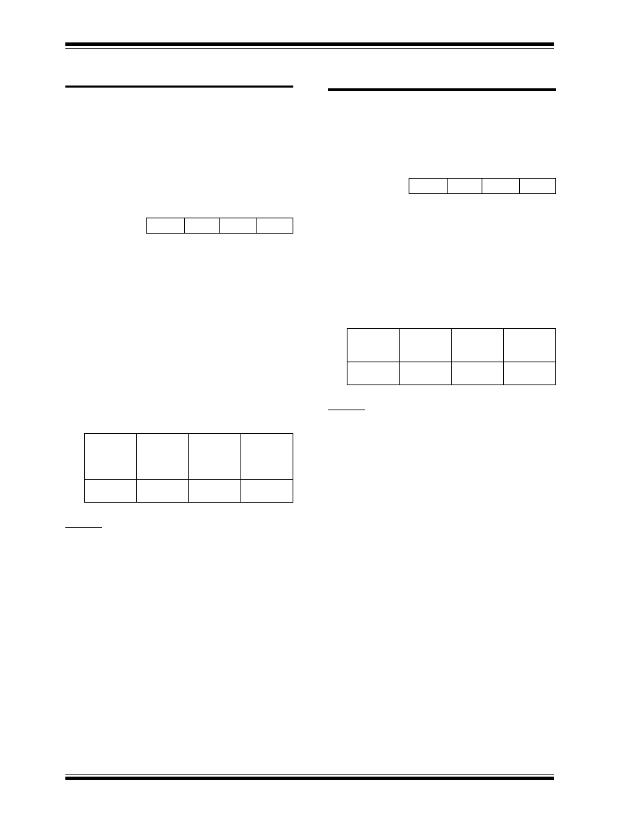
PIC18CXX2
DS39026B-page 222
Preliminary
©
7/99 Microchip Technology Inc.
RETFIE
Return from Interrupt
Syntax:
[
label ] RETFIE s
Operands:
s
[0,1]
Operation:
(TOS)
PC,
1
GIE/GIEH or PEIE/GIEL,
if s = 1
(WS)
WREG,
(STATUSS)
STATUS,
(BSRS)
BSR,
PCLATU, PCLATH are unchanged.
Status Affected:
GIE/GIEH,PEIE/GIEL.
Encoding:
0000
0000
0001
000s
Description:
Return from Interrupt. Stack is
popped and Top of Stack (TOS) is
loaded into the PC. Interrupts are
enabled by setting the either the
high or low priority global inter-
rupt enable bit. If 's' = 1, the con-
tents of the shadow registers WS,
STATUSS and BSRS are loaded
into their corresponding registers,
WREG, STATUS and BSR. If 's' =
0, no update of these registers
occurs (default).
Words:
1
Cycles:
2
Q Cycle Activity:
Q1
Q2
Q3
Q4
Decode
No
operation
No
operation
pop PC from
stack
Set GIEH or
GIEL
No
operation
No
operation
No
operation
No
operation
Example:
RETFIE 1
After Interrupt
PC
=
TOS
W
=
WS
BSR
=
BSRS
STATUS
=
STATUSS
GIE/GIEH, PEIE/GIEL=
1
RETLW
Return Literal to WREG
Syntax:
[
label ] RETLW k
Operands:
0
k
255
Operation:
k
WREG,
(TOS)
PC,
PCLATU, PCLATH are unchanged
Status Affected:
None
Encoding:
0000
1100
kkkk
kkkk
Description:
WREG is loaded with the eight bit
literal 'k'. The program counter is
loaded from the top of the stack
(the return address). The high
address latch (PCLATH) remains
unchanged.
Words:
1
Cycles:
2
Q Cycle Activity:
Q1
Q2
Q3
Q4
Decode
Read
literal 'k'
Process
Data
pop PC from
stack, Write
to WREG
No
operation
No
operation
No
operation
No
operation
Example:
CALL TABLE ; WREG contains table
; offset value
; WREG now has
; table value
:
TABLE
ADDWF PCL ; WREG = offset
RETLW k0 ; Begin table
RETLW k1 ;
:
:
RETLW kn ; End of table
Before Instruction
WREG
=
0x07
After Instruction
WREG
=
value of kn
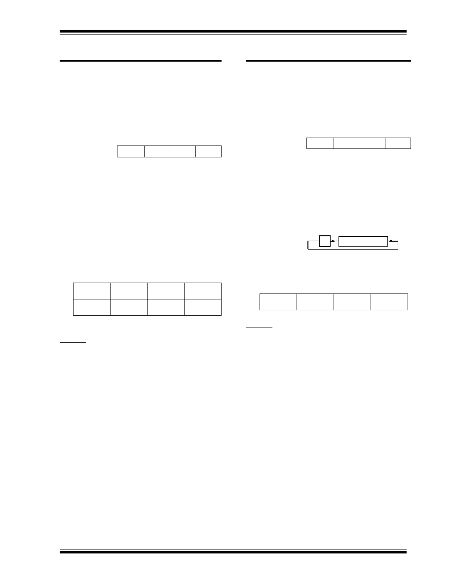
PIC18CXX2
©
7/99 Microchip Technology Inc.
Preliminary
DS39026B-page 223
RETURN
Return from Subroutine
Syntax:
[
label ] RETURN s
Operands:
s
[0,1]
Operation:
(TOS)
PC,
if s = 1
(WS)
WREG,
(STATUSS)
STATUS,
(BSRS)
BSR,
PCLATU, PCLATH are unchanged
Status Affected:
None
Encoding:
0000
0000
0001
001s
Description:
Return from subroutine. The
stack is popped and the top of the
stack (TOS) is loaded into the
program counter. If 's' = 1, the
contents of the shadow registers
WS, STATUSS and BSRS are
loaded into their corresponding
registers, WREG, STATUS and
BSR. If 's' = 0, no update of
these registers occurs (default).
Words:
1
Cycles:
2
Q Cycle Activity:
Q1
Q2
Q3
Q4
Decode
No
operation
Process
Data
pop PC from
stack
No
operation
No
operation
No
operation
No
operation
Example:
RETURN
After Interrupt
PC
= TOS
RLCF
Rotate Left f through Carry
Syntax:
[
label ] RLCF f,d,a
Operands:
0
f
255
d
[0,1]
a
[0,1]
Operation:
(f<n>)
dest<n+1>,
(f<7>)
C,
(C)
dest<0>
Status Affected:
C,N,Z
Encoding:
0011
01da
ffff
ffff
Description:
The contents of register 'f' are
rotated one bit to the left through
the Carry Flag. If 'd' is 0 the result is
placed in WREG. If 'd' is 1 the
result is stored back in register 'f'
(default). If 'a' is 0, the Access
Bank will be selected, overriding
the BSR value. If 'a' = 1, then the
bank will be selected as per the
BSR value (default).
Words:
1
Cycles:
1
Q Cycle Activity:
Q1
Q2
Q3
Q4
Decode
Read
register 'f'
Process
Data
Write to
destination
Example:
RLCF
REG, 0, 0
Before Instruction
REG
=
1110 0110
C
=
0
After Instruction
REG
=
1110 0110
WREG
=
1100 1100
C
=
1
C
register f
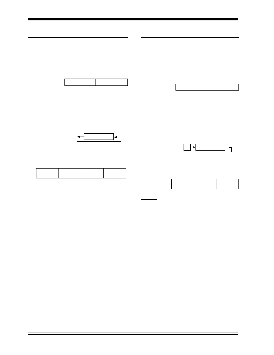
PIC18CXX2
DS39026B-page 224
Preliminary
©
7/99 Microchip Technology Inc.
RLNCF
Rotate Left f (no carry)
Syntax:
[
label ] RLNCF f,d,a
Operands:
0
f
255
d
[0,1]
a
[0,1]
Operation:
(f<n>)
dest<n+1>,
(f<7>)
dest<0>
Status Affected:
N,Z
Encoding:
0100
01da
ffff
ffff
Description:
The contents of register 'f' are
rotated one bit to the left. If 'd' is 0
the result is placed in WREG. If 'd'
is 1, the result is stored back in reg-
ister 'f' (default). If 'a' is 0, the
Access Bank will be selected, over-
riding the BSR value. If 'a' is 1,
then the bank will be selected as
per the BSR value (default).
Words:
1
Cycles:
1
Q Cycle Activity:
Q1
Q2
Q3
Q4
Decode
Read
register 'f'
Process
Data
Write to
destination
Example:
RLNCF
REG, 1, 0
Before Instruction
REG
=
1010 1011
After Instruction
REG
=
0101 0111
register f
RRCF
Rotate Right f through Carry
Syntax:
[
label ] RRCF f,d,a
Operands:
0
f
255
d
[0,1]
a
[0,1]
Operation:
(f<n>)
dest<n-1>,
(f<0>)
C,
(C)
dest<7>
Status Affected:
C,N,Z
Encoding:
0011
00da
ffff
ffff
Description:
The contents of register 'f' are
rotated one bit to the right through
the Carry Flag. If 'd' is 0, the result
is placed in WREG. If 'd' is 1, the
result is placed back in register 'f'
(default). If 'a' is 0, the Access
Bank will be selected, overriding
the BSR value. If 'a' is 1, then the
bank will be selected as per the
BSR value (default).
Words:
1
Cycles:
1
Q Cycle Activity:
Q1
Q2
Q3
Q4
Decode
Read
register 'f'
Process
Data
Write to
destination
Example:
RRCF
REG, 0, 0
Before Instruction
REG
=
1110 0110
C
=
0
After Instruction
REG
=
1110 0110
WREG
=
0111 0011
C
=
0
C
register f
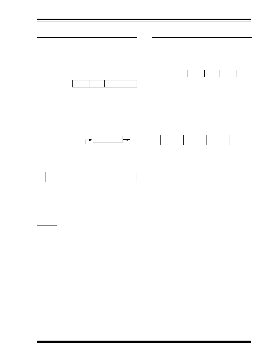
PIC18CXX2
©
7/99 Microchip Technology Inc.
Preliminary
DS39026B-page 225
RRNCF
Rotate Right f (no carry)
Syntax:
[
label ] RRNCF f,d,a
Operands:
0
f
255
d
[0,1]
a
[0,1]
Operation:
(f<n>)
dest<n-1>,
(f<0>)
dest<7>
Status Affected:
N,Z
Encoding:
0100
00da
ffff
ffff
Description:
The contents of register 'f' are
rotated one bit to the right. If 'd' is 0,
the result is placed in WREG. If 'd'
is 1, the result is placed back in
register 'f' (default). If 'a' is 0, the
Access Bank will be selected, over-
riding the BSR value. If 'a' is 1,
then the bank will be selected as
per the BSR value (default).
Words:
1
Cycles:
1
Q Cycle Activity:
Q1
Q2
Q3
Q4
Decode
Read
register 'f'
Process
Data
Write to
destination
Example 1:
RRNCF REG, 1, 0
Before Instruction
REG
=
1101 0111
After Instruction
REG
=
1110 1011
Example 2:
RRNCF REG, 0, 0
Before Instruction
WREG
=
?
REG
=
1101 0111
After Instruction
WREG
=
1110 1011
REG
=
1101 0111
register f
SETF
Set f
Syntax:
[
label] SETF f,a
Operands:
0
f
255
a
[0,1]
Operation:
FFh
f
Status Affected:
None
Encoding:
0110
100a
ffff
ffff
Description:
The contents of the specified regis-
ter are set to FFh. If 'a' is 0, the
Access Bank will be selected, over-
riding the BSR value. If 'a' is 1,
then the bank will be selected as
per the BSR value (default).
Words:
1
Cycles:
1
Q Cycle Activity:
Q1
Q2
Q3
Q4
Decode
Read
register 'f'
Process
Data
Write
register 'f'
Example:
SETF
REG,1
Before Instruction
REG
=
0x5A
After Instruction
REG
=
0xFF
PIC18CXX2
DS39026B-page 226
Preliminary
©
7/99 Microchip Technology Inc.
SLEEP
Enter SLEEP mode
Syntax:
[
label ] SLEEP
Operands:
None
Operation:
00h
WDT,
0
WDT postscaler,
1
TO,
0
PD
Status Affected:
TO, PD
Encoding:
0000
0000
0000
0011
Description:
The power-down status bit (PD) is
cleared. The time-out status bit
(TO) is set. Watchdog Timer and
its postscaler are cleared.
The processor is put into SLEEP
mode with the oscillator stopped.
Words:
1
Cycles:
1
Q Cycle Activity:
Q1
Q2
Q3
Q4
Decode
No
operation
Process
Data
Go to
sleep
Example:
SLEEP
Before Instruction
TO
=
?
PD
=
?
After Instruction
TO
=
1
PD
=
0
If WDT causes wake-up, this bit is cleared
SUBFWB
Subtract f from WREG with
borrow
Syntax:
[
label ] SUBFWB f,d,a
Operands:
0
f
255
d
[0,1]
a
[0,1]
Operation:
(WREG) ≠ (f) ≠ (C)
dest
Status Affected:
N,OV, C, DC, Z
Encoding:
0101
01da
ffff
ffff
Description:
Subtract register 'f' and carry flag
(borrow) from WREG (2's comple-
ment method). If 'd' is 0, the result
is stored in WREG. If 'd' is 1, the
result is stored in register 'f'
(default) . If 'a' is 0, the Access
Bank will be selected, overriding
the BSR value. If 'a' is 1, then the
bank will be selected as per the
BSR value (default).
Words:
1
Cycles:
1
Q Cycle Activity:
Q1
Q2
Q3
Q4
Decode
Read
register 'f'
Process
Data
Write to
destination

PIC18CXX2
©
7/99 Microchip Technology Inc.
Preliminary
DS39026B-page 227
SUBFWB
Example 1:
SUBFWB REG, 1, 0
Before Instruction
REG
=
3
WREG
=
2
C
=
1
After Instruction
REG
=
FF
WREG
=
2
C
=
0
Z
=
0
N
=
1 ; result is negative
Example 2:
SUBFWB REG, 0, 0
Before Instruction
REG
=
2
WREG
=
5
C
=
1
After Instruction
REG
=
2
WREG
=
3
C
=
1
Z
=
0
N
=
0 ; result is positive
Example 3:
SUBFWB REG, 1, 0
Before Instruction
REG
=
1
WREG
=
2
C
=
0
After Instruction
REG
=
0
WREG
=
2
C
=
1
Z
=
1 ; result is zero
N
=
0
SUBLW
Subtract WREG from literal
Syntax:
[
label ] SUBLW k
Operands:
0
k
255
Operation:
k ≠ (WREG)
WREG
Status Affected:
N,OV, C, DC, Z
Encoding:
0000
1000
kkkk
kkkk
Description:
WREG is subtracted from the
eight bit literal 'k'. The result is
placed in WREG.
Words:
1
Cycles:
1
Q Cycle Activity:
Q1
Q2
Q3
Q4
Decode
Read
literal 'k'
Process
Data
Write to
WREG
Example 1:
SUBLW
0x02
Before Instruction
WREG
=
1
C
=
?
After Instruction
WREG
=
1
C
=
1 ; result is positive
Z
=
0
N
=
0
Example 2:
SUBLW
0x02
Before Instruction
WREG
=
2
C
=
?
After Instruction
WREG
=
0
C
=
1 ; result is zero
Z
=
1
N
=
0
Example 3:
SUBLW
0x02
Before Instruction
WREG
=
3
C
=
?
After Instruction
WREG
=
FF ; (2's complement)
C
=
0 ; result is negative
Z
=
0
N
=
1
PIC18CXX2
DS39026B-page 228
Preliminary
©
7/99 Microchip Technology Inc.
SUBWF
Subtract WREG from f
Syntax:
[
label ] SUBWF f,d,a
Operands:
0
f
255
d
[0,1]
a
[0,1]
Operation:
(f) ≠ (WREG)
dest
Status Affected:
N,OV, C, DC, Z
Encoding:
0101
11da
ffff
ffff
Description:
Subtract WREG from register 'f'
(2's complement method). If 'd' is
0, the result is stored in WREG. If
'd' is 1, the result is stored back in
register 'f' (default). If 'a' is 0, the
Access Bank will be selected,
overriding the BSR value. If 'a' is
1, then the bank will be selected
as per the BSR value (default).
Words:
1
Cycles:
1
Q Cycle Activity:
Q1
Q2
Q3
Q4
Decode
Read
register 'f'
Process
Data
Write to
destination
SUBWF
Subtract WREG from f (cont'd)
Example 1:
SUBWF REG, 1, 0
Before Instruction
REG
=
3
WREG
=
2
C
=
?
After Instruction
REG
=
1
WREG
=
2
C
=
1 ; result is positive
Z
=
0
N
=
0
Example 2:
SUBWF REG, 0, 0
Before Instruction
REG
=
2
WREG
=
2
C
=
?
After Instruction
REG
=
2
WREG
=
0
C
=
1 ; result is zero
Z
=
1
N
=
0
Example 3:
SUBWF REG, 1, 0
Before Instruction
REG
=
1
WREG
=
2
C
=
?
After Instruction
REG
=
FFh ;(2's complement)
WREG
=
2
C
=
0 ; result is negative
Z
=
0
N
=
1
PIC18CXX2
©
7/99 Microchip Technology Inc.
Preliminary
DS39026B-page 229
SUBWFB
Subtract WREG from f with
Borrow
Syntax:
[
label ] SUBWFB f,d,a
Operands:
0
f
255
d
[0,1]
a
[0,1]
Operation:
(f) ≠ (WREG) ≠ (C)
dest
Status Affected:
N,OV, C, DC, Z
Encoding:
0101
10da
ffff
ffff
Description:
Subtract WREG and the carry flag
(borrow) from register 'f' (2's com-
plement method). If 'd' is 0, the
result is stored in WREG. If 'd' is
1, the result is stored back in reg-
ister 'f' (default). If 'a' is 0, the
Access Bank will be selected,
overriding the BSR value. If 'a' is
1, then the bank will be selected
as per the BSR value (default).
Words:
1
Cycles:
1
Q Cycle Activity:
Q1
Q2
Q3
Q4
Decode
Read
register 'f'
Process
Data
Write to
destination
SUBWFB
Subtract WREG from f with
Borrow (cont'd)
Example 1:
SUBWFB REG, 1, 0
Before Instruction
REG
=
0x19 (0001 1001)
WREG
=
0x0D (0000 1101)
C
=
1
After Instruction
REG
=
0x0C (0000 1011)
WREG
=
0x0D (0000 1101)
C
=
1
Z
=
0
N
=
0
; result is positive
Example2:
SUBWFBREG, 0, 0
Before Instruction
REG
=
0x1B (0001 1011)
WREG
=
0x1A (0001 1010)
C
=
0
After Instruction
REG
=
0x1B
(0001 1011)
WREG
=
0x00
C
=
1
Z
=
1 ; result is zero
N
=
0
Example3:
SUBWFBREG, 1, 0
Before Instruction
REG
=
0x03 (0000 0011)
WREG
=
0x0E
(0000 1101)
C
=
1
After Instruction
REG
=
0xF5
(1111 0100) [2's
comp]
WREG
=
0x0E
(0000 1101)
C
=
0
Z
=
0
N
=
1 ; result is negative
PIC18CXX2
DS39026B-page 230
Preliminary
©
7/99 Microchip Technology Inc.
SWAPF
Swap f
Syntax:
[
label ] SWAPF f,d,a
Operands:
0
f
255
d
[0,1]
a
[0,1]
Operation:
(f<3:0>)
dest<7:4>,
(f<7:4>)
dest<3:0>
Status Affected:
None
Encoding:
0011
10da
ffff
ffff
Description:
The upper and lower nibbles of reg-
ister 'f' are exchanged. If 'd' is 0, the
result is placed in WREG. If 'd' is 1,
the result is placed in register 'f'
(default). If 'a' is 0, the Access
Bank will be selected, overriding
the BSR value. If 'a' is 1, then the
bank will be selected as per the
BSR value (default).
Words:
1
Cycles:
1
Q Cycle Activity:
Q1
Q2
Q3
Q4
Decode
Read
register 'f'
Process
Data
Write to
destination
Example:
SWAPF
REG, 1, 0
Before Instruction
REG
=
0x53
After Instruction
REG
=
0x35
PIC18CXX2
©
7/99 Microchip Technology Inc.
Preliminary
DS39026B-page 231
TBLRD
Table Read
Syntax:
[
label ]
TBLRD ( *; *+; *-; +*)
Operands:
None
Operation: if
TBLRD
*,
(Prog Mem (TBLPTR))
TABLAT;
TBLPTR - No Change;
if TBLRD *+,
(Prog Mem (TBLPTR))
TABLAT;
(TBLPTR) +1
TBLPTR;
if TBLRD *-,
(Prog Mem (TBLPTR))
TABLAT;
(TBLPTR) -1
TBLPTR;
if TBLRD +*,
(TBLPTR) +1
TBLPTR;
(Prog Mem (TBLPTR))
TABLAT;
Status Affected:
None
Encoding:
0000
0000
0000
10nn
nn=0 *
=1 *+
=2 *-
=3 +*
Description:
This instruction is used to read the
contents of Program Memory (P.M.). To
address the program memory a pointer
called Table Pointer (TBLPTR) is used.
The TBLPTR (a 21-bit pointer) points
to each byte in the program memory.
TBLPTR has a 2 Mbyte address range.
TBLPTR[0] = 0:Least
Significant
Byte of Program
Memory Word
TBLPTR[0] = 1:Most
Significant
Byte of Program
Memory Word
The TBLRD instruction can modify the
value of TBLPTR as follows:
∑ no change
∑ post-increment
∑ post-decrement
∑ pre-increment
Words:
1
Cycles:
2
Q Cycle Activity:
Q1
Q2
Q3
Q4
Decode
No
operation
No
operation
No
operation
No
operation
No
operation
(Read
Program
Memory)
No
operation
No
operation
(Write
TABLAT)
TBLRD
Table Read (cont'd)
Example1:
TBLRD *+ ;
Before Instruction
TABLAT
=
0x55
TBLPTR
=
0x00A356
MEMORY(0x00A356)
=
0x34
After Instruction
TABLAT
=
0x34
TBLPTR
=
0x00A357
Example2:
TBLRD +* ;
Before Instruction
TABLAT
=
0xAA
TBLPTR
=
0x01A357
MEMORY(0x01A357)
=
0x12
MEMORY(0x01A358)
=
0x34
After Instruction
TABLAT
=
0x34
TBLPTR
=
0x01A358
PIC18CXX2
DS39026B-page 232
Preliminary
©
7/99 Microchip Technology Inc.
TBLWT Table
Write
Syntax:
[
label
]
TBLWT ( *; *+; *-; +*)
Operands:
None
Operation:
if TBLWT*,
(TABLAT)
Prog Mem (TBLPTR) or
Holding Register;
TBLPTR - No Change;
if TBLWT*+,
(TABLAT)
Prog Mem (TBLPTR) or
Holding Register;
(TBLPTR) +1
TBLPTR;
if TBLWT*-,
(TABLAT)
Prog Mem (TBLPTR) or
Holding Register;
(TBLPTR) -1
TBLPTR;
if TBLWT+*,
(TBLPTR) +1
TBLPTR;
(TABLAT)
Prog Mem (TBLPTR) or
Holding Register;
Status Affected:
None
Encoding:
0000
0000
0000
11nn
nn=0 *
=1 *+
=2 *-
=3 +*
Description:
This instruction is used to program the
contents of Program Memory (P.M.).
The TBLPTR (a 21-bit pointer) points
to each byte in the program memory.
TBLPTR has a 2 MBtye address
range. The LSb of the TBLPTR
selects which byte of the program
memory location to access.
TBLPTR[0] = 0:Least Significant
Byte of Program
Memory Word
TBLPTR[0] = 1:Most Significant
Byte of Program
Memory Word
The TBLWT instruction can modify the
value of TBLPTR as follows:
∑ no change
∑ post-increment
∑ post-decrement
∑ pre-increment
Words:
1
Cycles:
2 (many if long write is to on-chip
EPROM program memory)
Q Cycle Activity:
Q1
Q2
Q3
Q4
Decode
No
operation
No
operation
No
operation
No
operation
No
operation
(Read
TABLAT)
No
operation
No
operation
(Write to Holding
Register or Memory)
TBLWT
Table Write (cont.'d)
Example1:
TBLWT *+;
Before Instruction
TABLAT =
0x55
TBLPTR
=
0x00A356
MEMORY(0x00A356)
=
0xFF
After Instructions (table write completion)
TABLAT
=
0x55
TBLPTR
=
0x00A357
MEMORY(0x00A356)
=
0x55
Example 2:
TBLWT +*;
Before Instruction
TABLAT
=
0x34
TBLPTR
=
0x01389A
MEMORY(0x01389A)
=
0xFF
MEMORY(0x01389B)
=
0xFF
After Instruction (table write completion)
TABLAT
=
0x34
TBLPTR
=
0x01389B
MEMORY(0x01389A)
=
0xFF
MEMORY(0x01389B)
=
0x34
PIC18CXX2
©
7/99 Microchip Technology Inc.
Preliminary
DS39026B-page 233
TSTFSZ
Test f, skip if 0
Syntax:
[
label ] TSTFSZ f,a
Operands:
0
f
255
a
[0,1]
Operation:
skip if f = 0
Status Affected:
None
Encoding:
0110
011a
ffff
ffff
Description:
If 'f' = 0, the next instruction,
fetched during the current instruc-
tion execution, is discarded and a
NOP
is executed making this a two-
cycle instruction. If 'a' is 0, the
Access Bank will be selected, over-
riding the BSR value. If 'a' is 1,
then the bank will be selected as
per the BSR value (default).
Words:
1
Cycles:
1(2)
Note: 3 cycles if skip and followed
by a 2-word instruction
Q Cycle Activity:
Q1
Q2
Q3
Q4
Decode
Read
register 'f'
Process
Data
No
operation
If skip:
Q1
Q2
Q3
Q4
No
operation
No
operation
No
operation
No
operation
If skip and followed by 2-word instruction:
Q1
Q2
Q3
Q4
No
operation
No
operation
No
operation
No
operation
No
operation
No
operation
No
operation
No
operation
Example:
HERE TSTFSZ CNT, 1
NZERO :
ZERO :
Before Instruction
PC = Address(HERE)
After Instruction
If CNT
=
0x00,
PC =
Address
(ZERO)
If CNT
0x00,
PC =
Address
(NZERO)
XORLW
Exclusive OR literal with WREG
Syntax:
[
label ] XORLW k
Operands:
0
k
255
Operation:
(WREG) .XOR. k
WREG
Status Affected:
N,Z
Encoding:
0000
1010
kkkk
kkkk
Description:
The contents of WREG are
XOR'ed with the 8-bit literal 'k'.
The result is placed in WREG.
Words:
1
Cycles:
1
Q Cycle Activity:
Q1
Q2
Q3
Q4
Decode
Read
literal 'k'
Process
Data
Write to
WREG
Example:
XORLW 0xAF
Before Instruction
WREG
=
0xB5
After Instruction
WREG
=
0x1A
PIC18CXX2
DS39026B-page 234
Preliminary
©
7/99 Microchip Technology Inc.
XORWF
Exclusive OR WREG with f
Syntax:
[
label ] XORWF f,d,a
Operands:
0
f
255
d
[0,1]
a
[0,1]
Operation:
(WREG) .XOR. (f)
dest
Status Affected:
N,Z
Encoding:
0001
10da
ffff
ffff
Description:
Exclusive OR the contents of
WREG with register 'f'. If 'd' is 0, the
result is stored in WREG. If 'd' is 1,
the result is stored back in the reg-
ister 'f' (default). If 'a' is 0, the
Access Bank will be selected, over-
riding the BSR value. If 'a' is 1,
then the bank will be selected as
per the BSR value (default).
Words:
1
Cycles:
1
Q Cycle Activity:
Q1
Q2
Q3
Q4
Decode
Read
register 'f'
Process
Data
Write to
destination
Example:
XORWF REG, 1, 0
Before Instruction
REG
=
0xAF
WREG
=
0xB5
After Instruction
REG
=
0x1A
WREG
=
0xB5

©
1999 Microchip Technology Inc.
Preliminary
DS39026B-page 235
PIC18CXX2
20.0
DEVELOPMENT SUPPORT
The PICmicro
Æ
microcontrollers are supported with a
full range of hardware and software development tools:
∑ Integrated Development Environment
- MPLABTM IDE Software
∑ Assemblers/Compilers/Linkers
- MPASM Assembler
- MPLAB-C17 and MPLAB-C18 C Compilers
- MPLINK/MPLIB Linker/Librarian
∑ Simulators
- MPLAB-SIM Software Simulator
∑ Emulators
- MPLAB-ICE
Real-Time In-Circuit Emulator
- PICMASTER
Æ
/PICMASTER-CE In-Circuit
Emulator
- ICEPICTM
∑ In-Circuit Debugger
- MPLAB-ICD for PIC16F877
∑ Device Programmers
- PRO MATE
Æ
II Universal Programmer
- PICSTART
Æ
Plus Entry-Level Prototype
Programmer
∑ Low-Cost Demonstration Boards
- SIMICE
- PICDEM-1
- PICDEM-2
- PICDEM-3
- PICDEM-17
- SEEVAL
Æ
- K
EE
L
OQ
Æ
20.1
MPLAB Integrated Development
Environment Software
- The MPLAB IDE software brings an ease of
software development previously unseen in
the 8-bit microcontroller market. MPLAB is a
Windows
Æ
-based application which contains:
∑ Multiple functionality
- editor
- simulator
- programmer (sold separately)
- emulator (sold separately)
∑ A full featured editor
∑ A project manager
∑ Customizable tool bar and key mapping
∑ A status bar
∑ On-line help
MPLAB allows you to:
∑ Edit your source files (either assembly or `C')
∑ One touch assemble (or compile) and download
to PICmicro tools (automatically updates all
project information)
∑ Debug using:
- source files
- absolute listing file
- object code
The ability to use MPLAB with Microchip's simulator,
MPLAB-SIM, allows a consistent platform and the abil-
ity to easily switch from the cost-effective simulator to
the full featured emulator with minimal retraining.
20.2
MPASM Assembler
MPASM is a full featured universal macro assembler for
all PICmicro MCU's. It can produce absolute code
directly in the form of HEX files for device program-
mers, or it can generate relocatable objects for
MPLINK.
MPASM has a command line interface and a Windows
shell and can be used as a standalone application on a
Windows 3.x or greater system. MPASM generates
relocatable object files, Intel standard HEX files, MAP
files to detail memory usage and symbol reference, an
absolute LST file which contains source lines and gen-
erated machine code, and a COD file for MPLAB
debugging.
MPASM features include:
∑ MPASM and MPLINK are integrated into MPLAB
projects.
∑ MPASM allows user defined macros to be created
for streamlined assembly.
∑ MPASM allows conditional assembly for multi pur-
pose source files.
∑ MPASM directives allow complete control over the
assembly process.
20.3
MPLAB-C17 and MPLAB-C18
C Compilers
The MPLAB-C17 and MPLAB-C18 Code Development
Systems are complete ANSI `C' compilers and inte-
grated development environments for Microchip's
PIC17CXXX and PIC18CXXX family of microcontrol-
lers, respectively. These compilers provide powerful
integration capabilities and ease of use not found with
other compilers.
For easier source level debugging, the compilers pro-
vide symbol information that is compatible with the
MPLAB IDE memory display.

PIC18CXX2
DS39026B-page 236
Preliminary
©
1999 Microchip Technology Inc.
20.4
MPLINK/MPLIB Linker/Librarian
MPLINK is a relocatable linker for MPASM and
MPLAB-C17 and MPLAB-C18. It can link relocatable
objects from assembly or C source files along with pre-
compiled libraries using directives from a linker script.
MPLIB is a librarian for pre-compiled code to be used
with MPLINK. When a routine from a library is called
from another source file, only the modules that contains
that routine will be linked in with the application. This
allows large libraries to be used efficiently in many dif-
ferent applications. MPLIB manages the creation and
modification of library files.
MPLINK features include:
∑ MPLINK works with MPASM and MPLAB-C17
and MPLAB-C18.
∑ MPLINK allows all memory areas to be defined as
sections to provide link-time flexibility.
MPLIB features include:
∑ MPLIB makes linking easier because single librar-
ies can be included instead of many smaller files.
∑ MPLIB helps keep code maintainable by grouping
related modules together.
∑ MPLIB commands allow libraries to be created
and modules to be added, listed, replaced,
deleted, or extracted.
20.5
MPLAB-SIM Software Simulator
The MPLAB-SIM Software Simulator allows code
development in a PC host environment by simulating
the PICmicro series microcontrollers on an instruction
level. On any given instruction, the data areas can be
examined or modified and stimuli can be applied from
a file or user-defined key press to any of the pins. The
execution can be performed in single step, execute until
break, or trace mode.
MPLAB-SIM fully supports symbolic debugging using
MPLAB-C17 and MPLAB-C18 and MPASM. The Soft-
ware Simulator offers the flexibility to develop and
debug code outside of the laboratory environment mak-
ing it an excellent multi-project software development
tool.
20.6
MPLAB-ICE High Performance
Universal In-Circuit Emulator with
MPLAB IDE
The MPLAB-ICE Universal In-Circuit Emulator is
intended to provide the product development engineer
with a complete microcontroller design tool set for
PICmicro microcontrollers (MCUs). Software control of
MPLAB-ICE is provided by the MPLAB Integrated
Development Environment (IDE), which allows editing,
"make" and download, and source debugging from a
single environment.
Interchangeable processor modules allow the system
to be easily reconfigured for emulation of different pro-
cessors. The universal architecture of the MPLAB-ICE
allows expansion to support new PICmicro microcon-
trollers.
The MPLAB-ICE Emulator System has been designed
as a real-time emulation system with advanced fea-
tures that are generally found on more expensive devel-
opment tools. The PC platform and Microsoft
Æ
Windows
3.x/95/98 environment were chosen to best make these
features available to you, the end user.
MPLAB-ICE 2000 is a full-featured emulator system
with enhanced trace, trigger, and data monitoring fea-
tures. Both systems use the same processor modules
and will operate across the full operating speed range
of the PICmicro MCU.
20.7
PICMASTER/PICMASTER CE
The PICMASTER system from Microchip Technology is
a full-featured, professional quality emulator system.
This flexible in-circuit emulator provides a high-quality,
universal platform for emulating Microchip 8-bit
PICmicro microcontrollers (MCUs). PICMASTER sys-
tems are sold worldwide, with a CE compliant model
available for European Union (EU) countries.
20.8
ICEPIC
ICEPIC is a low-cost in-circuit emulation solution for the
Microchip Technology PIC16C5X, PIC16C6X,
PIC16C7X, and PIC16CXXX families of 8-bit one-time-
programmable (OTP) microcontrollers. The modular
system can support different subsets of PIC16C5X or
PIC16CXXX products through the use of
interchangeable personality modules or daughter
boards. The emulator is capable of emulating without
target application circuitry being present.
20.9
MPLAB-ICD In-Circuit Debugger
Microchip's In-Circuit Debugger, MPLAB-ICD, is a pow-
erful, low-cost run-time development tool. This tool is
based on the flash PIC16F877 and can be used to
develop for this and other PICmicro microcontrollers
from the PIC16CXXX family. MPLAB-ICD utilizes the
In-Circuit Debugging capability built into the
PIC16F87X. This feature, along with Microchip's In-Cir-
cuit Serial Programming protocol, offers cost-effective
in-circuit flash programming and debugging from the
graphical user interface of the MPLAB Integrated
Development Environment. This enables a designer to
develop and debug source code by watching variables,
single-stepping and setting break points. Running at
full speed enables testing hardware in real-time. The
MPLAB-ICD is also a programmer for the flash
PIC16F87X family.

©
1999 Microchip Technology Inc.
Preliminary
DS39026B-page 237
PIC18CXX2
20.10
PRO MATE II Universal Programmer
The PRO MATE II Universal Programmer is a full-fea-
tured programmer capable of operating in stand-alone
mode as well as PC-hosted mode. PRO MATE II is CE
compliant.
The PRO MATE II has programmable V
DD
and V
PP
supplies which allows it to verify programmed memory
at V
DD
min and V
DD
max for maximum reliability. It has
an LCD display for instructions and error messages,
keys to enter commands and a modular detachable
socket assembly to support various package types. In
stand-alone mode the PRO MATE II can read, verify or
program PICmicro devices. It can also set code-protect
bits in this mode.
20.11
PICSTART Plus Entry Level
Development System
The PICSTART programmer is an easy-to-use, low-
cost prototype programmer. It connects to the PC via
one of the COM (RS-232) ports. MPLAB Integrated
Development Environment software makes using the
programmer simple and efficient.
PICSTART Plus supports all PICmicro devices with up
to 40 pins. Larger pin count devices such as the
PIC16C92X, and PIC17C76X may be supported with
an adapter socket. PICSTART Plus is CE compliant.
20.12
SIMICE Entry-Level
Hardware Simulator
SIMICE is an entry-level hardware development sys-
tem designed to operate in a PC-based environment
with Microchip's simulator MPLAB-SIM. Both SIMICE
and MPLAB-SIM run under Microchip Technology's
MPLAB Integrated Development Environment (IDE)
software. Specifically, SIMICE provides hardware sim-
ulation for Microchip's PIC12C5XX, PIC12CE5XX, and
PIC16C5X families of PICmicro 8-bit microcontrollers.
SIMICE works in conjunction with MPLAB-SIM to pro-
vide non-real-time I/O port emulation. SIMICE enables
a developer to run simulator code for driving the target
system. In addition, the target system can provide input
to the simulator code. This capability allows for simple
and interactive debugging without having to manually
generate MPLAB-SIM stimulus files. SIMICE is a valu-
able debugging tool for entry-level system develop-
ment.
20.13
PICDEM-1 Low-Cost PICmicro
Demonstration Board
The PICDEM-1 is a simple board which demonstrates
the capabilities of several of Microchip's microcontrol-
lers. The microcontrollers supported are: PIC16C5X
(PIC16C54 to PIC16C58A), PIC16C61, PIC16C62X,
PIC16C71, PIC16C8X, PIC17C42, PIC17C43 and
PIC17C44. All necessary hardware and software is
included to run basic demo programs. The users can
program the sample microcontrollers provided with
the PICDEM-1 board, on a PRO MATE II or
PICSTART-Plus programmer, and easily test firm-
ware. The user can also connect the PICDEM-1
board to the MPLAB-ICE emulator and download the
firmware to the emulator for testing. Additional proto-
type area is available for the user to build some addi-
tional hardware and connect it to the microcontroller
socket(s). Some of the features include an RS-232
interface, a potentiometer for simulated analog input,
push-button switches and eight LEDs connected to
PORTB.
20.14
PICDEM-2 Low-Cost PIC16CXX
Demonstration Board
The PICDEM-2 is a simple demonstration board that
supports the PIC16C62, PIC16C64, PIC16C65,
PIC16C73 and PIC16C74 microcontrollers. All the
necessary hardware and software is included to
run the basic demonstration programs. The user
can program the sample microcontrollers provided
with the PICDEM-2 board, on a PRO MATE II pro-
grammer or PICSTART-Plus, and easily test firmware.
The MPLAB-ICE emulator may also be used with the
PICDEM-2 board to test firmware. Additional prototype
area has been provided to the user for adding addi-
tional hardware and connecting it to the microcontroller
socket(s). Some of the features include a RS-232 inter-
face, push-button switches, a potentiometer for simu-
lated analog input, a Serial EEPROM to demonstrate
usage of the I
2
C bus and separate headers for connec-
tion to an LCD module and a keypad.
20.15
PICDEM-3 Low-Cost PIC16CXXX
Demonstration Board
The PICDEM-3 is a simple demonstration board that
supports the PIC16C923 and PIC16C924 in the PLCC
package. It will also support future 44-pin PLCC
microcontrollers with a LCD Module. All the neces-
sary hardware and software is included to run the
basic demonstration programs. The user can pro-
gram the sample microcontrollers provided with
the PICDEM-3 board, on a PRO MATE II program-
mer or PICSTART Plus with an adapter socket, and
easily test firmware. The MPLAB-ICE emulator may
also be used with the PICDEM-3 board to test firm-
ware. Additional prototype area has been provided to
the user for adding hardware and connecting it to the
microcontroller socket(s). Some of the features include
an RS-232 interface, push-button switches, a potenti-
ometer for simulated analog input, a thermistor and
separate headers for connection to an external LCD
module and a keypad. Also provided on the PICDEM-3
board is an LCD panel, with 4 commons and 12 seg-
ments, that is capable of displaying time, temperature
and day of the week. The PICDEM-3 provides an addi-
tional RS-232 interface and Windows 3.1 software for
showing the demultiplexed LCD signals on a PC. A sim-
ple serial interface allows the user to construct a hard-
ware demultiplexer for the LCD signals.

PIC18CXX2
DS39026B-page 238
Preliminary
©
1999 Microchip Technology Inc.
20.16
PICDEM-17
The PICDEM-17 is an evaluation board that demon-
strates the capabilities of several Microchip microcon-
trollers, including PIC17C752, PIC17C756,
PIC17C762, and PIC17C766. All necessary hardware
is included to run basic demo programs, which are sup-
plied on a 3.5-inch disk. A programmed sample is
included, and the user may erase it and program it with
the other sample programs using the PRO MATE II or
PICSTART Plus device programmers and easily debug
and test the sample code. In addition, PICDEM-17 sup-
ports down-loading of programs to and executing out of
external FLASH memory on board. The PICDEM-17 is
also usable with the MPLAB-ICE or PICMASTER emu-
lator, and all of the sample programs can be run and
modified using either emulator. Additionally, a gener-
ous prototype area is available for user hardware.
20.17
SEEVAL Evaluation and Programming
System
The SEEVAL SEEPROM Designer's Kit supports all
Microchip 2-wire and 3-wire Serial EEPROMs. The kit
includes everything necessary to read, write, erase or
program special features of any Microchip SEEPROM
product including Smart Serials
TM
and secure serials.
The Total Endurance
TM
Disk is included to aid in trade-
off analysis and reliability calculations. The total kit can
significantly reduce time-to-market and result in an
optimized system.
20.18
K
EE
L
OQ
Evaluation and
Programming Tools
K
EE
L
OQ
evaluation and programming tools support
Microchips HCS Secure Data Products. The HCS eval-
uation kit includes an LCD display to show changing
codes, a decoder to decode transmissions, and a pro-
gramming interface to program test transmitters.

©
1999 Microchip Technology Inc.
Preliminary
DS39026B-page 239
PIC18CXX2
TABLE 20-1:
DEVELOPMENT TOOLS FROM MICROCHIP
PIC
12
CXXX
PIC
1400
0
PIC
16C
5X
PIC
16C
6X
PIC
16
CXXX
PIC
16F
62X
PIC
16C
7X
PIC1
6C
7X
X
PIC
16C
8X
PIC
16F
8XX
PIC1
6C
9X
X
PIC
17C
4X
PIC1
7C
7X
X
PIC1
8C
XX
2
24
CXX/
25
CXX/
93C
XX
HCSXXX
MCRF
XX
X
MC
P251
0
So
ftw
are
Tool
s
MP
L
A
B
TM
In
te
gr
at
ed
D
eve
lo
pm
en
t E
n
vi
r
o
nm
e
n
t
·
·
·
·
·
·
·
·
·
·
·
·
·
·
MP
L
A
B
TM
C
1
7
C
o
mpi
l
e
r
·
·
MP
L
A
B
TM
C
18 C
o
m
p
iler
·
MP
A
S
M/
MP
L
I
N
K
·
·
·
·
·
·
·
·
·
·
·
·
·
·
·
·
Emula
tor
s
MP
L
A
B
TM-
I
C
E
·
·
·
·
·
·
**
·
·
·
·
·
·
·
·
P
I
CM
AST
E
R/PICM
AST
E
R-
CE
·
·
·
·
·
·
·
·
·
·
·
I
C
EPI
C
TM
Lo
w
-
C
o
s
t
In
-
C
ir
cu
it E
m
u
l
at
o
r
·
·
·
·
·
·
·
·
De
bugge
r
M
P
L
AB-
ICD
In
-
C
ir
c
u
it
De
b
u
g
g
e
r
·
*
·
*
·
Pro
gra
mmers
P
I
CST
ART
Æ
Pl
us
L
o
w-
Co
s
t
Un
ive
r
s
a
l
Dev.
Kit
·
·
·
·
·
·
**
·
·
·
·
·
·
·
·
PR
O
M
A
TE
Æ
II
U
n
iv
er
sa
l P
r
og
r
a
m
m
e
r
·
·
·
·
·
·
**
·
·
·
·
·
·
·
·
·
·
De
mo B
oa
rds
and Ev
al K
its
SI
M
I
C
E
·
·
P
I
CDEM
-
1
·
·
·
·
·
P
I
CDEM
-
2
·
·
·
P
I
CDEM
-
3
·
P
I
CDEM
-
1
4
A
·
P
I
CDEM
-
1
7
·
K
EE
L
OQ
Æ
Ev
a
l
ua
t
i
o
n
Ki
t
·
K
EE
L
OQ
Tr
an
sp
on
de
r K
i
t
·
mi
c
r
oI
D
TM P
r
ogr
am
m
e
r
'
s K
i
t
·
125
k
H
z m
i
c
r
o
I
D
D
eve
lo
pe
r
'
s
K
i
t
·
125
kHz
An
t
i
co
llis
io
n
m
i
c
r
o
I
D
D
eve
lo
pe
r
'
s
K
i
t
·
13.
56 M
H
z A
n
t
i
co
lli
sio
n
m
i
cr
o
I
D
D
eve
lo
pe
r
'
s
K
i
t
·
M
C
P2
5
1
0
CAN De
v
e
l
o
p
e
r
'
s
K
i
t
·
*
C
o
n
ta
ct th
e M
i
cro
c
hip
T
e
chn
o
log
y
In
c. web
site a
t
www
.m
icroc
h
ip
.c
om
f
o
r
inf
o
r
m
a
t
ion
on
how to
use
the
M
P
L
A
B
-
ICD I
n
-Cir
cuit D
e
b
u
gge
r (
D
V
1
64
001
) w
i
t
h
P
I
C
1
6C
62
, 63
, 6
4
, 6
5
,
72,
73,
74
, 76
, 77
*
*
Co
n
t
a
c
t M
i
cr
o
c
h
i
p
T
e
c
h
n
o
lo
g
y
In
c. f
o
r
a
v
a
ila
b
ility
d
a
t
e
.
De
ve
lo
p
m
e
n
t
to
o
l
is a
v
a
ila
b
l
e
o
n
se
le
ct d
e
vice
s
.

PIC18CXX2
DS39026B-page 240
Preliminary
©
1999 Microchip Technology Inc.
NOTES:

PIC18CXX2
©
7/99 Microchip Technology Inc.
Preliminary
DS39026B-page 241
21.0
ELECTRICAL CHARACTERISTICS
Absolute Maximum Ratings
()
Ambient temperature under bias............................................................................................................ .-55∞C to +125∞C
Storage temperature .............................................................................................................................. -65∞C to +150∞C
Voltage on any pin with respect to V
SS
(except V
DD
, MCLR, and RA4).......................................... -0.3V to (V
DD
+ 0.3V)
Voltage on V
DD
with respect to V
SS
......................................................................................................... -0.3V to +7.5V
Voltage on MCLR with respect to V
SS
(Note 2).......................................................................................... 0V to +13.25V
Voltage on RA4 with respect to Vss ............................................................................................................... 0V to +8.5V
Total power dissipation (Note 1) ................................................................................................................................ 1.0W
Maximum current out of V
SS
pin ........................................................................................................................... 300 mA
Maximum current into V
DD
pin .............................................................................................................................. 250 mA
Input clamp current, I
IK
(V
I
< 0 or V
I
> V
DD
)
...................................................................................................................... ±
20 mA
Output clamp current, I
OK
(V
O
< 0 or V
O
> V
DD
)
.............................................................................................................. ±
20 mA
Maximum output current sunk by any I/O pin..........................................................................................................25 mA
Maximum output current sourced by any I/O pin .................................................................................................... 25 mA
Maximum current sunk by
PORTA, PORTB, and PORTE (Note 3) (combined).................................................... 200 mA
Maximum current sourced by PORTA, PORTB, and PORTE (Note 3) (combined) .............................................. 200 mA
Maximum current sunk by PORTC and PORTD
(Note 3) (combined) .................................................................. 200 mA
Maximum current sourced by PORTC and PORTD
(Note 3)
(combined) ............................................................. 200 mA
Note 1: Power dissipation is calculated as follows:
Pdis = V
DD
x {I
DD
-
I
OH
} +
{(V
DD
-V
OH
) x I
OH
} +
(V
O
l x I
OL
)
Note 2: Voltage spikes below V
SS
at the MCLR/V
PP
pin, inducing currents greater than 80 mA, may cause latch-up.
Thus, a series resistor of 50-100
should be used when applying a "low" level to the MCLR/V
PP
pin, rather
than pulling this pin directly to V
SS
.
Note 3: PORTD and PORTE not available on the PIC18C2X2 devices.
NOTICE: Stresses above those listed under "Absolute Maximum Ratings" may cause permanent damage to the
device. This is a stress rating only and functional operation of the device at those or any other conditions above those
indicated in the operation listings of this specification is not implied. Exposure to maximum rating conditions for
extended periods may affect device reliability.
PIC18CXX2
DS39026B-page 242
Preliminary
©
7/99 Microchip Technology Inc.
FIGURE 21-1: PIC18CXX2 VOLTAGE-FREQUENCY GRAPH (INDUSTRIAL)
FIGURE 21-2: PIC18LCXX2 VOLTAGE-FREQUENCY GRAPH (INDUSTRIAL)
Frequency
Vo
l
t
a
g
e
6.0 V
5.5 V
4.5 V
4.0 V
2.0 V
40 MHz
5.0 V
3.5 V
3.0 V
2.5 V
PIC18CXXX
4.2V
Frequency
Vo
l
t
a
g
e
6.0 V
5.5 V
4.5 V
4.0 V
2.0 V
40 MHz
5.0 V
3.5 V
3.0 V
2.5 V
PIC18LCXXX
F
MAX
= (20.0 MHz/V) (V
DDAPPMIN
- 2.5 V) + 6 MHz
Note: V
DDAPPMIN
is the minimum voltage of the PICmicro
Æ
device in the application
6 MHz
4.2V
PIC18CXX2
©
7/99 Microchip Technology Inc.
Preliminary
DS39026B-page 243
21.1
DC Characteristics: PIC18CXX2 (Industrial, Extended)
DC CHARACTERISTICS
Standard Operating Conditions (unless otherwise stated)
Operating temperature
-40∞C
T
A
+85∞C for industrial
-40∞C
T
A
+125∞C for extended
Param
No.
Symbol
Characteristic
Min
Typ
Max Units
Conditions
V
DD
Supply Voltage
D001
4.2
--
5.5
V
D002
V
DR
RAM Data Retention
Voltage
(1)
1.5
--
--
V
D003
V
POR
V
DD
Start Voltage to
ensure internal Power-
on Reset signal
--
--
0.7
V
See section on Power-on Reset for details
D004
S
VDD
V
DD
Rise Rate to
ensure internal Power-
on Reset signal
0.05
--
--
V/ms See section on Power-on Reset for details
V
BOR
Brown-out Reset
Voltage
D005
BORV1:BORV0 = 1x N.A.
--
N.A.
V
Not in operating voltage range of device
BORV1:BORV0 = 01
4.2
--
4.46
V
BORV1:BORV0 = 00
4.5
--
4.78
V
D010
I
DD
Supply Current
(2,4)
--
--
TBD
mA
XT, RC, RCIO osc configurations
F
OSC
= 4 MHz, V
DD
= 4.2V
D010A
--
--
TBD
µ
A
LP osc configuration
F
OSC
= 32 kHz, V
DD
= 4.2V
D010C
--
--
45
mA
EC, ECIO osc configurations,
Fosc = 40 MHz, V
DD
= 5.5V
D013
--
--
50
mA
HS osc configurations
Fosc = 25 MHz, V
DD
= 5.5V
D013
--
--
50
mA
HS + PLL osc configuration
Fosc = 10 MHz, V
DD
= 5.5V
D014
--
--
--
--
TBD
TBD
µ
A
µ
A
OSCB osc configuration
F
OSC
= 32 kHz, V
DD
= 4.2V
F
OSC
= 32 kHz, V
DD
= 4.2V, 25
∞
C
Legend: Shading of rows is to assist in readability of the table.
Note 1: This is the limit to which V
DD
can be lowered in SLEEP mode or during a device reset without losing RAM
data.
2: The supply current is mainly a function of the operating voltage and frequency. Other factors, such as I/O pin
loading and switching rate, oscillator type, internal code execution pattern and temperature, also have an
impact on the current consumption.
The test conditions for all I
DD
measurements in active operation mode are:
OSC1 = external square wave, from rail to rail; all I/O pins tristated, pulled to V
DD
MCLR = V
DD
; WDT enabled/disabled as specified.
3: The power-down current in SLEEP mode does not depend on the oscillator type. Power-down current is mea-
sured with the part in SLEEP mode, with all I/O pins in hi-impedance state and tied to V
DD
or V
SS
, and all fea-
tures that add delta current disabled (such as WDT, Timer1 Oscillator, BOR, ...).
4: For RC osc configuration, current through Rext is not included. The current through the resistor can be esti-
mated by the formula Ir = V
DD
/2Rext (mA) with Rext in kOhm.

PIC18CXX2
DS39026B-page 244
Preliminary
©
7/99 Microchip Technology Inc.
21.1
DC Characteristics: PIC18CXX2 (Industrial, Extended) (cont'd)
DC CHARACTERISTICS
Standard Operating Conditions (unless otherwise stated)
Operating temperature
-40∞C
T
A
+85∞C for industrial
-40∞C
T
A
+125∞C for extended
Param
No.
Symbol
Characteristic
Min
Typ
Max Units
Conditions
I
PD
Power-down Current
(3)
D020
--
--
<1
--
TBD
36
µ
A
µ
A
V
DD
= 4.2V, -40
∞
C to +85
∞
C
V
DD
= 5.5V, -40
∞
C to +85
∞
C
D020A
--
--
TBD
µ
A
V
DD
= 4.2V, 25
∞
C
D021B
--
--
<TBD
--
TBD
42
µ
A
V
DD
= 4.2V, -40
∞
C to +125
∞
C
V
DD
= 5.5V, -40
∞
C to +125
∞
C
Module Differential
Current
D022
I
WDT
Watchdog Timer
--
--
--
--
--
--
25
TBD
TBD
µ
A
µ
A
µ
A
V
DD
= 5.5V, -40
∞
C to +85
∞
C
V
DD
= 5.5V, -40
∞
C to +125
∞
C
V
DD
= 4.2V, 25
∞
C
D022A
I
BOR
Brown-out Reset
--
--
--
--
--
--
50
TBD
TBD
µ
A
µ
A
µ
A
V
DD
= 5.5V, -40
∞
C to +85
∞
C
V
DD
= 5.5V, -40
∞
C to +125
∞
V
DD
= 4.2V, 25
∞
C
D022B
I
LVD
Low Voltage Detect
--
--
--
--
--
--
TBD
TBD
TBD
µ
A
µ
A
µ
A
V
DD
= 4.2V, -40
∞
C to +85
∞
C
V
DD
= 4.2V, -40
∞
C to +125
∞
C
V
DD
= 4.2V, 25
∞
C
D025
I
OSCB
Timer1 Oscillator
--
--
--
--
--
--
TBD
TBD
TBD
µ
A
µ
A
µ
A
V
DD
= 4.2V, -40
∞
C to +85
∞
C
V
DD
= 4.2V, -40
∞
C to +125
∞
C
V
DD
= 4.2V, 25
∞
C
Legend: Shading of rows is to assist in readability of the table.
Note 1: This is the limit to which V
DD
can be lowered in SLEEP mode or during a device reset without losing RAM
data.
2: The supply current is mainly a function of the operating voltage and frequency. Other factors such as I/O pin
loading and switching rate, oscillator type, internal code execution pattern, and temperature also have an
impact on the current consumption.
The test conditions for all I
DD
measurements in active operation mode are:
OSC1 = external square wave, from rail to rail; all I/O pins tristated, pulled to V
DD
MCLR = V
DD
; WDT enabled/disabled as specified.
3: The power-down current in SLEEP mode does not depend on the oscillator type. Power-down current is mea-
sured with the part in SLEEP mode, with all I/O pins in hi-impedance state and tied to V
DD
and V
SS
, and all
features that add delta current disabled (such as WDT, Timer1 Oscillator, BOR, ...).
4: For RC osc configuration, current through Rext is not included. The current through the resistor can be esti-
mated by the formula Ir = V
DD
/2Rext (mA) with Rext in kOhm.
PIC18CXX2
©
7/99 Microchip Technology Inc.
Preliminary
DS39026B-page 245
21.2
DC Characteristics: PIC18LCXX2 (Industrial)
DC CHARACTERISTICS
Standard Operating Conditions (unless otherwise stated)
Operating temperature
-40∞C
T
A
+85∞C for industrial
Param
No.
Symbol
Characteristic
Min
Typ
Max Units
Conditions
V
DD
Supply Voltage
D001
2.5
--
5.5
V
HS, XT, RC and LP osc mode
D002
V
DR
RAM Data Retention
Voltage
(1)
1.5
--
--
V
D003
V
POR
V
DD
Start Voltage to
ensure internal Power-
on Reset signal
--
--
0.7
V
See section on Power-on Reset for details
D004
S
VDD
V
DD
Rise Rate to
ensure internal Power-
on Reset signal
0.05
--
--
V/ms See section on Power-on Reset for details
V
BOR
Brown-out Reset
Voltage
D005
BORV1:BORV0 = 11
2.5
--
2.66
V
BORV1:BORV0 = 10
2.7
--
2.86
V
BORV1:BORV0 = 01
4.2
--
4.46
V
BORV1:BORV0 = 00
4.5
--
4.78
V
D010
I
DD
Supply Current
(2,4)
--
--
4
mA
XT, RC, RCIO osc configurations
F
OSC
= 4 MHz, V
DD
= 2.5V
D010A
--
--
48
µ
A
LP osc configuration
F
OSC
= 32 kHz, V
DD
= 2.5V
D010C
--
--
45
mA
EC, ECIO osc configurations,
Fosc = 40 MHz, V
DD
= 5.5V
D013
--
--
--
--
TBD
50
mA
mA
HS osc configurations
Fosc = 6 MHz, V
DD
= 2.5V
Fosc = 25 MHz, V
DD
= 5.5V
D013
--
--
50
mA
HS + PLL osc configuration
Fosc = 10 MHz, V
DD
= 5.5V
D014
--
--
--
--
48
TBD
µ
A
µ
A
Timer1 osc configuration
F
OSC
= 32 kHz, V
DD
= 2.5V
F
OSC
= 32 kHz, V
DD
= 2.5V, 25
∞
C
Legend: Shading of rows is to assist in readability of the table.
Note 1: This is the limit to which V
DD
can be lowered in SLEEP mode or during a device reset without losing RAM
data.
2: The supply current is mainly a function of the operating voltage and frequency. Other factors, such as I/O pin
loading and switching rate, oscillator type, internal code execution pattern and temperature, also have an
impact on the current consumption.
The test conditions for all I
DD
measurements in active operation mode are:
OSC1 = external square wave, from rail to rail; all I/O pins tristated, pulled to V
DD
MCLR = V
DD
; WDT enabled/disabled as specified.
3: The power-down current in SLEEP mode does not depend on the oscillator type. Power-down current is mea-
sured with the part in SLEEP mode, with all I/O pins in hi-impedance state and tied to V
DD
or V
SS
, and all fea-
tures that add delta current disabled (such as WDT, Timer1 Oscillator, BOR, ...).
4: For RC osc configuration, current through Rext is not included. The current through the resistor can be esti-
mated by the formula Ir = V
DD
/2Rext (mA) with Rext in kOhm.
PIC18CXX2
DS39026B-page 246
Preliminary
©
7/99 Microchip Technology Inc.
21.2
DC Characteristics: PIC18LCXX2 (Industrial) (cont'd)
DC CHARACTERISTICS
Standard Operating Conditions (unless otherwise stated)
Operating temperature
-40∞C
T
A
+85∞C for industrial
Param
No.
Symbol
Characteristic
Min
Typ Max Units
Conditions
D020
I
PD
Power-down Current
(3)
--
--
--
<2.5
--
--
5
36
TBD
µ
A
µ
A
µ
A
V
DD
= 2.5V, -40
∞
C to +85
∞
C
V
DD
= 5.5V, -40
∞
C to +85
∞
C
V
DD
= 2.5V, 25
∞
C
Module Differential
Current
D022
I
WDT
Watchdog Timer
--
--
--
--
--
--
12
25
TBD
µ
A
µ
A
µ
A
V
DD
= 2.5V
V
DD
= 5.5V
V
DD
= 2.5V, 25
∞
C
D022A
I
BOR
Brown-out Reset
--
--
--
--
50
TBD
µ
A
µ
A
V
DD
= 5.5V
V
DD
= 2.5V, 25
∞
C
D022B
I
LVD
Low Voltage Detect
--
--
--
--
50
TBD
µ
A
µ
A
V
DD
= 2.5V
V
DD
= 2.5V, 25
∞
C
D025
I
OSCB
Timer1 oscillator
--
--
--
--
3
TBD
µ
A
µ
A
V
DD
= 2.5V
V
DD
= 2.5V, 25
∞
C
Legend: Shading of rows is to assist in readability of the table.
Note 1: This is the limit to which V
DD
can be lowered in SLEEP mode or during a device reset without losing RAM
data.
2: The supply current is mainly a function of the operating voltage and frequency. Other factors, such as I/O pin
loading and switching rate, oscillator type, internal code execution pattern and temperature, also have an
impact on the current consumption.
The test conditions for all I
DD
measurements in active operation mode are:
OSC1 = external square wave, from rail to rail; all I/O pins tristated, pulled to V
DD
MCLR = V
DD
; WDT enabled/disabled as specified.
3: The power-down current in SLEEP mode does not depend on the oscillator type. Power-down current is
measured with the part in SLEEP mode, with all I/O pins in hi-impedance state and tied to V
DD
and V
SS
, and
all features that add delta current disabled (such as WDT, Timer1 Oscillator, BOR, ...).
4: For RC osc configuration, current through Rext is not included. The current through the resistor can be esti-
mated by the formula Ir = V
DD
/2Rext (mA) with Rext in kOhm.
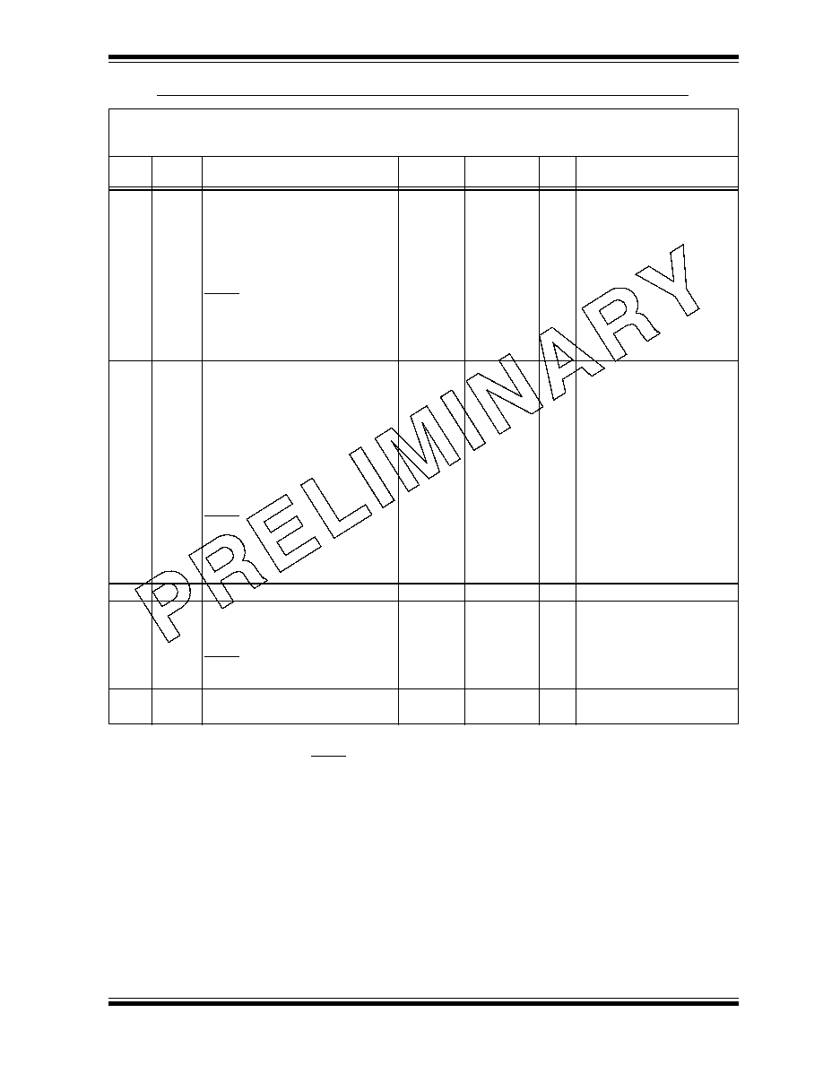
PIC18CXX2
©
7/99 Microchip Technology Inc.
Preliminary
DS39026B-page 247
21.3
DC Characteristics: PIC18CXX2 (Industrial, Extended) and PIC18LCXX2 (Industrial)
DC CHARACTERISTICS
Standard Operating Conditions (unless otherwise stated)
Operating temperature -40∞C
T
A
+85∞C for industrial
-40∞C
T
A
+125∞C for extended
Param
No.
Symbol
Characteristic
Min
Max
Units
Conditions
V
IL
Input Low Voltage
I/O ports:
D030
with TTL buffer
V
SS
0.15V
DD
V
V
DD
< 4.5V
D030A
--
0.8
V
4.5V
V
DD
5.5V
D031
with Schmitt Trigger buffer
RC3 and RC4
V
SS
V
SS
0.2V
DD
0.3V
DD
V
V
D032
MCLR
V
SS
0.2V
DD
V
D032A
OSC1 (in XT, HS and LP modes)
and T1OSI
V
SS
0.3V
DD
V
D033
OSC1(in RC mode)
(1)
V
SS
0.2V
DD
V
V
IH
Input High Voltage
I/O ports:
D040
with TTL buffer
0.25V
DD
+
0.8V
V
DD
V
V
DD
< 4.5V
D040A
2.0
V
DD
V
4.5V
V
DD
5.5V
D041
with Schmitt Trigger buffer
RC3 and RC4
0.8V
DD
0.7V
DD
V
DD
V
DD
V
V
D042
MCLR
0.8V
DD
V
DD
V
D042A
OSC1 (in XT, HS and LP modes)
and T1OSI
0.7V
DD
V
DD
V
D043
OSC1 (RC mode)
(1)
0.9V
DD
V
DD
V
D050
V
HYS
Hysteresis of Schmitt Trigger Inputs
TBD
TBD
V
I
IL
Input Leakage Current
(2,3)
D060
I/O ports
--
±
1
µ
A
V
SS
V
PIN
V
DD
,
Pin at hi-impedance
D061
MCLR
--
±
5
µ
A
Vss
V
PIN
V
DD
D063
OSC1
--
±
5
µ
A
Vss
V
PIN
V
DD
I
PU
Weak Pull-up Current
D070
I
PURB
PORTB weak pull-up current
50
400
µ
A
V
DD
= 5V, V
PIN
= V
SS
Note 1: In RC oscillator configuration, the OSC1/CLKIN pin is a Schmitt Trigger input. It is not recommended that the
PICmicro be driven with an external clock while in RC mode.
2: The leakage current on the MCLR pin is strongly dependent on the applied voltage level. The specified
levels represent normal operating conditions. Higher leakage current may be measured at different input
voltages.
3: Negative current is defined as current sourced by the pin.

PIC18CXX2
DS39026B-page 248
Preliminary
©
7/99 Microchip Technology Inc.
21.3
DC Characteristics: PIC18CXX2 (Industrial, Extended) and PIC18LCXX2 (Industrial) (cont'd)
DC CHARACTERISTICS
Standard Operating Conditions (unless otherwise stated)
Operating temperature
-40∞C
T
A
+85∞C for industrial
-40∞C
T
A
+125∞C for extended
Param
No.
Symbol
Characteristic
Min
Max
Units
Conditions
V
OL
Output Low Voltage
D080
I/O ports
--
0.6
V
I
OL
= 8.5 mA, V
DD
= 4.5V,
-40
∞
C to +85
∞
C
D080A
--
0.6
V
I
OL
= 7.0 mA, V
DD
= 4.5V,
-40
∞
C to +125
∞
C
D083
OSC2/CLKOUT
(RC mode)
--
0.6
V
I
OL
= 1.6 mA, V
DD
= 4.5V,
-40
∞
C to +85
∞
C
D083A
--
0.6
V
I
OL
= 1.2 mA, V
DD
= 4.5V,
-40
∞
C to +125
∞
C
V
OH
Output High Voltage
(3)
D090
I/O ports
V
DD
- 0.7
--
V
I
OH
= -3.0 mA, V
DD
= 4.5V,
-40
∞
C to +85
∞
C
D090A
V
DD
- 0.7
--
V
I
OH
= -2.5 mA, V
DD
= 4.5V,
-40
∞
C to +125
∞
C
D092
OSC2/CLKOUT
(RC mode)
V
DD
- 0.7
--
V
I
OH
= -1.3 mA, V
DD
= 4.5V,
-40
∞
C to +85
∞
C
D092A
V
DD
- 0.7
--
V
I
OH
= -1.0 mA, V
DD
= 4.5V,
-40
∞
C to +125
∞
C
D150
V
OD
Open-drain High Voltage
--
7.5
V
RA4 pin
Capacitive Loading Specs
on Output Pins
D101
C
IO
All I/O pins and OSC2
(in RC mode)
--
50
pF
To meet the AC Timing Specifications
D102
C
B
SCL, SDA
--
400
pF
In I
2
C mode
Note 1: In RC oscillator configuration, the OSC1/CLKIN pin is a Schmitt Trigger input. It is not recommended that the
PICmicro be driven with an external clock while in RC mode.
2: The leakage current on the MCLR pin is strongly dependent on the applied voltage level. The specified
levels represent normal operating conditions. Higher leakage current may be measured at different input
voltages.
3: Negative current is defined as current sourced by the pin.
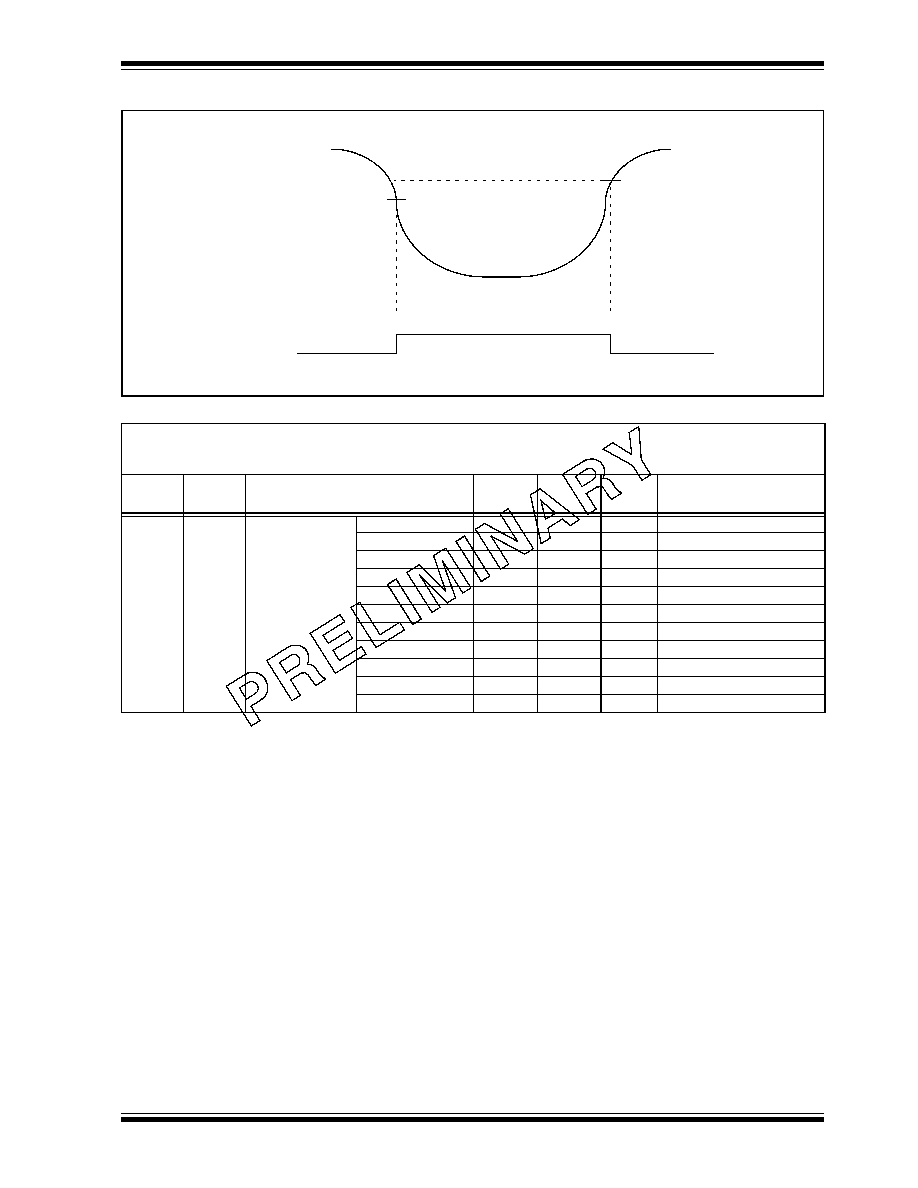
PIC18CXX2
©
7/99 Microchip Technology Inc.
Preliminary
DS39026B-page 249
FIGURE 21-3: LOW-VOLTAGE DETECT CHARACTERISTICS
TABLE 21-1:
LOW VOLTAGE DETECT CHARACTERISTICS
Standard Operating Conditions (unless otherwise stated)
Operating temperature
-40∞C
T
A
+85∞C for industrial
-40∞C
T
A
+125∞C for extended
Param
No.
Symbol
Characteristic
Min
Max
Units
Conditions
D420
V
LVD
LVD Voltage
LVV<3:0> =
0100
2.5
2.66
V
LVV<3:0> =
0101
2.7
2.86
V
LVV<3:0> =
0110
2.8
2.98
V
LVV<3:0> =
0111
3.0
3.2
V
LVV<3:0> =
1000
3.3
3.52
V
LVV<3:0> =
1001
3.5
3.72
V
LVV<3:0> =
1010
3.6
3.84
V
LVV<3:0> =
1011
3.8
4.04
V
LVV<3:0> =
1100
4.0
4.26
V
LVV<3:0> =
1101
4.2
4.46
V
LVV<3:0> =
1110
4.5
4.78
V
V
LVD
LVDIF
V
DD
(LVDIF set by hardware)
(LVDIF can be
cleared in software)
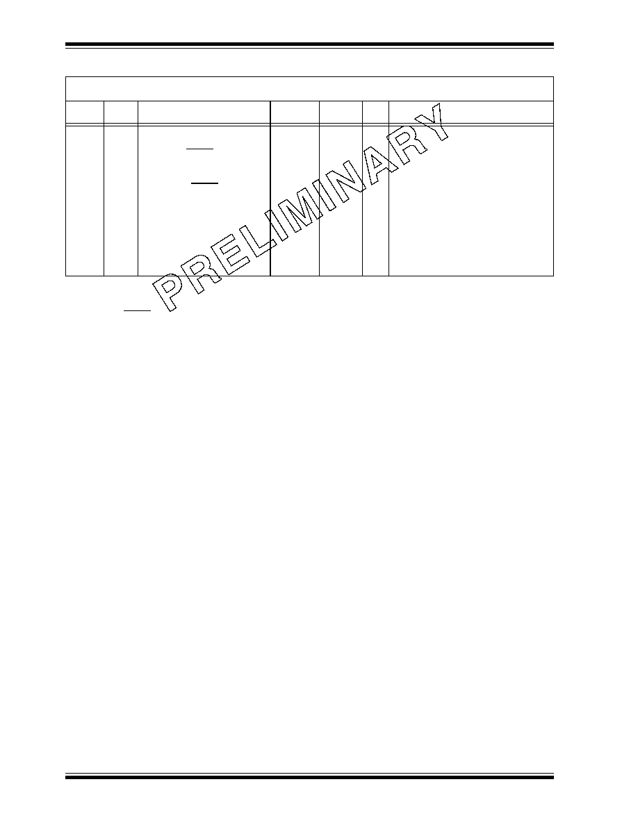
PIC18CXX2
DS39026B-page 250
Preliminary
©
7/99 Microchip Technology Inc.
TABLE 21-2:
EPROM PROGRAMMING REQUIREMENTS
DC CHARACTERISTICS
Standard Operating Conditions (unless otherwise stated)
Operating temperature
-40∞C
T
A
+40∞C
Param.
No.
Sym
Characteristic
Min
Max
Units
Conditions
Internal Program Memory
Programming Specs (Note 1)
D110
D111
D112
D113
D114
D115
V
PP
V
DDP
I
PP
I
DDP
T
PROG
T
ERASE
Voltage on MCLR/V
PP
pin
Supply voltage during
programming
Current into MCLR/V
PP
pin
Supply current during
programming
Programming pulse width
EPROM erase time
Device operation
3V
Device operation
3V
12.75
4.75
--
--
100
4
TBD
13.25
5.25
50
30
1000
--
--
V
V
mA
mA
µ
s
hrs
hrs
Note 2
Terminated via internal/external
interrupt or a reset
Note 1: These specifications are for the programming of the on-chip program memory EPROM through the use of the
table write instructions. The complete programming specifications can be found in: PIC18CXXX Program-
ming Specifications (Literature number TBD).
2: The MCLR/V
PP
pin may be kept in this range at times other than programming, but is not recommended.

PIC18CXX2
©
7/99 Microchip Technology Inc.
Preliminary
DS39026B-page 251
21.4
AC (Timing) Characteristics
21.4.1
TIMING PARAMETER SYMBOLOGY
The timing parameter symbols have been created fol-
lowing one of the following formats:
1. TppS2ppS
3. T
CC
:
ST
(I
2
C specifications only)
2. TppS
4. Ts
(I
2
C specifications only)
T
F
Frequency
T
Time
Lowercase letters (pp) and their meanings:
pp
cc
CCP1
osc
OSC1
ck
CLKOUT
rd
RD
cs
CS
rw
RD or WR
di
SDI
sc
SCK
do
SDO
ss
SS
dt
Data in
t0
T0CKI
io
I/O port
t1
T1CKI
mc
MCLR
wr
WR
Uppercase letters and their meanings:
S
F
Fall
P
Period
H
High
R
Rise
I
Invalid (Hi-impedance)
V
Valid
L
Low
Z
Hi-impedance
I
2
C only
AA
output access
High
High
BUF
Bus free
Low
Low
T
CC
:
ST
(I
2
C specifications only)
CC
HD
Hold
SU
Setup
ST
DAT
DATA input hold
STO
STOP condition
STA
START condition
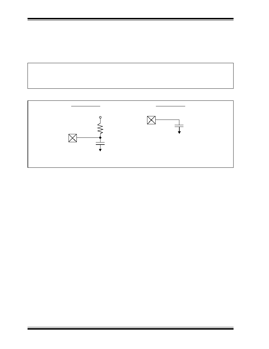
PIC18CXX2
DS39026B-page 252
Preliminary
©
7/99 Microchip Technology Inc.
21.4.2
TIMING CONDITIONS
The temperature and voltages specified in Table 21-3
apply to all timing specifications unless otherwise
noted. Figure 21-4 specifies the load conditions for the
timing specifications.
TABLE 21-3:
TEMPERATURE AND VOLTAGE SPECIFICATIONS - AC
FIGURE 21-4: LOAD CONDITIONS FOR DEVICE TIMING SPECIFICATIONS
AC CHARACTERISTICS
Standard Operating Conditions (unless otherwise stated)
Operating temperature -40∞C
T
A
+85∞C
for industrial
-40∞C
T
A
+125∞C
for extended
Operating voltage V
DD
range as described in DC spec Section 21.1 and Section 21.2.
LC parts operate for industrial temp's only.
V
DD
/2
C
L
R
L
Pin
Pin
V
SS
V
SS
C
L
R
L
= 464
C
L
= 50 pF
for all pins except OSC2/CLKOUT
and including D and E outputs as ports
Load condition 1
Load condition 2
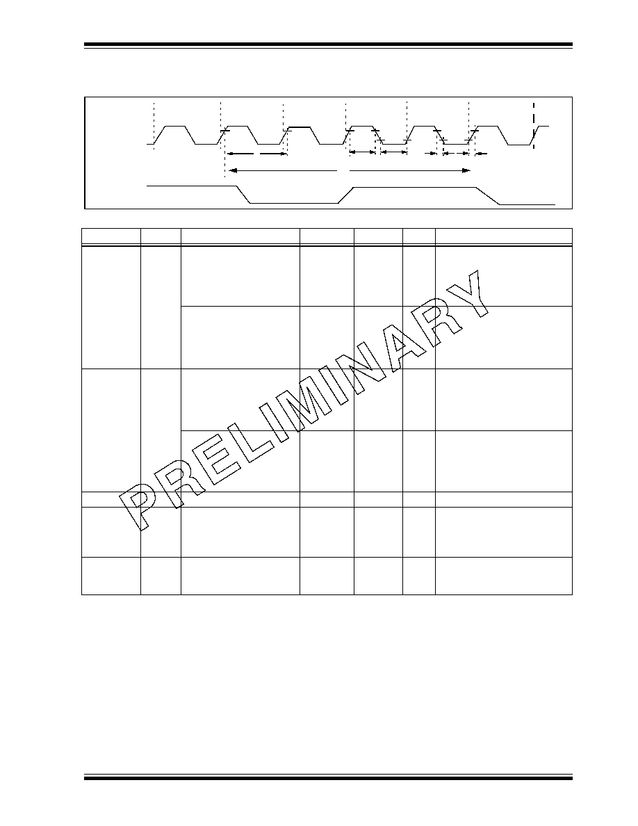
PIC18CXX2
©
7/99 Microchip Technology Inc.
Preliminary
DS39026B-page 253
21.4.3
TIMING DIAGRAMS AND SPECIFICATIONS
FIGURE 21-5: EXTERNAL CLOCK TIMING
TABLE 21-4:
EXTERNAL CLOCK TIMING REQUIREMENTS
Param. No.
Symbol Characteristic
Min
Max
Units Conditions
1A
Fosc
External CLKIN
Frequency
(1)
DC
40
MHz
XT 0osc
DC
40
MHz
HS osc
4
10
MHz
HS + PLL osc
DC
DC
40
40
kHz
MHz
LP osc
EC
Oscillator Frequency
(1)
DC
4
MHz
RC osc
0.1
4
MHz
XT osc
4
25
MHz
HS osc
4
10
MHz
HS + PLL osc
5
200
kHz
LP osc mode
1
Tosc
External CLKIN Period
(1)
250
--
ns
XT and RC osc
40
--
ns
HS osc
100
--
ns
HS + PLL osc
5
5
--
--
µ
s
ns
LP osc
EC
Oscillator Period
(1)
250
--
ns
RC osc
250
10,000
ns
XT osc
100
40
10,000
100
ns
ns
HS osc
HS + PLL osc
5
--
µ
s
LP osc
2
T
CY
Instruction Cycle Time
(1)
100
--
ns
T
CY
= 4/F
OSC
3
TosL,
TosH
External Clock in (OSC1)
High or Low Time
30
--
ns
XT osc
2.5
--
µ
s
LP osc
10
--
ns
HS osc
4
TosR,
TosF
External Clock in (OSC1)
Rise or Fall Time
--
20
ns
XT osc
--
50
ns
LP osc
--
7.5
ns
HS osc
Note 1: Instruction cycle period (T
CY
) equals four times the input oscillator time-base period. All specified values are
based on characterization data for that particular oscillator type under standard operating conditions with the
device executing code. Exceeding these specified limits may result in an unstable oscillator operation and/or
higher than expected current consumption. All devices are tested to operate at "min." values with an external
clock applied to the OSC1/CLKIN pin. When an external clock input is used, the "Max." cycle time limit is
"DC" (no clock) for all devices.
OSC1
CLKOUT
Q4
Q1
Q2
Q3
Q4
Q1
1
2
3
3
4
4

PIC18CXX2
DS39026B-page 254
Preliminary
©
7/99 Microchip Technology Inc.
TABLE 21-5:
PLL CLOCK TIMING SPECIFICATION (V
DD
= 4.2V - 5.5V)
Param
No.
Symbol Characteristic
Min
Max
Units Conditions
T
RC
PLL Start-up Time
(Lock Time)
--
2
ms
CLK
CLKOUT Stability (Jitter) using PLL
-2
+2
%
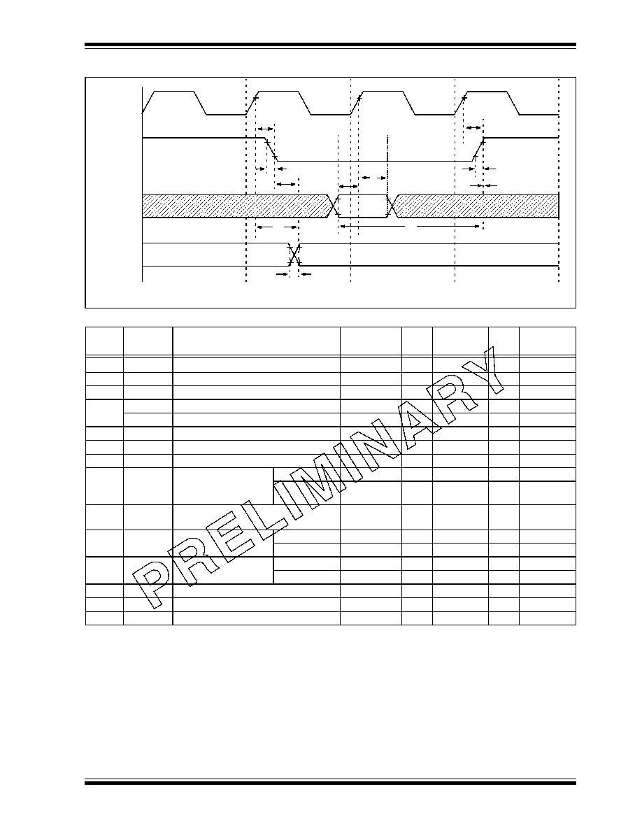
PIC18CXX2
©
7/99 Microchip Technology Inc.
Preliminary
DS39026B-page 255
FIGURE 21-6: CLKOUT AND I/O TIMING
TABLE 21-6:
CLKOUT AND I/O TIMING REQUIREMENTS
Param.
No.
Symbol
Characteristic
Min
Typ
Max
Units Conditions
10
TosH2ckL OSC1
to CLKOUT
--
75
200
ns
(1)
11
TosH2ckH OSC1
to CLKOUT
--
75
200
ns
(1)
12
TckR
CLKOUT rise time
--
35
100
ns
(1)
13
TckF
CLKOUT fall time
--
35
100
ns
(1)
14
TckL2ioV
CLKOUT
to Port out valid
--
--
0.5T
CY
+ 20
ns
(1)
15
TioV2ckH Port in valid before CLKOUT
0.25T
CY
+ 25
--
--
ns
(1)
16
TckH2ioI
Port in hold after CLKOUT
0
--
--
ns
(1)
17
TosH2ioV
OSC1
(Q1 cycle) to Port out valid
--
50
150
ns
18
TosH2ioI
OSC1
(Q2 cycle) to
Port input invalid
(I/O in hold time)
PIC18CXXX
100
--
--
ns
18A
PIC18LCXXX
200
--
--
ns
19
TioV2osH Port input valid to OSC1
(I/O in setup time)
0
--
--
ns
20
TioR
Port output rise time
PIC18CXXX
--
10
25
ns
20A
PIC18LCXXX
--
--
60
ns
21
TioF
Port output fall time
PIC18CXXX
--
10
25
ns
21A
PIC18LCXXX
--
--
60
ns
22
T
INP
INT pin high or low time
T
CY
--
--
ns
23
T
RBP
RB7:RB4 change INT high or low time
T
CY
--
--
ns
24
T
RCP
RC7:RC4 change INT high or low time
20
ns
These parameters are asynchronous events not related to any internal clock edges.
Note 1: Measurements are taken in RC Mode where CLKOUT output is 4 x T
OSC
.
Note: Refer to Figure 21-4 for load conditions
.
OSC1
CLKOUT
I/O Pin
(input)
I/O Pin
(output)
Q4
Q1
Q2
Q3
10
13
14
17
20,
21
19
18
15
11
12
16
old value
new value
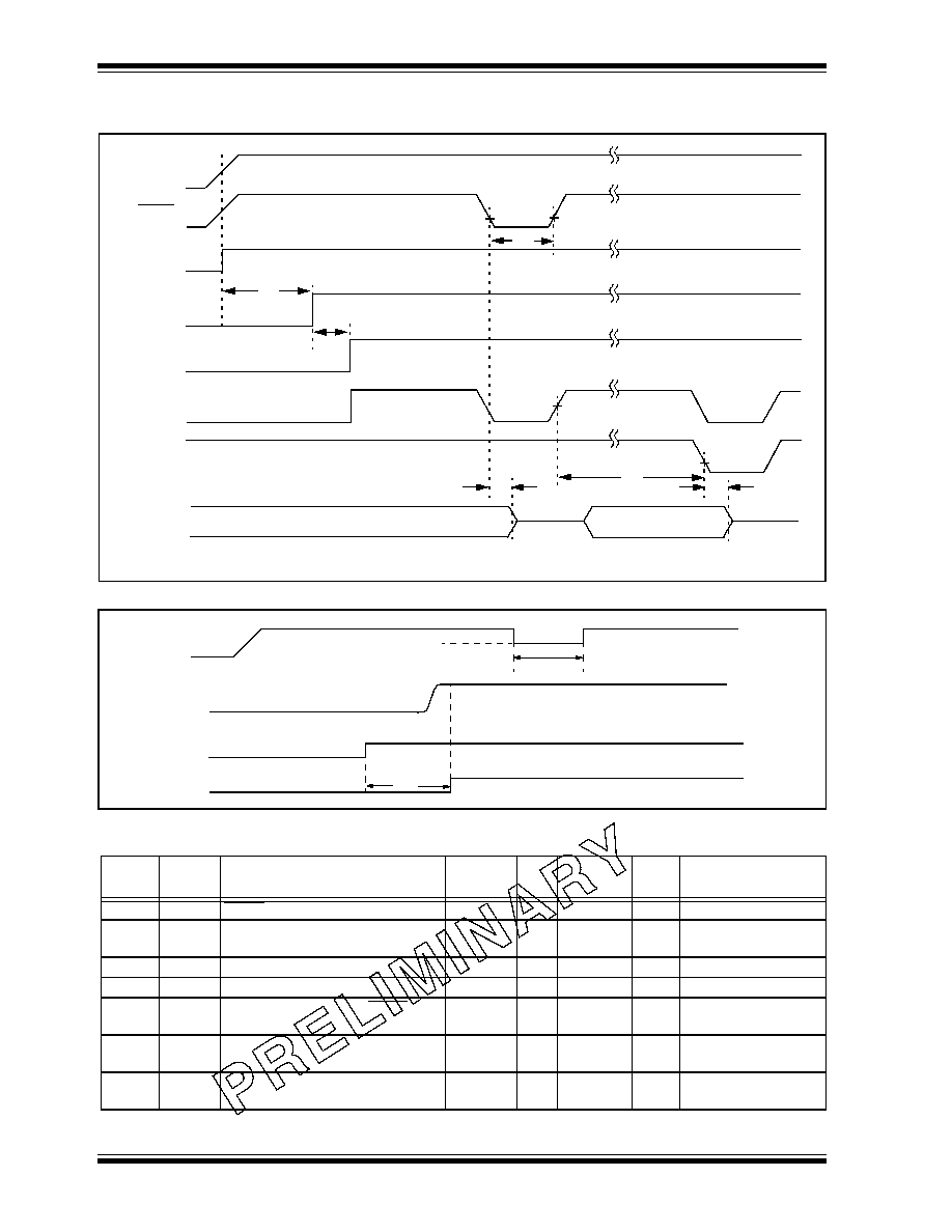
PIC18CXX2
DS39026B-page 256
Preliminary
©
7/99 Microchip Technology Inc.
FIGURE 21-7: RESET, WATCHDOG TIMER, OSCILLATOR START-UP TIMER AND POWER-UP
TIMER TIMING
FIGURE 21-8: BROWN-OUT RESET TIMING
TABLE 21-7:
RESET, WATCHDOG TIMER, OSCILLATOR START-UP TIMER, POWER-UP TIMER
AND BROWN-OUT RESET REQUIREMENTS
Param.
No.
Symbol
Characteristic
Min
Typ
Max
Units
Conditions
30
TmcL
MCLR Pulse Width (low)
2
--
--
µ
s
31
T
WDT
Watchdog Timer Time-out Period
(No Prescaler)
7
18
33
ms
32
T
OST
Oscillation Start-up Timer Period
1024T
OSC
--
1024T
OSC
--
T
OSC
= OSC1 period
33
T
PWRT
Power up Timer Period
28
72
132
ms
34
T
IOZ
I/O Hi-impedance from MCLR Low
or Watchdog Timer Reset
--
2
--
µ
s
35
T
BOR
Brown-out Reset Pulse Width
200
--
--
µ
s
V
DD
B
VDD
(See
D005)
36
T
IVRST
Time for Internal Reference
Voltage to become stable
--
20
50
µ
s
V
DD
MCLR
Internal
POR
PWRT
Time-out
OSC
Time-out
Internal
Reset
Watchdog
Timer
Reset
33
32
30
31
34
I/O Pins
34
Note: Refer to Figure 21-4 for load conditions.
V
DD
BV
DD
35
V
BGAP
= 1.2V
V
IRVST
Enable Internal Reference Voltage
Internal Reference Voltage stable
36
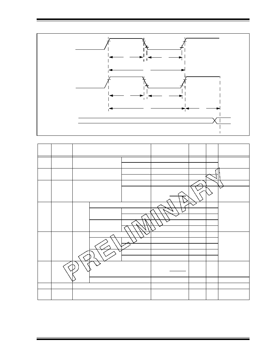
PIC18CXX2
©
7/99 Microchip Technology Inc.
Preliminary
DS39026B-page 257
FIGURE 21-9: TIMER0 AND TIMER1 EXTERNAL CLOCK TIMINGS
TABLE 21-8:
TIMER0 AND TIMER1 EXTERNAL CLOCK REQUIREMENTS
Param
No.
Symbol
Characteristic
Min
Max
Units
Conditions
40
Tt0H
T0CKI High Pulse Width
No Prescaler
0.5T
CY
+ 20
--
ns
With Prescaler
10
--
ns
41
Tt0L
T0CKI Low Pulse Width
No Prescaler
0.5T
CY
+ 20
--
ns
With Prescaler
10
--
ns
42
Tt0P
T0CKI Period
No Prescaler
T
CY
+ 10
--
ns
With Prescaler
Greater of:
20 n
S
or T
CY
+ 40
N
--
ns
N = prescale
value
(1, 2, 4,..., 256)
45
Tt1H
T1CKI
High
Time
Synchronous, no prescaler
0.5T
CY
+ 20
--
ns
Synchronous,
with prescaler
PIC18CXXX
10
--
ns
PIC18LCXXX
25
--
ns
Asynchronous
PIC18CXXX
30
--
ns
PIC18LCXXX
50
--
ns
46
Tt1L
T1CKI
Low
Time
Synchronous, no prescaler
0.5T
CY
+ 5
--
ns
Synchronous,
with prescaler
PIC18CXXX
10
--
ns
PIC18LCXXX
25
--
ns
Asynchronous
PIC18CXXX
30
--
ns
PIC18LCXXX
TBD
TBD
ns
47
Tt1P
T1CKI
input
period
Synchronous
Greater of:
20 n
S
or T
CY
+ 40
N
--
ns
N = prescale
value
(1, 2, 4, 8)
Asynchronous
60
--
ns
Ft1
T1CKI oscillator input frequency range
DC
50
kHz
48
Tcke2tmrI Delay from external T1CKI clock edge to
timer increment
2Tosc
7Tosc
--
Note: Refer to Figure 21-4 for load conditions.
46
47
45
48
41
42
40
T0CKI
T1OSO/T1CKI
TMR0 or
TMR1
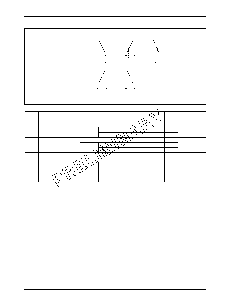
PIC18CXX2
DS39026B-page 258
Preliminary
©
7/99 Microchip Technology Inc.
FIGURE 21-10: CAPTURE/COMPARE/PWM TIMINGS (CCP1 AND CCP2)
TABLE 21-9:
CAPTURE/COMPARE/PWM REQUIREMENTS (CCP1 AND CCP2)
Param.
No.
Symbol
Characteristic
Min
Max
Units
Conditions
50
TccL
CCPx input low
time
No Prescaler
0.5T
CY
+ 20
--
ns
With
Prescaler
PIC18CXXX
10
--
ns
PIC18LCXXX
20
--
ns
51
TccH
CCPx input
high time
No Prescaler
0.5T
CY
+ 20
--
ns
With
Prescaler
PIC18CXXX
10
--
ns
PIC18LCXXX
20
--
ns
52
TccP
CCPx input period
3T
CY
+ 40
N
--
ns
N = prescale
value (1,4 or 16)
53
TccR
CCPx output fall time
PIC18CXXX
--
25
ns
PIC18LCXXX
--
45
ns
54
TccF
CCPx output fall time
PIC18CXXX
--
25
ns
PIC18LCXXX
--
45
ns
Note: Refer to Figure 21-4 for load conditions.
CCPx
(Capture Mode)
50
51
52
CCPx
53
54
(Compare or PWM Mode)
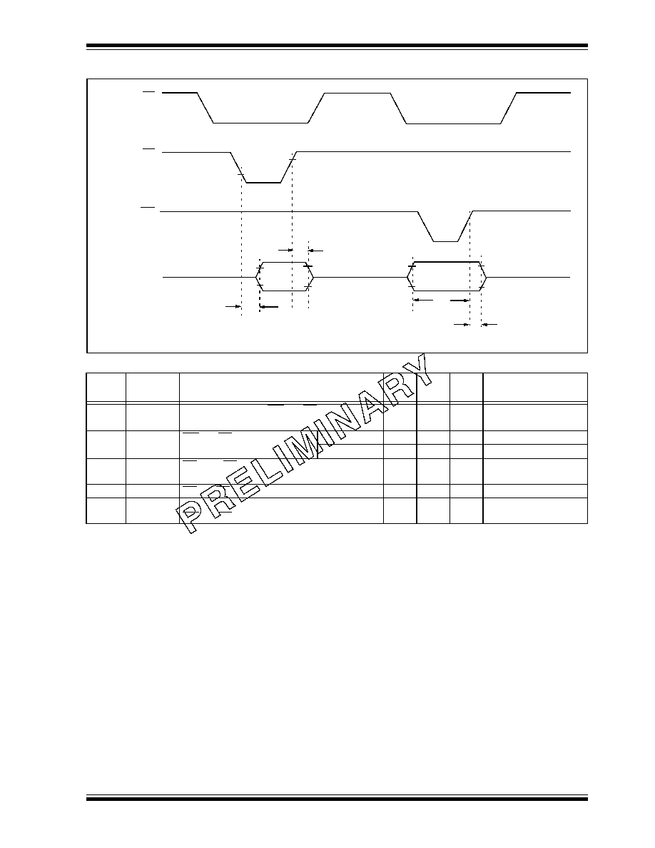
PIC18CXX2
©
7/99 Microchip Technology Inc.
Preliminary
DS39026B-page 259
FIGURE 21-11: PARALLEL SLAVE PORT TIMING (PIC18C4X2)
TABLE 21-10: PARALLEL SLAVE PORT REQUIREMENTS (PIC18C4X2)
Param.
No.
Symbol
Characteristic
Min
Max
Units
Conditions
62
TdtV2wrH
Data in valid before WR
or CS
(setup time)
20
25
--
--
ns
ns
Extended Temp range
63
TwrH2dtI
WR
or CS
to data≠in invalid
(hold time)
PIC18CXXX
20
--
ns
PIC18LCXXX
35
--
ns
64
TrdL2dtV
RD
and CS
to data≠out valid
--
--
80
90
ns
ns
Extended Temp range
65
TrdH2dtI
RD
or CS
to data≠out invalid
10
30
ns
66
TibfINH
Inhibit of the IBF flag bit being cleared from
WR
or CS
--
3T
CY
Note: Refer to Figure 21-4 for load conditions.
RE2/CS
RE0/RD
RE1/WR
RD7:RD0
62
63
64
65
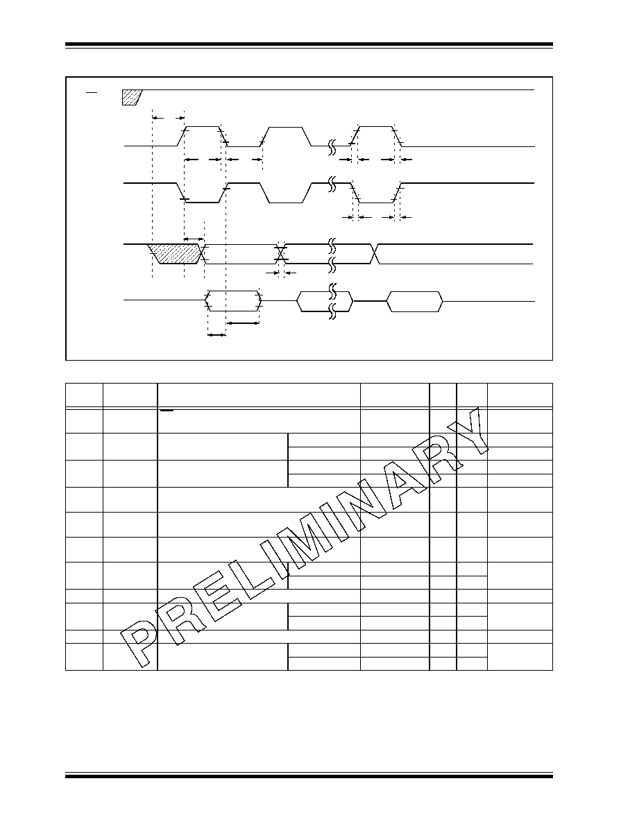
PIC18CXX2
DS39026B-page 260
Preliminary
©
7/99 Microchip Technology Inc.
FIGURE 21-12: EXAMPLE SPI MASTER MODE TIMING (CKE = 0)
TABLE 21-11: EXAMPLE SPI MODE REQUIREMENTS (MASTER MODE, CKE = 0)
Param.
No.
Symbol
Characteristic
Min
Max Units
Conditions
70
TssL2scH,
TssL2scL
SS
to SCK
or SCK
input
T
CY
--
ns
71
TscH
SCK input high time
(slave mode)
Continuous
1.25T
CY
+ 30
--
ns
71A
Single Byte
40
--
ns
Note 1
72
TscL
SCK input low time
(slave mode)
Continuous
1.25T
CY
+ 30
--
ns
72A
Single Byte
40
--
ns
Note 1
73
TdiV2scH,
TdiV2scL
Setup time of SDI data input to SCK edge
100
--
ns
73A
T
B
2
B
Last clock edge of Byte1 to the 1st clock edge of
Byte2
1.5T
CY
+ 40
--
ns
Note 2
74
TscH2diL,
TscL2diL
Hold time of SDI data input to SCK edge
100
--
ns
75
TdoR
SDO data output rise time
PIC18CXXX
--
25
ns
PIC18LCXXX
--
45
ns
76
TdoF
SDO data output fall time
--
25
ns
78
TscR
SCK output rise time
(master mode)
PIC18CXXX
--
25
ns
PIC18LCXXX
--
45
ns
79
TscF
SCK output fall time (master mode)
--
25
ns
80
TscH2doV,
TscL2doV
SDO data output valid after
SCK edge
PIC18CXXX
--
50
ns
PIC18LCXXX
--
100
ns
Note 1: Requires the use of Parameter # 73A.
2: Only if Parameter #s 71A and 72A are used.
SS
SCK
(CKP = 0)
SCK
(CKP = 1)
SDO
SDI
70
71
72
73
74
75, 76
78
79
80
79
78
MSb
LSb
BIT6 - - - - - -1
MSb IN
LSb IN
BIT6 - - - -1
Note: Refer to Figure 21-4 for load conditions.
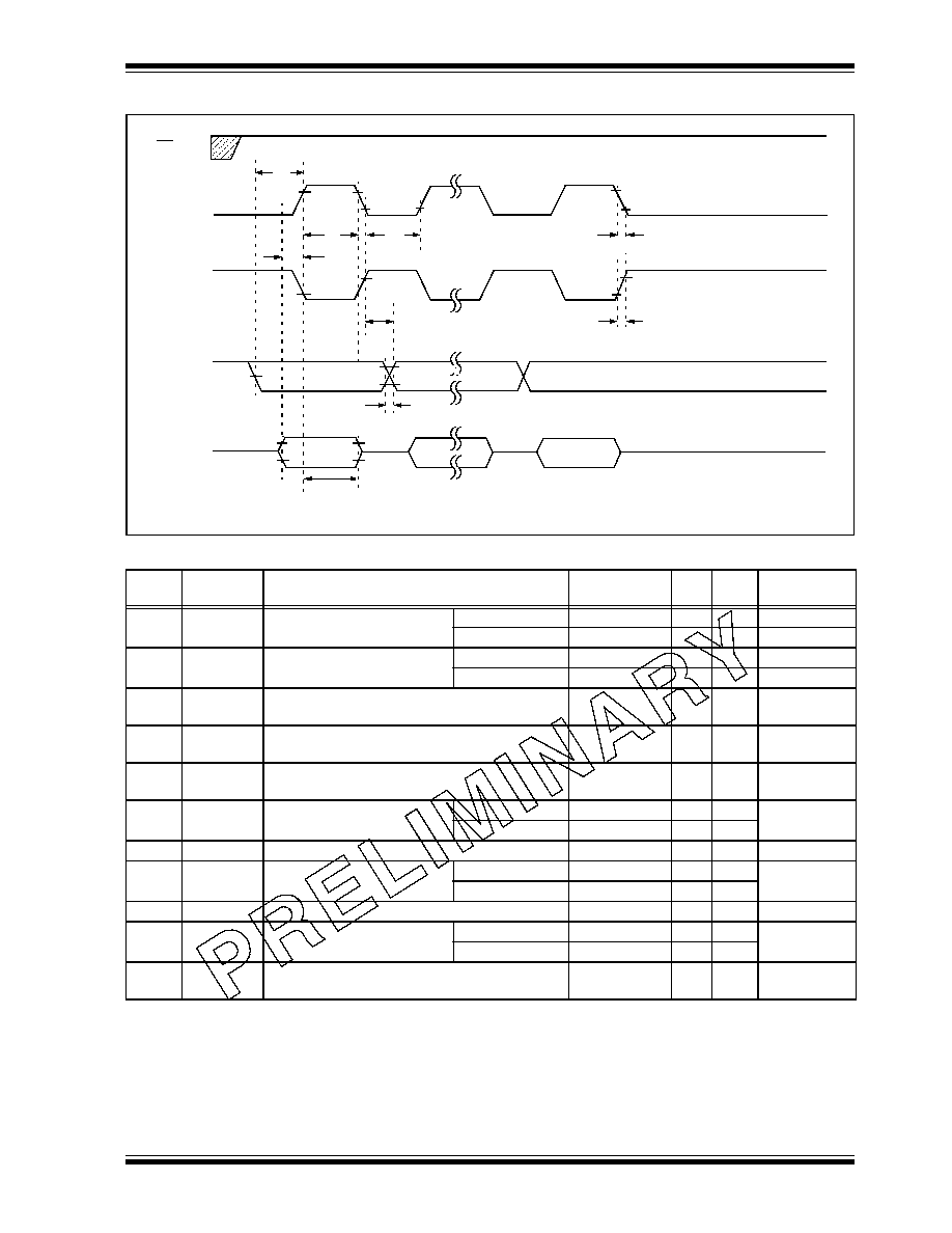
PIC18CXX2
©
7/99 Microchip Technology Inc.
Preliminary
DS39026B-page 261
FIGURE 21-13: EXAMPLE SPI MASTER MODE TIMING (CKE = 1)
TABLE 21-12: EXAMPLE SPI MODE REQUIREMENTS (MASTER MODE, CKE = 1)
Param.
No.
Symbol
Characteristic
Min
Max Units
Conditions
71
TscH
SCK input high time
(slave mode)
Continuous
1.25T
CY
+ 30
--
ns
71A
Single Byte
40
--
ns
Note 1
72
TscL
SCK input low time
(slave mode)
Continuous
1.25T
CY
+ 30
--
ns
72A
Single Byte
40
--
ns
Note 1
73
TdiV2scH,
TdiV2scL
Setup time of SDI data input to SCK edge
100
--
ns
73A
T
B
2
B
Last clock edge of Byte1 to the 1st clock edge of
Byte2
1.5T
CY
+ 40
--
ns
Note 2
74
TscH2diL,
TscL2diL
Hold time of SDI data input to SCK edge
100
--
ns
75
TdoR
SDO data output rise time
PIC18CXXX
--
25
ns
PIC18LCXXX
45
ns
76
TdoF
SDO data output fall time
--
25
ns
78
TscR
SCK output rise time
(master mode)
PIC18CXXX
--
25
ns
PIC18LCXXX
45
ns
79
TscF
SCK output fall time (master mode)
--
25
ns
80
TscH2doV,
TscL2doV
SDO data output valid after
SCK edge
PIC18CXXX
--
50
ns
PIC18LCXXX
100
ns
81
TdoV2scH,
TdoV2scL
SDO data output setup to SCK edge
T
CY
--
ns
Note 1: Requires the use of Parameter # 73A.
2: Only if Parameter #s 71A and 72A are used.
SS
SCK
(CKP = 0)
SCK
(CKP = 1)
SDO
SDI
81
71
72
74
75, 76
78
80
MSb
79
73
MSb IN
BIT6 - - - - - -1
LSb IN
BIT6 - - - -1
LSb
Note: Refer to Figure 21-4 for load conditions.
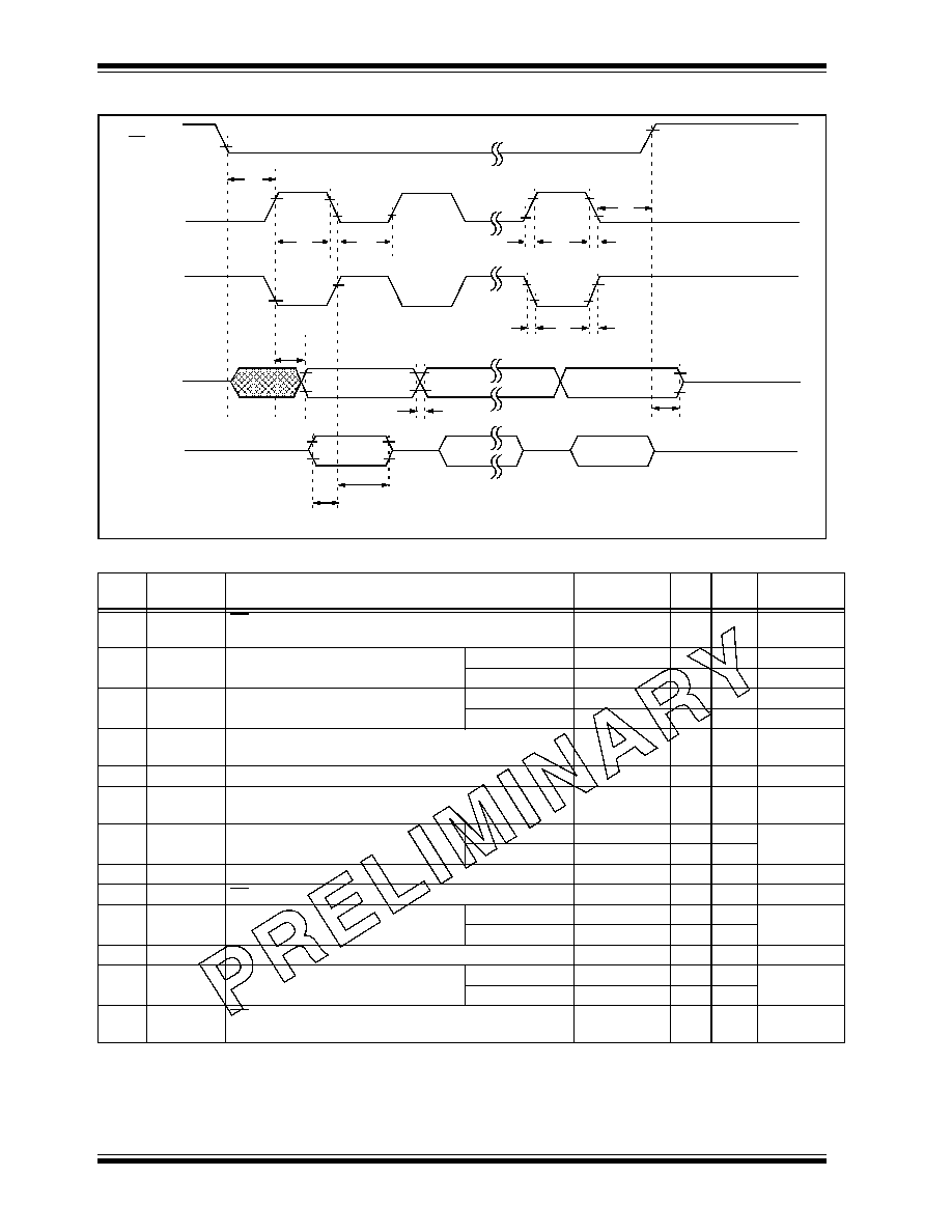
PIC18CXX2
DS39026B-page 262
Preliminary
©
7/99 Microchip Technology Inc.
FIGURE 21-14: EXAMPLE SPI SLAVE MODE TIMING (CKE = 0)
TABLE 21-13: EXAMPLE SPI MODE REQUIREMENTS (SLAVE MODE TIMING (CKE = 0))
Parm.
No.
Symbol
Characteristic
Min
Max Units Conditions
70
TssL2scH,
TssL2scL
SS
to SCK
or SCK
input
T
CY
--
ns
71
TscH
SCK input high time
(slave mode)
Continuous
1.25T
CY
+ 30
--
ns
71A
Single Byte
40
--
ns
Note 1
72
TscL
SCK input low time
(slave mode)
Continuous
1.25T
CY
+ 30
--
ns
72A
Single Byte
40
--
ns
Note 1
73
TdiV2scH,
TdiV2scL
Setup time of SDI data input to SCK edge
100
--
ns
73A
T
B
2
B
Last clock edge of Byte1 to the 1st clock edge of Byte2
1.5T
CY
+ 40
--
ns
Note 2
74
TscH2diL,
TscL2diL
Hold time of SDI data input to SCK edge
100
--
ns
75
TdoR
SDO data output rise time
PIC18CXXX
--
25
ns
PIC18LCXXX
45
ns
76
TdoF
SDO data output fall time
--
25
ns
77
TssH2doZ
SS
to SDO output hi-impedance
10
50
ns
78
TscR
SCK output rise time
(master mode)
PIC18CXXX
--
25
ns
PIC18LCXXX
45
ns
79
TscF
SCK output fall time (master mode)
--
25
ns
80
TscH2doV,
TscL2doV
SDO data output valid after SCK
edge
PIC18CXXX
--
50
ns
PIC18LCXXX
100
ns
83
TscH2ssH,
TscL2ssH
SS
after SCK edge
1.5T
CY
+ 40
--
ns
Note 1: Requires the use of Parameter # 73A.
2: Only if Parameter #s 71A and 72A are used.
SS
SCK
(CKP = 0)
SCK
(CKP = 1)
SDO
SDI
70
71
72
73
74
75, 76
77
78
79
80
79
78
SDI
MSb
LSb
BIT6 - - - - - -1
MSb IN
BIT6 - - - -1
LSb IN
83
Note: Refer to Figure 21-4 for load conditions.
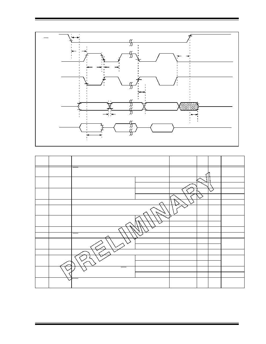
PIC18CXX2
©
7/99 Microchip Technology Inc.
Preliminary
DS39026B-page 263
FIGURE 21-15: EXAMPLE SPI SLAVE MODE TIMING (CKE = 1)
TABLE 21-14: EXAMPLE SPI SLAVE MODE REQUIREMENTS (CKE = 1)
Parm.
No.
Symbol
Characteristic
Min
Max Units Conditions
70
TssL2scH,
TssL2scL
SS
to SCK
or SCK
input
T
CY
--
ns
71
TscH
SCK input high time
(slave mode)
Continuous
1.25T
CY
+ 30
--
ns
71A
Single Byte
40
--
ns
Note 1
72
TscL
SCK input low time
(slave mode)
Continuous
1.25T
CY
+ 30
--
ns
72A
Single Byte
40
--
ns
Note 1
73A
T
B
2
B
Last clock edge of Byte1 to the 1st clock edge of Byte2
1.5T
CY
+ 40
--
ns
Note 2
74
TscH2diL,
TscL2diL
Hold time of SDI data input to SCK edge
100
--
ns
75
TdoR
SDO data output rise time
PIC18CXXX
--
25
ns
PIC18LCXXX
45
ns
76
TdoF
SDO data output fall time
--
25
ns
77
TssH2doZ
SS
to SDO output hi-impedance
10
50
ns
78
TscR
SCK output rise time
(master mode)
PIC18CXXX
--
25
ns
PIC18LCXXX
--
45
ns
79
TscF
SCK output fall time (master mode)
--
25
ns
80
TscH2doV,
TscL2doV
SDO data output valid after SCK
edge
PIC18CXXX
--
50
ns
PIC18LCXXX
--
100
ns
82
TssL2doV
SDO data output valid after SS
edge
PIC18CXXX
--
50
ns
PIC18LCXXX
--
100
ns
83
TscH2ssH,
TscL2ssH
SS
after SCK edge
1.5T
CY
+ 40
--
ns
Note 1: Requires the use of Parameter # 73A.
2: Only if Parameter #s 71A and 72A are used.
SS
SCK
(CKP = 0)
SCK
(CKP = 1)
SDO
SDI
70
71
72
82
SDI
74
75, 76
MSb
BIT6 - - - - - -1
LSb
77
MSb IN
BIT6 - - - -1
LSb IN
80
83
Note: Refer to Figure 21-4 for load conditions.
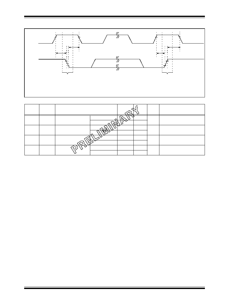
PIC18CXX2
DS39026B-page 264
Preliminary
©
7/99 Microchip Technology Inc.
FIGURE 21-16: I
2
C BUS START/STOP BITS TIMING
TABLE 21-15: I
2
C BUS START/STOP BITS REQUIREMENTS (SLAVE MODE)
Parm.
No.
Symbol
Characteristic
Min
Max
Units
Conditions
90
T
SU
:
STA
START condition
100 kHz mode
4700
--
ns
Only relevant for repeated
START condition
Setup time
400 kHz mode
600
--
91
T
HD
:
STA
START condition
100 kHz mode
4000
--
ns
After this period the first
clock pulse is generated
Hold time
400 kHz mode
600
--
92
T
SU
:
STO
STOP condition
100 kHz mode
4700
--
ns
Setup time
400 kHz mode
600
--
93
T
HD
:
STO
STOP condition
100 kHz mode
4000
--
ns
Hold time
400 kHz mode
600
--
Note: Refer to Figure 21-4 for load conditions.
91
92
93
SCL
SDA
START
Condition
STOP
Condition
90
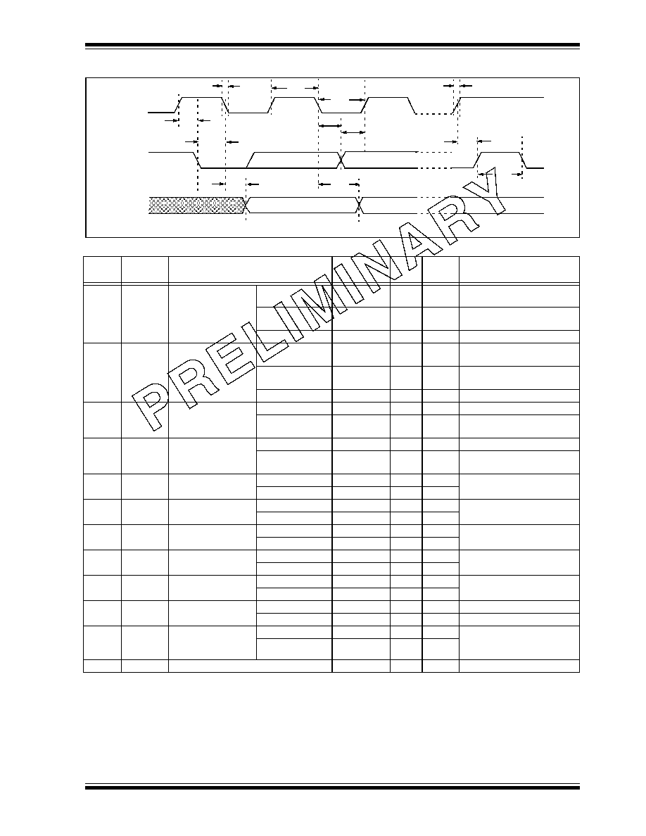
PIC18CXX2
©
7/99 Microchip Technology Inc.
Preliminary
DS39026B-page 265
FIGURE 21-17: I
2
C BUS DATA TIMING
TABLE 21-16: I
2
C BUS DATA REQUIREMENTS (SLAVE MODE)
Param.
No.
Symbol
Characteristic
Min
Max
Units
Conditions
100
T
HIGH
Clock high time
100 kHz mode
4.0
--
µ
s
PIC18CXXX must operate at a
minimum of 1.5 MHz
400 kHz mode
0.6
--
µ
s
PIC18CXXX must operate at a
minimum of 10 MHz
SSP Module
1.5T
CY
--
101
T
LOW
Clock low time
100 kHz mode
4.7
--
µ
s
PIC18CXXX must operate at a
minimum of 1.5 MHz
400 kHz mode
1.3
--
µ
s
PIC18CXXX must operate at a
minimum of 10 MHz
SSP Module
1.5T
CY
--
102
T
R
SDA and SCL rise
time
100 kHz mode
--
1000
ns
400 kHz mode
20 + 0.1Cb
300
ns
Cb is specified to be from
10 to 400 pF
103
T
F
SDA and SCL fall
time
100 kHz mode
--
300
ns
400 kHz mode
20 + 0.1Cb
300
ns
Cb is specified to be from
10 to 400 pF
90
T
SU
:
STA
START condition
setup time
100 kHz mode
4.7
--
µ
s
Only relevant for repeated
START condition
400 kHz mode
0.6
--
µ
s
91
T
HD
:
STA
START condition hold
time
100 kHz mode
4.0
--
µ
s
After this period the first clock
pulse is generated
400 kHz mode
0.6
--
µ
s
106
T
HD
:
DAT
Data input hold time
100 kHz mode
0
--
ns
400 kHz mode
0
0.9
µ
s
107
T
SU
:
DAT
Data input setup time
100 kHz mode
250
--
ns
Note 2
400 kHz mode
100
--
ns
92
T
SU
:
STO
STOP condition
setup time
100 kHz mode
4.7
--
µ
s
400 kHz mode
0.6
--
µ
s
109
T
AA
Output valid from
clock
100 kHz mode
--
3500
ns
Note 1
400 kHz mode
--
--
ns
110
T
BUF
Bus free time
100 kHz mode
4.7
--
µ
s
Time the bus must be free
before a new transmission can
start
400 kHz mode
1.3
--
µ
s
D102
Cb
Bus capacitive loading
--
400
pF
Note 1:
As a transmitter, the device must provide this internal minimum delay time to bridge the undefined region (min. 300 ns) of
the falling edge of SCL to avoid unintended generation of START or STOP conditions.
2: A fast-mode I
2
C bus device can be used in a standard-mode I
2
C bus system, but the requirement tsu;DAT
250 ns must
then be met. This will automatically be the case if the device does not stretch the LOW period of the SCL signal. If such a
device does stretch the LOW period of the SCL signal, it must output the next data bit to the SDA line.
T
R
max. + tsu;DAT = 1000 + 250 = 1250 ns (according to the standard-mode I
2
C bus specification) before the SCL line is
released.
Note: Refer to Figure 21-4 for load conditions
.
90
91
92
100
101
103
106
107
109
109
110
102
SCL
SDA
In
SDA
Out
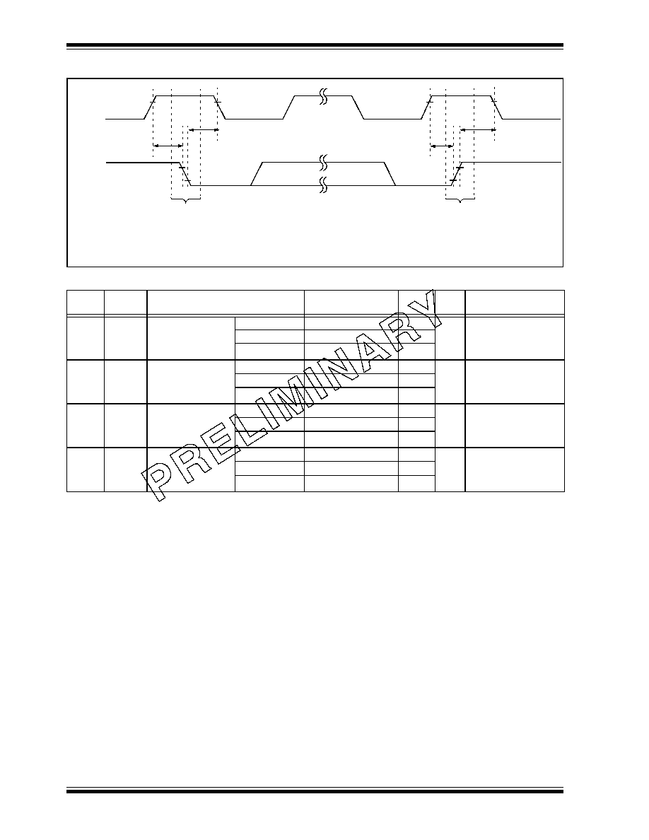
PIC18CXX2
DS39026B-page 266
Preliminary
©
7/99 Microchip Technology Inc.
FIGURE 21-18: MASTER SSP I
2
C BUS START/STOP BITS TIMING WAVEFORMS
TABLE 21-17: MASTER SSP I
2
C BUS START/STOP BITS REQUIREMENTS
Param.
No.
Symbol
Characteristic
Min
Max
Units
Conditions
90
T
SU
:
STA
START condition
100 kHz mode 2(T
OSC
)(BRG + 1)
--
ns
Only relevant for
repeated START
condition
Setup time
400 kHz mode 2(T
OSC
)(BRG + 1)
--
1 MHz mode
(1)
2(T
OSC
)(BRG + 1)
--
91
T
HD
:
STA
START condition
100 kHz mode 2(T
OSC
)(BRG + 1)
--
ns
After this period the
first clock pulse is
generated
Hold time
400 kHz mode 2(T
OSC
)(BRG + 1)
--
1 MHz mode
(1)
2(T
OSC
)(BRG + 1)
--
92
T
SU
:
STO
STOP condition
100 kHz mode 2(T
OSC
)(BRG + 1)
--
ns
Setup time
400 kHz mode 2(T
OSC
)(BRG + 1)
--
1 MHz mode
(1)
2(T
OSC
)(BRG + 1)
--
93
T
HD
:
STO
STOP condition
100 kHz mode 2(T
OSC
)(BRG + 1)
--
ns
Hold time
400 kHz mode 2(T
OSC
)(BRG + 1)
--
1 MHz mode
(1)
2(T
OSC
)(BRG + 1)
--
Note 1: Maximum pin capacitance = 10 pF for all I
2
C pins.
Note: Refer to Figure 21-4 for load conditions.
91
93
SCL
SDA
START
Condition
STOP
Condition
90
92
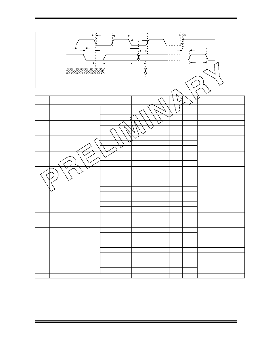
PIC18CXX2
©
7/99 Microchip Technology Inc.
Preliminary
DS39026B-page 267
FIGURE 21-19: MASTER SSP I
2
C BUS DATA TIMING
TABLE 21-18: MASTER SSP I
2
C BUS DATA REQUIREMENTS
Param.
No.
Symbol
Characteristic
Min
Max
Units
Conditions
100
T
HIGH
Clock high time
100 kHz mode
2(T
OSC
)(BRG + 1)
--
ms
400 kHz mode
2(T
OSC
)(BRG + 1)
--
ms
1 MHz mode
(1)
2(T
OSC
)(BRG + 1)
--
ms
101
T
LOW
Clock low time
100 kHz mode
2(T
OSC
)(BRG + 1)
--
ms
400 kHz mode
2(T
OSC
)(BRG + 1)
--
ms
1 MHz mode
(1)
2(T
OSC
)(BRG + 1)
--
ms
102
T
R
SDA and SCL
rise time
100 kHz mode
--
1000
ns
Cb is specified to be from
10 to 400 pF
400 kHz mode
20 + 0.1Cb
300
ns
1 MHz mode
(1)
--
300
ns
103
T
F
SDA and SCL
fall time
100 kHz mode
--
300
ns
Cb is specified to be from
10 to 400 pF
400 kHz mode
20 + 0.1Cb
300
ns
1 MHz mode
(1)
--
100
ns
90
T
SU
:
STA
START condition
setup time
100 kHz mode
2(T
OSC
)(BRG + 1)
--
ms
Only relevant for repeated
START condition
400 kHz mode
2(T
OSC
)(BRG + 1)
--
ms
1 MHz mode
(1)
2(T
OSC
)(BRG + 1)
--
ms
91
T
HD
:
STA
START condition
hold time
100 kHz mode
2(T
OSC
)(BRG + 1)
--
ms
After this period the first
clock pulse is generated
400 kHz mode
2(T
OSC
)(BRG + 1)
--
ms
1 MHz mode
(1)
2(T
OSC
)(BRG + 1)
--
ms
106
T
HD
:
DAT
Data input
hold time
100 kHz mode
0
--
ns
400 kHz mode
0
0.9
ms
1 MHz mode
(1)
TBD
--
ns
107
T
SU
:
DAT
Data input
setup time
100 kHz mode
250
--
ns
Note 2
400 kHz mode
100
--
ns
1 MHz mode
(1)
TBD
--
ns
92
T
SU
:
STO
STOP condition
setup time
100 kHz mode
2(T
OSC
)(BRG + 1)
--
ms
400 kHz mode
2(T
OSC
)(BRG + 1)
--
ms
1 MHz mode
(1)
2(T
OSC
)(BRG + 1)
--
ms
109
T
AA
Output valid from
clock
100 kHz mode
--
3500
ns
400 kHz mode
--
1000
ns
1 MHz mode
(1)
--
--
ns
110
T
BUF
Bus free time
100 kHz mode
4.7
--
ms
Time the bus must be free
before a new transmis-
sion can start
400 kHz mode
1.3
--
ms
1 MHz mode
(1)
TBD
--
ms
D102
Cb
Bus capacitive loading
--
400
pF
Note 1: Maximum pin capacitance = 10 pF for all I
2
C pins.
2: A fast-mode I
2
C bus device can be used in a standard-mode I
2
C bus system, but parameter #107
250 ns must
then be met. This will automatically be the case if the device does not stretch the LOW period of the SCL signal.
If such a device does stretch the LOW period of the SCL signal, it must output the next data bit to the SDA line.
parameter #102.+ parameter #107 = 1000 + 250 = 1250 ns (for 100 kHz-mode) before the SCL line is released.
Note: Refer to Figure 21-4 for load conditions.
90
91
92
100
101
103
106
107
109
109
110
102
SCL
SDA
In
SDA
Out
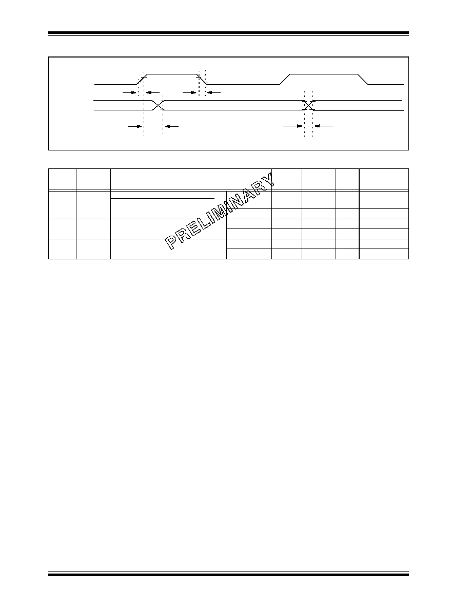
PIC18CXX2
DS39026B-page 268
Preliminary
©
7/99 Microchip Technology Inc.
FIGURE 21-20: USART SYNCHRONOUS TRANSMISSION (MASTER/SLAVE) TIMING
TABLE 21-19: USART SYNCHRONOUS TRANSMISSION REQUIREMENTS
Param.
No.
Symbol
Characteristic
Min
Max
Units
Conditions
120
TckH2dtV SYNC XMIT (MASTER & SLAVE)
Clock high to data out valid
PIC18CXXX
--
40
ns
PIC18LCXXX
--
100
ns
121
Tckrf
Clock out rise time and fall time
(Master Mode)
PIC18CXXX
--
20
ns
PIC18LCXXX
--
50
ns
122
Tdtrf
Data out rise time and fall time
PIC18CXXX
--
20
ns
PIC18LCXXX
--
50
ns
Note: Refer to Figure 21-4 for load conditions.
121
121
120
122
RC6/TX/CK
RC7/RX/DT
pin
pin
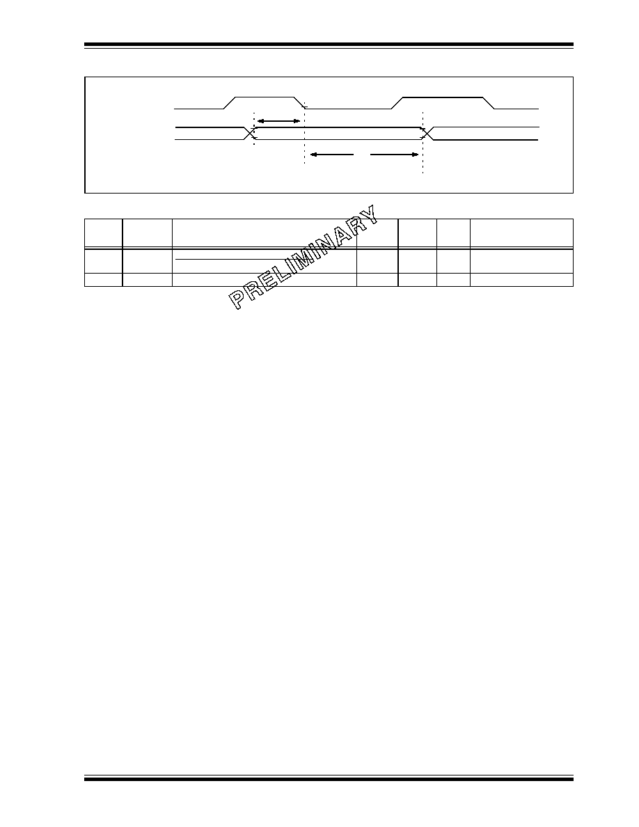
PIC18CXX2
©
7/99 Microchip Technology Inc.
Preliminary
DS39026B-page 269
FIGURE 21-21: USART SYNCHRONOUS RECEIVE (MASTER/SLAVE) TIMING
TABLE 21-20: USART SYNCHRONOUS RECEIVE REQUIREMENTS
Param.
No.
Symbol
Characteristic
Min
Max
Units
Conditions
125
TdtV2ckl
SYNC RCV (MASTER & SLAVE)
Data hold before CK
(DT hold time)
10
--
ns
126
TckL2dtl
Data hold after CK
(DT hold time)
15
--
ns
Note: Refer to Figure 21-4 for load conditions.
125
126
RC6/TX/CK
RC7/RX/DT
pin
pin

PIC18CXX2
DS39026B-page 270
Preliminary
©
7/99 Microchip Technology Inc.
TABLE 21-21: A/D CONVERTER CHARACTERISTICS:
PIC18CXX2 (INDUSTRIAL, EXTENDED)
PIC18LCXX2 (INDUSTRIAL)
Param
No.
Symbol Characteristic
Min
Typ
Max
Units Conditions
A01
N
R
Resolution
--
--
--
--
10
TBD
bit
bit
V
REF
= V
DD
3.0V
V
REF
= V
DD
<
3.0V
A03
E
IL
Integral linearity error
--
--
--
--
<±1
TBD
LSb
LSb
V
REF
= V
DD
3.0V
V
REF
= V
DD
<
3.0V
A04
E
DL
Differential linearity error
--
--
--
--
<±1
TBD
LSb
LSb
V
REF
= V
DD
3.0V
V
REF
= V
DD
<
3.0V
A05
E
FS
Full scale error
--
--
--
--
<±1
TBD
LSb
LSb
V
REF
= V
DD
3.0V
V
REF
= V
DD
<
3.0V
A06
E
OFF
Offset error
--
--
--
--
<±1
TBD
LSb
LSb
V
REF
= V
DD
3.0V
V
REF
= V
DD
<
3.0V
A10
--
Monotonicity
guaranteed
(3)
--
V
SS
V
AIN
V
REF
A20
V
REF
Reference voltage
(V
REFH
- V
REFL
)
0V
--
--
V
A20A
3V
--
--
V
For 10-bit resolution
A21
V
REFH
Reference voltage High
AV
SS
--
AV
DD
+ 0.3V
V
A22
V
REFL
Reference voltage Low
AV
SS
- 0.3V
--
AV
DD
V
A25
V
AIN
Analog input voltage
AV
SS
- 0.3V
--
V
REF
+ 0.3V
V
A30
Z
AIN
Recommended impedance of
analog voltage source
--
--
10.0
k
A40
I
AD
A/D conversion
current (V
DD
)
PIC18CXXX
--
180
--
µ
A
Average current
consumption when
A/D is on. (Note 1)
PIC18LCXXX
--
90
--
µ
A
A50
I
REF
V
REF
input current (Note 2)
10
--
--
--
1000
10
µ
A
µ
A
During V
AIN
acquisition.
Based on differential of
V
HOLD
to V
AIN
. To charge
C
HOLD
see Section 16.0.
During A/D conversion
cycle
Note 1: When A/D is off, it will not consume any current other than minor leakage current. The power-down current
spec includes any such leakage from the A/D module.
V
REF
current is from RA2/AN2/V
REF
- and RA3/AN3/V
REF
+ pins or AV
DD
and AV
SS
pins, whichever is
selected as reference input.
2: V
SS
V
AIN
V
REF
3: The A/D conversion result either increases or remains constant as the analog input increases.
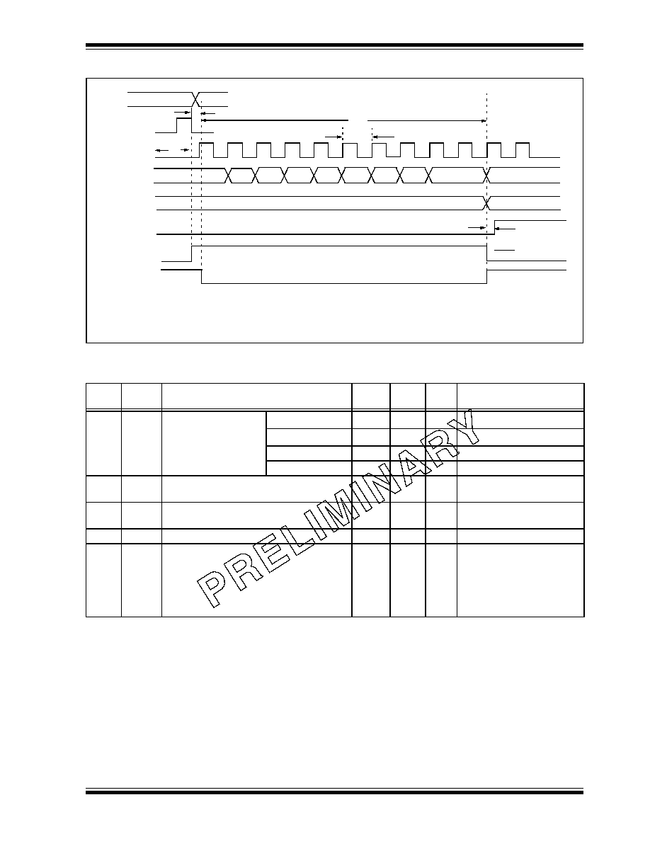
PIC18CXX2
©
7/99 Microchip Technology Inc.
Preliminary
DS39026B-page 271
FIGURE 21-22: A/D CONVERSION TIMING
TABLE 21-22: A/D CONVERSION REQUIREMENTS
Param
No.
Symbol
Characteristic
Min
Max
Units
Conditions
130
T
AD
A/D clock period
PIC18CXXX
1.6
20
(5)
µ
s
T
OSC
based, V
REF
3.0V
PIC18LCXXX
3.0
20
(5)
µ
s
T
OSC
based, V
REF
full range
PIC18CXXX
2.0
6.0
µ
s
A/D RC Mode
PIC18LCXXX
3.0
9.0
µ
s
A/D RC Mode
131
T
CNV
Conversion time
(not including acquisition time) (Note 1)
11
12
T
AD
132
T
ACQ
Acquisition time (Note 3)
15
10
--
--
µ
s
µ
s
-40
∞
C
Temp
125
∞
C
0
∞
C
Temp
125
∞
C
135
T
SWC
Switching Time from convert
sample
--
Note 4
136
T
AMP
Amplifier settling time (Note 2)
1
--
µ
s
This may be used if the
"new" input voltage has not
changed by more than 1LSb
(i.e. 5 mV @ 5.12V) from the
last sampled voltage (as
stated on C
HOLD
).
Note 1: ADRES register may be read on the following T
CY
cycle.
2: See the Section 16.0 for minimum conditions, when input voltage has changed more than 1 LSb.
3: The time for the holding capacitor to acquire the "New" input voltage, when the voltage changes full scale
after the conversion (AV
DD
to AV
SS
, or AV
SS
to AV
DD
). The source impedance (
R
S
) on the input channels is
50
.
4: On the next Q4 cycle of the device clock.
5: The time of the A/D clock period is dependent on the device frequency and the T
AD
clock divider.
131
130
132
BSF ADCON0, GO
Q4
A/D CLK
A/D DATA
ADRES
ADIF
GO
SAMPLE
OLD_DATA
SAMPLING STOPPED
DONE
NEW_DATA
Note 2
9
8
7
2
1
0
Note 1: If the A/D clock source is selected as RC, a time of T
CY
is added before the A/D clock starts.
This allows the
SLEEP
instruction to be executed.
2: This is a minimal RC delay (typically 100 nS), which also disconnects the holding capacitor from the
analog input.
. . .
. . .
T
CY

PIC18CXX2
DS39026B-page 272
Preliminary
©
7/99 Microchip Technology Inc.
NOTES:

PIC18CXX2
©
7/99 Microchip Technology Inc.
Preliminary
DS39026B-page 273
22.0
DC AND AC
CHARACTERISTICS GRAPHS
AND TABLES
Graphs and Tables not available at this time.

PIC18CXX2
DS39026B-page 274
Preliminary
©
7/99 Microchip Technology Inc.
NOTES:

PIC18CXX2
©
7/99 Microchip Technology Inc.
Preliminary
DS39026B-page 275
23.0
PACKAGING INFORMATION
23.1
Package Marking Information
Not available at time of printing. Will be made available
after definition of QS9000 compliant standard
23.2
Package Details
The following sections give the technical details of the
packages.
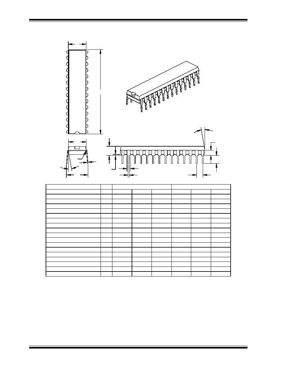
PIC18CXX2
DS39026B-page 276
Preliminary
©
7/99 Microchip Technology Inc.
Package Type:
28-Lead Skinny Plastic Dual In-line (SP) ≠ 300 mil
*
Controlling Parameter.
Dimension "B1" does not include dam-bar protrusions. Dam-bar protrusions shall not exceed 0.003"
(0.076 mm) per side or 0.006" (0.152 mm) more than dimension "B1."
Dimensions "D" and "E" do not include mold flash or protrusions. Mold flash or protrusions shall not
exceed 0.010" (0.254 mm) per side or 0.020" (0.508 mm) more than dimensions "D" or "E."
JEDEC equivalent: MO-095 AH
0.320
0.270
0.280
1.345
0.125
0.015
0.070
0.140
0.008
0.000
0.040
0.016
Mold Draft Angle Bottom
Mold Draft Angle Top
Overall Row Spacing
Radius to Radius Width
Molded Package Width
Tip to Seating Plane
Base to Seating Plane
Top of Lead to Seating Plane
Top to Seating Plane
Upper Lead Width
Lower Lead Width
PCB Row Spacing
Package Length
Lead Thickness
Shoulder Radius
Number of Pins
Dimension Limits
Pitch
Units
E
eB
E1
A1
A2
L
D
A
c
R
n
B1
B
p
MIN
MIN
0.295
0.288
5
5
10
0.350
0.283
10
0.380
0.295
15
15
0.090
1.365
0.130
0.020
0.150
0.010
0.005
NOM
INCHES*
28
0.053
0.019
0.100
0.300
1.385
0.135
0.025
0.110
0.160
0.012
0.010
0.065
0.022
MAX
7.49
7.30
7.11
8.89
7.18
5
8.13
6.86
5
10
10
15
15
9.65
7.49
34.67
3.30
0.51
2.29
3.81
0.25
0.13
1.33
0.48
2.54
7.62
MILLIMETERS
1.78
34.16
3.18
0.38
3.56
0.20
0.00
1.02
0.41
NOM
2.79
35.18
3.43
0.64
4.06
0.30
0.25
MAX
28
1.65
0.56
n
1
2
R
D
E
c
eB
E1
p
L
A1
B
B1
A
A2
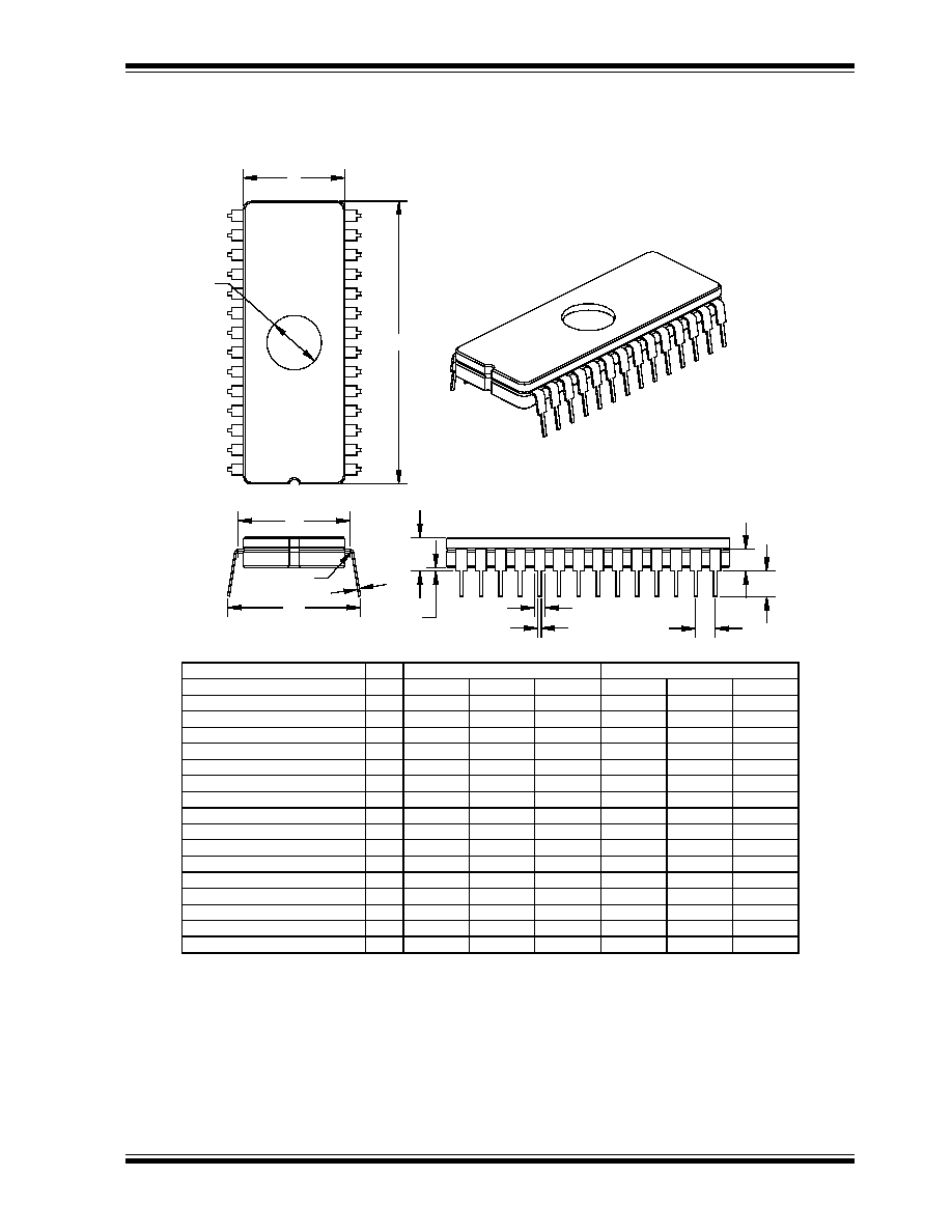
PIC18CXX2
©
7/99 Microchip Technology Inc.
Preliminary
DS39026B-page 277
Package Type:
28-Lead Ceramic Dual In-line with Window (JW) ≠ 600 mil
* Controlling Parameter.
JEDEC equivalent:
MO-103 AB
n
1
2
R
MIN
Window Diameter
Overall Row Spacing
Radius to Radius Width
Package Width
Package Length
Tip to Seating Plane
Base to Seating Plane
Top of Lead to Seating Plane
Top to Seating Plane
Lead Thickness
Shoulder Radius
Upper Lead Width
Lower Lead Width
Number of Pins
PCB Row Spacing
Dimension Limits
Units
Pitch
W
eB
E1
A2
D
E
L
A
A1
c
R
B1
B
p
n
7.37
1.40
3.70
5.08
0.30
0.25
1.65
0.53
2.59
0.280
0.660
0.580
0.520
1.460
0.138
0.035
0.128
0.185
0.010
0.270
0.610
0.560
0.015
0.514
1.430
0.125
0.110
0.170
0.008
0.290
0.710
0.600
0.055
0.526
1.490
0.150
0.146
0.200
0.012
0.005
0.058
0.019
0.100
0.600
INCHES*
0.098
0.000
0.050
0.016
NOM
MAX
28
0.102
0.010
0.065
0.021
37.08
6.86
15.49
14.22
13.06
36.32
3.18
0.38
2.78
4.32
0.20
7.11
16.76
14.73
18.03
15.24
0.89
3.49
13.21
3.24
4.70
0.25
13.36
37.85
3.81
NOM
MILLIMETERS
0.00
1.27
0.41
2.49
MIN
2.54
0.13
1.46
0.47
28
15.24
MAX
D
E
W
c
E1
eB
p
A1
L
B1
B
A2
A
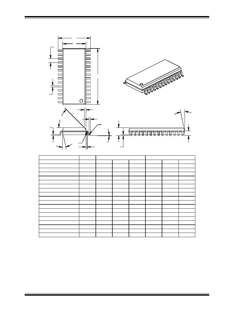
PIC18CXX2
DS39026B-page 278
Preliminary
©
7/99 Microchip Technology Inc.
Package Type:
28-Lead Plastic Small Outline (SO) ≠ Wide, 300 mil
MIN
p
Pitch
Mold Draft Angle Bottom
Mold Draft Angle Top
Lower Lead Width
Radius Centerline
Gull Wing Radius
Shoulder Radius
Chamfer Distance
Outside Dimension
Molded Package Width
Molded Package Length
Shoulder Height
Overall Pack. Height
Lead Thickness
Foot Angle
Foot Length
Standoff
Number of Pins
B
c
X
A2
A1
A
n
E1
L
L1
R1
R2
E
D
Dimension Limits
Units
1.27
0.050
8
12
12
0.017
0
0.014
0
0.019
15
15
0.011
0.015
0.016
0.005
0.005
0.020
0.407
0.296
0.706
0.008
0.058
0.099
28
0.394
0.011
0.009
0.010
0
0.005
0.005
0.010
0.292
0.700
0.004
0.048
0.093
0.419
0.012
0.020
0.021
0.010
0.010
0.029
4
8
0.299
0.712
0.011
0.068
0.104
0.36
0
0
12
12
0.42
15
15
0.48
10.33
17.93
10.01
0.23
0.25
0.28
0.13
0.13
0.25
0
7.42
0.10
1.22
2.36
17.78
10.64
0.41
4
0.27
0.38
0.13
0.13
0.50
0.53
0.30
0.51
0.25
0.25
0.74
7.51
0.19
28
2.50
1.47
18.08
7.59
0.28
2.64
1.73
NOM
INCHES*
MAX
NOM
MILLIMETERS
MIN
MAX
n
1
2
R1
R2
D
p
B
E1
E
L1
L
c
45 ∞
X
A1
A
A2
*
Controlling Parameter.
Dimension "B" does not include dam-bar protrusions. Dam-bar protrusions shall not exceed 0.003"
(0.076 mm) per side or 0.006" (0.152 mm) more than dimension "B."
Dimensions "D" and "E" do not include mold flash or protrusions. Mold flash or protrusions shall not
exceed 0.010" (0.254 mm) per side or 0.020" (0.508 mm) more than dimensions "D" or "E."
JEDEC equivalent: MS-013 AE
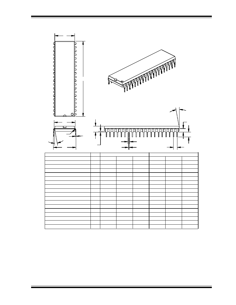
PIC18CXX2
©
7/99 Microchip Technology Inc.
Preliminary
DS39026B-page 279
Package Type:
40-Lead Plastic Dual In-line (P) ≠ 600 mil
*
Controlling Parameter.
Dimension "B1" does not include dam-bar protrusions. Dam-bar protrusions shall not exceed 0.003"
(0.076 mm) per side or 0.006" (0.152 mm) more than dimension "B1."
Dimensions "D" and "E" do not include mold flash or protrusions. Mold flash or protrusions shall not
exceed 0.010" (0.254 mm) per side or 0.020" (0.508 mm) more than dimensions "D" or "E."
JEDEC equivalent: MS-011 AC
n
2
1
R
Top to Seating Plane
Mold Draft Angle Bottom
Mold Draft Angle Top
Overall Row Spacing
Radius to Radius Width
Molded Package Width
Tip to Seating Plane
Base to Seating Plane
Top of Lead to Seating Plane
Package Length
E1
eB
L
E
D
A2
A1
0.670
0.585
0.540
2.023
0.135
0.040
0.113
0.545
5
5
0.630
0.125
0.530
2.013
0.020
0.073
0.565
10
0.610
10
0.130
0.535
2.018
0.020
0.093
16.00
13.84
13.46
51.13
3.18
0.51
1.85
15
15
14.35
5
5
10
15.49
10
3.30
13.59
51.26
0.51
2.36
14.86
17.02
15
15
13.72
51.38
3.43
1.02
2.87
PCB Row Spacing
Lead Thickness
Shoulder Radius
Upper Lead Width
Lower Lead Width
Pitch
Number of Pins
Dimension Limits
Units
p
c
A
R
B
B1
n
0.160
0.011
0.010
0.055
0.020
NOM
INCHES*
0.110
0.009
0.000
0.045
0.016
MIN
0.100
0.160
0.010
0.005
0.050
0.018
40
0.600
MAX
2.79
0.23
0.00
1.14
0.41
MIN
2.54
4.06
0.25
0.13
1.27
0.46
NOM
MILLIMETERS
15.24
40
4.06
0.28
0.25
1.40
0.51
MAX
A1
D
E
c
eB
E1
p
L
B
B1
A
A2
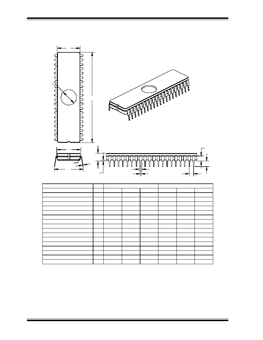
PIC18CXX2
DS39026B-page 280
Preliminary
©
7/99 Microchip Technology Inc.
Package Type:
40-Lead Ceramic Dual In-line with Window (JW) ≠ 600 mil
*
Controlling Parameter.
JEDEC equivalent:
MO-103 AC
n
1
2
R
Window Diameter
Overall Row Spacing
Radius to Radius Width
Package Width
Package Length
Tip to Seating Plane
Base to Seating Plane
Top of Lead to Seating Plane
Top to Seating Plane
Lead Thickness
Shoulder Radius
Upper Lead Width
Lower Lead Width
Number of Pins
PCB Row Spacing
Dimension Limits
Pitch
E1
W
eB
D
E
L
A2
A1
A
c
p
B1
R
B
n
9.14
18.03
15.24
13.36
52.32
3.68
3.89
5.59
0.36
0.25
0.58
2.59
MAX
0.014
0.011
0.008
0.350
0.660
0.580
0.520
2.050
0.140
0.035
0.135
0.205
0.560
0.340
0.610
0.514
2.040
0.135
0.015
0.117
0.190
0.600
0.360
0.710
0.526
2.060
0.145
0.055
0.153
0.220
0.005
0.053
0.020
0.100
0.600
NOM
0.000
0.050
0.016
0.098
MIN
40
0.102
0.010
0.055
0.023
MAX
0.28
0.20
14.22
15.49
8.64
13.06
51.82
3.43
0.38
2.97
4.83
14.73
16.76
8.89
13.21
52.07
3.56
0.89
3.43
5.21
MIN
2.49
1.27
0.00
0.41
2.54
1.33
0.13
0.50
15.24
NOM
40
1.40
1.40
D
W
E
c
eB
E1
p
L
A1
B1
B
A
A2
Units
INCHES*
MILLIMETERS
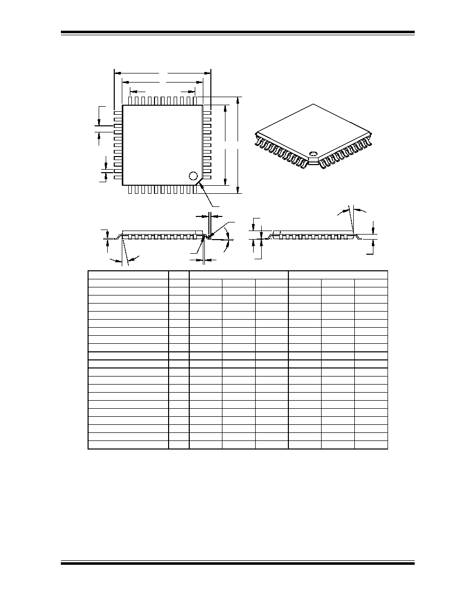
PIC18CXX2
©
7/99 Microchip Technology Inc.
Preliminary
DS39026B-page 281
Package Type:
44-Lead Plastic Thin Quad Flatpack (PT)
10x10x1 mm Body, 1.0/0.1 mm Lead Form
0.025
0.390
0.390
0.463
0.463
0.012
0.004
0.003
0.005
0.003
0.003
0.002
0.015
0.039
p
Mold Draft Angle Bottom
Mold Draft Angle Top
Pin 1 Corner Chamfer
Molded Pack. Width
Molded Pack. Length
Outside Tip Width
Outside Tip Length
Lower Lead Width
Lead Thickness
Radius Centerline
Gull Wing Radius
Shoulder Radius
Shoulder Height
Overall Pack. Height
Pins along Width
Number of Pins
Foot Length
Foot Angle
Standoff
D
X
E
L
D1
E1
B
c
L1
A1
R1
R2
A2
n1
A
n
Dimension Limits
Pitch
Units
MIN
0.398
0.394
5
5
12
0.035
0.394
10
0.045
0.398
15
15
0.010
0
0.472
0.472
0.015
0.006
0.008
3.5
0.025
0.006
0.003
0.004
0.043
11
44
0.015
0.482
0.482
0.018
0.008
0.013
7
0.008
0.010
0.006
0.035
0.047
10.10
10.00
9.90
12
10
0.89
10.00
5
0.64
9.90
5
15
15
1.14
10.10
12.00
12.00
0.38
0.15
0.20
3.5
0.25
0.14
0.08
0.10
0.64
1.10
11
44
0.13
11.75
11.75
0.30
0.09
0.08
0
0.38
0.08
0.08
0.05
1.00
0.38
12.25
12.25
0.45
0.20
0.33
7
0.89
0.20
0.25
0.15
1.20
MIN
NOM
INCHES
0.031
MAX
0.80
MILLIMETERS*
NOM
MAX
X x 45∞
n
1
2
R2
R1
L1
L
c
D1
D
B
p
# leads = n1
E
E1
A1
A2
A
*
Controlling Parameter.
Dimension "B" does not include dam-bar protrusions. Dam-bar protrusions shall not exceed 0.003"
(0.076 mm) per side or 0.006" (0.152 mm) more than dimension "B."
Dimensions "D" and "E" do not include mold flash or protrusions. Mold flash or protrusions shall not
exceed 0.010" (0.254 mm) per side or 0.020" (0.508 mm) more than dimensions "D" or "E."
JEDEC equivalent: MS-026 ACB
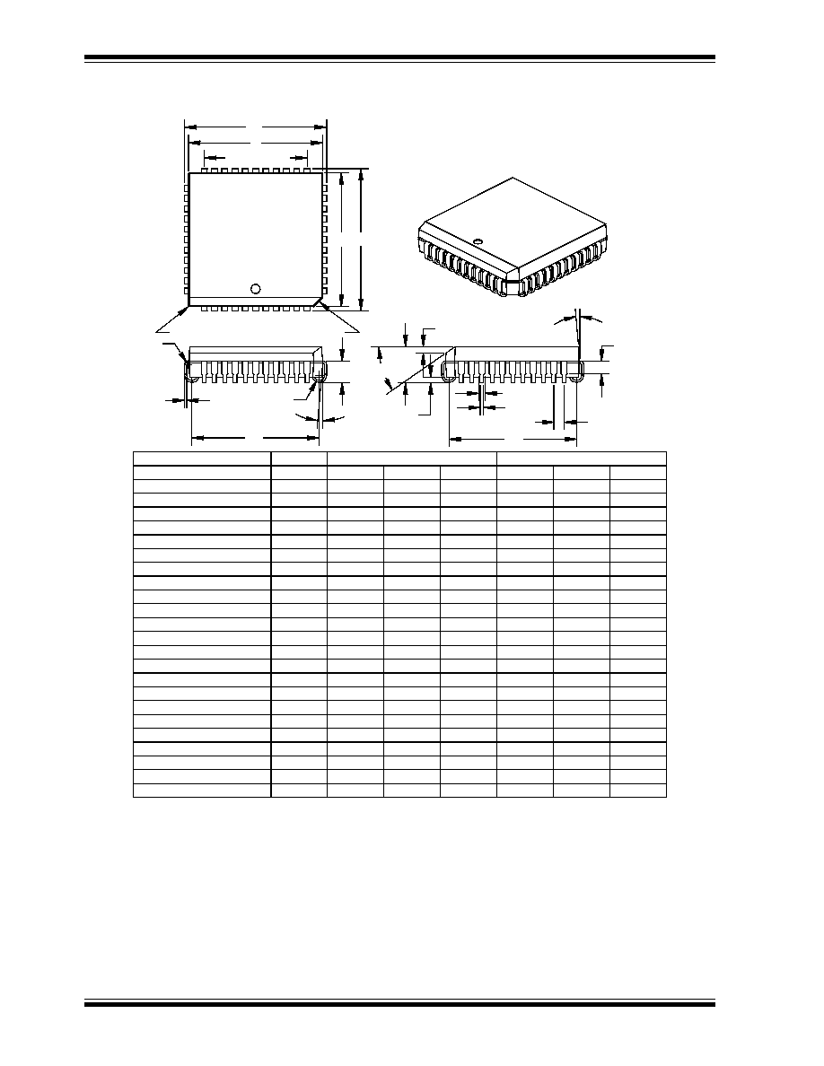
PIC18CXX2
DS39026B-page 282
Preliminary
©
7/99 Microchip Technology Inc.
Package Type:
44-Lead Plastic Leaded Chip Carrier (L) ≠ Square
*
Controlling Parameter.
Dimension "B1" does not include dam-bar protrusions. Dam-bar protrusions shall not exceed 0.003"
(0.076 mm) per side or 0.006" (0.152 mm) more than dimension "B1."
Dimensions "D" and "E" do not include mold flash or protrusions. Mold flash or protrusions shall not
exceed 0.010" (0.254 mm) per side or 0.020" (0.508 mm) more than dimensions "D" or "E."
JEDEC equivalent: MO-047 AC
0.015
0.003
0.050
0.015
0.026
0.008
0.610
0.610
0.650
0.650
0.685
0.685
0.000
0.040
0.024
0.015
0.095
0.165
MIN
p
Pitch
Mold Draft Angle Bottom
Mold Draft Angle Top
J-Bend Inside Radius
Shoulder Inside Radius
Upper Lead Length
Lower Lead Width
Upper Lead Width
Lead Thickness
Pins along Width
Footprint Length
Footprint Width
Molded Pack. Length
Molded Pack. Width
Overall Pack. Length
Overall Pack. Width
Corner Chamfer (other)
Corner Chamfer (1)
Side 1 Chamfer Dim.
Shoulder Height
Overall Pack. Height
Standoff
R2
R1
L
B
B1
D2
E2
CH2
CH1
A3
A2
E1
c
n1
E
D
D1
A1
A
Number of Pins
Dimension Limits
Units
n
1.27
0.050
0
0
0.005
0.025
5
5
0.058
0.018
0.029
0.035
0.010
0.065
0.021
0.032
10
10
0.690
0.620
0.010
0.620
11
0.653
0.653
0.690
0.005
0.045
0.029
0.023
0.103
0.173
0.695
0.012
0.630
0.630
0.656
0.656
0.695
0.010
0.050
0.034
0.030
0.110
0.180
0.64
0.13
1.46
0.46
0.74
0.08
0.38
0
0
1.27
0.38
0.66
5
5
0.25
0.89
10
10
1.65
0.53
0.81
0.25
15.75
15.75
16.59
16.59
17.53
17.53
0.13
1.14
0.74
0.57
2.60
4.38
17.40
15.49
0.20
15.49
16.51
16.51
17.40
0.00
1.02
0.61
0.38
2.41
4.19
17.65
11
16.00
0.30
16.00
16.66
16.66
17.65
0.25
1.27
0.86
0.76
2.79
4.57
INCHES*
NOM
44
MAX
MILLIMETERS
MIN
NOM
MAX
44
1
CH2 x 45∞
n
CH1 x 45∞
2
R2
A1
R1
c
E2
D1
D
# leads = n1
E1
E
p
L
A3
A2
A
35∞
B1
B
D2
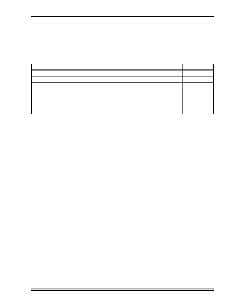
PIC18CXX2
©
7/99 Microchip Technology Inc.
Preliminary
DS39026B-page 283
APPENDIX A: REVISION HISTORY
Revision A
This is a new data sheet.
APPENDIX B: DEVICE DIFFERENCES
The differences between the devices listed in this data
sheet are shown in Table 23-1.
TABLE 23-1:
Device Differences
Feature
PIC18C242
PIC18C252
PIC18C442
PIC18C452
Program Memory (Bytes)
8K
16K
8K
16K
Data Memory (Bytes)
16K
32K
16K
32K
A/D Channels
5
5
8
8
Parallel Slave Port (PSP)
No
No
Yes
Yes
Package Types
28-pin DIP
28-pin SOIC
28-pin JW
28-pin DIP
28-pin SOIC
28-pin JW
40-pin DIP
40-pin PLCC
40-pin TQFP
40-pin JW
40-pin DIP
40-pin PLCC
40-pin TQFP
40-pin JW

PIC18CXX2
DS39026B-page 284
Preliminary
©
7/99 Microchip Technology Inc.
APPENDIX C: CONVERSION
CONSIDERATIONS
This appendix discusses the considerations for con-
verting from previous version of a device to the ones
listed in this data sheet. Typically these changes are
due to the differences in the process technology used.
An example of this type of conversion is from a
PIC16C74A to a PIC16C74B.
Not Applicable
APPENDIX D: MIGRATION FROM
BASELINE TO
ENHANCED DEVICES
This section discusses how to migrate from a Baseline
device (i.e., PIC16C5X) to an Enhanced MCU device
(i.e., PIC18CXXX).
The following are the list of modifications over the
PIC16C5X microcontroller family:
Not Currently Available

PIC18CXX2
©
7/99 Microchip Technology Inc.
Preliminary
DS39026B-page 285
APPENDIX E: MIGRATION FROM
MIDRANGE TO
ENHANCED DEVICES
This section discusses how to migrate from a Midrange
device (i.e., PIC16CXXX) to an Enhanced device (i.e.,
PIC18CXXX).
The following are the list of modifications over the
PIC16CXXX microcontroller family:
Not Currently Available
APPENDIX F: MIGRATION FROM
HIGH-END TO
ENHANCED DEVICES
This section discusses how to migrate from a High-end
device (i.e., PIC17CXXX) to an Enhance MCU device
(i.e., PIC18CXXX).
The following are the list of modifications over the
PIC17CXXX microcontroller family:
Not Currently Available

PIC18CXX2
DS39026B-page 286
Preliminary
©
7/99 Microchip Technology Inc.
NOTES:

©
7/99 Microchip Technology Inc.
Preliminary
DS39026B-page 287
PIC18CXX2
INDEX
A
A/D ................................................................................... 167
A/D Converter Flag (ADIF Bit) ................................. 169
A/D Converter Interrupt, Configuring ....................... 170
ADCON0 Register .................................................... 167
ADCON1 Register ............................................ 167, 168
ADRES Register .............................................. 167, 169
Analog Port Pins .................................................. 89, 90
Analog Port Pins, Configuring .................................. 171
Block Diagram .......................................................... 169
Block Diagram, Analog Input Model ......................... 170
Configuring the Module ............................................ 170
Conversion Clock (T
AD
) ........................................... 171
Conversion Status (GO/DONE Bit) .......................... 169
Conversions ............................................................. 172
Converter Characteristics ........................................ 270
converter characteristics .......................................... 249
Effects of a Reset ..................................................... 179
Operation During Sleep ........................................... 179
Sampling Requirements ........................................... 170
Special Event Trigger (CCP) ............................ 112, 172
Timing Diagram ........................................................ 271
Absolute Maximum Ratings ............................................. 241
ADCON0 Register ............................................................ 167
GO/DONE Bit ........................................................... 169
ADCON1 Register .................................................... 167, 168
ADDLW ............................................................................ 197
ADDWF ............................................................................ 197
ADDWFC ......................................................................... 198
ADRES Register ...................................................... 167, 169
AKS .................................................................................. 139
Analog-to-Digital Converter.
See
A/D
ANDLW ............................................................................ 198
ANDWF ............................................................................ 199
Assembler
MPASM Assembler .................................................. 235
B
Baud Rate Generator ....................................................... 136
BCF .................................................................................. 200
BF .................................................................................... 139
Block Diagrams
Baud Rate Generator ............................................... 136
SSP (SPI Mode) ....................................................... 121
Timer1 ...................................................................... 106
BRG ................................................................................. 136
Brown-out Reset (BOR) ............................................. 24, 181
Timing Diagram ........................................................ 256
BSF .......................... 199, 200, 201, 202, 203, 205, 206, 221
BTFSC ............................................................................. 204
BTFSS ............................................................................. 204
BTG .................................................................................. 205
Bus Collision During a RESTART Condition .................... 148
Bus Collision During a Start Condition ............................. 146
Bus Collision During a Stop Condition ............................. 149
C
C ........................................................................................ 54
CALL ................................................................................ 206
Capture (CCP Module) .................................................... 111
Block Diagram .......................................................... 111
CCP Pin Configuration ............................................. 111
CCPR1H:CCPR1L Registers ................................... 111
Changing Between Capture Prescalers ................... 111
Software Interrupt .................................................... 111
Timer1 Mode Selection ............................................ 111
Capture/Compare/PWM (CCP) ....................................... 109
CCP1 ....................................................................... 110
CCPR1H Register ........................................... 110
CCPR1L Register ............................................ 110
CCP2 ....................................................................... 110
CCPR2H Register ........................................... 110
CCPR2L Register ............................................ 110
Interaction of Two CCP Modules ............................. 110
Timer Resources ..................................................... 110
Timing Diagram ....................................................... 258
Clocking Scheme ............................................................... 37
CLRF ....................................................................... 207, 225
CLRWDT ......................................................................... 207
Code Examples
Loading the SSPBUF register ................................. 122
Code Protection ....................................................... 181, 189
COMF .............................................................................. 208
Compare (CCP Module) .................................................. 112
Block Diagram ......................................................... 112
CCP Pin Configuration ............................................ 112
CCPR1H:CCPR1L Registers .................................. 112
Software Interrupt .................................................... 112
Special Event Trigger ........................ 99, 107, 112, 172
Timer1 Mode Selection ............................................ 112
Configuration Bits ............................................................ 181
Conversion Considerations .............................................. 286
CPFSEQ .......................................................................... 208
CPFSGT .......................................................................... 209
CPFSLT ........................................................................... 209
D
Data Memory ..................................................................... 40
General Purpose Registers ....................................... 40
Special Function Registers ........................................ 40
DAW ................................................................................ 210
DC ..................................................................................... 54
DC Characteristics ................................... 243, 244, 247, 248
DECF ............................................................................... 210
DECFSNZ ........................................................................ 211
DECFSZ .......................................................................... 211
Development Support ...................................................... 235
Device Differences ........................................................... 285
Direct Addressing .............................................................. 49
E
Electrical Characteristics ................................................. 241
Errata ................................................................................... 4
F
Firmware Instructions ...................................................... 191
FS0 .................................................................................... 54
FS1 .................................................................................... 54
FS2 .................................................................................... 54
FS3 .................................................................................... 54
G
General Call Address Sequence ..................................... 133
General Call Address Support ......................................... 133
GOTO .............................................................................. 212
I
I/O Ports ............................................................................ 77
I
2
C (SSP Module) ............................................................ 128
ACK Pulse ....................................................... 129, 130
Addressing ............................................................... 129

PIC18CXX2
DS39026B-page 288
Preliminary
©
7/99 Microchip Technology Inc.
Block Diagram .......................................................... 128
Read/Write Bit Information (R/W Bit) ............... 129, 130
Reception ................................................................. 130
Serial Clock (RC3/SCK/SCL) ................................... 130
Slave Mode .............................................................. 129
Timing Diagram, Data .............................................. 265
Timing Diagram, Start/Stop Bits ............................... 264
Transmission ............................................................ 130
I
2
C Master Mode Reception ............................................. 139
I
2
C Master Mode Restart Condition ................................. 138
I
2
C Module
Acknowledge Sequence timing ................................ 142
Baud Rate Generator ............................................... 136
BRG Block Diagram ................................................. 136
BRG Reset due to SDA Collision ............................. 147
BRG Timing ............................................................. 136
Bus Collision
Acknowledge .................................................... 145
Restart Condition ............................................. 148
Restart Condition Timing (Case1) .................... 148
Restart Condition Timing (Case2) .................... 148
Start Condition ................................................. 146
Start Condition Timing ............................. 146, 147
Stop Condition ................................................. 149
Stop Condition Timing (Case1) ........................ 149
Stop Condition Timing (Case2) ........................ 149
Transmit Timing ............................................... 145
Bus Collision timing .................................................. 145
Clock Arbitration ....................................................... 144
Clock Arbitration Timing (Master Transmit) .............. 144
General Call Address Support ................................. 133
Master Mode 7-bit Reception timing ........................ 141
Master Mode Operation ........................................... 135
Master Mode Start Condition ................................... 137
Master Mode Transmission ...................................... 139
Master Mode Transmit Sequence ............................ 135
Multi-master Mode ................................................... 145
Repeat Start Condition timing .................................. 138
Stop Condition Receive or Transmit timing .............. 143
Stop Condition timing ............................................... 142
Waveforms for 7-bit Reception ................................ 130
Waveforms for 7-bit Transmission ........................... 130
ID Locations ............................................................. 181, 189
INCF ................................................................................. 212
INCFSNZ .......................................................................... 213
INCFSZ ............................................................................ 213
In-Circuit Serial Programming (ICSP) ...................... 181, 189
Indirect Addressing ............................................................ 49
FSR Register ............................................................. 48
Instruction Cycle ................................................................. 37
Instruction Flow/Pipelining ................................................. 38
Instruction Format ............................................................ 193
Instruction Set .................................................................. 191
ADDLW .................................................................... 197
ADDWF .................................................................... 197
ADDWFC ................................................................. 198
ANDLW .................................................................... 198
ANDWF .................................................................... 199
BCF .......................................................................... 200
BSF .................. 199, 200, 201, 202, 203, 205, 206, 221
BTFSC ..................................................................... 204
BTFSS ..................................................................... 204
BTG .......................................................................... 205
CALL ........................................................................ 206
CLRF ................................................................ 207, 225
CLRWDT .................................................................. 207
COMF ...................................................................... 208
CPFSEQ .................................................................. 208
CPFSGT .................................................................. 209
CPFSLT ................................................................... 209
DAW ........................................................................ 210
DECF ....................................................................... 210
DECFSNZ ................................................................ 211
DECFSZ .................................................................. 211
GOTO ...................................................................... 212
INCF ........................................................................ 212
INCFSNZ ................................................................. 213
INCFSZ .................................................................... 213
IORLW ..................................................................... 214
IORWF ..................................................................... 214
MOVFP .................................................................... 216
MOVLB .................................................................... 215
MOVLR ............................................................ 215, 216
MOVLW ................................................................... 217
MOVWF ................................................................... 217
MULLW .................................................................... 218
MULWF .................................................................... 218
NEGW ..................................................................... 219
NOP ......................................................................... 219
RETFIE ............................................................ 221, 222
RETLW .................................................................... 222
RETURN .................................................................. 223
RLCF ....................................................................... 223
RLNCF ..................................................................... 224
RRCF ....................................................................... 224
RRNCF .................................................................... 225
SLEEP ..................................................................... 226
SUBLW .................................................................... 227
SUBWF .................................................... 226, 227, 228
SUBWFB ................................................................. 229
SWAPF .................................................................... 230
TABLRD .................................................................. 231
TABLWT .................................................................. 232
TSTFSZ ................................................................... 233
XORLW ................................................................... 233
XORWF ................................................................... 234
Summary Table ....................................................... 194
INTCON Register
RBIF Bit ..................................................................... 80
Interrupt Sources ....................................................... 65, 181
A/D Conversion Complete ....................................... 170
Capture Complete (CCP) ......................................... 111
Compare Complete (CCP) ....................................... 112
Interrupt on Change (RB7:RB4 ) ............................... 80
RB0/INT Pin, External ................................................ 75
SSP Receive/Transmit Complete ............................ 117
TMR0 Overflow .......................................................... 95
TMR1 Overflow .................................... 97, 99, 105, 107
TMR2 to PR2 Match ................................................ 103
TMR2 to PR2 Match (PWM) ............................ 102, 115
USART Receive/Transmit Complete ....................... 151
Interrupts, Enable Bits
CCP1 Enable (CCP1IE Bit) ..................................... 111
Interrupts, Flag Bits
A/D Converter Flag (ADIF Bit) ................................. 169
CCP1 Flag (CCP1IF Bit) .................................. 111, 112
Interrupt on Change (RB7:RB4) Flag (RBIF Bit) ........ 80
IORLW ............................................................................. 214
IORWF ............................................................................. 214
K
KeeLoq
Æ
Evaluation and Programming Tools ................ 238

©
7/99 Microchip Technology Inc.
Preliminary
DS39026B-page 289
PIC18CXX2
M
Memory Organization
Data Memory ............................................................. 40
Program Memory ....................................................... 33
MOVFP ............................................................................ 216
MOVLB ............................................................................ 215
MOVLR .................................................................... 215, 216
MOVLW ........................................................................... 217
MOVWF ........................................................................... 217
MPLAB Integrated Development Environment Software . 235
MULLW ............................................................................ 218
Multi-Master Mode ........................................................... 145
Multiply Examples
16 x 16 Routine .......................................................... 62
16 x 16 Signed Routine .............................................. 63
8 x 8 Routine .............................................................. 62
8 x 8 Signed Routine .................................................. 62
MULWF ............................................................................ 218
N
NEGW .............................................................................. 219
NOP ................................................................................. 219
O
OPCODE Field Descriptions ............................................ 192
OPTION_REG Register ..................................................... 51
PS2:PS0 Bits ............................................................. 95
PSA Bit ....................................................................... 95
T0CS Bit ..................................................................... 95
T0SE Bit ..................................................................... 95
OSCCON ........................................................................... 18
OSCCON Register ............................................................. 18
Oscillator Configuration .............................................. 15, 181
HS .............................................................................. 15
LP ............................................................................... 15
RC ........................................................................ 15, 16
XT .............................................................................. 15
Oscillator, Timer1 ......................................... 97, 99, 105, 107
Oscillator, WDT ................................................................ 185
OV ...................................................................................... 54
P
Packaging ........................................................................ 275
Parallel Slave Port (PSP) ............................................. 85, 90
Block Diagram ............................................................ 90
RE0/RD/AN5 Pin .................................................. 89, 90
RE1/WR/AN6 Pin ................................................. 89, 90
RE2/CS/AN7 Pin .................................................. 89, 90
Read Waveforms ....................................................... 91
Select (PSPMODE Bit) ........................................ 85, 90
Timing Diagram ........................................................ 259
Write Waveforms ....................................................... 90
PICDEM-1 Low-Cost PICmicro Demo Board ................... 237
PICDEM-2 Low-Cost PIC16CXX Demo Board ................ 237
PICDEM-3 Low-Cost PIC16CXXX Demo Board .............. 237
PICSTART
Æ
Plus Entry Level Development System ...... 237
Pin Functions
MCLR/Vpp ............................................................. 8, 11
OSC1/CLKIN .......................................................... 8, 11
OSC2/CLKOUT ...................................................... 8, 11
RA0/AN0 ................................................................ 8, 11
RA1/AN1 ................................................................ 8, 11
RA2/AN2 ................................................................ 8, 11
RA3/AN3/Vref ........................................................ 8, 11
RA4/T0CKI ............................................................. 8, 11
RA5/AN4/SS .......................................................... 8, 11
RB0/INT ................................................................. 9, 12
RB1 ........................................................................ 9, 12
RB2 ........................................................................ 9, 12
RB3 ........................................................................ 9, 12
RB4 ........................................................................ 9, 12
RB5 ........................................................................ 9, 12
RB6 ........................................................................ 9, 12
RB7 ........................................................................ 9, 12
RC0/T1OSO/T1CKI ............................................. 10, 13
RC1/T1OSI/CCP2 ............................................... 10, 13
RC2/CCP1 ........................................................... 10, 13
RC3/SCK/SCL ..................................................... 10, 13
RC4/SDI/SDA ...................................................... 10, 13
RC5/SDO ............................................................. 10, 13
RC6/TX/CK .......................................................... 10, 13
RC7/RX/DT .......................................................... 10, 13
RD0/PSP0 ................................................................. 14
RD1/PSP1 ................................................................. 14
RD2/PSP2 ................................................................. 14
RD3/PSP3 ................................................................. 14
RD4/PSP4 ................................................................. 14
RD5/PSP5 ................................................................. 14
RD6/PSP6 ................................................................. 14
RD7/PSP7 ................................................................. 14
RE0/RD/AN5 ............................................................. 14
RE1/WR/AN6 ............................................................. 14
RE2/CS/AN7 .............................................................. 14
Vdd ...................................................................... 10, 14
Vss ....................................................................... 10, 14
Pointer, FSR ...................................................................... 48
PORTA
Initialization ................................................................ 77
PORTA Register ........................................................ 77
RA3:RA0 and RA5 Port Pins ..................................... 78
RA4/T0CKI Pin .......................................................... 78
TRISA Register .......................................................... 77
PORTB
Initialization ................................................................ 80
PORTB Register ........................................................ 80
RB0/INT Pin, External ............................................... 75
RB3:RB0 Port Pins .................................................... 80
RB7:RB4 Interrupt on Change Flag (RBIF Bit) .......... 80
RB7:RB4 Port Pins .................................................... 80
TRISB Register .......................................................... 80
PORTC
Block Diagram ........................................................... 83
Initialization .................................................... 83, 85, 87
PORTC Register ........................................................ 83
RC3/SCK/SCL Pin ................................................... 130
RC7/RX/DT Pin ....................................................... 153
TRISC Register ................................................. 83, 151
PORTD .............................................................................. 90
Block Diagram ........................................................... 85
Parallel Slave Port (PSP) Function ............................ 85
PORTD Register ........................................................ 85
TRISD Register ......................................................... 85
PORTE
Analog Port Pins .................................................. 89, 90
Block Diagram ........................................................... 87
PORTE Register ........................................................ 87
PSP Mode Select (PSPMODE Bit) ...................... 85, 90
RE0/RD/AN5 Pin ................................................. 89, 90
RE1/WR/AN6 Pin ................................................ 89, 90
RE2/CS/AN7 Pin ................................................. 89, 90
TRISE Register .......................................................... 87
Postscaler, WDT

PIC18CXX2
DS39026B-page 290
Preliminary
©
7/99 Microchip Technology Inc.
Assignment (PSA Bit) ................................................ 95
Rate Select (PS2:PS0 Bits) ....................................... 95
Switching Between Timer0 and WDT ........................ 95
Power-on Reset (POR) .............................................. 24, 181
Oscillator Start-up Timer (OST) ......................... 24, 181
Power-up Timer (PWRT) ................................... 24, 181
Time-out Sequence .................................................... 25
Time-out Sequence on Power-up ........................ 30, 31
Timing Diagram ........................................................ 256
Prescaler, Capture ........................................................... 111
Prescaler, Timer0 ............................................................... 95
Assignment (PSA Bit) ................................................ 95
Rate Select (PS2:PS0 Bits) ....................................... 95
Switching Between Timer0 and WDT ........................ 95
Prescaler, Timer1 ............................................................... 98
Prescaler, Timer2 ............................................................. 115
PRO MATE
Æ
II Universal Programmer ............................ 237
Product Identification System ........................................... 297
Program Counter
PCL Register .............................................................. 37
PCLATH Register ...................................................... 37
Program Memory ............................................................... 33
Interrupt Vector .......................................................... 33
Reset Vector .............................................................. 33
Program Verification ......................................................... 189
Programming, Device Instructions ................................... 191
PWM (CCP Module) ......................................................... 114
Block Diagram .......................................................... 114
CCPR1H:CCPR1L Registers ................................... 115
Duty Cycle ................................................................ 115
Example Frequencies/Resolutions .......................... 116
Output Diagram ........................................................ 114
Period ....................................................................... 115
Set-Up for PWM Operation ...................................... 116
TMR2 to PR2 Match ........................................ 102, 115
Q
Q-Clock ............................................................................ 115
R
RCSTA Register
SPEN Bit .................................................................. 151
Register File ....................................................................... 40
Registers
SSPSTAT ................................................................. 118
T1CON
Diagram ........................................................... 105
Section ............................................................. 105
Reset .......................................................................... 23, 181
Timing Diagram ........................................................ 256
RETFIE .................................................................... 221, 222
RETLW ............................................................................. 222
RETURN .......................................................................... 223
Revision History ............................................................... 285
RLCF ................................................................................ 223
RLNCF ............................................................................. 224
RRCF ............................................................................... 224
RRNCF ............................................................................. 225
S
SCK .................................................................................. 121
SDI ................................................................................... 121
SDO ................................................................................. 121
SEEVAL
Æ
Evaluation and Programming System ............ 238
Serial Clock, SCK ............................................................. 121
Serial Data In, SDI ........................................................... 121
Serial Data Out, SDO ....................................................... 121
Simplified Block Diagram of On-Chip Reset Circuit ........... 23
Slave Select Synchronization .......................................... 125
Slave Select, SS .............................................................. 121
SLEEP ............................................................. 181, 187, 226
Software Simulator (MPLAB-SIM) ................................... 236
Special Features of the CPU ................................... 175, 181
Special Function Registers ................................................ 40
SPI
Master Mode ............................................................ 124
Serial Clock .............................................................. 121
Serial Data In ........................................................... 121
Serial Data Out ........................................................ 121
Slave Select ............................................................. 121
SPI clock .................................................................. 124
SPI Mode ................................................................. 121
SPI Master/Slave Connection .......................................... 123
SPI Module
Master/Slave Connection ......................................... 123
Slave Mode .............................................................. 125
Slave Select Synchronization .................................. 125
Slave Synch Timnig ................................................. 125
Slave Timing with CKE = 0 ...................................... 126
Slave Timing with CKE = 1 ...................................... 126
SS .................................................................................... 121
SSP .................................................................................. 117
Block Diagram (SPI Mode) ...................................... 121
SPI Mode ................................................................. 121
SSPBUF .................................................................. 124
SSPCON1 ............................................................... 119
SSPCON2 ............................................................... 120
SSPSR .................................................................... 124
SSPSTAT ................................................................ 118
TMR2 Output for Clock Shift ............................ 102, 103
SSP Module
SPI Master Mode ..................................................... 124
SPI Master./Slave Connection ................................. 123
SPI Slave Mode ....................................................... 125
SSPCON1 ........................................................................ 119
SSPCON2 ........................................................................ 120
SSPOV ............................................................................ 139
SSPSTAT ........................................................................ 118
SSPSTAT Register
R/W Bit ............................................................ 129, 130
SUBLW ............................................................................ 227
SUBWF ............................................................ 226, 227, 228
SUBWFB ......................................................................... 229
SWAPF ............................................................................ 230
T
TABLRD ........................................................................... 231
TABLWT .......................................................................... 232
Timer Modules
Timer1
Block Diagram ................................................. 106
Timer0 ................................................................................ 93
Clock Source Edge Select (T0SE Bit) ....................... 95
Clock Source Select (T0CS Bit) ................................. 95
Overflow Interrupt ...................................................... 95
Timing Diagram ....................................................... 257
Timer1 ........................................................................ 97, 105
Block Diagram ........................................................... 98
Oscillator .............................................. 97, 99, 105, 107
Overflow Interrupt ................................ 97, 99, 105, 107
Special Event Trigger (CCP) ..................... 99, 107, 112
Timing Diagram ....................................................... 257
TMR1H Register ................................................ 97, 105

©
7/99 Microchip Technology Inc.
Preliminary
DS39026B-page 291
PIC18CXX2
TMR1L Register ................................................. 97, 105
Timer2
Block Diagram .......................................................... 103
Postscaler.
See
Postscaler, Timer2
PR2 Register .................................................... 102, 115
Prescaler.
See
Prescaler, Timer2
SSP Clock Shift ................................................ 102, 103
TMR2 Register ......................................................... 102
TMR2 to PR2 Match Interrupt .................. 102, 103, 115
Timing Diagrams
Acknowledge Sequence Timing ............................... 142
Baud Rate Generator with Clock Arbitration ............ 136
BRG Reset Due to SDA Collision ............................ 147
Bus Collision
Start Condition Timing ..................................... 146
Bus Collision During a Restart Condition (Case 1) .. 148
Bus Collision During a Restart Condition (Case2) ... 148
Bus Collision During a Start Condition (SCL = 0) .... 147
Bus Collision During a Stop Condition ..................... 149
Bus Collision for Transmit and Acknowledge ........... 145
I
2
C Bus Data ............................................................ 267
I
2
C Master Mode First Start bit timing ...................... 137
I
2
C Master Mode Reception timing .......................... 141
I
2
C Master Mode Transmission timing ..................... 140
Master Mode Transmit Clock Arbitration .................. 144
Repeat Start Condition ............................................. 138
Slave Synchronization ............................................. 125
SPI Mode Timing (Master Mode)SPI Mode
Master Mode Timing Diagram ......................... 124
SPI Mode Timing (Slave Mode with CKE = 0) ......... 126
SPI Mode Timing (Slave Mode with CKE = 1) ......... 126
Stop Condition Receive or Transmit ........................ 143
Time-out Sequence on Power-up ........................ 30, 31
USART Asynchronous Master Transmission ........... 158
USART Asynchronous Reception ............................ 160
USART Synchronous Reception .............................. 164
USART Synchronous Transmission ........................ 162
Wake-up from SLEEP via Interrupt .......................... 188
Timing Diagrams and Specifications ................................ 253
A/D Conversion ........................................................ 271
Brown-out Reset (BOR) ........................................... 256
Capture/Compare/PWM (CCP) ................................ 258
CLKOUT and I/O ...................................................... 255
External Clock .......................................................... 253
I
2
C Bus Data ............................................................ 265
I
2
C Bus Start/Stop Bits ............................................. 264
Oscillator Start-up Timer (OST) ............................... 256
Parallel Slave Port (PSP) ......................................... 259
Power-up Timer (PWRT) ......................................... 256
Reset ........................................................................ 256
Timer0 and Timer1 ................................................... 257
USART Synchronous Receive ( Master/Slave) ....... 269
USART SynchronousTransmission ( Master/Slave) 268
Watchdog Timer (WDT) ........................................... 256
TRISE Register .................................................................. 87
PSPMODE Bit ...................................................... 85, 90
TSTFSZ ........................................................................... 233
TXSTA Register
BRGH Bit ................................................................. 153
U
Universal Synchronous Asynchronous Receiver Transmitter.
See
USART
USART ............................................................................. 151
Asynchronous Mode ................................................ 157
Master Transmission ....................................... 158
Receive Block Diagram ................................... 159
Reception ........................................................ 160
Transmit Block Diagram .................................. 157
Baud Rate Generator (BRG) ................................... 153
Baud Rate Error, Calculating ........................... 153
Baud Rate Formula ......................................... 153
Baud Rates, Asynchronous Mode (BRGH=0) . 155
Baud Rates, Asynchronous Mode (BRGH=1) . 156
Baud Rates, Synchronous Mode ..................... 154
High Baud Rate Select (BRGH Bit) ................. 153
Sampling ......................................................... 153
Serial Port Enable (SPEN Bit) ................................. 151
Synchronous Master Mode ...................................... 161
Reception ........................................................ 164
Timing Diagram, Synchronous Receive .......... 269
Timing Diagram, Synchronous Transmission .. 268
Transmission ................................................... 162
Synchronous Slave Mode ........................................ 165
W
Wake-up from SLEEP .............................................. 181, 187
Timing Diagram ....................................................... 188
Watchdog Timer (WDT) ........................................... 181, 185
Block Diagram ......................................................... 186
Programming Considerations .................................. 185
RC Oscillator ........................................................... 185
Time-out Period ....................................................... 185
Timing Diagram ....................................................... 256
Waveform for General Call Address Sequence ............... 133
WCOL .............................................................. 137, 139, 142
WCOL Status Flag ........................................................... 137
WWW, On-Line Support ...................................................... 4
X
XORLW ........................................................................... 233
XORWF ........................................................................... 234
Z
Z ........................................................................................ 54

PIC18CXX2
DS39026B-page 292
Preliminary
©
7/99 Microchip Technology Inc.

©
7/99 Microchip Technology Inc.
Preliminary
DS39026B-page 293
PIC18CXX2
Systems Information and Upgrade Hot Line
The Systems Information and Upgrade Line provides
system users a listing of the latest versions of all of
Microchip's development systems software products.
Plus, this line provides information on how customers
can receive any currently available upgrade kits.The
Hot Line Numbers are:
1- 800-755-2345 for U.S. and most of Canada, and
1- 602-786-7302 for the rest of the world.
Trademarks: The Microchip name, logo, PIC, PICmicro,
PICSTART, PICMASTER and PRO MATE are registered
trademarks of Microchip Technology Incorporated in the
U.S.A. and other countries.
Flex
ROM, MPLAB and
fuzzy-
LAB are trademarks and SQTP is a service mark of Micro-
chip in the U.S.A.
All other trademarks mentioned herein are the property of
their respective companies.
ON-LINE SUPPORT
Microchip provides on-line support on the Microchip
World Wide Web (WWW) site.
The web site is used by Microchip as a means to make
files and information easily available to customers. To
view the site, the user must have access to the Internet
and a web browser, such as Netscape or Microsoft
Explorer. Files are also available for FTP download
from our FTP site.
Connecting to the Microchip Internet Web Site
The Microchip web site is available by using your
favorite Internet browser to attach to:
www.microchip.com
The file transfer site is available by using an FTP ser-
vice to connect to:
ftp://ftp.microchip.com
The web site and file transfer site provide a variety of
services. Users may download files for the latest
Development Tools, Data Sheets, Application Notes,
User's Guides, Articles and Sample Programs. A vari-
ety of Microchip specific business information is also
available, including listings of Microchip sales offices,
distributors and factory representatives. Other data
available for consideration is:
∑ Latest Microchip Press Releases
∑ Technical Support Section with Frequently Asked
Questions
∑ Design Tips
∑ Device Errata
∑ Job Postings
∑ Microchip Consultant Program Member Listing
∑ Links to other useful web sites related to
Microchip Products
∑ Conferences for products, Development Sys-
tems, technical information and more
∑ Listing of seminars and events
981103

PIC18CXX2
DS39026B-page 294
Preliminary
©
7/99 Microchip Technology Inc.
READER RESPONSE
It is our intention to provide you with the best documentation possible to ensure successful use of your Microchip prod-
uct. If you wish to provide your comments on organization, clarity, subject matter, and ways in which our documentation
can better serve you, please FAX your comments to the Technical Publications Manager at (602) 786-7578.
Please list the following information, and use this outline to provide us with your comments about this Data Sheet.
1.
What are the best features of this document?
2.
How does this document meet your hardware and software development needs?
3.
Do you find the organization of this data sheet easy to follow? If not, why?
4.
What additions to the data sheet do you think would enhance the structure and subject?
5.
What deletions from the data sheet could be made without affecting the overall usefulness?
6.
Is there any incorrect or misleading information (what and where)?
7.
How would you improve this document?
8.
How would you improve our software, systems, and silicon products?
To:
Technical Publications Manager
RE:
Reader Response
Total Pages Sent
From: Name
Company
Address
City / State / ZIP / Country
Telephone: (_______) _________ - _________
Application (optional):
Would you like a reply? Y N
Device:
Questions:
FAX: (______) _________ - _________
DS39026B
PIC18CXX2
Literature Number:

©
1999 Microchip Technology Inc.
Preliminary
DS39026B-page 295
PIC18CXX2
PIC18CXX2 PRODUCT IDENTIFICATION SYSTEM
To order or obtain information, e.g., on pricing or delivery, refer to the factory or the listed sales office.
Sales and Support
PART NO.
-
X
/XX
XXX
Pattern
Package
Temperature
Range
Device
Device
PIC18CXX2
(1)
, PIC18CXX2T
(2);
V
DD
range 4.2V to 5.5V
PIC18LCXX2
(1)
, PIC18LCXX2T
(2);
V
DD
range 2.5V to 5.5V
Temperature
Range
I
= -40
∞
C to+85◊C(Industrial)
E
= -40
∞
C to+125◊C(Extended)
Package
JW
=
Windowed CERDIP
(3)
PT
=
TQFP (Thin Quad Flatpack)
SO
=
SOIC
SP
=
Skinny plastic dip
P
=
PDIP
L
=
PLCC
Pattern
QTP, SQTP, Code or Special Requirements
(blank otherwise)
Examples:
a)
PIC18LC452 - I/P 301 = Industrial
temp., PDIP package, 4 MHz,
Extended V
DD
limits, QTP pattern
#301.
b)
PIC18LC242 - I/SO = Industrial
temp., SOIC package, Extended
V
DD
limits.
c)
PIC18C442 - E/P = Extended temp.,
PDIP package, 40MHz, normal V
DD
limits.
Note1: C
= Standard Voltage range
LC = Wide Voltage Range
2:
T
= in tape and reel - SOIC,
PLCC, and TQFP
packages only.
3:
JW Devices are UV erasable and
can be programmed to any device
configuration. JW Devices meet
the electrical requirement of each
oscillator type (including LC
devices).
Data Sheets
Products supported by a preliminary Data Sheet may have an errata sheet describing minor operational differences and recom-
mended workarounds. To determine if an errata sheet exists for a particular device, please contact one of the following:
1.
Your local Microchip sales office
2.
The Microchip Corporate Literature Center U.S. FAX: (602) 786-7277
3.
The Microchip Worldwide Site (www.microchip.com)
Please specify which device, revision of silicon and Data Sheet (include Literature #) you are using.
New Customer Notification System
Register on our web site (www.microchip.com/cn) to receive the most current information on our products.

Information contained in this publication regarding device applications and the like is intended for suggestion only and may be superseded by updates. No representation or warranty is given and no liability is assumed
by Microchip Technology Incorporated with respect to the accuracy or use of such information, or infringement of patents or other intellectual property rights arising from such use or otherwise. Use of Microchip's products
as critical components in life support systems is not authorized except with express written approval by Microchip. No licenses are conveyed, implicitly or otherwise, under any intellectual property rights. The Microchip
logo and name are registered trademarks of Microchip Technology Inc. in the U.S.A. and other countries. All rights reserved. All other trademarks mentioned herein are the property of their respective companies.
1999 Microchip Technology Inc.
All rights reserved. © 1999 Microchip Technology Incorporated. Printed in the USA. 11/99
Printed on recycled paper.
AMERICAS
Corporate Office
Microchip Technology Inc.
2355 West Chandler Blvd.
Chandler, AZ 85224-6199
Tel: 480-786-7200 Fax: 480-786-7277
Technical Support: 480-786-7627
Web Address: http://www.microchip.com
Atlanta
Microchip Technology Inc.
500 Sugar Mill Road, Suite 200B
Atlanta, GA 30350
Tel: 770-640-0034 Fax: 770-640-0307
Boston
Microchip Technology Inc.
5 Mount Royal Avenue
Marlborough, MA 01752
Tel: 508-480-9990 Fax: 508-480-8575
Chicago
Microchip Technology Inc.
333 Pierce Road, Suite 180
Itasca, IL 60143
Tel: 630-285-0071 Fax: 630-285-0075
Dallas
Microchip Technology Inc.
4570 Westgrove Drive, Suite 160
Addison, TX 75248
Tel: 972-818-7423 Fax: 972-818-2924
Dayton
Microchip Technology Inc.
Two Prestige Place, Suite 150
Miamisburg, OH 45342
Tel: 937-291-1654 Fax: 937-291-9175
Detroit
Microchip Technology Inc.
Tri-Atria Office Building
32255 Northwestern Highway, Suite 190
Farmington Hills, MI 48334
Tel: 248-538-2250 Fax: 248-538-2260
Los Angeles
Microchip Technology Inc.
18201 Von Karman, Suite 1090
Irvine, CA 92612
Tel: 949-263-1888 Fax: 949-263-1338
New York
Microchip Technology Inc.
150 Motor Parkway, Suite 202
Hauppauge, NY 11788
Tel: 631-273-5305 Fax: 631-273-5335
San Jose
Microchip Technology Inc.
2107 North First Street, Suite 590
San Jose, CA 95131
Tel: 408-436-7950 Fax: 408-436-7955
AMERICAS
(continued)
Toronto
Microchip Technology Inc.
5925 Airport Road, Suite 200
Mississauga, Ontario L4V 1W1, Canada
Tel: 905-405-6279 Fax: 905-405-6253
ASIA/PACIFIC
Hong Kong
Microchip Asia Pacific
Unit 2101, Tower 2
Metroplaza
223 Hing Fong Road
Kwai Fong, N.T., Hong Kong
Tel: 852-2-401-1200 Fax: 852-2-401-3431
Beijing
Microchip Technology, Beijing
Unit 915, 6 Chaoyangmen Bei Dajie
Dong Erhuan Road, Dongcheng District
New China Hong Kong Manhattan Building
Beijing 100027 PRC
Tel: 86-10-85282100 Fax: 86-10-85282104
India
Microchip Technology Inc.
India Liaison Office
No. 6, Legacy, Convent Road
Bangalore 560 025, India
Tel: 91-80-229-0061 Fax: 91-80-229-0062
Japan
Microchip Technology Intl. Inc.
Benex S-1 6F
3-18-20, Shinyokohama
Kohoku-Ku, Yokohama-shi
Kanagawa 222-0033 Japan
Tel: 81-45-471- 6166 Fax: 81-45-471-6122
Korea
Microchip Technology Korea
168-1, Youngbo Bldg. 3 Floor
Samsung-Dong, Kangnam-Ku
Seoul, Korea
Tel: 82-2-554-7200 Fax: 82-2-558-5934
Shanghai
Microchip Technology
RM 406 Shanghai Golden Bridge Bldg.
2077 Yan'an Road West, Hong Qiao District
Shanghai, PRC 200335
Tel: 86-21-6275-5700 Fax: 86 21-6275-5060
ASIA/PACIFIC
(continued)
Singapore
Microchip Technology Singapore Pte Ltd.
200 Middle Road
#07-02 Prime Centre
Singapore 188980
Tel: 65-334-8870 Fax: 65-334-8850
Taiwan, R.O.C
Microchip Technology Taiwan
10F-1C 207
Tung Hua North Road
Taipei, Taiwan, ROC
Tel: 886-2-2717-7175 Fax: 886-2-2545-0139
EUROPE
United Kingdom
Arizona Microchip Technology Ltd.
505 Eskdale Road
Winnersh Triangle
Wokingham
Berkshire, England RG41 5TU
Tel: 44 118 921 5858 Fax: 44-118 921-5835
Denmark
Microchip Technology Denmark ApS
Regus Business Centre
Lautrup hoj 1-3
Ballerup DK-2750 Denmark
Tel: 45 4420 9895 Fax: 45 4420 9910
France
Arizona Microchip Technology SARL
Parc d'Activite du Moulin de Massy
43 Rue du Saule Trapu
Batiment A - ler Etage
91300 Massy, France
Tel: 33-1-69-53-63-20 Fax: 33-1-69-30-90-79
Germany
Arizona Microchip Technology GmbH
Gustav-Heinemann-Ring 125
D-81739 M¸nchen, Germany
Tel: 49-89-627-144 0 Fax: 49-89-627-144-44
Italy
Arizona Microchip Technology SRL
Centro Direzionale Colleoni
Palazzo Taurus 1 V. Le Colleoni 1
20041 Agrate Brianza
Milan, Italy
Tel: 39-039-65791-1 Fax: 39-039-6899883
11/15/99
W
ORLDWIDE
S
ALES
AND
S
ERVICE
Microchip received QS-9000 quality system
certification for its worldwide headquarters,
design and wafer fabrication facilities in
Chandler and Tempe, Arizona in July 1999. The
Company's quality system processes and
procedures are QS-9000 compliant for its
PICmicro
Æ
8-bit MCUs, K
EE
L
OQ
Æ
code hopping
devices, Serial EEPROMs and microperipheral
products. In addition, Microchip's quality
system for the design and manufacture of
development systems is ISO 9001 certified.