2001 Microchip Technology Inc.
Advance Information
DS39541A-page 1
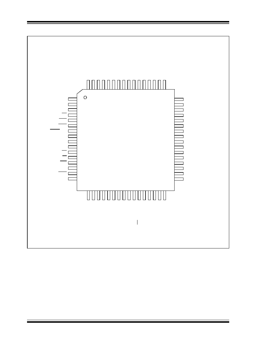
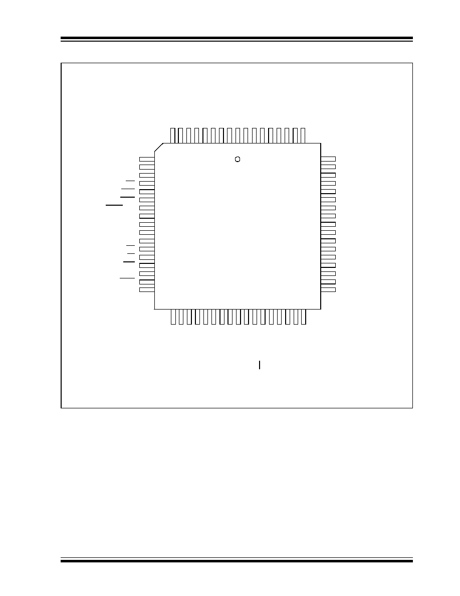
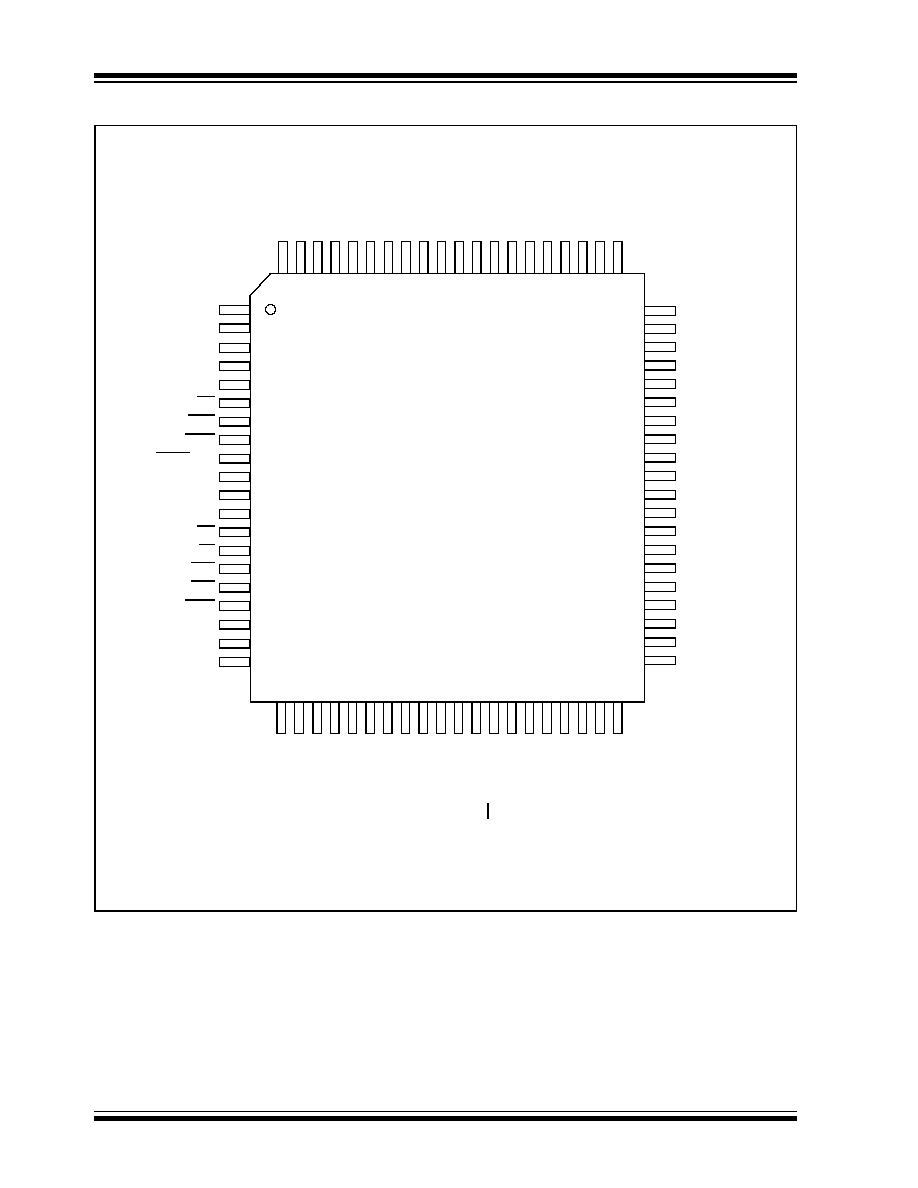
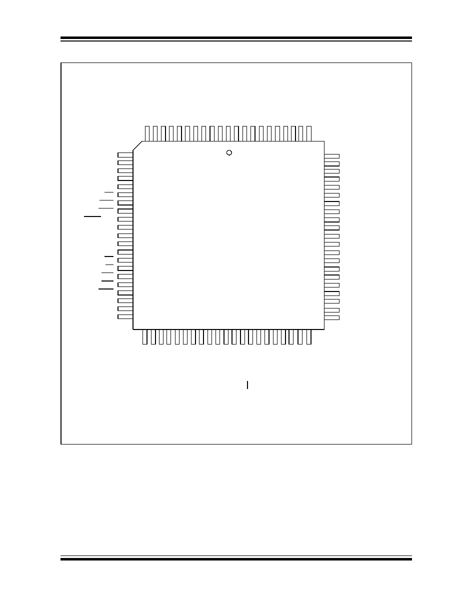
PIC18C601/801
High Performance RISC CPU:
· C compiler optimized architecture instruction set
· Linear program memory addressing up to 2 Mbytes
· Linear data memory addressing to 4 Kbytes
· Up to 160 ns instruction cycle:
- DC - 25 MHz clock input
- 4 MHz - 6 MHz clock input with PLL active
· 16-bit wide instructions, 8-bit wide data path
· Priority levels for interrupts
· 8 x 8 Single Cycle Hardware Multiplier
Peripheral Features:
· High current sink/source 25 mA/25 mA
· Up to 47 I/O pins with individual direction control
· Three external interrupt pins
· Timer0 module: 8-bit/16-bit timer/counter with
8-bit programmable prescaler
· Timer1 module: 16-bit timer/counter (time-base for
CCP)
· Timer2 module: 8-bit timer/counter with 8-bit
period register
· Timer3 module: 16-bit timer/counter
· Secondary oscillator clock option - Timer1/Timer3
· Two Capture/Compare/PWM (CCP) modules
CCP pins can be configured as:
- Capture input: 16-bit, max. resolution 10 ns
- Compare is 16-bit, max. resolution 160 ns (T
CY
)
- PWM output: PWM resolution is 1- to 10-bit
Max. PWM freq. @:
8-bit resolution = 99 kHz
10-bit resolution = 24.4 kHz
· Master Synchronous Serial Port (MSSP) with two
modes of operation:
- 3-wire SPITM (Supports all 4 SPI modes)
- I
2
CTM Master and Slave mode
· Addressable USART module: Supports Interrupt
on Address bit
Advanced Analog Features:
· 10-bit Analog-to-Digital Converter module (A/D)
with:
-
Fast sampling rate
-
Conversion available during SLEEP
-
DNL = ±1 LSb, INL = ±1 LSb
-
Up to 12 channels available
· Programmable Low Voltage Detection (LVD)
module
-
Supports interrupt on Low Voltage Detection
Special Microcontroller Features:
· Power-on Reset (POR), Power-up Timer (PWRT),
and Oscillator Start-up Timer (OST)
· Watchdog Timer (WDT) with its own on-chip RC
oscillator
· On-chip Boot RAM for boot loader application
· 8-bit or 16-bit external memory interface modes
· Up to two software programmable chip select sig-
nals (CS1 and CS2)
· One programmable chip I/O select signal (CSIO)
for memory mapped I/O expansion
· Power saving SLEEP mode
· Different oscillator options, including:
- 4X Phase Lock Loop (of primary oscillator)
- Secondary Oscillator (32 kHz) clock input
CMOS Technology:
· Low power, high speed CMOS technology
· Fully static design
· Wide operating voltage range (2.0V to 5.5V)
· Industrial and Extended temperature ranges
· Low power consumption
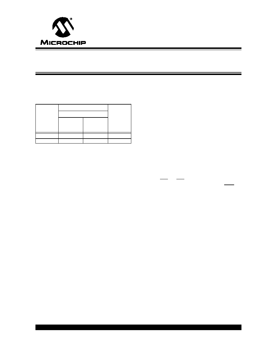
Device
External Program Memory
On-Chip
RAM (bytes)
On-Chip
Maximum
Addressing
(bytes)
Maximum
Single Word
Instructions
PIC18C601
256K
128K
1.5K
PIC18C801
2M
1M
1.5K
High-Performance ROM-less Microcontrollers
with External Memory Bus