2000 Microchip Technology Inc.
Advanced Information
DS30475A-page 1
High Performance RISC CPU:
· C-compiler optimized architecture instruction set
· Linear program memory addressing to 32 Kbytes
· Linear data memory addressing to 4 Kbytes
· Up to 10 MIPS operation:
- DC - 40 MHz clock input
- 4 MHz - 10 MHz osc./clock input with PLL active
· 16-bit wide instructions, 8-bit wide data path
· Priority levels for interrupts
· 8 x 8 Single Cycle Hardware Multiplier
Peripheral Features:
· High current sink/source 25 mA/25 mA
· Up to 76 I/O with individual direction control
· Four external interrupt pins
· Timer0 module: 8-bit/16-bit timer/counter with
8-bit programmable prescaler
· Timer1 module: 16-bit timer/counter
· Timer2 module: 8-bit timer/counter with 8-bit
period register (time base for PWM)
· Timer3 module: 16-bit timer/counter
· Secondary oscillator clock option - Timer1/Timer3
· Two Capture/Compare/PWM (CCP) modules
CCP pins can be configured as:
- Capture input: 16-bit, max resolution 6.25 ns
- Compare is 16-bit, max resolution 100 ns (T
CY
)
- PWM output: PWM resolution is 1- to 10-bit.
Max. PWM freq. @:8-bit resolution = 156 kHz
10-bit resolution = 39 kHz
· Master Synchronous Serial Port (MSSP) with two
modes of operation:
- 3-wire SPITM (Supports all 4 SPI modes)
- I
2
CTM Master and Slave mode
· Addressable USART module: Supports Interrupt
on Address bit
Advanced Analog Features:
· 10-bit Analog-to-Digital Converter module (A/D)
with:
-
Fast sampling rate
-
Conversion available during SLEEP
-
DNL = ±1 LSb, INL = ±1 LSb
-
Up to 16 channels available
· Analog Comparator Module:
-
2 Comparators
-
Programmable input and output multiplexing
· Comparator Voltage Reference Module
· Programmable Low Voltage Detection (LVD)
module
-
Supports interrupt on low voltage detection
· Programmable Brown-out Reset (BOR)
CAN BUS Module Features:
· Message bit rates up to 1 Mbps
· Conforms to CAN 2.0B ACTIVE Spec with:
- 29-bit Identifier Fields
- 8 byte message length
· 3 Transmit Message Buffers with prioritization
· 2 Receive Message Buffers
· 6 full 29-bit Acceptance Filters
· Prioritization of Acceptance Filters
· Multiple Receive Buffers for High Priority
Messages to prevent loss due to overflow
· Advanced Error Management Features
Special Microcontroller Features:
· Power-on Reset (POR), Power-up Timer (PWRT),
and Oscillator Start-up Timer (OST)
· Watchdog Timer (WDT) with its own on-chip RC
oscillator
· Programmable code protection
· Power saving SLEEP mode
· Selectable oscillator options, including:
- 4X Phase Lock Loop (of primary oscillator)
- Secondary Oscillator (32 kHz) clock input
· In-Circuit Serial Programming (ICSPTM) via two pins
CMOS Technology:
· Low power, high speed EPROM technology
· Fully static design
· Wide operating voltage range (2.5V to 5.5V)
· Industrial and Extended temperature ranges
· Low power consumption
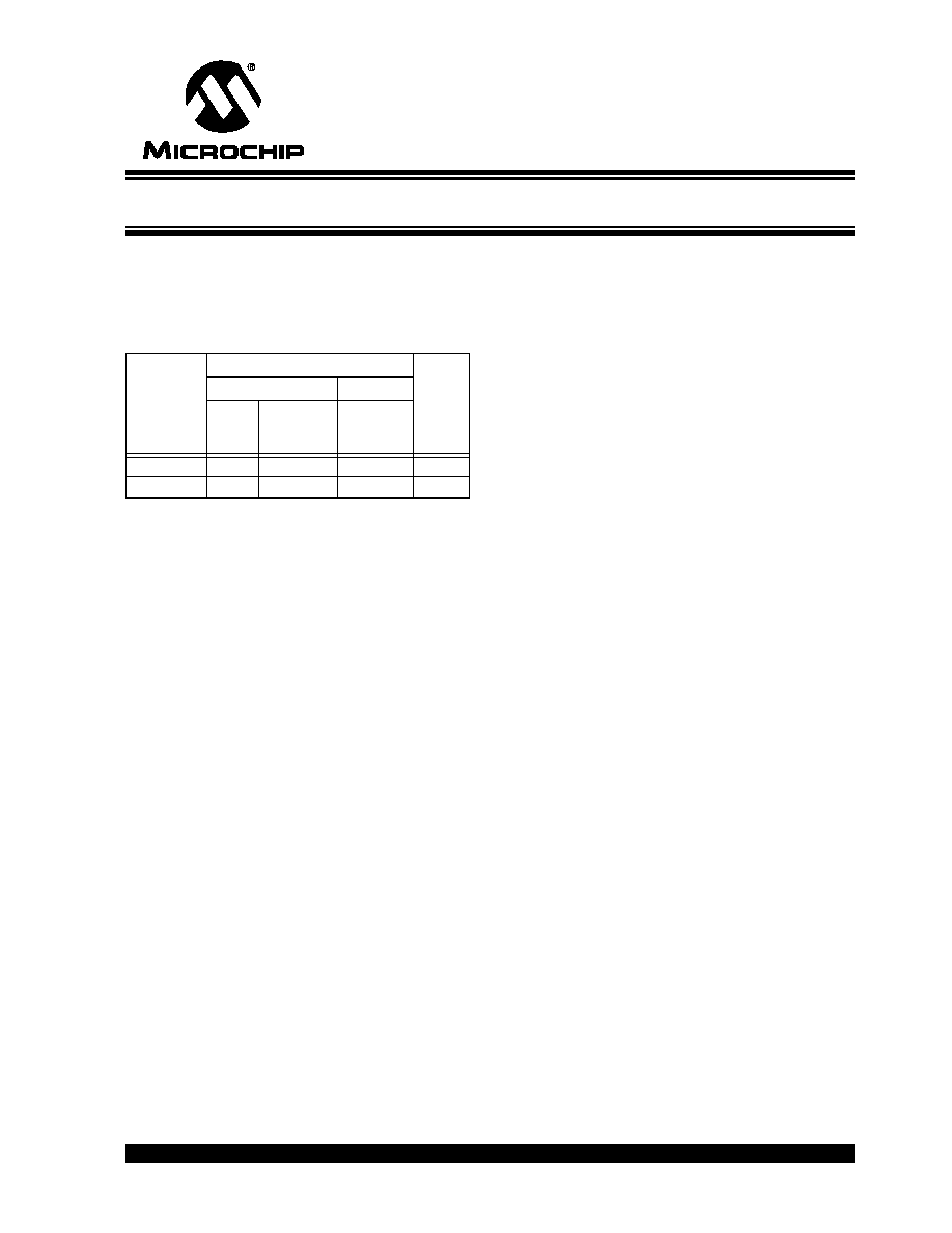
Device
Program Memory
On-Chip
RAM
(bytes)
On-Chip Off-Chip
EPROM
(bytes)
# Single
Word
Instructions
Maximum
Addressing
(bytes)
PIC18C658
32 K
16384
N/A
1536
PIC18C858
32 K
16384
N/A
1536
PIC18CXX8
High-Performance Microcontrollers with CAN Module