 | ÐлекÑÑоннÑй компоненÑ: TC815 | СкаÑаÑÑ:  PDF PDF  ZIP ZIP |
Äîêóìåíòàöèÿ è îïèñàíèÿ www.docs.chipfind.ru
©
2002 Microchip Technology Inc.
DS21474B-page 1
TC815
Features
· Auto-Range Operation for AC and DC Voltage
and Resistance Measurements
- Two User Selected AC/DC Current Ranges
20mA and 200mA
· 22 Operating Ranges
- 9 DC/AC Voltage
- 4 AC/DC Current
- 9 Resistance and Low Power Ohms
· Display HOLD Function
· 3-1/2 Digit Resolution in Auto-Range Mode:
- 1/2000
· Extended Resolution in Manual Mode: 1/3000
· Memory Mode for Relative Measurements:
- ±5% F.S.
· Internal AC to DC Conversion Op Amp
· Triplex LCD Drive for Decimal Points, Digits
and Annunciators
· Continuity Detection and Piezoelectric
Transducer Driver
· Compact Surface Mounted 64-pin
Plastic Flat Package
· Low Drift Internal Reference: 75ppm/°C
· 9V Battery Operation: 10mW
· Low Battery Detection and LCD Annunciator
Device Selection Table
General Description
The TC815 is a 3-1/2 digit integrating analog-to-digital
converter with triplex LCD display drive and automatic
ranging. A display hold function is on-chip. Input volt-
age/ohm attenuators ranging from 1 to 1/10,000 are
automatically selected. Five full scale ranges are pro-
vided. The CMOS TC815 contains all the logic and
analog switches needed to manufacture an auto-
ranging instrument for ohms and voltage measure-
ments. User selected 20mA and 200mA current ranges
are available. Full scale range and decimal point LCD
annunciators are automatically set in auto-range oper-
ation. Auto-range operation is available during ohms
(high and low power ohms) and voltage (AC and DC)
measurements, eliminating expensive range switches
in hand-held DMM designs. The auto-range feature
may be bypassed allowing decimal point selection and
input attenuator selection control through a single line
input. Expensive rotary switches are not required.
During Manual mode operation, resolution is extended
to 3000 counts full scale. The extended range opera-
tion is indicated by a flashing 1 MSD. The extended
resolution is also available during 200k
and 2000V
full scale auto-range operation.
The Memory mode subtracts a reading, up to ±5% of
full scale from subsequent measurements. Typical
applications involve probe resistance compensation for
resistance measurements, tolerance measurements,
and tare weight measurements.
The TC815 includes an AC to DC converter for
AC measurements. Only external diodes/resistors/
capacitors are required.
A complete LCD annunciator set describes the TC815
meter function and measurement range during ohms,
voltage and current operation. AC measurements are
indicated as well as auto-range operation. A low battery
detection circuit also sets the low battery display
annunciator. The triplex LCD display drive levels may
be set and temperature compensation applied via the
V
DISP
pin. With HOLD low, the display is not updated.
A HOLD mode LCD annunciator is activated.
The "low ohms" measurement option allows in-circuit
resistance measurements by preventing semiconduc-
tor junctions from being forward biased.
Part Number
Package
Operating
Temperature Range
TC815CBU
64-Pin PQFP
0
°
C to +70
°
C
3-1/2 Digit Auto-Ranging A/D Converter with
Triplex LCD Drive and Display Hold Function
TC815
DS21474B-page 2
©
2002 Microchip Technology Inc.
A continuity buzzer output is activated with inputs less
than 1% of full scale. An overrange input signal also
enables the buzzer, except during resistance measure-
ments, and flashes the MSD display.
Featuring single 9V battery operation, 10mW power
consumption, a precision internal voltage reference
(75ppm/°C max TC) and a compact surface mounted
64-pin quad flat package, the TC815 is ideal for porta-
ble instruments.
Package Type
47
52
51
50
49
64
63
62
58
57
56
55
54
53
60
59
24
25
26
27
28
29
30
18
19
20
21
22
23
32
17
1
2
3
4
5
6
7
8
9
10
11
12
13
14
15
45
44
43
42
41
40
39
38
37
36
35
34
33
48
TC815
C
REFL
RM
REFH
ANALOG COM
V
CC
AC//AUTO
BCP3
V
SSD
FE2
AGD2
-MEM/BATT
BCP2
FE1
AGD1
BCP1
16
OHM
20mA
BUZ
FE0
AGD0
BCP0
XTAL1
XTAL2
V
DISP
BP1
BP2
BP3
LO
/A
/V
k/m/
HOLD
NC
46
R1
R4
R2
R3
C
I
ACVL
I
I
C
REFH
REFHI
V
I
VR4
VR5
VR2
VR3
R5
NC
61
31
NC
RM
REFL
R
X
CFI
AD1
AD0
R
BUF
RVIBUF
ACVH
V
SSA
DGND
RANGE
-MEM
I
HOLD
C
AZ
NC
DC/AC
/LOW
64-Pin PQFP
©
2002 Microchip Technology Inc.
DS21474B-page 3
TC815
Typical Application and Test Circuit
-MEM
AUTO
HOLD
LO
k
mVA
AC
+
11
50
7
8
9
1
0
12
13
25
31
39
26
24
23
22
21
20
19
18
16
15
14
R6/100k
R7/100k
R8/220
(PTC)
Positive
Temperature
Coefficient
Resistor
R5/1.6385M
38
R4/163.85k
37
R3/16.385k
36
R2/1638.5
35
45
44
41
40
42
53
52
56
46
54
55
49
47
60
51
32
33
29
34
ADI
ACVH
ACVL
R
BUF
RVIBUF
C
AZ
INT
HOLD
CIF
C
REFL
C
REFH
ANALOG
COM
REFHI
30
61
59
62
63
2
3
58
27
57
28
6
RM
REFH
-MEM
Manual RANGE Change
DC/AC or
/LOW
I
OHMS
20mA
Digital GND
V
SSD
V
SSA
V
CC
XTAL1
BUZ
XTAL2
5
4
43
V
I
(
÷
1)
V
R2
(
÷
10)
V
R3
(
÷
100)
V
R4
(
÷
1,000)
V
R5
(
÷
10,000)
ADO
R1/163.85
R14/9.9M
R12/1.11M
R11/101k
R10/10k
R9/1k
R13
500k
Z1
6.2V
20mA
200mA
Current
Input
Voltage
Input
Common
0.01
µF
Ohms
Input
0.1µF
If LCD Bias is Connected to DIG GND,
Peak Drive Signal
5V.
LCD Bias
Tri-Plex
LCD Display
Segment & Decimal Point Drive
1's
10's
100's
1000's
Display
Annunciators
Backplane
Drivers
Ohms Range Attenuator
RMREFL
R5 (
÷
10,000)
R4 (
÷
1,000)
R3 (
÷
100)
R2 (
÷
10)
R1 (
÷
1)
I I
RX
VDISP
BP1
BP2
BP3
LO
/A
V
K/m
HOLD
AC/
/AUTO
-MEM/
BATT
BCP3
BCP2
FE2
AGD2
BCP1
FE1
AGD1
BCP0
FE0
AGD0
R15
9
R16
1
D3
D4
Enable
Audio
Transducer
32.768kHz
( 33kHz)
9V
+
39pf
V
V
20mA
20mA
200mA
200mA
SIB
SIA
To V
CC
153.850mV
R19/5k
R18/24k
C
REF
0.1µF
R20
100
k
C6
0.01µF
C
INT
C
AZ
150
k
200
k
0.1µF
0.1µF
R
BUF
RVIBUF
R26/3k
R24/10k
R23/10k
R22/470k
R21/2.2M
C4/µf
4.7µf
C2/0.22µF
R27/2k
C1/1µF
C5/1µf
+
+
D1
D2
Voltage Range Attenuator
*Not Required when Resistor Network is used.
TC815
3-1/2 Digit Auto-Ranging DMM
with HOLD Function
TC815
DS21474B-page 4
©
2002 Microchip Technology Inc.
1.0
ELECTRICAL
CHARACTERISTICS
Absolute Maximum Ratings*
Supply Voltage (V+ to V) ..................................... 15V
Analog Input Voltage (Either Input) ................ V+ to V-
Reference Input Voltage.................................. V+ to V-
Voltage at Pin 45 ........................................GND ±0.7V
Power Dissipation (T
A
70°C)
64-Pin Plastic Flat Package ...........................1.14W
Operating Temperature Range:
Commercial Package (C) .................... 0°C to +70°C
Storage Temperature Range .............. -65°C to +150°C
*Stresses above those listed under "Absolute Maximum
Ratings" may cause permanent damage to the device. These
are stress ratings only and functional operation of the device
at these or any other conditions above those indicated in the
operation sections of the specifications is not implied.
Exposure to Absolute Maximum Rating conditions for
extended periods may affect device reliability.
TC815 ELECTRICAL SPECIFICATIONS
Electrical Characteristics: V
A
= 9V, T
A
= +25°C, unless otherwise specified (see Typical Application and Test Circuit Figure).
Symbol
Parameter
Min
Typ
Max
Unit
Test Conditions
Zero Input Reading Input Resistor
-0000
0000
+0000
Digital Reading
200mV Range w/o 10M
Input
-0001
--
+0001
Digital Reading
200mV Range w/10M
Input
-0000
0000
+0000
Digital Reading
20mA and 200mA Range
RE
Rollover Error
--
--
±1 Count
200mV Range w/o 10M
Input Resistor
--
--
±3
200mV Range w/10M
Input
--
--
±1
20mA and 200mA Range
NL
Linearity Error
--
--
±1
Count
Best Case Straight Line
I
IN
Input Leakage Current
--
--
10
pA
E
N
Input Noise
--
20
--
µ
V
p-p
BW = 0.1 to 10Hz
AC Frequency Error
--
±1
--
%
40Hz to 500Hz
--
±5
--
%
40Hz to 200Hz
Open Circuit Voltage
--
570
660
mV
Excludes 200
Range
for OHM Measurements
Open Circuit Voltage
--
285
350
mV
Excludes 200
Range
for LO OHM Measurement
V
COM
Analog Common Voltage
2.5
2.6
3.3
V
(V
+
- V
COM
)
V
CTC
Common Voltage Temperature
Coefficient
--
--
50
ppm/°C
Display Multiplex Rate
--
100
--
Hz
V
IL
Low Logic Input
--
--
1
V
20mA, AC, I, LOW
, HOLD
Range, -MEM, OHMs
(Relative to DGND Pin 58)
Logic 1 Pull-up Current
--
25
--
µ
A
20mA, AC, I, LOW
, HOLD
Range, -MEM, OHMs
(Relative to DGND Pin 58)
Buzzer Drive Frequency
--
4
--
kHz
Low Battery Flag Voltage
6.3
6.6
7.0
V
V
CC
to V
SSA
Operating Supply Current
--
0.8
1.5
mA
©
2002 Microchip Technology Inc.
DS21474B-page 5
TC815
2.0
PIN DESCRIPTIONS
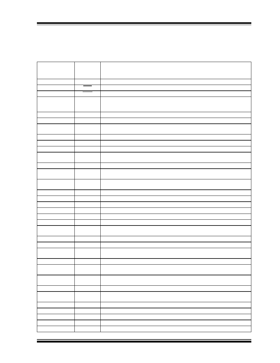
The descriptions of the pins are listed in Table 2-1.
TABLE 2-1:
PIN FUNCTION TABLE
Pin Number
(64-Pin Plastic)
Quad Flat Package
Symbol
Description
1
NC
Logic Input. "0" (Digital Ground) for resistance measurement.
2
OHM
Logic Input. "0" (Digital Ground) for 20mA full scale current measurement.
3
20mA
Audio frequency, 4kHz, output for continuity indication during resistance measurement.
4
BUZ
Audio frequency, 4kHz, output for continuity indication during resistance measurement. A
non-continuous 4kHz signal is output to indicate an input overrange during voltage or
current measurements.
5
XTAL1
32.768kHz Crystal Connection.
6
XTAL2
32.768kHz Crystal Connection.
7
V
DISP
Sets peak LCD drive signal: V
P
- V
DD
- V
DISP
. V
DISP
may also be used to compensate for
temperature variation of LCD crystal threshold voltage.
8
BP1
LCD Backplane #1.
9
BP2
LCD Backplane #2.
10
BP3
LCD Backplane #3.
11
LO
/A
LCD Annunciator segment drive for low ohms resistance measurement and current
measurement.
12
/V
LCD Annunciator segment drive for resistance measurement and voltage measurement.
13
k/m/HOLD
LCD Annunciator segment drive for k ("kilo-ohms"), m ("milliamps" and
"millivolts") and HOLD mode.
14
BCP0
(One's digit)
LCD segment drive for "b," "c" segments and decimal point of least significant digit (LSD).
15
ADG0
LCD segment drive for "a," "g," "d" segments of LSD.
16
FE0
LCD segment drive for "f" and "e" segments of LSD.
17
NC
No connection.
18
BCP1
LCD segment drive for "b," "c" segments and decimal point of 2nd LSD.
19
AGD1
LCD segment drive for "a," "g," "d" segments of 2nd LSD (Ten's digit).
20
FE1
LCD segment drive for "f" and "e" segments of 2nd LSD.
21
BCP2
LCD segment drive for "b," "c" segments and decimal point of 3rd LSD
(Hundred's digit).
22
AGD2
LCD segment drive for "a," "g," "d" segments of 3rd LSD.
23
FE2
LCD segment drive for "b," "c" segments and decimal point of 3rd LSD.
24
BCP3
LCD segment drive for "b," "c" segments and decimal point of MSD
(Thousand's digit).
25
AC/-/AUTO
LCD annunciator drive signal for AC measurements, polarity, and auto-range operation.
26
-MEM/BATT
LCD annunciator drive signal for low battery indication and Memory
(Relative Measurement) mode.
27
V
SSD
Negative battery supply connection for internal digital circuits. Connect to negative terminal
of battery.
28
V
CC
Positive battery supply connection.
29
ANALOG
COM
Analog circuit ground reference point. Nominally 2.6V below V
CC
.
30
RM
REFH
Ratiometric (Resistance measurement) reference high voltage.
31
RM
REFL
Ratiometric (Resistance measurement) reference low voltage.
32
C
REFL
Reference capacitor negative terminal C
REF
0.1µf.
33
C
REFH
Reference capacitor positive terminal C
REF
0.1µf.
34
REFHI
Reference voltage for voltage and current measurement; nominally 163.85mV.