 | –≠–ª–µ–∫—Ç—Ä–æ–Ω–Ω—ã–π –∫–æ–º–ø–æ–Ω–µ–Ω—Ç: TCN75MOA | –°–∫–∞—á–∞—Ç—å:  PDF PDF  ZIP ZIP |

©
2002 Microchip Technology Inc.
DS21490B-page 1
TCN75
Features
∑ Solid-State Temperature Sensing;
0.5∞C Accuracy (Typ.)
∑ Operates from -55∞C to +125∞C
∑ Operating Supply Range: 2.7V to 5.5V
∑ Programmable Trip Point and Hysteresis with
Power-up Defaults
∑ Standard 2-Wire Serial Interface
∑ Thermal Event Alarm Output Functions as
Interrupt or Comparator / Thermostat Output
∑ Up to 8 TCN75s may Share the Same Bus
∑ Shutdown Mode for Low Standby Power
Consumption
∑ 5V Tolerant I/O at V
DD
= 3V
∑ Low Power:
- 250
µ
A (Typ.) Operating
- 1
µ
A (Typ.) Shutdown Mode
∑ 8-Pin SOIC and MSOP Packaging
Applications
∑ Thermal Protection for High Performance CPUs
∑ Solid-State Thermometer
∑ Fire/Heat Alarms
∑ Thermal Management in Electronic Systems:
- Computers
- Telecom Racks
- Power Supplies / UPS/ Amplifiers
∑ Copiers / Office Electronics
∑ Consumer Electronics
∑ Process Control
Package Type
General Description
The TCN75 is a serially programmable temperature
sensor that notifies the host controller when ambient
temperature exceeds a user programmed set point.
Hysteresis is also programmable. The INT/CMPTR
output is programmable as either a simple comparator
for thermostat operation or as a temperature event
interrupt.
Communication
with
the
TCN75
is
accomplished via a two-wire bus that is compatible with
industry standard protocols. This permits reading the
current temperature, programming the set point and
hysteresis, and configuring the device.
The TCN75 powers up in Comparator mode with a
default set point of 80∞C with 5∞C hysteresis. Defaults
allow
independent
operation
as
a
stand-alone
thermostat. A shutdown command may be sent via the
2-wire bus to activate the low power Standby mode.
Address selection inputs allow up to eight TCN75s to
share the same 2-wire bus for multizone monitoring.
All registers can be read by the host and the INT/
CMPTR output's polarity is user programmable. Both
polled
and
interrupt
driven
systems
are
easily
accommodated. Small physical size, low installed cost,
and ease of use make the TCN75 an ideal choice for
implementing
sophisticated
system
management
schemes.
1
2
3
4
8
7
6
5
TCN75MOA
1
2
3
4
8
7
6
5
TCN75MUA
A1
A0
A2
SOIC
MSOP
SCL
INT/CMPTR
GND
SDA
SCL
INT/CMPTR
GND
SDA
V
DD
A1
A0
A2
V
DD
2-Wire Serial Temperature Sensor and Thermal Monitor

TCN75
DS21490B-page 2
©
2002 Microchip Technology Inc.
Device Selection Table
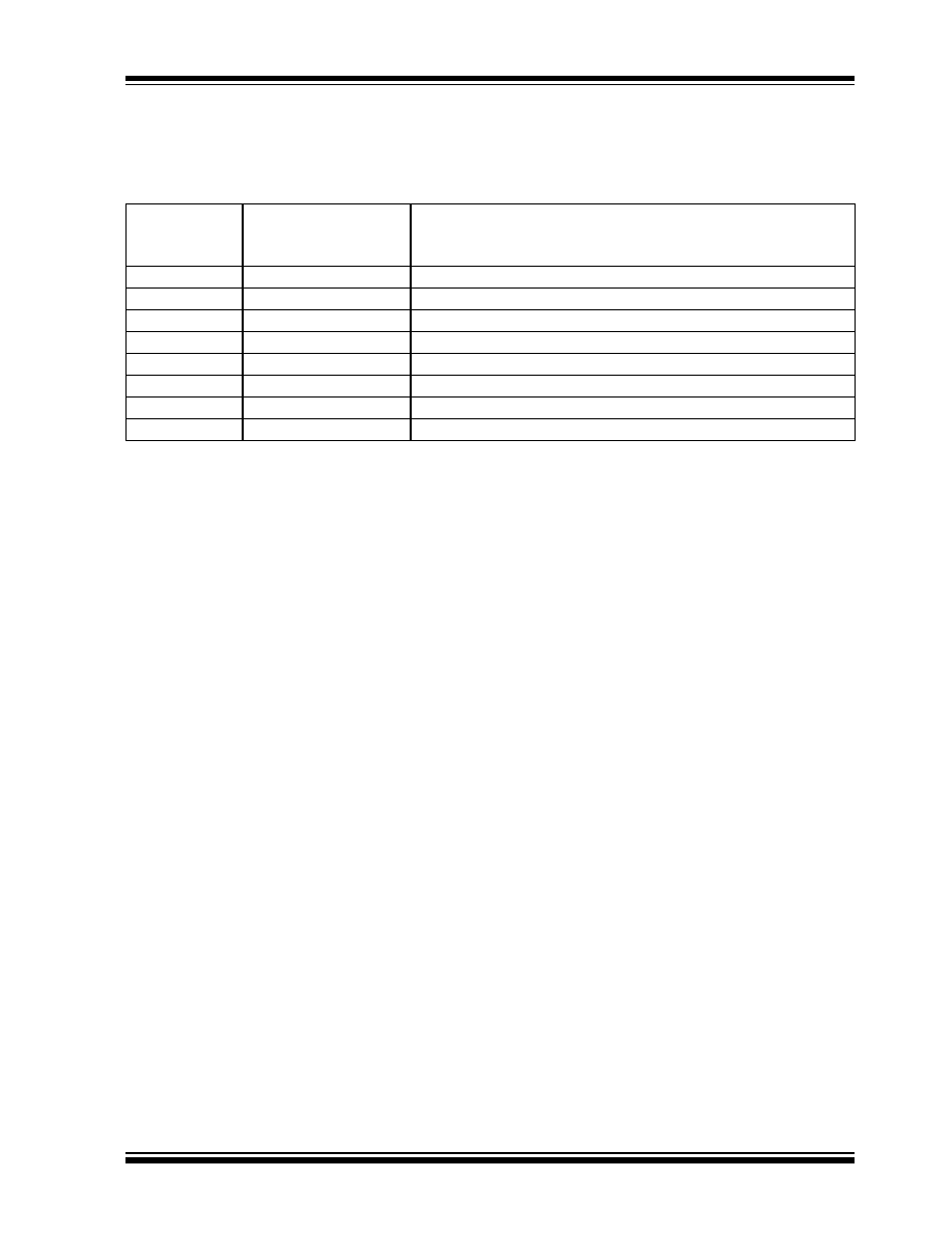
Functional Block Diagram
Part Number
Supply Voltage
Package
Junction Temperature Range
TCN75-3.3MOA
3.3
8-Pin SOIC
-55∞C to +125∞C
TCN75-5.0MOA
5.0
8-Pin SOIC
-55∞C to +125∞C
TCN75-3.3MUA
3.3
8-Pin MSOP
-55∞C to +125∞C
TCN75-5.0MUA
5.0
8-PIn MSOP
-55∞C to +125∞C
Control
Logic
TCN75
INT/CMPTR
Register Set
TSET
THYST
Configuration
A0
V
DD
Temp
Sensor
SCL
SDA
A1
A2
Temperature
9-Bit
A/D
Converter
Two Wire
Serial Port
Interface

©
2002 Microchip Technology Inc.
DS21490B-page 3
TCN75
1.0
ELECTRICAL
CHARACTERISTICS
Absolute Maximum Ratings*
Supply Voltage (V
DD
) ............................................ 6.0V
ESD Susceptibility (Note 3) ............................... 1000V
Voltage on Pins:
A0, A1, A2 .......... (GND ≠ 0.3V) to (V
DD
+ 0.3V)
Voltage on Pins:
SDA, SCL, INT/CMPTR .. (GND ≠ 0.3V) to 5.5V
Thermal Resistance (Junction to Ambient)
8-Pin SOIC.......................................... 170∞C/W
8-Pin MSOP ....................................... 250∞C//W
Operating Temperature Range (T
J
): -55∞C to +125∞C
Storage Temperature Range (T
STG
): -65∞C to +150∞C
*Stresses above those listed under "Absolute Maximum Rat-
ings" may cause permanent damage to the device. These are
stress ratings only and functional operation of the device at
these or any other conditions above those indicated in the
operation sections of the specifications is not implied. Expo-
sure to Absolute Maximum Rating conditions for extended
periods may affect device reliability.
TCN75 ELECTRICAL SPECIFICATIONS
Electrical Characteristics: V
DD
= 2.7V ≠ 5.5V, -55∞C
(T
A
= T
J
)
125∞C, unless otherwise noted.
Symbol
Parameter
Min
Typ
Max
Units
Test Conditions
Power Supply
V
DD
Power Supply Voltage
2.7
--
5.5
--
I
DD
Operating Current
--
--
0.250
--
--
1.0
mA
Serial Port Inactive (T
A
= T
J
= 25∞C)
Serial Port Active
I
DD1
Standby Supply Current
--
1
--
µ
A
Shutdown Mode, Serial Port
Inactive (T
A
= T
J
= 25∞C)
INT/CMPTR Output
I
OL
Sink Current: INT/CMPTR,
SDA Outputs
--
1
4
mA
Note 1
t
TRIP
INT/CMPTR Response Time
1
--
6
t
CONV
User Programmable
V
OL
Output Low Voltage
--
--
0.8
V
I
OL
= 4.0mA
Temp-to-Bits Converter
T
Temperature Accuracy (Note 2)
--
±3
--
∞
C
-55∞C
T
A
+125∞C
V
DD
= 3.3V: TCN75-3.3MOA,
TCN75-3.3MUA
V
DD
= 5.0V: TCN75-5.0MOA,
TCN75-5.0MUA
--
±0.5
±3
∞
C
25∞C
T
A
100∞C
t
CONV
Conversion Time
--
55
--
msec
T
SET(PU)
TEMP Default Value
--
80
--
∞
C
Power-up
T
HYST(PU)
T
HYST
Default Value
--
75
--
∞
C
Power-up
2-Wire Serial Bus Interface
V
IH
Logic Input High
V
DD
x 0.7
--
--
V
V
IL
Logic Input Low
--
--
V
DD
x 0.3
V
V
OL
Logic Output Low
--
--
0.4
V
I
OL
= 3mA
C
IN
Input Capacitance SDA, SCL
--
15
--
pF
I
LEAK
I/O Leakage
--
±100
--
pA
(T
A
= T
J
= 25∞C)
I
OL(SDA)
SDA Output Low Current
--
--
6
mA
TCN75
DS21490B-page 4
©
2002 Microchip Technology Inc.
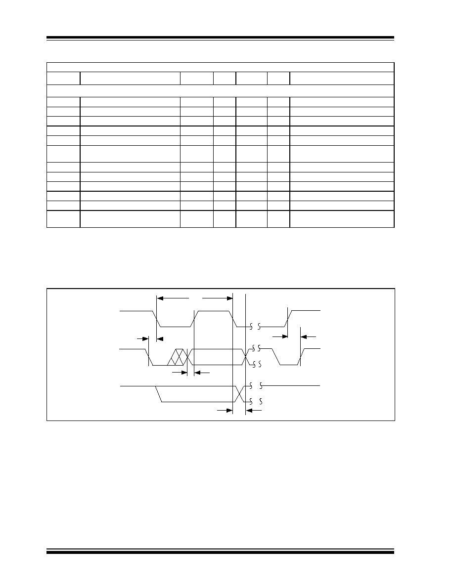
TIMING DIAGRAM
TCN75 ELECTRICAL SPECIFICATIONS (CONTINUED)
Electrical Characteristics: 2.7V
V
DD
5.5V; -55∞C
(T
A
= T
J
)
125∞C, C
L
= 80pF, unless otherwise noted.
Symbol
Parameter
Min
Typ
Max
Unit
Test Conditions
Serial Port Timing
f
SC
Serial Port Frequency
0
100
400
kHz
t
LOW
Low Clock Period
1250
--
--
nsec
t
HIGH
High Clock Period
1250
--
--
nsec
t
R
SCL and SDA Rise Time
--
--
250
nsec
t
F
SCL and SDA Fall Time
--
--
250
nsec
t
SU(START)
START Condition Setup Time (for
repeated START Condition)
1250
--
--
nsec
t
SC
SCL Clock Period
2.5
--
--
µ
sec
t
H(START)
START Condition Hold Time
100
--
--
nsec
t
DSU
Data in Setup Time to SCL High
100
--
--
nsec
t
DH
Data in Hold Time after SCL Low
0
--
--
nsec
t
SU(STOP)
STOP Condition Setup Time
100
--
--
nsec
t
IDLE
Bus Free Time Prior to New Transi-
tion
1250
--
--
nsec
Note
1:
Output current should be minimized for best temperature accuracy. Power dissipation within the TCN75 will cause self-heating and
temperature drift. At maximum rated output current and saturation voltage, 4mA and 0.8V, respectively, the error amounts to 0.544∞C for
the SOIC.
2:
All part types of the TCN75 will operate properly over the wider power supply range of 2.7V to 5.5V. Each part type is tested and specified
for rated accuracy at its nominal supply voltage. As V
DD
varies from the nominal value, accuracy will degrade 1∞C/V of V
DD
change.
3:
Human body model, 100pF discharged through a 1.5k resistor.
SCL
tSC
tDSU
t
SU
(STOP)
t
H
(START)
t
DH
SDA
Data In
SDA
Data Out
©
2002 Microchip Technology Inc.
DS21490B-page 5
TCN75
2.0
PIN DESCRIPTIONS
The descriptions of the pins are listed in Table 2-1.
TABLE 2-1:
PIN FUNCTION TABLE
Pin Number
(8-Pin SOIC)
8-Pin MSOP)
Symbol
Description
1
SDA
Bi-directional Serial Data.
2
SCL
Serial Data Clock Input.
3
INT/CMPTR
Interrupt or Comparator Output.
4
GND
System Ground.
5
A
2
Address Select Pin (MSB).
6
A
1
Address Select Pin.
7
A
0
Address Select Pin (LSB).
8
V
DD
Power Supply Input