HSMBJSAC5.0 thru HSMBJSAC50
500 WATT LOW CAPACITANCE
TRANSIENT VOLTAGE SUPPRESSOR
S C O T T S D A L E D I V I S I O N
W
W
W
.
Mi
c
r
o
s
e
m
i
.
C
O
M
HSMBJSAC5.0 thru
H
S
M
B
JS
A
C50
DESCRIPTION
APPEARANCE
The HSMBJSAC t
ransient voltage suppressor (TVS) series rated at 500
Watts provides an added rectifier element as shown in Figure 4 to achieve
low capacitance in applications for data or signal lines. The low capacitance
rating of less than 30 pF may be used for protecting higher frequency
applications in inductive switching environments or electrical systems
involving secondary lightning effects per IEC61000-4-5 as well as
RTCA/DO-160D or ARINC 429 for airborne avionics. If bidirectional
protection is needed, two HSMBJSAC devices in anti-parallel configuration
are required as shown in Figure 6. With their very fast response time, they
also provide ESD and EFT protection per IEC61000-4-2 and IEC61000-4-4
respectively.
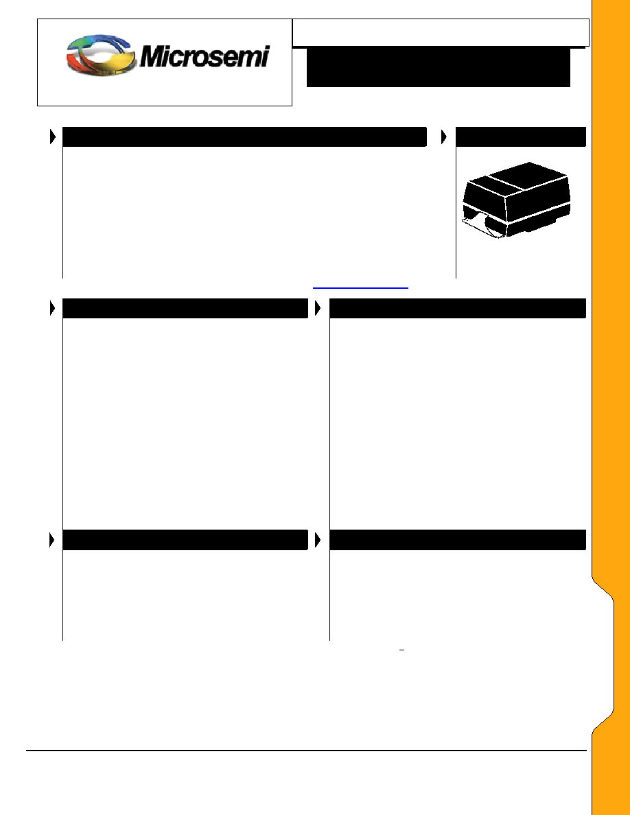
DO-214AA
See package notes
IMPORTANT: For the most current data, consult MICROSEMI's website:
http://www.microsemi.com
FEATURES
APPLICATIONS / BENEFITS
� Unidirectional low-capacitance TVS series (for
bidirectional see Figure 6)
� Suppresses transient up to 500 Watts Peak Pulse
Power @ 10/1000 �s
� Improved performance in low capacitance of 30 pF
� Economical small plastic surface mount with robust
axial subassembly package
� Options for screening in accordance with MIL-PRF-
19500 for JAN, JANTX, JANTXV, and JANS are
also available by adding MQ, MX, MV, or MSP
prefixes respectively to part number, e.g.
MXSAC5.0, MVSAC18, etc.
� Also available in surface mount with SMAJ prefix
for part numbers (ex. SMAJSAC5.0)
� UL94V-0 Flammability Classification
�
Low Capacitance for data-line protection to 70 MHz
� Protection for aircraft fast data rate lines per select
level waveforms in RTCA/DO-160D & ARINC 429
�
ESD and EFT protection per IEC61000-4-2 and
IEC61000-4-4 respectively
�
Secondary lightning protection per IEC61000-4-5 with
42 Ohms source impedance:
Class 1: HSMBJSAC5.0 to HSMBJSAC50
Class 2: HSMBJSAC5.0 to HSMBJSAC45
Class 3: HSMBJSAC5.0 to HSMBJSAC22
Class 4: HSMBJSAC5.0 to HSMBJSAC10
�
Secondary lightning protection per IEC61000-4-5 with
12 Ohms source impedance
Class 1: HSMBJSAC5.0 to HSMBJSAC26
Class 2: HSMBJSAC5.0 to HSMBJSAC15
Class 3: HSMBJSAC5.0 to HSMBJSAC7.0
MAXIMUM RATINGS
MECHANICAL AND PACKAGING
�
Peak Pulse Power Dissipation at 25
o
C: 500 Watts @
10/1000
�s
with repetition rate of 0.01% or less*
�
Steady State Power Dissipation* at T
L
= +75
o
C: 2.5
Watts.
�
Clamping Speed (0 volts to V
(BR)
Min.) less than 5
nanoseconds.
�
Operating and Storage Temperature: -65
o
C to +150
o
C.
�
CASE: Void Free Transfer Molded Thermosetting Plastic
(see DO-214AA dimensions and notes)
�
FINISH: All External Surfaces Are Corrosion Resistant and
Leads Solderable
�
POLARITY: Cathode (TVS) Marked with Band
�
MARKING: Part number without HSMBJ prefix (ie. SAC5.0)
�
WEIGHT: 0.1 Grams (Approx.)
* TVS devices are not typically used for dc power dissipation and are instead operated < V
WM
(rated standoff voltage) except for transients
that briefly drive the device into avalanche breakdown (V
BR
to V
C
region) of the TVS element. Also see Figures 5 and 6 for further
protection details in rated peak pulse power for unidirectional and bidirectional configurations respectively.
Microsemi
Scottsdale Division
8700 E. Thomas Rd. PO Box 1390, Scottsdale, AZ 85252 USA, (480) 941-6300, Fax: (480) 947-1503
Page 1
Copyright
2002
11-24-2003 REV A
HSMBJSAC5.0 thru HSMBJSAC50
500 WATT LOW CAPACITANCE
TRANSIENT VOLTAGE SUPPRESSOR
S C O T T S D A L E D I V I S I O N
W
W
W
.
Mi
c
r
o
s
e
m
i
.
C
O
M
HSMBJSAC5.0 thru
H
S
MB
JS
A
C50
ELECTRICAL CHARACTERISTICS @ 25
o
C
MICROSEMI
PART NUMBER
REVERSE
STAND-OFF
VOLTAGE
(Note 1)
V
WM
Volts
BREAKDOWN
VOLTAGE
@ I
(BR)
1.0mA
V
(BR)
Volts
Min.
MAXIMUM
STANDBY
CURRENT
@V
WM
I
D
�A
MAXIMUM
CLAMPING
VOLTAGE
I
P
= 5.0A*
V
C
Volts
MAXIMUM
PEAK PULSE
CURRENT*
RATING
I
PP
Amps
CAPACITANCE
@ O Volts
pF
WORKING
INVERSE
BLOCKING
VOLTAGE
V
WIB
Volts
INVERSE
BLOCKING
LEAKAGE
CURRENT
@ V
WIB
I
IB
mA
PEAK
INVERSE
BLOCKING
VOLTAGE
V
PIB
Volts
HSMBJSAC5.0
HSMBJSAC6.0
5.0
6.0
7.60
7.90
300
300
10.0
11.2
44
41
30
30
75
75
1
1
100
100
HSMBJSAC7.0
HSMBJSAC8.0
7.0
8.0
8.33
8.89
300
100
12.6
13.4
38
36
30
30
75
75
1
1
100
100
HSMBJSAC8.5
HSMBJSAC10
8.5
10
9.44
11.10
50
5.0
14.0
16.3
34
29
30
30
75
75
1
1
100
100
HSMBJSAC12
HSMBJSAC15
12
15
13.30
16.70
5.0
5.0
19.0
23.6
25
20
30
30
75
75
1
1
100
100
HSMBJSAC18
HSMBJSAC22
18
22
20.00
24.40
5.0
5.0
28.8
35.4
15
14
30
30
75
75
1
1
100
100
HSMBJSAC26
HSMBJSAC36
26
36
28.90
40.0
5.0
5.0
42.3
60.0
11.1
8.6
30
30
75
75
1
1
100
100
HSMBJSAC45
HSMBJSAC50
45
50
50.00
55.50
5.0
5.0
77.0
88.0
6.8
5.8
30
30
150
150
1
1
200
200
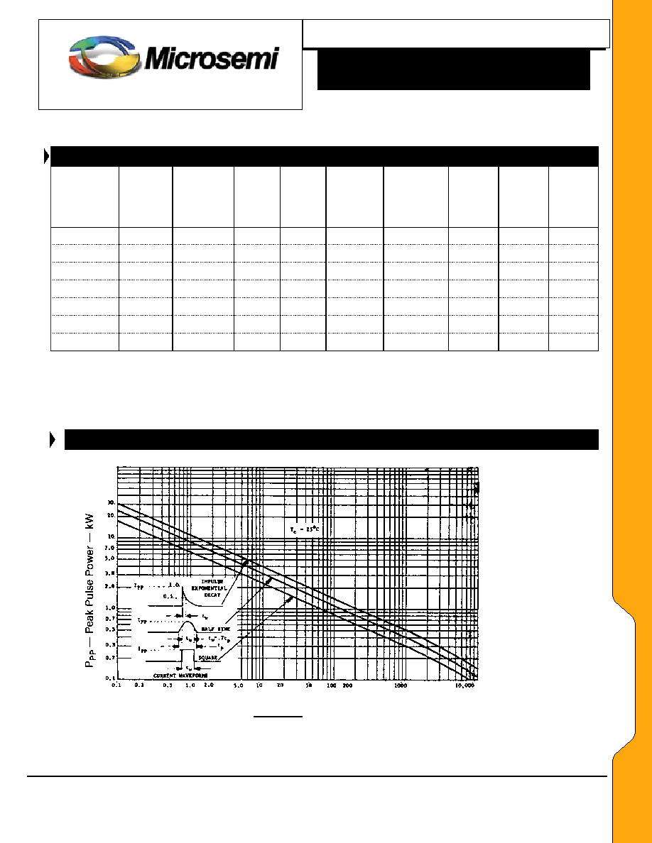
*See Figure 3
Clamping Factor: The ratio of the numerical value of V
C
to V
(BR)
is typically 1.4 @ full rated power, 1.20 @ 50% rated power. Also see MicroNote 108.
Note 1: A transient voltage suppressor is normally selected according to voltage (V
WM
), that should be equal to or greater than the dc or continuous
peak operating voltage level.
Note
2: When pulse testing, test in TVS avalanche direction. Do not pulse in "forward" direction. See section for "Schematic Applications" herein.
.
GRAPHS
t
w
� Pulse Width
�s
FIGURE 1
Microsemi
Scottsdale Division
8700 E. Thomas Rd. PO Box 1390, Scottsdale, AZ 85252 USA, (480) 941-6300, Fax: (480) 947-1503
Page 2
Copyright
2002
11-24-2003 REV A
Microsemi
Scottsdale Division
8700 E. Thomas Rd. PO Box 1390, Scottsdale, AZ 85252 USA, (480) 941-6300, Fax: (480) 947-1503
Page 3
Copyright
2002
11-24-2003 REV A
W
W
W
.
Mi
c
r
o
s
e
m
i
.
C
O
M
HSMBJSAC5.0 thru HSMBJSAC50
500 WATT LOW CAPACITANCE
TRANSIENT VOLTAGE SUPPRESSOR
S C O T T S D A L E D I V I S I O N
HSMBJSAC5.0 thru
H
S
MB
JS
A
C50
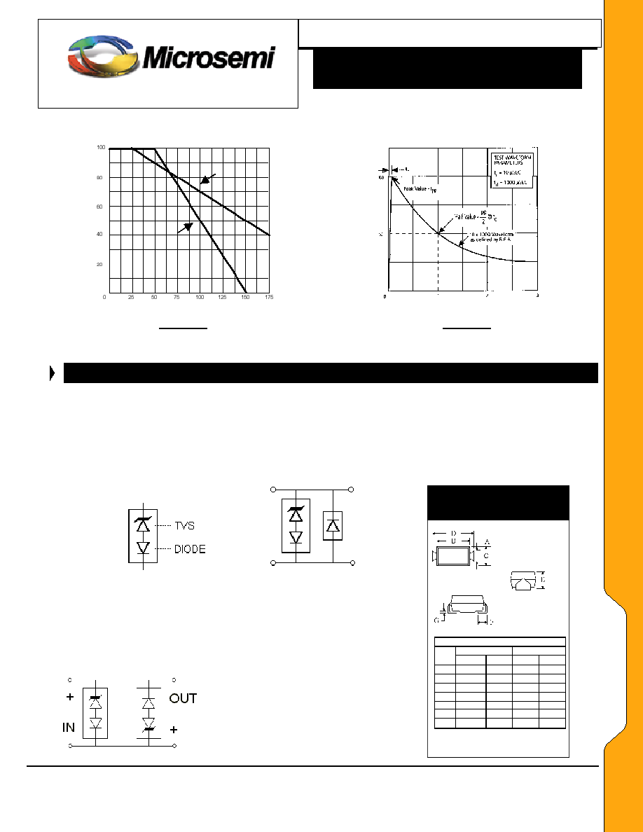
Peak Power
(Single Pulse)
I
PP
�
P
eak
Pulse
C
urre
nt
-
%I
PP
% of Rate
d Po
wer
Average
Power
T
L
� Lead Temperature �
o
C
t � Time � msec
FIGURE 2 FIGURE
3
Lead Length = 3/8
"
SCHEMATIC APPLICATIONS
The TVS low capacitance device configuration is shown in Figure 4. As a further option for unidirectional applications, an additional low
capacitance rectifier diode may be used in parallel in the same polarity direction as the TVS as shown in in Figure 5. In applications where
random high voltage transients occur, this will prevent reverse transients from damaging the internal low capacitance rectifier diode and also
provide a low voltage conducting direction. The added rectifier diode should be of similar low capacitance and also have a higher reverse voltage
rating than the TVS clamping voltage V
C
. Consult factory for recommended rectifier part number. If using two (2) low capacitance TVS devices
in anti-parallel for bidirectional applications, this added protective feature for both directions (including the reverse of each rectifier diode) is also
provided. The unidirectional and bidirectional configurations in Figure 5 and 6 will both result in twice the capacitance of Figure 4.
FIGURE 4
FIGURE 5
TVS with internal Low
Optional Unidirectional
Capacitance Diode
configuration (TVS and
separate
rectifier
diode)
PACKAGE
DIMENSIONS
DIMENSIONS
INCHES MILLIMETERS
DIM
MIN MAX
MIN MAX
A .073 .087 1.85 2.21
B .160 .180 4.06 4.57
C .130 .155 3.30 3.94
D .205 .220 5.21 5.59
E .075 .130 1.91 3.30
F .030 .060 .76 1.52
G .006 .016 .15 .41
NOTE: Dimension E exceeds the
JEDEC outline in height as shown
in
parallel)
FIGURE 6 Optional Bidirectional
configuration (two TVS devices in
anti-parallel)