 | –≠–ª–µ–∫—Ç—Ä–æ–Ω–Ω—ã–π –∫–æ–º–ø–æ–Ω–µ–Ω—Ç: LX1555 | –°–∫–∞—á–∞—Ç—å:  PDF PDF  ZIP ZIP |
Copyright © 1994
Rev. 1.0a 1/01
F O R F U R T H E R I N F O R M A T I O N C A L L ( 7 1 4 ) 8 9 8 - 8 1 2 1
11861 W
ESTERN
A
VENUE
, G
ARDEN
G
ROVE
, CA. 92841
1
U
LTRA
-L
OW
S
TART
-U
P
C
URRENT
, C
URRENT
-M
ODE
PWM
P
R O D U C T I O N
D
A T A
S
H E E T
T
H E
I
N F I N I T E
P
O W E R
O F
I
N N O V A T I O N
LX1552/3/4/5
LIN D
O C
#: 1552
D E S C R I P T I O N
K E Y F E A T U R E S
s
s
s
s
s ULTRA-LOW START-UP CURRENT
(150µA typ.)
s
s
s
s
s TRIMMED OSCILLATOR DISCHARGE
CURRENT
(±2% typ.)
s
s
s
s
s INITIAL OSCILLATOR FREQUENCY BETTER
THAN ±4%
s
s
s
s
s OUTPUT PULLDOWN DURING UVLO
s
s
s
s
s PRECISION 2.5V REFERENCE (±2% max.)
p CURRENT SENSE DELAY TO OUTPUT
(150ns typ.)
p AUTOMATIC FEED FORWARD
COMPENSATION
p PULSE-BY-PULSE CURRENT LIMITING
p ENHANCED LOAD RESPONSE
CHARACTERISTICS
p UNDER-VOLTAGE LOCKOUT WITH
HYSTERESIS
p DOUBLE PULSE SUPPRESSION
p HIGH CURRENT TOTEM POLE OUTPUT
(±1Amp peak)
p 500kHz OPERATION
The LX155X family of ultra-low start-up
current (250µA max.), current mode
control IC's offer new levels of energy
efficiency for offline converter applica-
tions. They are ideally optimized for
personal computer and CRT power
supplies although they can be used in
any number of off-line applications
where energy efficiency is critical.
Coupled with the fact that the LX155X
series requires a minimal set of external
components, the series offers an
excellent value for cost conscious
consumer applications.
Optimizing energy efficiency, the
LX155X series demonstrates a signifi-
cant power reduction as compared with
other similar off-line controllers. Table 1
compares the SG384X, UC384XA and
the LX155X start-up resistor power
dissipation. The LX155X offers an
overall 4X reduction in power dissipa-
tion. Additionally, the precise oscillator
discharge current gives the power
supply designer considerable flexibility
in optimizing system duty cycle
consistency.
The current mode architecture
demonstrates improved load regulation,
pulse by pulse current limiting and
inherent protection of the power supply
output switch. The LX155X includes a
bandgap reference trimmed to 1%, an
error amplifier, a current sense com-
parator internally clamped to 1V, a high
current totem pole output stage for fast
switching of power mosfet's, and an
externally programmable oscillator to
set operating frequency and maximum
duty cycle. The undervoltage lock-out
circuitry is designed to operate with as
little as 250µA of supply current
permitting very efficient bootstrap
designs.
P R O D U C T H I G H L I G H T
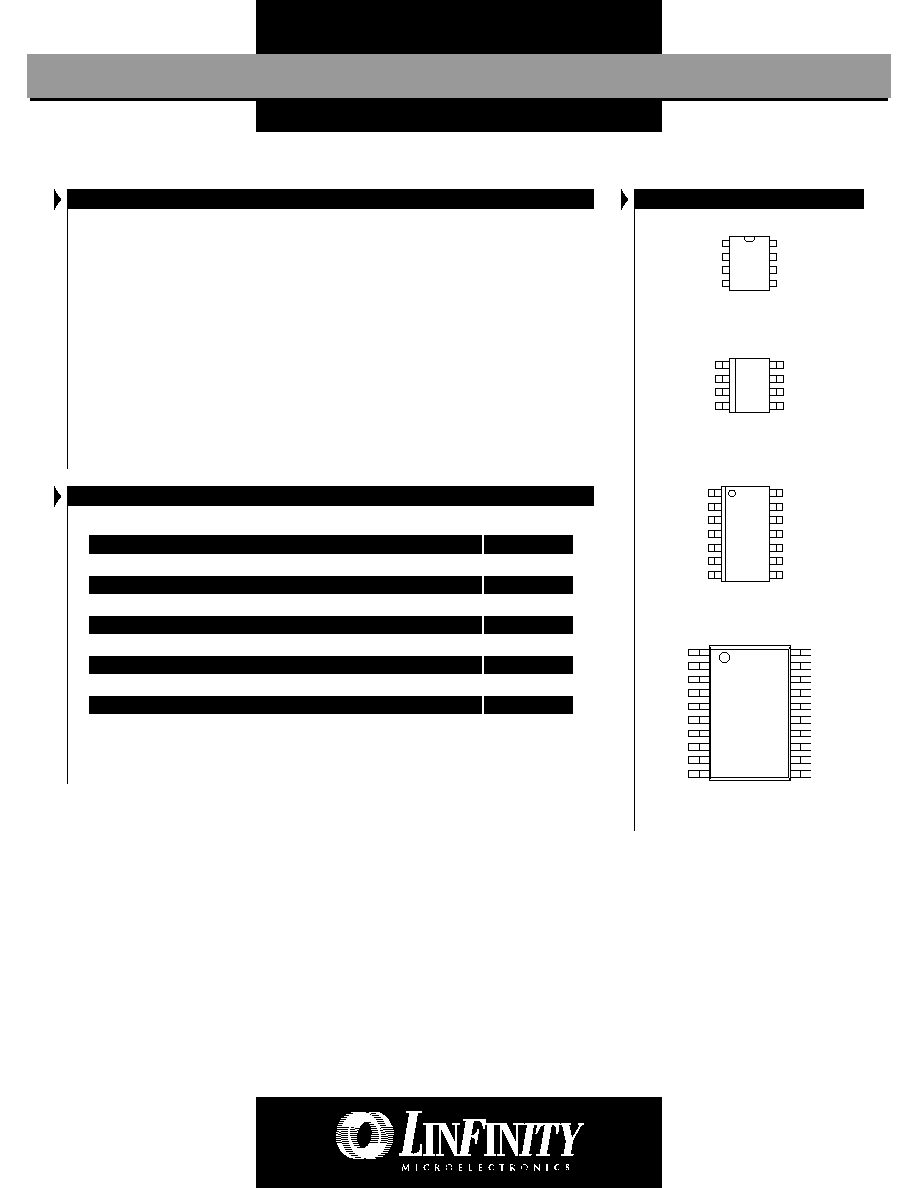
P A C K A G E O R D E R I N F O R M A T I O N
T
A
(∞C)
Plastic DIP
8-pin
0 to 70 LX155xCM LX155xCDM LX155xCD -- LX155xCPW
-40 to 85 LX155xIM LX155xIDM LX155xID -- --
-55 to 125 -- -- -- LX155xMY --
M
Plastic SOIC
8-pin
DM
Plastic SOIC
14-pin
D
Ceramic DIP
8-pin
Y
TSSOP
20-pin
PW
T
YPICAL
A
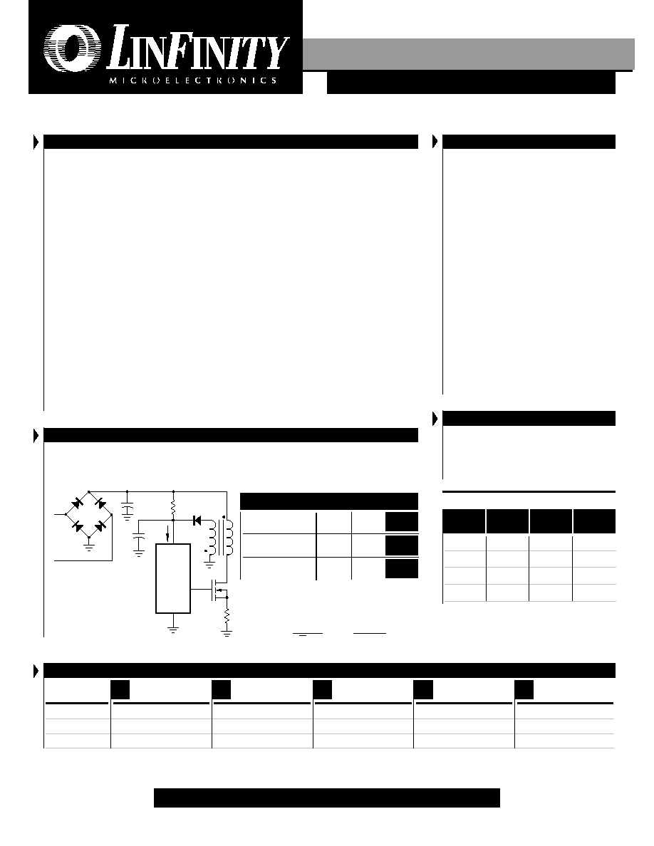
PPLICATION
OF
LX155X U
SING
I
TS
M
ICRO
P
OWER
S
TART
-U
P
F
EATURE
Max. Start-up Current
Specification (I
ST
)
Typical Start-Up
Resistor Value (R
ST
)
Max. Start-Up Resistor
Power Dissipation (P
R
)
Design Using SG384x UC384xA LX155x
1000µA 500µA
250µA
2.26W 1.13W
0.56W
62K
124K
248K
Note: Calculation is done for universal AC input speci-
fication of V
ACMIN
= 90V
RMS
to V
ACMAX
= 265V
RMS
using the
following equation: (Resistor curr ent is selected to be
2 * I
ST
at V
ACMIN
.)
R
ST
=
, P
R
=
V
AC MIN
2 * I
ST
2V
AC
2
MAX
R
ST
T
A B L E
1
A P P L I C A T I O N S
s
s
s
s
s ECONOMY OFF-LINE FLYBACK OR
FORWARD CONVERTERS
s DC-DC BUCK OR BOOST CONVERTERS
s LOW COST DC MOTOR CONTROL
A
V A I L A B L E
O
P T I O N S
P E R
P
A R T
#
Part # Start-Up Hysteresis Max. Duty
Voltage Cycle
LX1552 16V 6V <100%
LX1553 8.4V 0.8V <100%
LX1554 16V 6V <50%
LX1555 8.4V 0.8V <50%
I
ST
R
ST
V
CC
AC
INPUT
LX1552
or
LX1554
Note: All surface-mount packages are available in Tape & Reel. Append the letter "T" to part number. (i.e. LX1552CDMT)
U
LTRA
-L
OW
S
TART
-U
P
C
URRENT
, C
URRENT
-M
ODE
PWM
LX1552/3/4/5
P R O D U C T D A T A B O O K 1 9 9 6 / 1 9 9 7
Copyright © 1994
Rev. 1.0a 1/01
2
P
R O D U C T I O N
D
A T A
S
H E E T
ABSOLUTE MAXIMUM RATINGS
(Note 1)
Supply Voltage (Low Impedance Source) .................................................................. 30V
Supply Voltage (I
CC
< 30mA) ......................................................................... Self Limiting
Output Current ............................................................................................................. ±1A
Output Energy (Capacitive Load) ................................................................................ 5µJ
Analog Inputs (Pins 2, 3) ........................................................................... -0.3V to +6.3V
Error Amp Output Sink Current ............................................................................... 10mA
Power Dissipation at T
A
= 25∞C (DIL-8) ...................................................................... 1W
Operating Junction Temperature
Ceramic (Y Package) ............................................................................................ 150∞C
Plastic (M, DM, D, PW Packages) ........................................................................ 150∞C
Storage Temperature Range .................................................................... -65∞C to +150∞C
Lead Temperature (Soldering, 10 Seconds) ............................................................ 300∞C
PACKAGE PIN OUTS
V
REF
V
CC
OUTPUT
GND
COMP
V
FB
I
SENSE
R
T
/C
T
1
8
2
7
3
6
4
5
M & Y PACKAGE
(Top View)
DM PACKAGE
(Top View)
V
REF
V
CC
OUTPUT
GND
COMP
V
FB
I
SENSE
R
T
/C
T
1
8
2
7
3
6
4
5
V
REF
N.C.
V
CC
V
C
OUTPUT
GND
PWR GND
COMP
N.C.
V
FB
N.C.
I
SENSE
N.C.
R
T
/C
T
1
14
2
13
3
12
4
11
5
10
6
9
7
8
D PACKAGE
(Top View)
PW PACKAGE
(Top View)
1
20
2
19
3
18
4
17
5
16
6
15
7
14
8
13
9
12
10 11
N.C.
N.C.
COMP
V
FB
N.C.
I
SENSE
N.C.
R
T
/C
T
N.C.
N.C.
N.C.
N.C.
V
REF
N.C.
V
CC
V
C
OUTPUT
GND
PWR GND
N.C.
M PACKAGE:
THERMAL RESISTANCE-JUNCTION TO AMBIENT,
JA
95∞C/W
DM PACKAGE:
THERMAL RESISTANCE-JUNCTION TO AMBIENT,
JA
165∞C/W
D PACKAGE:
THERMAL RESISTANCE-JUNCTION TO AMBIENT,
JA
120∞C/W
Y PACKAGE:
THERMAL RESISTANCE-JUNCTION TO AMBIENT,
JA
130∞C/W
PW PACKAGE:
THERMAL RESISTANCE-JUNCTION TO AMBIENT,
JA
144∞C/W
Junction Temperature Calculation: T
J
= T
A
+ (P
D
x
JA
).
The
JA
numbers are guidelines for the thermal performance of the device/pc-board system.
All of the above assume no ambient airflow
THERMAL DATA
Note 1. Exceeding these ratings could cause damage to the device. All voltages are with respect
to Ground. Currents are positive into, negative out of the specified terminal. Pin
numbers refer to DIL packages only.
U
LTRA
-L
OW
S
TART
-U
P
C
URRENT
, C
URRENT
-M
ODE
PWM
LX1552/3/4/5
P R O D U C T D A T A B O O K 1 9 9 6 / 1 9 9 7
3
Copyright © 1994
Rev. 1.0a 1/01
P
R O D U C T I O N
D
A T A
S
H E E T
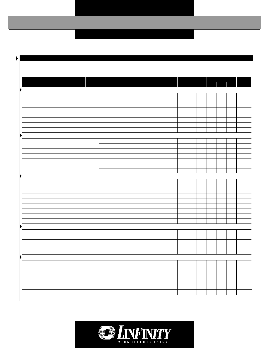
E L E C T R I C A L C H A R A C T E R I S T I C S
(Unless otherwise specified, these specifications apply over the operating ambient temperatures for LX155xC with 0∞C
T
A
70∞C, LX155xI with -40∞C
T
A
85∞C, LX155xM
with -55∞C
T
A
125∞C; V
CC
=15V (Note 5); R
T
=10K; C
T
=3.3nF. Low duty cycle pulse testing techniques are used which maintains junction and case temperatures equal to the
ambient temperature.)
Reference Section
Parameter Symbol Test Conditions
Output Voltage V
REF
T
A
= 25∞C, I
L
= 1mA
Line Regulation 12
V
IN
25V
Load Regulation 1
I
O
20mA
Temperature Stability (Note 2 & 7)
Total Output Variation Over Line, Load, and Temperature
Output Noise Voltage (Note 2) V
N
10Hz
f
10kHz, T
A
= 25∞C
Long Term Stability (Note 2) T
A
= 125∞C, t = 1000hrs
Output Short Circuit I
SC
LX155xC
Units
Min. Typ. Max. Min. Typ. Max.
LX155xI/155xM
4.95
5.00
5.05
4.95
5.00
5.05 V
6
20
6
20
mV
6
25
6
25
mV
0.2 0.4 0.2 0.4 mV/∞C
4.9 5.1 4.9 5.1 V
50 50 µV
5
25
5
25
mV
-30 -100 -180 -30 -100 -180 mA
Oscillator Section
Initial Accuracy (Note 6) T
A
= 25∞C
T
A
= 25∞C, R
T
= 698
, C
T
= 22nF, LX1552/3 only
Voltage Stability 12
V
CC
25V
Temperature Stability (Note 2) T
MIN
T
A
T
MAX
Amplitude (Note 2) V
PIN 4
peak to peak
Discharge Current I
D
T
A
= 25∞C, V
PIN 4
= 2V
V
PIN 4
= 2V, T
MIN
T
A
T
MAX
48.5
50.5
52.5
48.5
50.5
52.5 kHz
56 58 60 56 58 60 kHz
0.2 1 0.2 1 %
5
5
%
1.7 1.7 V
8.0 8.3 8.6 8.0 8.3 8.6 mA
7.6 8.8 7.8 8.8 mA
Output Voltage Low Level V
OL
I
SINK
= 20mA
I
SINK
= 200mA
Output Voltage High Level V
OH
I
SOURCE
= 20mA
I
SOURCE
= 200mA
Rise Time (Note 2) T
R
T
A
= 25∞C, C
L
= 1nF
Fall Time (Note 2) T
F
T
A
= 25∞C, C
L
= 1nF
UVLO Saturation V
SAT
V
CC
= 5V, I
SINK
= 10mA
Error Amp Section
Current Sense Section
Gain (Note 3 & 4) A
VOL
Maximum Input Signal (Note 3) V
PIN 1
= 5V
Power Supply Rejection Ratio (Note 3) PSRR 12
V
CC
25V
Input Bias Current I
B
Delay to Output (Note 2) T
PD
V
PIN 3
= 0 to 2V
Output Section
2.45
2.50
2.55
2.45
2.50
2.55 V
-0.1 -1 -0.1 -0.5 µA
65 90 65 90 dB
0.6 0.6 MHz
60 70 60 70 dB
2
4
2
4
mA
-0.5 -0.8 -0.5 -0.8 mA
5 6.5 5 6.5 V
0.7 1.1 0.7 1.1 V
2.85 3 3.15
2.85 3 3.15 V/V
0.9 1 1.1 0.9 1 1.1 V
70 70 dB
-2 -10 -2 -5 µA
150 300 150 300 ns
0.1 0.4 0.1 0.4 V
1.5 2.2 1.5 2.2 V
13 13.5 13 13.5 V
12 13.5 12 13.5 V
50 100 50 100 ns
50 100 50 100 ns
0.7 1.2 0.7 1.2 V
( E l e c t r i c a l C h a r a c t e r i s t i c s c o n t i n u e n e x t p a g e . )
Input Voltage V
PIN 1
= 2.5V
Input Bias Current I
B
Open Loop Gain A
VOL
2
V
O
4V
Unity Gain Bandwidth (Note 2) UGBW T
A
= 25∞C
Power Supply Rejection Ratio (Note 3) PSRR 12
V
CC
25V
Output Sink Current I
OL
V
PIN 2
= 2.7V, V
PIN 1
= 1.1V
Output Source Current I
OH
V
PIN 2
= 2.3V, V
PIN 1
= 5V
Output Voltage High Level V
OH
V
PIN 2
= 2.3V, R
L
= 15K to ground
Output Voltage Low Level V
OL
V
PIN 2
= 2.7V, R
L
= 15K to V
REF

U
LTRA
-L
OW
S
TART
-U
P
C
URRENT
, C
URRENT
-M
ODE
PWM
LX1552/3/4/5
P R O D U C T D A T A B O O K 1 9 9 6 / 1 9 9 7
Copyright © 1994
Rev. 1.0a 1/01
4
P
R O D U C T I O N
D
A T A
S
H E E T
E L E C T R I C A L C H A R A C T E R I S T I C S
(Con't.)
Under-Voltage Lockout Section
Parameter Symbol Test Conditions
Start Threshold V
ST
1552/1554
1553/1555
Min. Operation Voltage After Turn-On 1552/1554
1553/1555
LX155xC
Units
Min. Typ. Max. Min. Typ. Max.
LX155xI/155xM
15 16 17 15 16 17 V
7.8 8.4 9.0 7.8 8.4 9.0 V
9 10 11 9 10 11 V
7.0 7.6 8.2 7.0 7.6 8.2 V
PWM Section
Maximum Duty Cycle 1552/1553
1552/1553, R
T
= 698
, C
T
= 22nF
1554/1555
Minimum Duty Cycle
94 96 94 96 %
50 50 %
47 48 47 48 %
0
0
%
Power Consumption Section
Start-Up Current I
ST
Operating Supply Current I
CC
V
CC
Zener Voltage V
Z
I
CC
= 25mA
150 250 150 250 µA
11 17 11 17 mA
30 35 30 35 V
Notes: 2. These parameters, although guaranteed, are not 100% tested in
production.
3. Parameter measured at trip point of latch with V
FB
= 0.
4. Gain defined as: A = ; 0
V
ISENSE
0.8V.
5. Adjust V
CC
above the start threshold before setting at 15V.
6. Output frequency equals oscillator frequency for the LX1552 and
LX1553. Output frequency is one half oscillator frequency for the
LX1554 and LX1555.
7. Temperature stability, sometimes referred to as average temperature
coefficient, is described by the equation:
Temp Stability =
V
REF
(max.) & V
REF
(min.) are the maximum & minimum reference
voltage measured over the appropriate temperature range. Note that the
extremes in voltage do not necessarily occur at the extremes in
temperature.
V
REF
(max.) - V
REF
(min.)
T
A
(max.) - T
A
(min.)
V
COMP
V
ISENSE
B L O C K D I A G R A M
* - V
CC
and V
C
are internally connected for 8 pin packages.
** - POWER GROUND and GROUND are internally connected for 8 pin packages.
*** - Toggle flip flop used only in 1554 and 1555.
OSCILLATOR
S
R
***
V
REF
GOOD LOGIC
INTERNAL
BIAS
S / R
5V
REF
PWM
LATCH
CURRENT SENSE
COMPARATOR
1V
R
2R
ERROR AMP
16V (1552/1554)
8.4V (1553/1555)
16V (1552/1554)
8.4V (1553/1555)
UVLO
34V
GROUND**
V
CC
*
R
T
/C
T
V
FB
T
COMP
I
SENSE
POWER GROUND**
OUTPUT
V
C
*
V
REF

U
LTRA
-L
OW
S
TART
-U
P
C
URRENT
, C
URRENT
-M
ODE
PWM
LX1552/3/4/5
P R O D U C T D A T A B O O K 1 9 9 6 / 1 9 9 7
5
Copyright © 1994
Rev. 1.0a 1/01
P
R O D U C T I O N
D
A T A
S
H E E T
GRAPH / CURVE INDEX
Characteristic Curves
FIGURE #
1. OSCILLATOR FREQUENCY vs. TIMING RESISTOR
2. MAXIMUM DUTY CYCLE vs. TIMING RESISTOR
3. OSCILLATOR DISCHARGE CURRENT vs. TEMPERATURE
4. OSCILLATOR FREQUENCY vs. TEMPERATURE
5. OUTPUT INITIAL ACCURACY vs. TEMPERATURE
6. OUTPUT DUTY CYCLE vs. TEMPERATURE
7. REFERENCE VOLTAGE vs. TEMPERATURE
8. REFERENCE SHORT CIRCUIT CURRENT vs. TEMPERATURE
9. E.A. INPUT VOLTAGE vs. TEMPERATURE
10. START-UP CURRENT vs. TEMPERATURE
11. START-UP CURRENT vs. SUPPLY VOLTAGE
12. START-UP CURRENT vs. SUPPLY VOLTAGE
13. DYNAMIC SUPPLY CURRENT vs. OSCILLATOR FREQUENCY
14. CURRENT SENSE DELAY TO OUTPUT vs. TEMPERATURE
15. CURRENT SENSE THRESHOLD vs. ERROR AMPLIFIER OUTPUT
16. START-UP THRESHOLD vs. TEMPERATURE
17. START-UP THRESHOLD vs. TEMPERATURE
18. MINIMUM OPERATING VOLTAGE vs. TEMPERATURE
19. MINIMUM OPERATING VOLTAGE vs. TEMPERATURE
20. LOW LEVEL OUTPUT SATURATION VOLTAGE DURING UNDER-
VOLTAGE LOCKOUT
21. OUTPUT SATURATION VOLTAGE vs. OUTPUT CURRENT and
TEMPERATURE
22. OUTPUT SATURATION VOLTAGE vs. OUTPUT CURRENT and
TEMPERATURE
FIGURE INDEX
Theory of Operation Section
FIGURE #
23. TYPICAL APPLICATION OF START-UP CIRCUITRY
24. REFERENCE VOLTAGE vs. TEMPERATURE
25. SIMPLIFIED SCHEMATIC OF OSCILLATOR SECTION
26. DUTY CYCLE VARIATION vs. DISCHARGE CURRENT
27. OSCILLATOR FREQUENCY vs. TIMING RESISTOR
28. MAXIMUM DUTY CYCLE vs. TIMING RESISTOR
29. CURRENT SENSE THRESHOLD vs. ERROR AMPLIFIER OUTPUT
Typical Applications Section
FIGURE #
30. CURRENT SENSE SPIKE SUPPRESSION
31. MOSFET PARASITIC OSCILLATIONS
32. ADJUSTABLE BUFFERED REDUCTION OF CLAMP LEVEL
WITH SOFT-START
33. EXTERNAL DUTY CYCLE CLAMP AND MULTI-UNIT SYCHRONIZATION
34. SLOPE COMPENSATION
35. OPEN LOOP LABORATORY FIXTURE
36. OFF-LINE FLYBACK REGULATOR