L
OW
V
OLTAGE
A
DJUSTABLE
P
RECISION
S
HUNT
R
EGULATORS
P
R O D U C T I O N
D
A T A
S
H E E T
T
H E
I
N F I N I T E
P
O W E R
O F
I
N N O V A T I O N
LX432
D E S C R I P T I O N
K E Y F E A T U R E S
s Low Voltage Operation: 1.24V Reference
s Initial Voltage Reference Accuracy 1%
s Adjustable Output Voltage From V
REF
To 20V
s Typical Output Dynamic Impedance Less
Than 250m
s Sink Current Capability 80�A To 20mA
s Direct Alternative To TLV431
Low voltage operation enables the
LX432 to be used in the feedback loop
of isolated low voltage power sup-
plies. The minimum output voltage is
determined by the LX432 output voltage
plus the forward voltage drop of the
opto-coupler LED (typically 1.24 + 1.4 =
2.64V minimum). See Figure 10.
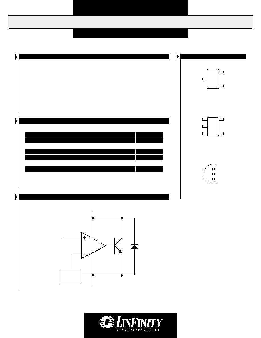
The LX432 is offered in 3 and 5-pin
SOT-23 or TO-92 packages, and is a drop-
in replacement for the TLV431 and
SC431L devices.
The LX432 series are low-voltage pre-
cision adjustable shunt regulators
with a reference voltage of 1.24V. The
output voltage may be set to any value
between 1.24V and 20V by two external
resistors.
These devices offer low output im-
pedance for improved load regula-
tion -- typical output impedance is
250m
. The LX432 series operates with
an operating current as low as 80�A,
making these devices suitable for por-
table and micropower applications.
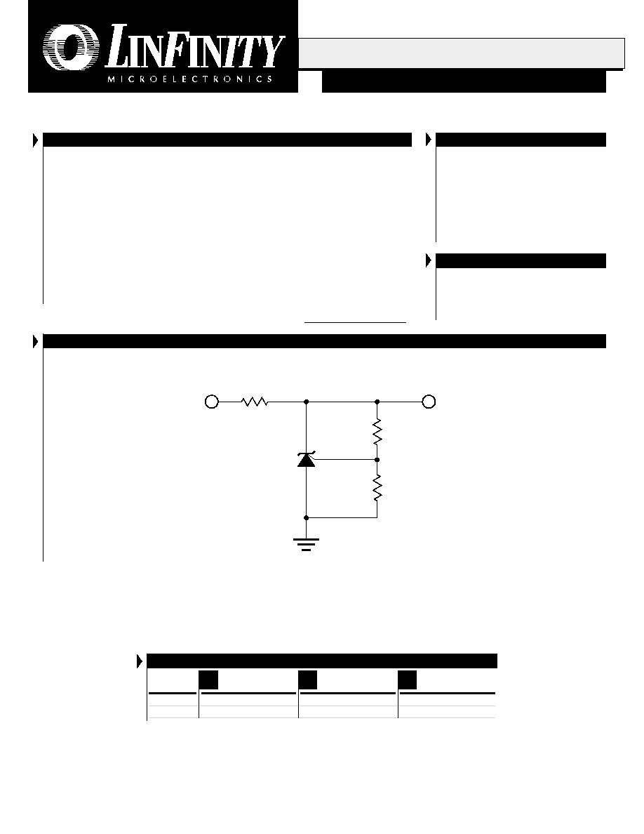
P R O D U C T H I G H L I G H T
T
Y P I C A L
P
R O G R A M M A B L E
V
O L T A G E
R
E F E R E N C E
C
I R C U I T
P A C K A G E O R D E R I N F O R M A T I O N
T
A
(�C)
Plastic SOT-23
3-pin
SC
Plastic SOT-23
5-pin
SE
0 to 70
LX432CSC
LX432CSE
LX432CLP
-40 to 85
LX432ISC
LX432ISE
LX432ILP
Note: All surface-mount packages are available in Tape & Reel.
Append the letter "T" to part number. (i.e. LX432CSET)
TO-92 (LP) package also available in ammo-pack.
Copyright � 1999
Rev. 1.0 9/99
1
11861 W
ESTERN
A
VENUE
, G
ARDEN
G
ROVE
, CA. 92841, 714-898-8121, F
AX
: 714-893-2570
L
I N
F
I N I T Y
M
I C R O E L E C T R O N I C S
I
N C
.
A P P L I C A T I O N S
s Low Voltage Adjustable Power Supplies
s Instrumentation
s Computers
s Portable Equipment
LX432
R1
R2
GND
V
KA
V
IN
Cathode
Anode
Reference
IMPORTANT: For the most current data, consult LinFinity's web site: http://www.linfinity.com.
Plastic TO-92
3-pin
LP
L
OW
V
OLTAGE
A
DJUSTABLE
P
RECISION
S
HUNT
R
EGULATORS
LX432
P R O D U C T D A T A B O O K 1 9 9 6 / 1 9 9 7
Copyright � 1999
Rev. 1.0 9/99
2
P
R O D U C T I O N
D
A T A
S
H E E T
ABSOLUTE MAXIMUM RATINGS
(Note 1)
Cathode to Anode Voltage (V
KA
) ................................................................. -0.3V to +20V
Reference Input Current (I
REF
) .................................................................... -50�A to 10�A
Continuous Cathode Current (I
K
) ............................................................. -25mA to 25mA
Operating Junction Temperature
Plastic (SC, SE & LP Packages) ............................................................................. 150�C
Storage Temperature Range ...................................................................... -65�C to 150�C
Lead Temperature ..................................................................................................... 300�C
PACKAGE PIN OUTS
LP PACKAGE
(Top View)
3. CATHODE
2. ANODE
1. REF
SC PACKAGE -- 3-Pin
(Top View)
Note 1. Exceeding these ratings could cause damage to the device. All voltages are with respect
to Ground. Currents are positive into, negative out of the specified terminal. Pin
numbers refer to DIL packages only.
SC PACKAGE:
Thermal Resistance - Junction to Ambient,
JA
(PC-Mounted)
220�C/W
(Non-PC Mounted)
410�C/W
SE PACKAGE:
Thermal Resistance - Junction to Ambient,
JA
(PC-Mounted)
220�C/W
(Non-PC Mounted)
410�C/W
LP PACKAGE:
Thermal Resistance-Junction to Ambient,
JA
156�C/W
Junction Temperature Calculation: T
J
= T
A
+ (P
D
x
JA
).
The
JA
numbers are guidelines for the thermal performance of the device/pc-board system.
All of the above assume no ambient airflow
THERMAL DATA
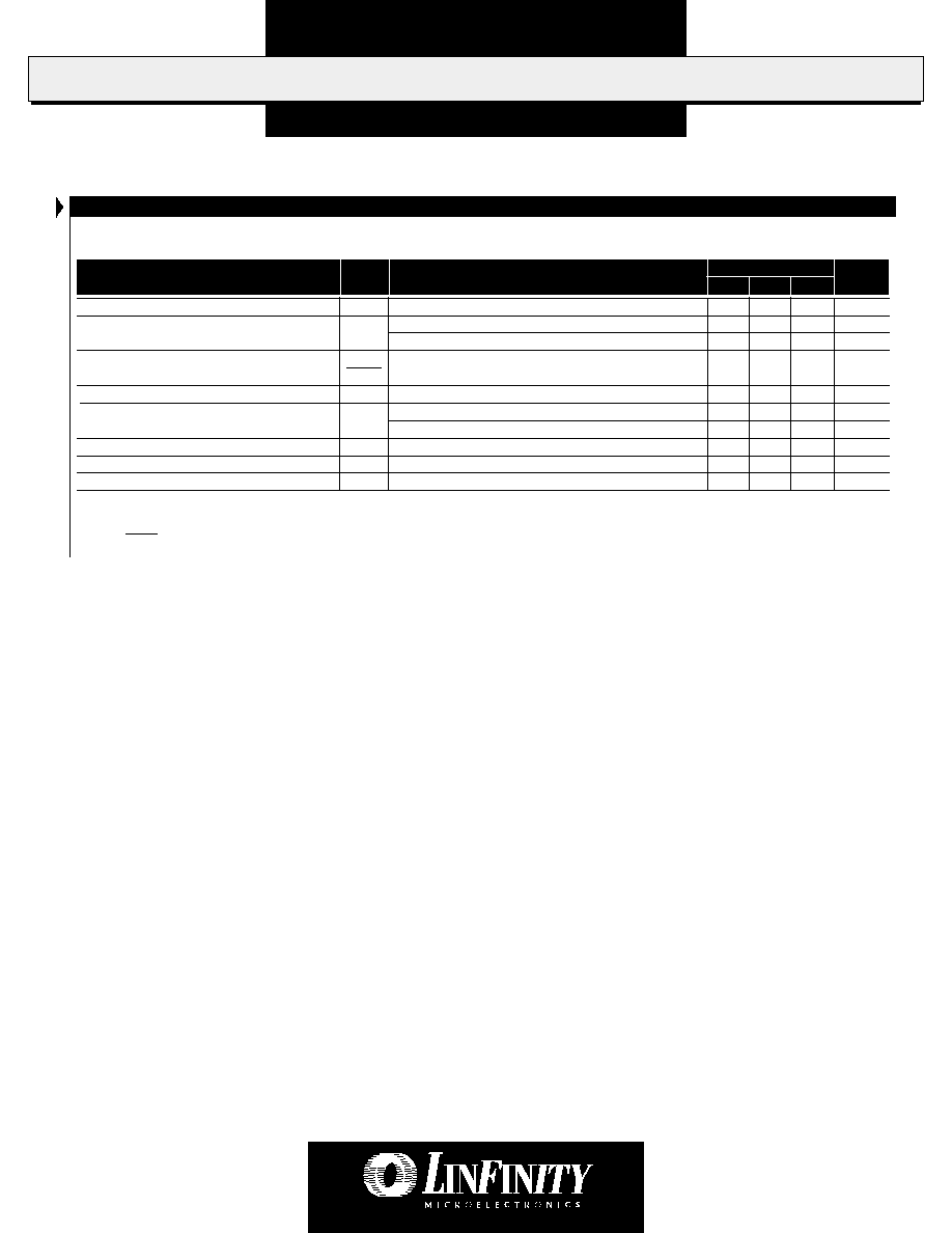
BLOCK DIAGRAM
Cathode (K)
Anode (A)
V
REF
Ref (R)
CATHODE
REF
ANODE
SE PACKAGE -- 5-Pin
(Top View)
ANODE
REF
N.C.
N.C.
CATHODE
1
5
2
3
4
2
3
1
L
OW
V
OLTAGE
A
DJUSTABLE
P
RECISION
S
HUNT
R
EGULATORS
LX432
P R O D U C T D A T A B O O K 1 9 9 6 / 1 9 9 7
3
Copyright � 1999
Rev. 1.0 9/99
P
R O D U C T I O N
D
A T A
S
H E E T
E L E C T R I C A L C H A R A C T E R I S T I C S
(Unless otherwise specified, these specifications apply over the operating ambient temperatures for LX432C with 0�C
T
A
70�C, and the LX432I
with -40�C
T
A
85�C.)
Parameter
Symbol
Test Conditions
LX432
Units
Min.
Typ.
Max.
1.228
1.24
1.252
V
3
12
mV
4
20
mV
-1
-2.7
mV/V
0.1
0.5
�A
0.05
0.3
�A
0.1
0.4
�A
55
80
�A
0.2
0.4
0.004
�A
Reference Voltage
V
REF
I
K
= 10mA, V
KA
= V
REF
, T
A
= 25�C
Reference Voltage Drift
(Note 2)
V
REF
I
K
= 10mA, V
KA
= V
REF
, 0�C
T
A
70�C
I
K
= 10mA, V
KA
= V
REF
, -40�C
T
A
85�C
Ratio Of V
REF
Change In Cathode
V
REF
I
K
= 10mA, V
KA
= V
REF
to 16V, T
A
= 25�C
Voltage Change
(Note 3)
V
KA
Reference Terminal Current
I
REF
I
K
= 10mA, V
KA
= V
REF
, T
A
= 25�C, R1=10k
, R2 = Open
Reference Current Drift
(Note 2)
I
REF
I
K
= 10mA, V
KA
= V
REF
, 0�C
T
A
70�C
I
K
= 10mA, V
KA
= V
REF
, -40�C
T
A
85�C
Minimum Cathode Current For Regulation
I
K (MIN)
V
KA
= V
REF
, T
A
= 25�C
Dynamic Impedance
Z
KA
I
K
= 0.1mA to 15mA, V
KA
= V
REF
, T
A
= 25�C
Off-state Cathode Current
I
OFF
V
KA
= 16V, T
A
= 25�C
Note 2. These parameters are guaranteed by design.
Note 3.
Ratio of change in reference input voltage
to the change in cathode voltage.
V
REF
V
KA
L
OW
V
OLTAGE
A
DJUSTABLE
P
RECISION
S
HUNT
R
EGULATORS
LX432
P R O D U C T D A T A B O O K 1 9 9 6 / 1 9 9 7
Copyright � 1999
Rev. 1.0 9/99
4
P
R O D U C T I O N
D
A T A
S
H E E T
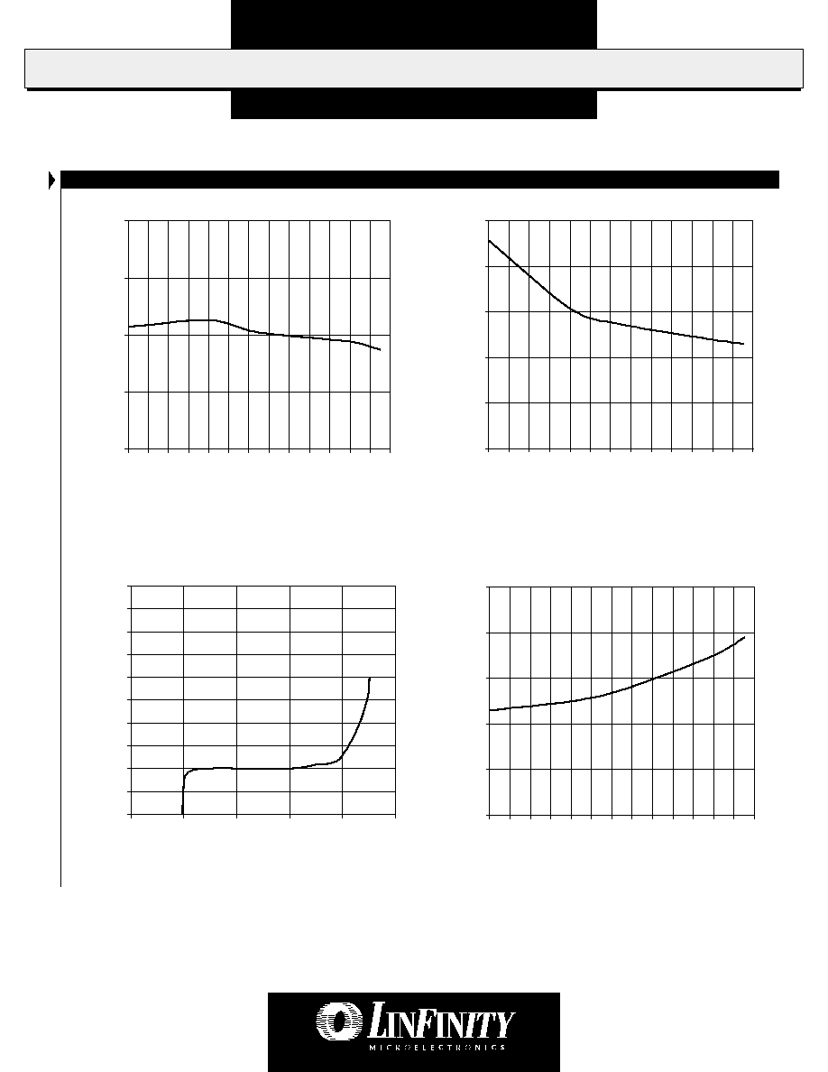
GRAPH / CURVE INDEX
Characteristic Curves
FIGURE #
1.
Reference Voltage vs. Junction Temperature
2.
Reference Current vs. Junction Temperature
3.
Cathode Current vs. Cathode Voltage
4.
V
REF
/
V
KA
vs. Junction Temperature
5.
Dynamic Impedance vs. Junction Temperature
6.
Minimum Cathode Current For Regulation vs. Junction
Temperature
7.
Off-State Current vs. Junction Temperature
8.
Equivalent Input Noise Voltage vs. Frequency
FIGURE INDEX
Parameter Measurement Information
FIGURE #
9.
Test Circuit For V
KA
= V
REF
10. Test Circuit For V
KA
> V
REF
11. Test Circuit For I
OFF
Typical Applications
FIGURE #
12. Flyback With Isolation Using LX431 Or LX431A As Voltage
Reference And Error Amplifier
13. LX432 In 3.3V To 2.7V Low Dropout Regulator Application
L
OW
V
OLTAGE
A
DJUSTABLE
P
RECISION
S
HUNT
R
EGULATORS
LX432
P R O D U C T D A T A B O O K 1 9 9 6 / 1 9 9 7
5
Copyright � 1999
Rev. 1.0 9/99
P
R O D U C T I O N
D
A T A
S
H E E T
C H A R A C T E R I S T I C C U R V E S
FIGURE 1 -- Reference Voltage vs. Junction Temperature
FIGURE 2 -- Reference Current vs. Junction Temperature
1.23
1.235
1.24
1.245
1.25
-40 -30 -20 -10
0
10 20 30 40 50 60
70 80 90
T
J
: Junction Temperature ( C)
V
REF
: Reference Voltage (V
)
0
0.04
0.08
0.12
0.16
0.2
-40 -30 -20 -10
0
10 20 30 40 50 60 70 80 90
T
J
: Junction Temperature ( C)
I
REF
: Reference Current (
A
)
FIGURE 3 -- Cathode Current vs. Cathode Voltage
FIGURE 4 --
V
REF
/
V
KA
vs. Junction Temperature
-200
-100
0
100
200
300
400
500
600
700
800
-1
-0.5
0
0.5
1
1.5
T
J
: Junction Temperature (V)
I
K
: Cathode Current (
A
)
-1.200
-1.000
-0.800
-0.600
-0.400
-0.200
-40 -30 -20 -10
0
10 20 30
40 50 60 70 80 90
T
J
: Junction Temperature ( C)
V
REF
/
V
KA
(mV/V)