 | –≠–ª–µ–∫—Ç—Ä–æ–Ω–Ω—ã–π –∫–æ–º–ø–æ–Ω–µ–Ω—Ç: LX5241 | –°–∫–∞—á–∞—Ç—å:  PDF PDF  ZIP ZIP |

� �
T
H E
I
N F I N I T E
P
O W E R O F
I
N N O V A T I O N
L
I N
F
I N I T Y
M
I C R O E L E C T R O N I C S
I
N C
.
11861 W
ESTERN
A
VENUE
, G
ARDEN
G
ROVE
, CA. 92841, 714-898-8121, F
AX
: 714-893-2570
1
Copyright
©
2000
Rev. 1.4,2000-11-28
TM
LX5241/5242/5243
�
The LX5241/42/43 is a multimode SCSI
terminator that is compatible with to the SCSI
SPI02 (Ultra2 SCSI), SCSI SPI-3 (Ultra3 SCSI or
Ultra160 SCSI), and pending SCSI SPI-4
(Ultra320) specifications developed by the T10
standards committee for low voltage differential
(LVD) termination, while providing backwards
compatibility to the SCSI, SCSI-2, and SPI single-
ended specifications. Multimode compatibility
permits the use of legacy devices on the bus
without hardware alterations. Automatic mode
selection is achieved through voltage detection on
the Diffsense line.
The LX5241/42/43 utilizes Linfinity's
UltraMAX technology which delivers the ultimate
in SCSI bus performance while saving component
cost and board area. Elimination of the external
capacitors also mitigates the need for a lengthy
capacitor selection process. The individual high
bandwidth drivers also maximize channel
separation and reduce channel to channel noise and
cross talk. The high bandwidth architecture insures
ULTRA2 performance while providing a clear
migration path to ULTRA3 and beyond.
When the LX5241/42/43 is enabled, the
differential sense (DIFFSENSE) pin supplies a
voltage between 1.2V and 1.4V. In application
this pin is tied to the DIFFSENSE input of the
corresponding LVD transceivers. This action
enables
the
LVD
transceiver
function.
DIFFSENSE is capable of supplying a maximum
of 15mA. Tying the DIFFSENSE pin high places
the LX5241/42/43 in a HI Z state indicating the
presence of an HVD device. Tying the pin low
places the part in a single-ended mode while also
signaling the multimode transceiver to operate in a
single-ended mode.
Recognizing the needs of portable and
configurable peripherals, the LX5241/42/43 have
a TTL compatible sleep/disable mode. During
this sleep/disable mode, power dissipation is
reduced to a meager 15uA while also placing all
outputs in a HI Z state. Also during sleep/disable
mode, the DIFFSENSE function is disabled and is
placed in a HI Z state.
Another key feature of the LX5241/42/43 is the
master / slave function. Driving this pin high or
floating the pin enables the 1.3V DIFFSENSE
reference. Driving the pin low disables the on
board DIFFSENSE reference and enables use of
an external master reference device.
IMPORTANT:
For the most current data, consult
MICROSEMI
's website: http://www.microsemi.com
�
�
Auto-Selectable LVD or Single-
Ended Termination
3.0pF Maximum Disabled Output
Capacitance
Fast Response, No External
Capacitors Required
Compatible with Active Negation
Drivers
15µA Supply Current in
Disconnect Mode
Logic Command Disconnects All
Termination Lines
Diffsense Line Driver
Ground Driver Integrated for
Single-Ended Operation
Current Limit and Thermal
Protection
Hot-Swap Compatible (Single-
Ended)
Ultra160 compliant
See LX5245/5246 for LVD
Termination Only
Pin Compatible With DS2119
and UCC5630
B
US
V
OLTAGE
6 V
OD
V
(+)
V
(-)
V
CM
0V
-100mV
100mV
V
OD
= V
(-)
- V
(+)
, Logic = 0
NEGATED
L X 5 2 4 1
L X 5 2 4 1
+
-
+
-
�
T
A
(
∞
C)
DB
Plastic TSSOP
36-Pin
PW
Plastic TSSOP
24-Pin
PW
Plastic TSSOP
28-Pin
LX5241CDBK LX5241CPWK LX5243CPW
0 to 70
LX5242CDBK LX5242CPWK
-
Note: Available in Tape & Reel.
Append the letter "T" to the part number. (i.e. LX5241CDBT)

M
U L T I M O D E
S C S I T
E R M I N A T O R
LX5241/5242/5243
P R O D U C T D A T A B O O K 1 9 9 6 / 1 9 9 7
Copyright © 2000
Rev. 1.4 11/00
2
P
R O D U C T I O N
D
A T A
S
H E E T
UltraMAX
TermPwr Voltage ................................................................................................. +7V
Operating Junction Temperature
Plastic (DB, PW Packages) .......................................................................... 150∞C
Storage Temperature Range .............................................................. -65∞C to 150∞C
Lead Temperature (Soldering, 10 seconds) .................................................... 300∞C
Note 1. Exceeding these ratings could cause damage to the device. All voltages are with
respect to Ground. Currents are positive into, negative out of the specified
terminal.
DB PACKAGE:
THERMAL RESISTANCE-JUNCTION TO AMBIENT,
JA
50∞C/W
PW PACKAGE:
THERMAL RESISTANCE-JUNCTION TO AMBIENT,
JA
100∞C/W
Junction Temperature Calculation: T
J
= T
A
+ (P
D
x
JA
).
The
JA
numbers are guidelines for the thermal performance of the device/pc-board
system. All of the above assume no ambient airflow.
THERMAL DATA
ABSOLUTE MAXIMUM RATINGS
(Note 1)
PACKAGE PIN OUTS
DB PACKAGE
(Top View)
LX5241/5242
("N.C." = No Internal Connection)
N.C.
N.C.
N.C.
1+
1-
2+
2-
HEATSINK
HEATSINK
HEATSINK
3+
3-
4+
4-
5+
5-
DISCONNECT
GND
V
TERM
HVD
LVD
SE
9-
9+
8-
8+
HEATSINK
HEATSINK
HEATSINK
7-
7+
6-
6+
DIFF B
DIFFSENSE
MASTER/SLAVE
1
36
2
35
3
34
4
33
5
32
631
7
30
8
29
9
28
10627
11626
12625
13624
14623
15622
1621
17620
18619
LX5241/5243 LX5242 DIFF Outputs Quiescent
DISCONNECT
DISCONNECT SENSE
Status Type
Current
L H L < 0.5V Enable S.E. 7mA
L H 0.7 - 1.9V Enable LVD 21mA
L H H > 2.4V Disable HI Z 1mA
H
L
X Disable HI Z 10µA
Open Open
DIFFSENSE / P
OWER
U
P
/ P
OWER
D
OWN
F
UNCTION
T
ABLE
MASTER / DIFFSENSE
SLAVE Status
L* HI Z 0mA
H 1.3V 15mA Source
Open (Pull-up) 1.3V 15mA Source
MASTER / SLAVE F
UNCTION
T
ABLE
* When in Low state, terminator will detect state of DIFFSENSE line.
PW PACKAGE (Top View)
LX5241/5242
("N.C." = No Internal Connection)
V
TERM
N.C.
9-
9+
8-
8+
7-
7+
6-
6+
DIFFSENSE
MASTER/SLAVE
1
24
2
23
3
22
4
21
5
20
619
7
18
8
17
9
16
10615
11614
12613
1+
1-
2+
2-
3+
3-
4+
4-
5+
5-
DISCONNECT
GND
PW PACKAGE (Top View)
LX5243
("N.C." = No Internal Connection)
V
TERM
N.C.
9-
9+
8-
8+
N.C.
7-
7+
6-
6+
DIFFB
DIFFSENSE
MASTER/SLAVE
1
28
2
27
3
26
4
25
5
24
623
7
22
8
21
9
20
10619
11618
12617
13616
14615
N.C.
1+
1-
2+
2-
N.C.
3+
3-
4+
4-
5+
5-
DISCONNECT
GND
M
U L T I M O D E
S C S I T
E R M I N A T O R
LX5241/5242/5243
P R O D U C T D A T A B O O K 1 9 9 6 / 1 9 9 7
3
Copyright © 2000
Rev. 1.4 11/00
P
R O D U C T I O N
D
A T A
S
H E E T
UltraMAX
Termpwr Supply Current SE I
CC
All term lines = Open, Master/Slave = 0V
All term lines = 0.2V, Master/Slave = 0V
LX5241/5243: DISCONNECT > 2.0V, LX5242: DISCONNECT < 0.8V
Terminator Output High Volt V
O
Output Current I
O
V
OUT
= 0.2V
Sink Current I
SINK
V
OUT
= 4V, All lines
Output Capacitance C
O
LX5241/5243: DISCONNECT > 2.0V, LX5242: DISCONNECT < 0.8V
Leakage Current I
LEAK
LX5241/5243: DISCONNECT > 2.0V, LX5242: DISCONNECT < 0.8V,
V
OUT
= 0 to 4V, T
A
= 25∞C
LX5241/5243: DISCONNECT > 2.0V, LX5242: DISCONNECT < 0.8V,
V
TERM
= Open, V
LINE
= 2.7V, T
A
= 25∞C
Termpwr Voltage LVD V
TERM
SE
Signal Line Voltage
Disconnect Input Voltage
Operating Virtual Junction Temperature Range
LX5241C / 5242C / 5243C
3.0 5.25 V
3.5 5.25 V
0
5.0
V
0
V
TERM
V
0
70
∞C
R E C O M M E N D E D O P E R A T I N G C O N D I T I O N S
(Note 2)
Parameter Symbol
Units
Recommended Operating Conditions
Min. Typ. Max.
E L E C T R I C A L C H A R A C T E R I S T I C S
(Unless otherwise specified, these specifications apply over the operating ambient temperature range of 0∞C
T
A
70∞C, TermPwr = 4.75V.
For the LX5241/5243 DISCONNECT = L, for the LX5242 DISCONNECT = H. Low duty cycle pulse testing techniques are used which maintains junction and
case temperatures equal to the ambient temperature.)
Parameter Symbol Test Conditions
Units
LX5241 / 5242 / 5243
Min. Typ. Max.
25 30 mA
15 35 µA
1.125 1.25 1.375 V
100 112 125 mV
100 105 110
100 200 300
2.5 pF
2
µA
1
µA
115 ms
LVD Terminator Section
TermPwr Supply Current LVD I
CC
All term lines = Open
LX5241/5243: DISCONNECT > 2.0V, LX5242: DISCONNECT < 0.8V
Common Mode Voltage V
CM
Offset Voltage V
FSB
Open circuit between - and + (see Note 3)
Differential Terminator Impedance Z
D
V
OUT
Differential = -1V to 1V
Common Mode Impedance Z
CM
0V to 2.5V
Output Capacitance C
O
LX5241/5243: DISCONNECT > 2.0V, LX5242: DISCONNECT < 0.8V
Output Leakage I
LEAK
LX5241/5243: DISCONNECT > 2.0V, LX5242: DISCONNECT < 0.8V,
V
LINE
= 0 to 4V, T
A
= 25∞C
LX5241/5243: DISCONNECT > 2.0V, LX5242: DISCONNECT < 0.8V,
V
TERM
= 0V, V
LINE
= 2.7V
Mode Change Delay t
DF
DIFFSENSE = 1.4V to 0V
7
10
mA
214 226 mA
15 35 µA
2.6 2.85 V
21 23 24 mA
45 65 mA
2.5 pF
2
µA
1
µA
Single-Ended Termination Section
Note 2. Range over which the device is functional.
Note 3. Open circuit failsafe voltage.
DIFFSENSE Output Voltage V
DIFF
DIFFSENSE Output Source Current I
DIFF
V
DIFF
= 0V
DIFFSENSE Sink Current I
SINK(DIFF)
V
DIFF
= 2.75V
DIFFSENSE Output Leakage I
LEAK(DIFF)
LX5241/5243: DISCONNECT > 2.0V, LX5242: DISCONNECT < 0.8V,
T
A
= 25∞C
1.2 1.3 1.4 V
5.0 15.0 mA
200 µA
10 µA
DIFFSENSE Section
M
U L T I M O D E
S C S I T
E R M I N A T O R
LX5241/5242/5243
P R O D U C T D A T A B O O K 1 9 9 6 / 1 9 9 7
Copyright © 2000
Rev. 1.4 11/00
4
P
R O D U C T I O N
D
A T A
S
H E E T
UltraMAX
B L O C K D I A G R A M
DISCONNECT Thresholds V
TH
Input Current LX5241/43 I
IL
DISCONNECT = 0V
LX5242 I
IL
DISCONNECT = 0V
LX5241/43 I
IH
DISCONNECT = 2.4V
LX5242 I
IH
DISCONNECT = 2.4V
0.8 2.0 V
10 µA
100 nA
100 nA
10 µA
DISCONNECT Section
MASTER / SLAVE Thresholds V
TH (MS)
Input Current I
IL (MS)
MASTER / SLAVE = 0V
I
IH (MS)
MASTER / SLAVE = 2.4V
0.8 2.0 V
10 µA
100 nA
MASTER / SLAVE Section
E L E C T R I C A L C H A R A C T E R I S T I C S
Parameter Symbol Test Conditions
Units
LX5241 / 5242
Min. Typ. Max.
Ground Driver Impedance Z
G
I = 1mA
Thermal Shutdown
100
150 ∞C
Single-Ended Termination Section
(continued)
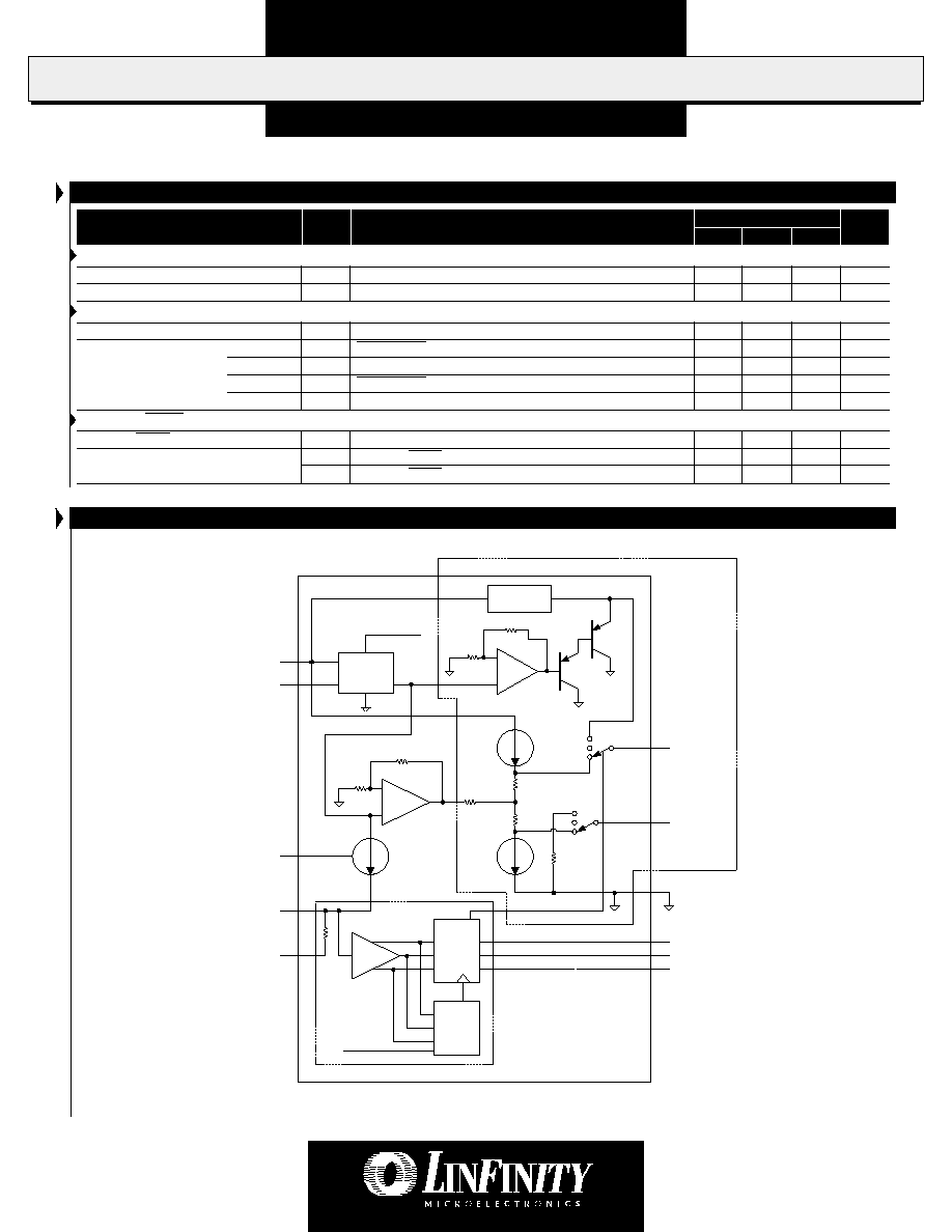
FIGURE 1 -- LX5241/5242 Block Diagram
Internal V
REF
1.30V
Power ON
S.E.
2.2V
52.5
52.5
200
Window
Comp.
LATCH
POWER
ON
&
MODE
DELAY
SE
HVD
LVD
SE
HVD
LVD
Power ON
10mA
V
TERM
DISCONNECT
M/S
DIFFSENSE
DIFFB
MODE Control & Delay
20
SE
DISC/HVD
LVD
LVD (+)
/ SE
(Pseudo-GND)
LVD (-)
/ SE
1 of 9
SE
HVD
LVD
1.07mA
1.07mA
LVD
1.25V
SE
2.85V, 22.5mA
M
U L T I M O D E
S C S I T
E R M I N A T O R
LX5241/5242/5243
P R O D U C T D A T A B O O K 1 9 9 6 / 1 9 9 7
5
Copyright © 2000
Rev. 1.4 11/00
P
R O D U C T I O N
D
A T A
S
H E E T
UltraMAX
1-, 2-, 3-, 4-, 5-, 6-, 7-, 8-, 9-6Negative signal termination lines for LVD mode. Signal termination lines for SE mode.
1+, 2+, 3+, 4+, 5+, 6+, 7+, 8+, 9+ Positive signal termination lines for LVD mode. Pseudo-ground lines for SE mode.
V
TERM
Power supply pin for terminator. Connect to SCSI bus TERMPWR. Must be decoupled by one 4.7µF
low-ESR capacitor for every three terminator devices. It is absolutely necessary to connect this pin to
the decoupling capacitor through a very low impedance (big traces on PCB). Keeping distances very
short from the decoupling capacitors to the V
TERM
pin is also critical. The value of the decoupling
capacitor is somewhat layout dependant and some applications may benefit from high-frequency
decoupling with 0.1µF capacitors right at V
TERM
pin.
DISCONNECT6Enables / disables terminator. See Power Down Function Table for logic levels per device.
GND6Terminator ground pin. Connect to ground.
MASTER / SLAVE6Sometimes referred to as M/S pin in this data sheet. Used to select which terminator is the control-
ling device. MASTER/SLAVE pin High or Open enables the DIFFSENSE output drive. Please see
MASTER/SLAVE Function Table.
DIFFSENSE6This is a dual function pin. It drives the SCSI bus DIFFSENS line. It is also the sense pin to detect the
SCSI bus mode (LVD, SE or HVD). DIFFSENSE output drive can be disabled with Low level on the
MASTER/SLAVE pin. Please see DIFFSENSE and MASTER/SLAVE Function Tables. Internally
connected to DIFFB pin through 20kOhm resistor.
DIFFB6Internally connected to DIFFSENSE pin through 20kOhm resistor. It can be used as a mode sense
pin when the device is a non-controlling terminator (MASTER/SLAVE pin is Low). An RC filter
(20kOhm / 0.1µF) is not required on the LX5241/42/43, as it has an internal timer.
SE6Single-ended output; when High, terminator is operating in SE mode.
LVD6Low Voltage Differential output. When High, terminator is operating in LVD mode.
HVD6High Voltage Differential output. When High, terminator is operating in HVD mode.
HEATSINK6Attached to die mounting pad, but not bonded to GND pin. Pins should be considered a heat sink
only, and not a true ground connection. It is recommeneded that these pins be connected to ground,
but can be left floating.
Pin
Designator Description
F U N C T I O N A L P I N D E S C R I P T I O N