D E S C R I P T I O N
K E Y F E A T U R E S
s THREE-TERMINAL ADJUSTABLE OR FIXED
OUTPUT
s GUARANTEED < 1.3V HEADROOM AT 5A
(LX8384A-xx)
s GUARANTEED 2.0% MAX. REFERENCE
TOLERANCE (LX8384A-xx)
s GUARANTEED 1.0% MAX. REFERENCE
TOLERANCE (LX8384B-xx)
s OUTPUT CURRENT OF 5A MINIMUM
p 0.015% LINE REGULATION
p 0.15% LOAD REGULATION
The LX8384/84A/84B Series ICs are posi-
tive regulators designed to provide 5A
output current. These regulators yield
higher efficiency than currently available
devices with all internal circuitry designed
to operate down to a 1V input-to-output
differential. In each of these products,
the dropout voltage is fully specified as
a function of load current. Dropout is
guaranteed at a maximum of 1.3V
(8384A) and 1.5V (8384) at maximum
output current, decreasing at lower load
currents.
In addition, on-chip trimming adjusts
the reference voltage tolerance to 1%
maximum at room temperature and 2%
maximum over the 0 to 125∞C range
for the LX8384A, making this ideal for
the Pentium P54C-VRE specification.
The LX8384B offers 0.8% tolerance at
room temperature and 1.0% maximum
over line, load and temperature.
Fixed versions are also available and
specified in the Available Options table
below.
The LX8384/84A/84B Series devices
are pin-compatible with earlier 3-
terminal regulators, such as the 117 series
products. While a 10µF output capacitor
is required on both input and output of
these new devices, this capacitor is
generally included in most regulator
designs.
The LX8384/84A/84B Series quiescent
current flows into the load, thereby
increasing efficiency. This feature
constrasts with PNP regulators where up
to 10% of the output current is wasted as
quiescent current. The LX8384-xxI is
specified over the industrial temperature
range of -25∞C to 125∞C, while the
L X 8 3 8 4 - x x C / 8 4 A - x x C / 8 4 B - x x C i s
specified over the commercial range of
0∞C to 125∞C.
A P P L I C A T I O N S
s PENTIUM
Æ
PROCESSOR VRE APPLICATIONS
s HIGH EFFICIENCY LINEAR REGULATORS
s POST REGULATORS FOR SWITCHING POWER
SUPPLIES
s BATTERY CHARGERS
s CONSTANT CURRENT REGULATORS
s CYRIX
Æ
6x86
TM
s AMD-K5
TM
5 A L
O W
D
R O P O U T
P
O S I T I V E
R
E G U L A T O R S
P
R O D U C T I O N
D
A T A
S
H E E T
T
H E
I
N F I N I T E
P
O W E R
O F
I
N N O V A T I O N
LX8384-xx/8384A-xx/8384B-xx
LIN D
O C
#: 8384
P R O D U C T H I G H L I G H T
3.5V, 5A R
E G U L AT O R
LX8384A
218
0.1%
0.1%
3.5V at 5A
*
Capacitors must
have < 20m
Total ESR.
5V
OUT
IN
ADJ
*
1500µF
6MV1500GX
Sanyo
1500µF
*
5x 6MV1500GX
Sanyo
121
Note: All surface-mount packages are available in Tape & Reel, append the letter "T" to part number.
(i.e. LX8384A-xxCDDT) "xx" refers to output voltage, please see table above.
An application of the LX8384A for the Pentium P54C processors meeting VRE specfication.
P A C K A G E O R D E R I N F O R M A T I O N
T
A
(∞C)
Plastic TO-220
3-pin
P
Plastic TO-263
3-pin
DD
2.0%
1.5V
LX8384-xxCP
LX8384-xxCDD
0 to 125
2.0%
1.3V
LX8384A-xxCP
LX8384A-xxCDD
1.0%
1.3V
LX8384B-xxCP
LX8384B-xxCDD
-25 to 125
2.0%
1.5V
LX8384-xxIP
LX8384-xxIDD
Max. Dropout
Voltage
Max. Ref.
Accuracy
LX8384/84A/84B-00
Adjustable
LX8384/84A/84B-15
1.5V
LX8384/84A/84B-33
3.3V
Part #
Output
Voltage
A
VA I L A B L E
O
P T I O N S
P E R
P
A R T
#
Other voltage options may be available --
Please contact factory for details.
Copyright © 1997
Rev. 1.9 12/97
1
11861 W
ESTERN
A
VENUE
, G
ARDEN
G
ROVE
, CA. 92841, 714-898-8121, F
AX
: 714-893-2570
L
I N
F
I N I T Y
M
I C R O E L E C T R O N I C S
I
N C
.
IMPORTANT: For the most current data, consult LinFinity's web site: http://www.linfinity.com.
5 A L
O W
D
R O P O U T
P
O S I T I V E
R
E G U L AT O R S
LX8384-xx/8384A-xx/8384B-xx
P R O D U C T D A T A B O O K 1 9 9 6 / 1 9 9 7
Copyright © 1997
Rev. 1.9 12/97
2
P
R O D U C T I O N
D
A T A
S
H E E T
ABSOLUTE MAXIMUM RATINGS
(Note 1)
Power Dissipation .................................................................................. Internally Limited
Input Voltage ................................................................................................................ 10V
Input to Output Voltage Differential ........................................................................... 10V
Operating Junction Temperature
Hermetic (K - Package) ........................................................................................ 150∞C
Plastic (DD - Package) .......................................................................................... 150∞C
Storage Temperature Range ...................................................................... -65∞C to 150∞C
Lead Temperature (Soldering, 10 seconds) ............................................................. 300∞C
PACKAGE PIN OUTS
Note 1. Exceeding these ratings could cause damage to the device. All voltages are with
respect to Ground. Currents are positive into, negative out of the specified terminal.
V
IN
V
OUT
ADJ / GND*
3
2
1
P PACKAGE
(Top View)
* Pin 1 is GND for fixed voltage versions.
3
2
1
V
IN
ADJ / GND*
V
OUT
DD PACKAGE
(Top View)
* Pin 1 is GND for fixed voltage versions.
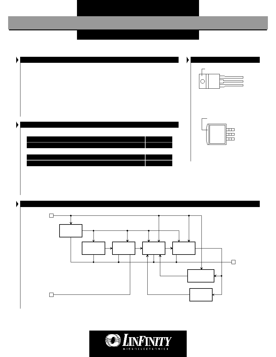
BLOCK DIAGRAM
Thermal
Limit Circuit
Control
Circuit
Bandgap
Circuit
Output
Circuit
Bias
Circuit
V
OUT
V
IN
SOA Protection
Circuit
Current
Limit Circuit
ADJ or
GND*
P PACKAGE:
THERMAL RESISTANCE-JUNCTION TO TAB,
JT
2.7∞C/W
THERMAL RESISTANCE-JUNCTION TO AMBIENT,
JA
60∞C/W
DD PACKAGE:
THERMAL RESISTANCE-JUNCTION TO TAB,
JT
2.7∞C/W
THERMAL RESISTANCE-JUNCTION TO AMBIENT,
JA
60∞C/W*
Junction Temperature Calculation: T
J
= T
A
+ (P
D
x
JA
).
The
JA
numbers are guidelines for the thermal performance of the device/pc-board system.
All of the above assume no ambient airflow.
*
JA
can be improved with package soldered to 0.5IN
2
copper area over backside ground
plane or internal power plane.
JA
can vary from 20∫C/W to > 40∫C/W depending on
mounting technique.
THERMAL DATA
TAB IS V
OUT
TAB IS V
OUT
* This pin GND for fixed voltage versions.

5 A L
O W
D
R O P O U T
P
O S I T I V E
R
E G U L A T O R S
LX8384-xx/8384A-xx/8384B-xx
P R O D U C T D A T A B O O K 1 9 9 6 / 1 9 9 7
3
Copyright © 1997
Rev. 1.9 12/97
P
R O D U C T I O N
D
A T A
S
H E E T
E L E C T R I C A L C H A R A C T E R I S T I C S
(Unless otherwise specified, these specifications apply over the operating ambient temperatures for the LX8384-xxC/8384A-xxC/8384B-xxC with
0∞C
T
A
125∞C, and the LX8384-xxI with -25∞C
T
A
125∞C; V
IN
- V
OUT
= 3V; I
OUT
= 5A. Low duty cycle pulse testing techniques are used which
maintains junction and case temperatures equal to the ambient temperature.)
Parameter
Symbol
Test Conditions
Units
LX8384/84A/84B-00
Min.
Typ.
Max.
Reference Voltage
LX8384/84A-00
V
REF
I
OUT
= 10mA, T
A
= 25∞C
(Note 4)
10mA
I
OUT
5A, 1.5V
(V
IN
- V
OUT
), V
IN
10V, P
P
MAX
LX8384B-00
I
OUT
= 10mA, T
A
= 25∞C
10mA
I
OUT
5A, 1.5V
(V
IN
- V
OUT
), V
IN
10V, P
P
MAX
Line Regulation (Note 2)
V
REF
1.3V
(V
IN
- V
OUT
), V
IN
7V, I
OUT
= 10mA
(V
IN
)
1.3V
(V
IN
- V
OUT
), V
IN
10V, I
OUT
= 10mA
Load Regulation (Note 2)
V
REF
(I
OUT
)
V
OUT
V
REF
, V
IN
- V
OUT
= 3V, 10mA
I
OUT
5A
Thermal Regulation
V
OUT
(Pwr)
T
A
= 25∞C, 20ms pulse
Ripple Rejection (Note 3)
V
OUT
= 5V, f =120Hz, C
OUT
= 100µf Tantalum, V
IN
= 6.5V
C
ADJ
= 10µF, I
OUT
= 5A
Adjust Pin Current
I
ADJ
Adjust Pin Current Change (Note 4)
I
ADJ
10mA
I
OUT
I
OUT (MAX)
, 1.3V
(V
IN
- V
OUT
), V
IN
10V
Dropout Voltage
LX8384-00
V
V
REF
= 1%, I
OUT
= 5A
LX8384A/84B-00
V
REF
= 1%, I
OUT
= 5A
Minimum Load Current
I
OUT (MIN)
V
IN
10V
Maximum Output Current
I
OUT (MAX)
(V
IN
- V
OUT
)
7V
(V
IN
- V
OUT
)
10V
Temperature Stability (Note 3)
V
OUT
(T)
Long Term Stability (Note 3)
V
OUT
(t) T
A
= 125∞C, 1000 hours
RMS Output Noise (% of V
OUT
) (Note 3) V
OUT (RMS)
T
A
= 25∞C, 10Hz
f
10kHz
1.238
1.250
1.262
V
1.225
1.250
1.270
V
1.240
1.250
1.260
V
1.238
1.250
1.262
V
0.015
0.2
%
0.035
0.3
%
0.15
0.5
%
0.01
0.02
%/W
65
83
dB
20
55
100
µA
0.2
5
µA
1.2
1.5
V
1.1
1.3
V
2
10
mA
5
6
A
3
4
A
0.25
%
0.3
1
%
0.003
%
Note 2. Regulation is measured at constant junction temperature, using pulse testing with a low duty cycle. Changes in output voltage due to
heating effects are covered under the specification for thermal regulation.
Note 3. These parameters, although guaranteed, are not tested in production.
Note 4. See Maximum Output Current Section above.
Parameter
Symbol
Test Conditions
Units
LX8384/84A/84B-15
Min.
Typ.
Max.
Output Voltage
LX8384/84A-15
V
OUT
V
IN
= 5V, I
OUT
= 0mA, T
A
= 25∞C
(Note 4)
4.75V
V
IN
10V, 0mA
I
OUT
5A, P
P
MAX
LX8384B-15
V
IN
= 5V, I
OUT
= 0mA, T
A
= 25∞C
4.75V
V
IN
10V, 0mA
I
OUT
5A, P
P
MAX
Line Regulation (Note 2)
V
OUT
4.75V
V
IN
7V
(V
IN
)
4.75V
V
IN
10V
Load Regulation (Note 2)
V
OUT
(I
OUT
)
V
IN
= 5V, 0mA
I
OUT
I
OUT (MAX)
Thermal Regulation
V
OUT
(Pwr)
T
A
= 25∞C, 20ms pulse
Ripple Rejection (Note 3)
C
OUT
= 100µF (Tantalum), I
OUT
= 5A
Quiescent Current
I
Q
0mA
I
OUT
I
OUT (MAX)
, 4.75V
V
IN
10V
Dropout Voltage
LX8384-15
V
V
OUT
= 1%, I
OUT
I
OUT (MAX)
LX8384A/84B-15
V
OUT
= 1%, I
OUT
I
OUT (MAX)
Maximum Output Current
I
OUT (MAX)
V
IN
7V
Temperature Stability (Note 3)
V
OUT
(T)
Long Term Stability (Note 3)
V
OUT
(t) T
A
= 125∞C, 1000 hours
RMS Output Noise (% of V
OUT
) (Note 3) V
OUT (RMS)
T
A
= 25∞C, 10Hz
f
10kHz
1.485
1.50
1.515
V
1.470
1.50
1.530
V
1.488
1.50
1.512
V
1.485
1.50
1.515
V
1
3
mV
1
5
mV
2.5
7
mV
0.01
0.02
% / W
60
83
dB
4
10
mA
1.2
1.5
V
1
1.3
V
5
6
A
0.25
%
0.3
1
%
0.003
%
LX8384-00 / 8384A-00 / 8384B-00 (Adjustable)
LX8384-15 / 8384A-15 / 8384B-15 (1.5V Fixed)
5 A L
O W
D
R O P O U T
P
O S I T I V E
R
E G U L AT O R S
LX8384-xx/8384A-xx/8384B-xx
P R O D U C T D A T A B O O K 1 9 9 6 / 1 9 9 7
Copyright © 1997
Rev. 1.9 12/97
4
P
R O D U C T I O N
D
A T A
S
H E E T
E L E C T R I C A L C H A R A C T E R I S T I C S
(Continued)
Parameter
Symbol
Test Conditions
Units
LX8384/84A/84B-33
Min.
Typ.
Max.
Output Voltage
LX8384/84A-33
V
OUT
V
IN
= 5V, I
OUT
= 0mA, T
A
= 25∞C
(Note 4)
4.75V
V
IN
10V, 0mA
I
OUT
5A, P
P
MAX
LX8384B-33
V
IN
= 5V, I
OUT
= 0mA, T
A
= 25∞C
4.75V
V
IN
10V, 0mA
I
OUT
5A, P
P
MAX
Line Regulation (Note 2)
V
OUT
4.75V
V
IN
7V
(V
IN
)
4.75V
V
IN
10V
Load Regulation (Note 2)
V
OUT
(I
OUT
)
V
IN
= 5V, 0mA
I
OUT
I
OUT (MAX)
Thermal Regulation
V
OUT
(Pwr)
T
A
= 25∞C, 20ms pulse
Ripple Rejection (Note 3)
C
OUT
= 100µF (Tantalum), I
OUT
= 5A
Quiescent Current
I
Q
0mA
I
OUT
I
OUT (MAX)
, 4.75V
V
IN
10V
Dropout Voltage
LX8384-33
V
V
OUT
= 1%, I
OUT
I
OUT (MAX)
LX8384A/84B-33
V
OUT
= 1%, I
OUT
I
OUT (MAX)
Maximum Output Current
I
OUT (MAX)
V
IN
7V
Temperature Stability (Note 3)
V
OUT
(T)
Long Term Stability (Note 3)
V
OUT
(t) T
A
= 125∞C, 1000 hours
RMS Output Noise (% of V
OUT
) (Note 3) V
OUT (RMS)
T
A
= 25∞C, 10Hz
f
10kHz
3.267
3.30
3.333
V
3.235
3.30
3.365
V
3.274
3.30
3.326
V
3.267
3.30
3.333
V
1
6
mV
2
10
mV
5
15
mV
0.01
0.02
% / W
60
83
dB
4
10
mA
1.2
1.5
V
1
1.3
V
5
6
A
0.25
%
0.3
1
%
0.003
%
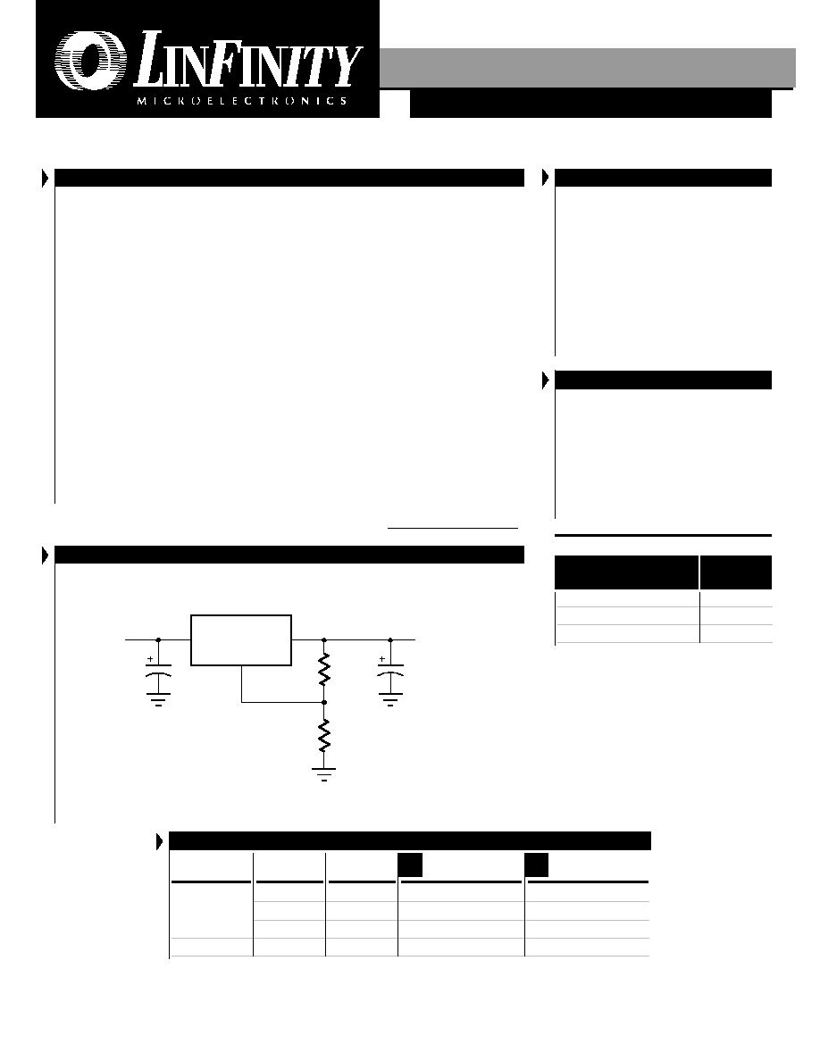
LX8384-33 / 8384A-33 / 8384B-33 (3.3V Fixed)

5 A L
O W
D
R O P O U T
P
O S I T I V E
R
E G U L A T O R S
LX8384-xx/8384A-xx/8384B-xx
P R O D U C T D A T A B O O K 1 9 9 6 / 1 9 9 7
5
Copyright © 1997
Rev. 1.9 12/97
P
R O D U C T I O N
D
A T A
S
H E E T
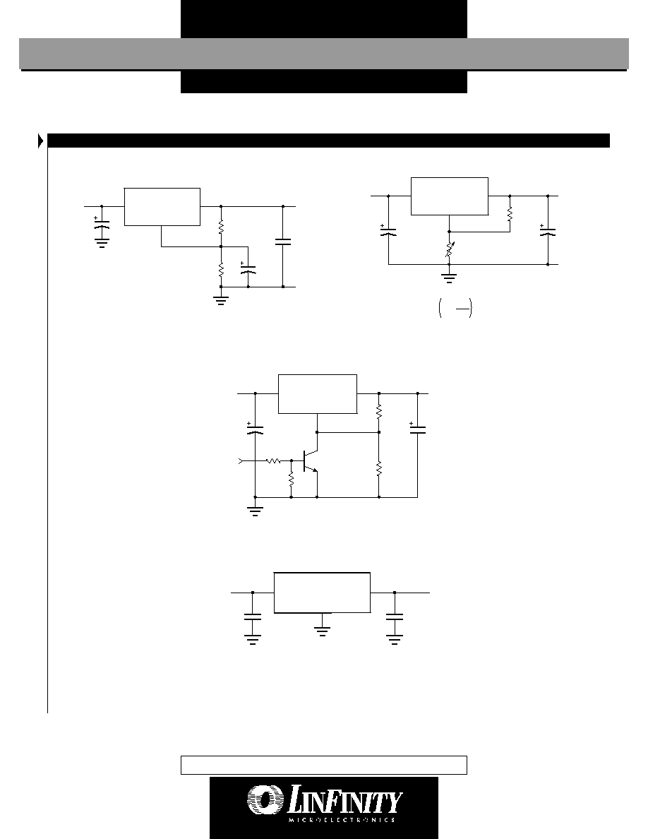
A P P L I C A T I O N N O T E S
The LX8384/84A/84B Series ICs are easy to use Low-Dropout (LDO)
voltage regulators. They have all of the standard self-protection
features expected of a voltage regulator: short circuit protection,
safe operating area protection and automatic thermal shutdown if
the device temperature rises above approximately 165∞C.
Use of an output capacitor is REQUIRED with the LX8384/84A/
84B series. Please see the table below for recommended minimum
capacitor values.
These regulators offer a more tightly controlled reference voltage
tolerance and superior reference stability when measured against
the older pin-compatible regulator types that they replace.
STABILITY
The output capacitor is part of the regulator's frequency compen-
sation system. Many types of capacitors are available, with different
capacitance value tolerances, capacitance temperature coefficients,
and equivalent series impedances. For all operating conditions,
connection of a 220µF aluminum electrolytic capacitor or a 47µF
solid tantalum capacitor between the output terminal and ground
will guarantee stable operation.
If a bypass capacitor is connected between the output voltage
adjust (ADJ) pin and ground, ripple rejection will be improved
(please see the section entitled "RIPPLE REJECTION"). When ADJ
pin bypassing is used, the required output capacitor value increases.
Output capacitor values of 220µF (aluminum) or 47µF (tantalum)
provide for all cases of bypassing the ADJ pin. If an ADJ pin bypass
capacitor is not used, smaller output capacitor values are adequate.
The table below shows recommended minimum capacitance values
for stable operation.
INPUT
OUTPUT
ADJ
10µF
15µF Tantalum, 100µF Aluminum
None
10µF
47µF Tantalum, 220µF Aluminum
15µF
To ensure good transient response from the power supply system
under rapidly changing current load conditions, designers generally
use several output capacitors connected in parallel. Such an
arrangement serves to minimize the effects of the parasitic resistance
(ESR) and inductance (ESL) that are present in all capacitors. Cost-
effective solutions that sufficiently limit ESR and ESL effects gener-
ally result in total capacitance values in the range of hundreds to
thousands of microfarads, which is more than adequate to meet
regulator output capacitor specifications. Output capacitance
values may be increased without limit.
The circuit shown in Figure 1 can be used to observe the transient
response characteristics of the regulator in a power system under
changing loads. The effects of different capacitor types and values
on transient response parameters, such as overshoot and under-
shoot, can be compared quickly in order to develop an optimum
solution.
RECOMMENDED CAPACITOR VALUES
FIGURE 1 -- DYNAMIC INPUT and OUTPUT TEST
LX8384/84A
/84B
Power Supply
OUT
IN
ADJ
Star Ground
1 sec
10ms
R
DSON
<< R
L
Full Load
(Smaller resistor)
Minumum Load
(Larger resistor)
OVERLOAD RECOVERY
Like almost all IC power regulators, the LX8384/84A/84B regulators
are equipped with Safe Operating Area (SOA) protection. The SOA
circuit limits the regulator's maximum output current to progressively
lower values as the input-to-output voltage difference increases. By
limiting the maximum output current, the SOA circuit keeps the
amount of power that is dissipated in the regulator itself within safe
limits for all values of input-to-output voltage within the operating
range of the regulator. The LX8384/84A/84B SOA protection system
is designed to be able to supply some output current for all values
of input-to-output voltage, up to the device breakdown voltage.
Under some conditions, a correctly operating SOA circuit may
prevent a power supply system from returning to regulated opera-
tion after removal of an intermittent short circuit at the output of the
regulator. This is a normal mode of operation which can be seen in
most similar products, including older devices such as 7800 series
regulators. It is most likely to occur when the power system input
voltage is relatively high and the load impedance is relatively low.
When the power system is started "cold", both the input and
output voltages are very close to zero. The output voltage closely
follows the rising input voltage, and the input-to-output voltage
difference is small. The SOA circuit therefore permits the regulator
to supply large amounts of current as needed to develop the
designed voltage level at the regulator output.
Now consider the case where the regulator is supplying regulated
voltage to a resistive load under steady state conditions. A moderate
input-to-output voltage appears across the regulator but the voltage
difference is small enough that the SOA circuitry allows sufficient
current to flow through the regulator to develop the designed output
voltage across the load resistance. If the output resistor is short-
circuited to ground, the input-to-output voltage difference across the
regulator suddenly becomes larger by the amount of voltage that had
appeared across the load resistor. The SOA circuit reads the
increased input-to-output voltage, and cuts back the amount of
current that it will permit the regulator to supply to its output
terminal. When the short circuit across the output resistor is
removed, all the regulator output current will again flow through the
output resistor. The maximum current that the regulator can supply
to the resistor will be limited by the SOA circuit, based on the large
input-to-output voltage across the regulator at the time the short
circuit is removed from the output. If this limited current is not
sufficient to develop the designed voltage across the output resistor,

5 A L
O W
D
R O P O U T
P
O S I T I V E
R
E G U L AT O R S
LX8384-xx/8384A-xx/8384B-xx
P R O D U C T D A T A B O O K 1 9 9 6 / 1 9 9 7
Copyright © 1997
Rev. 1.9 12/97
6
P
R O D U C T I O N
D
A T A
S
H E E T
A P P L I C A T I O N N O T E S
FIGURE 2 -- BASIC ADJUSTABLE REGULATOR
R2+R1
R1
LX8384/84A/84B
OUT
IN
ADJ
V
OUT
V
IN
R1
R2
V
REF
I
ADJ
50µA
V
OUT
= V
REF
1 + + I
ADJ
R2
R2
R1
OVERLOAD RECOVERY (continued)
the voltage will stabilize at some lower value, and will never reach
the designed value. Under these circumstances, it may be necessary
to cycle the input voltage down to zero in order to make the
regulator output voltage return to regulation.
RIPPLE REJECTION
Ripple rejection can be improved by connecting a capacitor
between the ADJ pin and ground. The value of the capacitor should
be chosen so that the impedance of the capacitor is equal in
magnitude to the resistance of R1 at the ripple frequency. The
capacitor value can be determined by using this equation:
C = 1 / (6.28 * F
R
* R1)
where: C
the value of the capacitor in Farads;
select an equal or larger standard value.
F
R
the ripple frequency in Hz
R1
the value of resistor R1 in ohms
At a ripple frequency of 120Hz, with R1 = 100
:
C = 1 / (6.28 * 120Hz * 100
) = 13.3µF
The closest equal or larger standard value should be used, in this
case, 15µF.
When an ADJ pin bypass capacitor is used, output ripple
amplitude will be essentially independent of the output voltage. If
an ADJ pin bypass capacitor is not used, output ripple will be
proportional to the ratio of the output voltage to the reference
voltage:
M = V
OUT
/V
REF
where: M
a multiplier for the ripple seen when the
ADJ pin is optimally bypassed.
V
REF
= 1.25V.
For example, if V
OUT
= 2.5V the output ripple will be:
M = 2.5V/1.25V= 2
Output ripple will be twice as bad as it would be if the ADJ pin
were to be bypassed to ground with a properly selected capacitor.
OUTPUT VOLTAGE
The LX8384/84A/84B ICs develop a 1.25V reference voltage
between the output and the adjust terminal (See Figure 2). By
placing a resistor, R1, between these two terminals, a constant
current is caused to flow through R1 and down through R2 to set
the overall output voltage. Normally this current is the specified
minimum load current of 10mA. Because I
ADJ
is very small and
constant when compared with the current through R1, it represents
a small error and can usually be ignored.
LOAD REGULATION
Because the LX8384/84A/84B regulators are three-terminal devices,
it is not possible to provide true remote load sensing. Load
regulation will be limited by the resistance of the wire connecting
the regulator to the load. The data sheet specification for load
regulation is measured at the bottom of the package. Negative side
sensing is a true Kelvin connection, with the bottom of the output
divider returned to the negative side of the load. Although it may
not be immediately obvious, best load regulation is obtained when
the top of the resistor divider, (R1), is connected directly to the case
of the regulator, not to the load. This is illustrated in Figure 3. If R1
were connected to the load, the effective resistance between the
regulator and the load would be:
R
Peff
= R
P
*
where: R
P
Actual parasitic line resistance.
When the circuit is connected as shown in Figure 3, the parasitic
resistance appears as its actual value, rather than the higher R
Peff
.
LX8384/84A/84B
OUT
IN
ADJ
V
IN
R1
R2
R
L
R
P
Parasitic
Line Resistance
Connect
R2
to Load
Connect
R1 to Case
of Regulator
FIGURE 3 -- CONNECTIONS FOR BEST LOAD REGULATION
5 A L
O W
D
R O P O U T
P
O S I T I V E
R
E G U L A T O R S
LX8384-xx/8384A-xx/8384B-xx
P R O D U C T D A T A B O O K 1 9 9 6 / 1 9 9 7
7
Copyright © 1997
Rev. 1.9 12/97
P
R O D U C T I O N
D
A T A
S
H E E T
A P P L I C A T I O N N O T E S
Example
Given: V
IN
= 5V
V
OUT
= 2.8V, I
OUT
= 5.0A
Ambient Temp., T
A
= 50∞C
R
JT
= 2.7∞C/W for TO-220
300 ft/min airflow available
Find: Proper Heat Sink to keep IC's junction
temperature below 125∞C.**
Solution: The junction temperature is:
T
J
= P
D
(R
JT
+ R
CS
+ R
SA
) + T
A
where: P
D
Dissipated power.
R
JT
Thermal resistance from the junction to the
mounting tab of the package.
R
CS
Thermal resistance through the interface
between the IC and the surface on which
it is mounted. (1.0∞C/W at 6 in-lbs
mounting screw torque.)
R
SA
Thermal resistance from the mounting surface
to ambient (thermal resistance of the heat sink).
T
S
Heat sink temperature.
First, find the maximum allowable thermal resistance of the
heat sink:
R
SA
=
- (R
JT
+ R
CS
)
P
D
= (V
IN(MAX)
- V
OUT
) I
OUT
= (5.0V-2.8V) * 5.0A
= 11.0W
R
SA
=
- (2.7∞C/W
+ 1.0∞C/W)
= 3.1∞C/W
Next, select a suitable heat sink. The selected heat sink must have
R
SA
3.1∞C/W. Thermalloy heatsink 6296B has R
SA
= 3.0∞C/W with
300ft/min air flow.
Finally, verify that junction temperature remains within speci-
fication using the selected heat sink:
T
J
= 11W (2.7∞C/W + 1.0∞C/W + 3.0∞C/W) + 50∞C = 124∞C
T
J
T
C
T
S
T
A
R
JT
R
CS
R
SA
T
J
- T
A
P
D
125∞C - 50∞C
(5.0V-2.8V) * 5.0A
**
Although the device can operate up to 150∞C junction, it is recom-
mended for long term reliability to keep the junction temperature
below 125∞C whenever possible.
LOAD REGULATION (continued)
Even when the circuit is configured optimally, parasitic resistance
can be a significant source of error. A 100 mil wide PC trace built
from 1 oz. copper-clad circuit board material has a parasitic
resistance of about 5 milliohms per inch of its length at room
temperature. If a 3-terminal regulator used to supply 2.50 volts is
connected by 2 inches of this trace to a load which draws 5 amps
of current, a 50 millivolt drop will appear between the regulator and
the load. Even when the regulator output voltage is precisely
2.50 volts, the load will only see 2.45 volts, which is a 2% error. It
is important to keep the connection between the regulator output
pin and the load as short as possible, and to use wide traces or
heavy-gauge wire.
The minimum specified output capacitance for the regulator
should be located near the reglator package. If several capacitors
are used in parallel to construct the power system output capaci-
tance, any capacitors beyond the minimum needed to meet the
specified requirements of the regulator should be located near the
sections of the load that require rapidly-changing amounts of
current. Placing capacitors near the sources of load transients will
help ensure that power system transient response is not impaired
by the effects of trace impedance.
To maintain good load regulation, wide traces should be used on
the input side of the regulator, especially between the input
capacitors and the regulator. Input capacitor ESR must be small
enough that the voltage at the input pin does not drop below V
IN (MIN)
during transients.
V
IN (MIN)
= V
OUT
+ V
DROPOUT (MAX)
where: V
IN (MIN)
the lowest allowable instantaneous
voltage at the input pin.
V
OUT
the designed output voltage for the
power supply system.
V
DROPOUT (MAX)
the specified dropout voltage
for the installed regulator.
THERMAL CONSIDERATIONS
The LX8384/84A/84B regulators have internal power and thermal
limiting circuitry designed to protect each device under overload
conditions. For continuous normal load conditions, however,
maximum junction temperature ratings must not be exceeded. It is
important to give careful consideration to all sources of thermal
resistance from junction to ambient. This includes junction to case,
case to heat sink interface, and heat sink thermal resistance itself.
Junction-to-case thermal resistance is specified from the IC
junction to the back surface of the case directly opposite the die.
This is the lowest resistance path for heat flow. Proper mounting
is required to ensure the best possible thermal flow from this area
of the package to the heat sink. Thermal compound at the case-to-
heat-sink interface is strongly recommended. If the case of the
device must be electrically isolated, a thermally conductive spacer
can be used, as long as its added contribution to thermal resistance
is considered. Note that the case of all devices in this series is
electrically connected to the output.
5 A L
O W
D
R O P O U T
P
O S I T I V E
R
E G U L AT O R S
LX8384-xx/8384A-xx/8384B-xx
P R O D U C T D A T A B O O K 1 9 9 6 / 1 9 9 7
Copyright © 1997
Rev. 1.9 12/97
8
P
R O D U C T I O N
D
A T A
S
H E E T
T Y P I C A L A P P L I C A T I O N S
LX8384/84A/84B
OUT
IN
ADJ
150µF
V
IN
R2
365
1%
10µF
R1
121
1%
C1
10µF*
* C1 improves ripple rejection.
X
C
should be
R1 at ripple
frequency.
V
OUT
5V
(Note A)
FIGURE 5 -- 1.2V - 8V ADJUSTABLE REGULATOR
FIGURE 4 -- IMPROVING RIPPLE REJECTION
LX8384/84A/84B
OUT
IN
ADJ
V
OUT
**
V
IN
R1
121
R2
1k
C1*
10µF
* Needed if device is far from filter capacitors.
** V
OUT
= 1.25V 1 +
C2
100µF
R2
R1
(Note A)
FIGURE 6 -- 5V REGULATOR WITH SHUTDOWN
LX8384/84A/84B
OUT
IN
ADJ
5V
V
IN
121
1%
10µF
100µF
365
1%
1k
1k
2N3904
TTL
Output
(Note A)
Note A: V
IN (MIN)
= (Intended V
OUT
) + (V
DROPOUT (MAX)
)
Pentium is a registered trademark of Intel Corporation.
Cyrix is a registered trademark and 6x86 is a trademark of Cyrix Corporation. K5 is a trademark of AMD.
FIGURE 7 -- FIXED 3.3V OUTPUT REGULATOR
3.3V
V
IN
10µF Tantalum
or 100µF Aluminum
Min. 15µF Tantalum or
100µF Aluminum capacitor.
May be increased without
limit. ESR must be less
than 50m
.
LX8384/84A/84B-33
OUT
IN
GND
PRODUCTION DATA - Information contained in this document is proprietary to Linfinity, and is current as of publication date. This document
may not be modified in any way without the express written consent of Linfinity. Product processing does not necessarily include testing of
all parameters. Linfinity reserves the right to change the configuration and performance of the product and to discontinue product at any time.