 | –≠–ª–µ–∫—Ç—Ä–æ–Ω–Ω—ã–π –∫–æ–º–ø–æ–Ω–µ–Ω—Ç: LX8941 | –°–∫–∞—á–∞—Ç—å:  PDF PDF  ZIP ZIP |

D E S C R I P T I O N
K E Y F E A T U R E S
s
s
s
s
s 2% Internally Trimmed Output
s
s
s
s
s Output Current In Excess Of 1A
s
s
s
s
s Input-Output Differential
Less Than 0.8V At 1A
p Reverse Battery Protection
p Short Circuit Protection
p Internal Thermal Overload Protection
p Available In 5-Lead Plastic TO-220 And
Surface-Mount TO-263
The LX8941 is an adjustable, low
dropout regulator rated for more than
1A of output current. It can regulate
with as low as 0.8V headroom between
the input and output voltages, at 1A
output current, thus minimizing power
dissipation. In addition, it can be used
in applications where worst case
supplies require a low input-output
differential to maintain regulation. This
feature makes it ideal for some
processor applications that require 4V
operation from a 5V supply. In
addition, the LX8941 provides an on/off
switch that reduces the IC quiescent
current when activated, making it ideal
for battery operated applications.
P R O D U C T H I G H L I G H T
PA C K A G E O R D E R I N F O R M A T I O N
T
A
(∞C)
0 to 70
LX8941CP
LX8941CDD
Plastic TO-220
5-pin
P
Plastic TO-263
5-pin
DD
5V
4V
22µF
ADJ
OUT
LX8941
ON
OFF
10µF
IN
D
R O P O U T
V
O LTA G E
V S
. O
U T P U T
C
U R R E N T
V S
. T
E M P E R AT U R E
100
0
Output Current - (mA)
600
Dropout Voltage - (mV)
200
100
500
1000
400
500
300
125∞C
25∞C
-40∞C
A
D J U S T A B L E
L
O W
D
R O P O U T
R
E G U L A T O R
P
R E L I M I N A R Y
D
A T A
S
H E E T
T
H E
I
N F I N I T E
P
O W E R
O F
I
N N O V A T I O N
LX8941
LIN D
O C
#: 8941
Note: All surface-mount packages are available in Tape & Reel.
Append the letter "T" to part number. (i.e. LX8941CDDT)
Copyright © 1999
Rev. 0.6 4/99
1
11861 W
ESTERN
A
VENUE
, G
ARDEN
G
ROVE
, CA. 92841, 714-898-8121, F
AX
: 714-893-2570
L
I N
F
I N I T Y
M
I C R O E L E C T R O N I C S
I
N C
.
NOTE: For current data & package dimensions, visit our web site: http://www.linfinity.com.
A
D J U S T A B L E
L
O W
D
R O P O U T
R
E G U L A T O R
LX8941
P R O D U C T D A T A B O O K 1 9 9 6 / 1 9 9 7
Copyright © 1999
Rev. 0.6 4/99
2
P
R E L I M I N A R Y
D
A T A
S
H E E T
ABSOLUTE MAXIMUM RATINGS
(Note 1)
Input Voltage (V
IN
) ....................................................................................................... 26V
Operating Junction Temperature
Plastic (P, DD Package) ........................................................................................ 150∞C
Storage Temperature Range ...................................................................... -65∞C to 150∞C
Lead Temperature (Soldering, 10 seconds) ............................................................. 300∞C
PACKAGE PIN OUTS
Note 1. Exceeding these ratings could cause damage to the device. All voltages are with respect
to Ground. Currents are positive into, negative out of the specified terminal.
P PACKAGE:
THERMAL RESISTANCE-JUNCTION TO TAB,
JT
4.5∞C/W
THERMAL RESISTANCE-JUNCTION TO AMBIENT,
JA
60∞C/W
DD PACKAGE:
THERMAL RESISTANCE-JUNCTION TO TAB,
JT
4.5∞C/W
THERMAL RESISTANCE-JUNCTION TO AMBIENT,
JA
60∞C/W
Junction Temperature Calculation: T
J
= T
A
+ (P
D
x
JA
).
The
JA
numbers are guidelines for the thermal performance of the device/pc-board system.
All of the above assume no ambient airflow.
THERMAL DATA
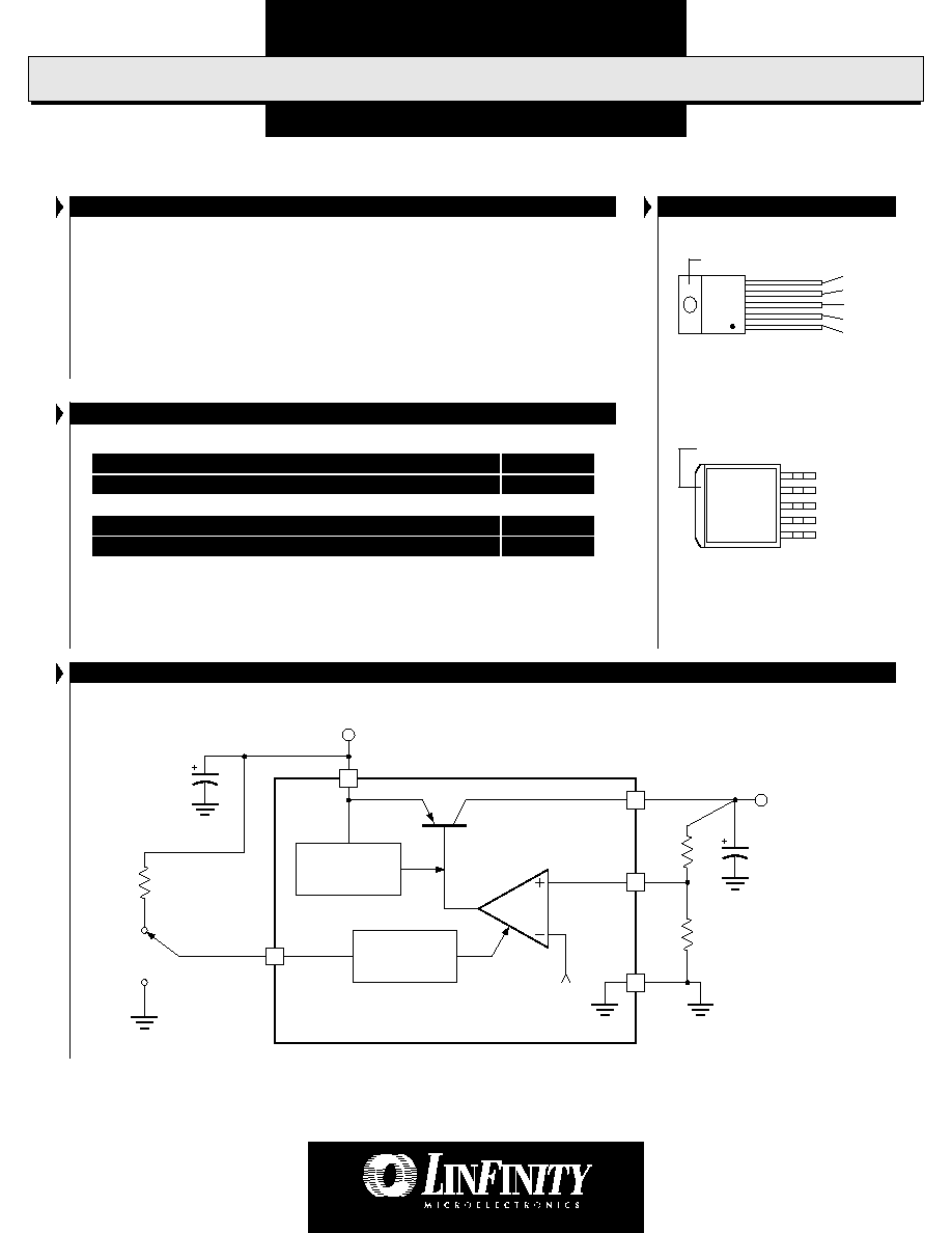
BLOCK DIAGRAM
* Required if regulator is located far from power supply
filter.
INPUT VOLTAGE
THERMAL
SHUTDOWN
ON/
OFF
ON
OFF
5
ON/OFF
CIRCUIT
GND
3
4
2
ADJ
V
O
1
V
IN
OUTPUT
VOLTAGE
C1*
0.1µF
C2
10µF
LX8941
ON/OFF
ADJ
GND
V
O
V
IN
P PACKAGE
(Top View)
1
5
DD PACKAGE
(Top View)
ON/OFF
ADJ
GND
V
O
V
IN
3
2
1
4
5
TAB IS GND
TAB IS GND

A
D J U S T A B L E
L
O W
D
R O P O U T
R
E G U L A T O R
LX8941
P R O D U C T D A T A B O O K 1 9 9 6 / 1 9 9 7
3
Copyright © 1999
Rev. 0.6 4/99
P
R E L I M I N A R Y
D
A T A
S
H E E T
Input Voltage (Note 2)
V
IN
Load Current (with adequate heatsinking)
Input Capacitor (V
IN
to GND)
Output Capacitor with ESR of 10
max., (V
OUT
to GND)
R E C O M M E N D E D O P E R A T I N G C O N D I T I O N S
Parameter
Symbol
Units
Recommended Operating Conditions
Min.
Typ.
Max.
3.8
26
V
5
1000
mA
0.1
µF
10
µF
E L E C T R I C A L C H A R A C T E R I S T I C S
Unless otherwise specified, these specifications apply over the operating ambient temperature of 0∞C to +125∞C for LX8941CP; V
IN
= 10V, I
O
= 1A, C
OUT
= 22µF, and are for DC characteristics only. (Low duty cycle pulse testing techniques are used which maintains junction and case temperatures equal
to the ambient temperature.)
Parameter
Symbol
Test Conditions
Units
ADJ Pin Voltage
V
O
I
O
= 0A, T
A
= 25∫C
Line Regulation
V
OI
V
O
+ 2V
V
IN
26V, I
O
= 5mA
Load Regulation
V
OL
50mA
I
O
1A, V
O
= V
ADJ
Dropout Voltage
V
I
O
= 100mA
I
O
= 500mA
I
O
= 1A
Quiescent Current
I
Q
I
O
5mA, 7
V
IN
26V
I
O
= 500mA
I
O
= 1000mA
Adjust Pin Current
I
ADJ
V
IN
= 10V, I
O
= 1A
Current Limit
I
CL
V
IN
= 26V
Output Noise Voltage (Note 3)
V
O RMS
10Hz - 100kHz, I
O
= 5mA
Long Term Stability (Note 3)
Ripple Rejection (Note 3)
R
R
f
O
= 120Hz, 1V
RMS
, I
O
= 100mA
LX8941
Min.
Typ.
Max.
Note 2. V
IN (MIN)
= V
OUT
+ 1.2
V
(MAX)
. See Dropout Voltage maximum limit.
1.225
1.25
1.275
V
1
50
mV
10
50
mV
150
300
mV
275
500
mV
400
800
mV
3
15
mA
30
50
mA
115
180
mA
2
20
µA
1
1.2
A
150
µV
RMS
20
mV/1000hr
66
dB
Note 3. These parameters, although guaranteed, are not tested in production.
On Threshold Voltage
On Threshold Current
Off Threshold Voltage
Off Threshold Current
Enable Logic Section
2
V
50
µA
0.8
V
-10
µA
PRELIMINARY DATA - Information contained in this document is pre-production data, and is proprietary to LinFinity. It may
not modified in any way without the express written consent of LinFinity. Product referred to herein is offered in sample form
only, and Linfinity reserves the right to change or discontinue this proposed product at any time.