NESG2021M05
NEC's NPN SiGe
HIGH FREQUENCY TRANSISTOR
M05
DESCRIPTION
NEC's NESG2021M05 is fabricated using NECs high voltage
Silicon Germanium process (UHS2-HV), and is designed for
a wide range of applications including low noise amplifiers,
medium power amplifiers, and oscillators.
NECs low profile, flat lead style M05 Package provides high
frequency performance for compact wireless designs.
California Eastern Laboratories
∑
HIGH BREAKDOWN VOLTAGE SiGe TECHNOLOGY
V
CEO
= 5 V (Absolute Maximum)
∑
LOW NOISE FIGURE:
NF
= 0.9 dB at 2 GHz
NF
= 1.3 dB at 5.2 GHz
∑ HIGH MAXIMUM STABLE GAIN:
MSG
= 22.5 dB at 2 GHz
∑
LOW PROFILE M05 PACKAGE:
SOT-343 footprint, with a height of only 0.59 mm
Flat lead style for better RF performance
∑
Pb Free
FEATURES
Notes:
1. MSG =
2. Collector to base capacitance is measured by capacitance meter (automatic balance bridge method) when emitter pin is connected to
the guard pin.
3. Pulsed measurement, pulse width 350 s, duty cycle 2 %.
S
21
S
12
DATA SHEET
PART NUMBER
NESG2021M05
PACKAGE OUTLINE
M05
SYMBOLS
PARAMETERS AND CONDITIONS
UNITS
MIN
TYP
MAX
NF
Noise Figure at V
CE
= 2 V, I
C
= 3 mA, f = 5.2 GHz,
dB
1.3
Z
S
= Z
SOPT
, ZL = Z
LOPT
G
a
Associated Gain at V
CE
= 2 V, I
C
= 3 mA, f = 5.2 GHz,
dB
10.0
Z
S
= Z
SOPT
, ZL = Z
LOPT
NF
Noise Figure at V
CE
= 2 V, I
C
= 3 mA, f = 2 GHz,
dB
0.9
1.2
Z
S
= Z
SOPT
, ZL = Z
LOPT
G
a
Associated Gain at V
CE
= 2 V, I
C
= 3 mA, f = 2 GHz,
dB
15.0
18.0
Z
S
= Z
SOPT
, ZL = Z
LOPT
MSG
Maximum Stable Gain
1
at V
CE
= 3 V, I
C
= 10 mA, f = 2 GHz
dB
20.0
22.5
|S
21E
|
2
Insertion Power Gain at V
CE
= 3 V, I
C
= 10 mA, f = 2 GHz
dB
17.0
19.0
P
1dB
Output Power at 1dB Compression Point at
dBm
9.0
V
CE
= 3 V, I
C
= 12 mA, f = 2 GHz
OIP
3
Output 3rd Order Intercept Point at V
CE
= 3 V, I
C
= 12 mA, f = 2 GHz dBm
17.0
f
T
Gain Bandwidth Product at V
CE
= 3 V, I
C
= 10 mA, f = 2 GHz
GHz
20
25
C
re
Reverse Transfer Capacitance
2
at V
CB
= 2 V, I
C
= 0 mA, f = 1 GHz
pF
0.1
0.2
I
CBO
Collector Cutoff Current at V
CB
= 5V, I
E
= 0
nA
100
I
EBO
Emitter Cutoff Current at V
EB
= 1 V, I
C
= 0
nA
100
h
FE
DC Current Gain
3
at V
CE
= 2 V, I
C
= 5 mA
130
190
260
ELECTRICAL CHARACTERISTICS
(T
A
= 25∞C)
DC
RF

Note:
1. Operation in excess of any one of these parameters may result
in permanent damage.
2. Mounted on 1.08 cm
2
x 1.0 mm (t) glass epoxy PCB.
SYMBOLS
PARAMETERS
UNITS
RATINGS
V
CBO
Collector to Base Voltage
V
13.0
V
CEO
Collector to Emitter Voltage
V
5.0
V
EBO
Emitter to Base Voltage
V
1.5
I
C
Collector Current
mA
35
P
T
2
Total Power Dissipation
mW
175
T
J
Junction Temperature
∞C
150
T
STG
Storage Temperature
∞C
-65 to +150
ABSOLUTE MAXIMUM RATINGS
1
(T
A
= 25∞C)
SYMBOLS
PARAMETERS
UNITS
RATINGS
R
th j-c
Junction to Case Resistance ∞C/W
TBD
THERMAL RESISTANCE
NESG2021M05
ORDERING INFORMATION
Collector to Base Voltage, V
CB
(V)
Reverse
T
ransfer Capacitance, C
re
(pF)
TYPICAL PERFORMANCE CURVES
(T
A
= 25∞C)
Base to Emitter Voltage, V
BE
(V)
Collector Current, Ic (mA)
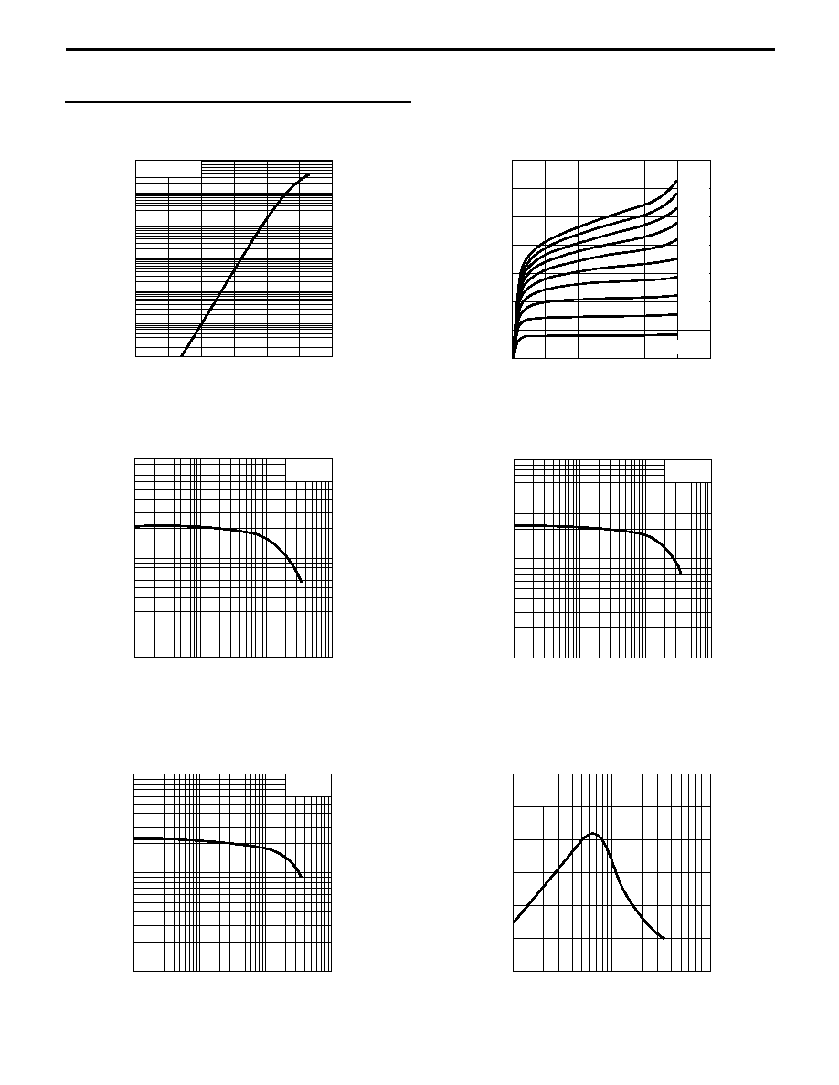
COLLECTOR CURRENT vs.
BASE TO EMITTER VOLTAGE
REVERSE TRANSFER CAPACITANCE
vs. COLLECTOR TO BASE VOLTAGE
Ambient Temperature, T
A
(∞C)
T
otal Power Dissipation, P
tot
(mW)
TOTAL POWER DISSIPATION vs.
AMBIENT TEMPERATURE
Base to Emitter Voltage, V
BE
(V)
Collector Current, Ic (mA)
COLLECTOR CURRENT vs.
BASE TO EMITTER VOLTAGE
Mounted on Glass Epoxy PCB
(1.08 cm
2
◊ 1.0 mm (t) )
250
200
150
175
100
50
0
25
50
75
100
125
150
f = 1 MHz
0.3
0.2
0.1
0
2
4
6
8
10
V
CE
= 1 V
100
10
1
0.01
0.001
0.1
0.0001
0.7
0.5
0.6
0.4
0.8
0.9
1.0
V
CE
= 2 V
100
10
1
0.01
0.001
0.1
0.0001
0.7
0.5
0.6
0.4
0.8
0.9
1.0
PART NUMBER
QUANTITY
SUPPLYING FORM
NESG2021M05-T1-A 3 kpcs/reel ∑ Pb Free
∑ Pin 3 (Collector), Pin 4
(Emitter) face the perforation
side of the tape
∑ 8 mm wide embossed taping
NESG2021M05
Collector to Emitter Voltage, V
CE
(V)
Collector Current, Ic (mA)
TYPICAL PERFORMANCE CURVES
(T
A
= 25∞C)
Collector Current, l
C
(mA)
DC Current Gain, h
FE
DC CURRENT GAIN vs.
COLLECTOR CURRENT
COLLECTOR CURRENT vs.
COLLECTOR TO EMITTER VOLTAGE
Base to Emitter Voltage, V
BE
(V)
Collector Current, Ic (mA)
COLLECTOR CURRENT vs.
BASE TO EMITTER VOLTAGE
Collector Current, l
C
(mA)
DC Current Gain, h
FE
DC CURRENT GAIN vs.
COLLECTOR CURRENT
Collector Current, l
C
(mA)
DC Current Gain, h
FE
DC CURRENT GAIN vs.
COLLECTOR CURRENT
Collector Current, l
C
(mA)
Gain Bandwidth Product, f
T
(GHz)
GAIN BANDWIDTH PRODUCT
vs. COLLECTOR CURRENT
V
CE
= 3 V
100
10
1
0.01
0.001
0.1
0.0001
0.7
0.5
0.6
0.4
0.8
0.9
1.0
35
20
25
30
15
5
10
0
1
2
3
4
5
6
I
B
= 20 A
µ
120 A
µ
200 A
µ
140 A
µ
160 A
µ
180 A
µ
80 A
µ
60 A
µ
40 A
µ
100 A
µ
1 000
100
10
1
0.1
10
100
V
CE
= 1 V
1 000
100
10
1
0.1
10
100
V
CE
= 2 V
1 000
100
10
1
0.1
10
100
V
CE
= 3 V
V
CE
= 1 V
f = 2 GHz
30
5
10
15
20
25
0
10
1
100

NESG2021M05
TYPICAL PERFORMANCE CURVES
(T
A
= 25∞C)
Frequency, f (GHz)
Collector Current, I
C
(mA)
Insertion Power Gain, IS
21e
I
2
(dB)
Maximum
A
vailable Gain, MAG (dB)
Maximum Stable Power Gain, MSG (dB)
Insertion Power Gain, IS
21e
I
2
(dB)
Maximum
A
vailable Gain, MAG (dB)
Maximum Stable Power Gain, MSG (dB)
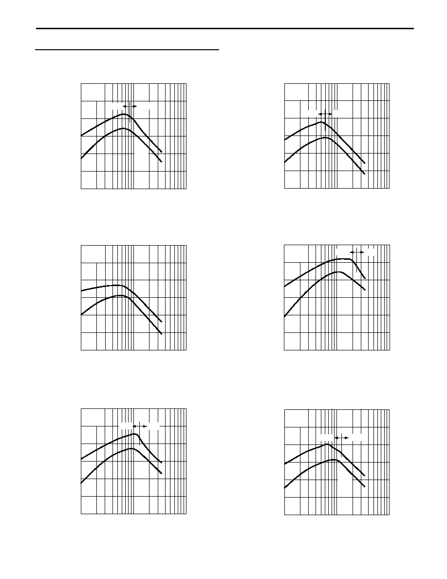
INSERTION POWER GAIN, MAG, MSG
vs. FREQUENCY
INSERTION POWER GAIN, MAG, MSG
vs. COLLECTOR CURRENT
Frequency, f (GHz)
Insertion Power Gain, IS
21e
I
2
(dB)
Maximum
A
vailable Gain, MAG (dB)
Maximum Stable Power Gain, MSG (dB)
INSERTION POWER GAIN, MAG, MSG
vs. FREQUENCY
Frequency, f (GHz)
Insertion Power Gain, IS
21e
I
2
(dB)
Maximum
A
vailable Gain, MAG (dB)
Maximum Stable Power Gain, MSG (dB)
INSERTION POWER GAIN, MAG,
MSG vs. FREQUENCY
Collector Current, l
C
(mA)
Gain Bandwidth Product, f
T
(GHz)
GAIN BANDWIDTH PRODUCT
vs. COLLECTOR CURRENT
Collector Current, l
C
(mA)
Gain Bandwidth Product, f
T
(GHz)
GAIN BANDWIDTH PRODUCT
vs. COLLECTOR CURRENT
V
CE
= 2 V
f = 2 GHz
30
5
10
15
20
25
0
10
1
100
V
CE
= 3 V
f = 2 GHz
30
5
10
15
20
25
0
10
1
100
V
CE =
1 V
I
C
= 10 mA
40
35
30
25
20
15
10
5
0
0.1
1
10
100
MAG
MSG
|S
21e
|
2
V
CE
= 2 V
I
C
= 10 mA
40
35
30
25
20
15
10
5
0
0.1
1
10
100
MAG
MSG
|S
21e
|
2
V
CE
= 3 V
I
C
= 10 mA
40
35
30
25
20
15
10
5
0
0.1
1
10
100
MAG
MSG
|S
21e
|
2
V
CE
= 1 V
f = 1 GHz
30
25
20
15
10
5
0
1
10
100
MAG
MSG
|S
21e
|
2
NESG2021M05
Collector Current, I
C
(mA)
Insertion Power Gain, IS
21e
I
2
(dB)
Maximum
A
vailable Gain, MAG (dB)
Maximum Stable Power Gain, MSG (dB)
INSERTION POWER GAIN, MAG, MSG
vs. COLLECTOR CURRENT
INSERTION POWER GAIN, MAG, MSG
vs. COLLECTOR CURRENT
Collector Current, I
C
(mA)
Insertion Power Gain, IS
21e
I
2
(dB)
Maximum
A
vailable Gain, MAG (dB)
Maximum Stable Power Gain, MSG (dB)
TYPICAL PERFORMANCE CURVES
(T
A
= 25∞C)
Collector Current, I
C
(mA)
Insertion Power Gain, IS
21e
I
2
(dB)
Maximum
A
vailable Gain, MAG (dB)
Maximum Stable Power Gain, MSG (dB)
INSERTION POWER GAIN, MAG, MSG
vs. COLLECTOR CURRENT
Collector Current, I
C
(mA)
Insertion Power Gain, IS
21e
I
2
(dB)
Maximum
A
vailable Gain, MAG (dB)
Maximum Stable Power Gain, MSG (dB)
INSERTION POWER GAIN, MAG, MSG
vs. COLLECTOR CURRENT
Collector Current, I
C
(mA)
Insertion Power Gain, IS
21e
I
2
(dB)
Maximum
A
vailable Gain, MAG (dB)
Maximum Stable Power Gain, MSG (dB)
INSERTION POWER GAIN, MAG, MSG
vs. COLLECTOR CURRENT
Collector Current, I
C
(mA)
Insertion Power Gain, IS
21e
I
2
(dB)
Maximum
A
vailable Gain, MAG (dB)
Maximum Stable Power Gain, MSG (dB)
INSERTION POWER GAIN, MAG, MSG
vs. COLLECTOR CURRENT
V
CE
= 1 V
f = 2 GHz
30
25
20
15
10
5
0
1
10
100
MAG
MSG
|S
21e
|
2
V
CE
= 1 V
f = 3 GHz
30
25
20
15
10
5
0
1
10
100
MAG
MSG
|S
21e
|
2
V
CE
= 1 V
f = 5 GHz
25
20
15
10
5
0
-5
1
10
100
|S
21e
|
2
MAG
V
CE
= 2 V
f = 1 GHz
30
25
20
15
10
5
0
1
10
100
MAG
MSG
|S
21e
|
2
V
CE
= 2 V
f = 2 GHz
30
25
20
15
10
5
0
1
10
100
MAG
MSG
|S
21e
|
2
V
CE
= 2 V
f = 3 GHz
30
25
20
15
10
5
0
1
10
100
MAG
MSG
|S
21e
|
2