
DS2429 - 3.2 September 1994
NJ88C33
Frequency Synthesiser (I
2
C BUS Programmable)
Advance Information
Fig.2 Simplified block diagram of NJ88C33
The NJ88C33 is a synthesiser circuit fabricated on Mitel
Semiconductor's 1.4 micron CMOS process, assuring very
high performance. It is I
2
C compatible and can also be
programmed at up to 5MHz. It contains a 16-bit R counter, a
12-bit N counter and a 7-bit A counter.
A digital phase comparator gives improved loop stability
with current source outputs to reduce loop components. A
voltage doubler is provided for the loop driver to improve
control voltage range to the VCO when operating at low supply
voltages.
FEATURES
s
Easy to Use
s
Low Power Consumption (15mW)
s
Single Supply 2.5V to 5.5V
s
Digital Phase Comparator with Current Source
Outputs
s
Serial (I
2
C Compatible) Programming, 5MHz max
s
Channel Loading in 8�s
s
150MHz Input Frequency Without Prescaler at 4.5V
(52MHz at 2.7V)
s
Standby Modes
s
Use of Two-Modulus Prescaler is Possible
APPLICATIONS
s
Cordless Telephones (CT2, DECT)
s
Cellular Telephones (GSM, PCN, ETACS)
s
Hand Held Marine Radios
s
Sonarbuoys
s
Video Clock generators
ABSOLUTE MAXIMUM RATINGS
Supply voltage, V
DD
-0.3V to 7V
Input voltage, V
IM1
-0.3 to V
DD
+0.3V
Output voltage on pin 13, V
IM2
-V
DD
to 0V
Storage temperature, T
stg
-55�C to +125�C
ORDERING INFORMATION
NJ88C33 MA DP (Industrial - Plastic DIL package)
NJ88C33 MA MP (Industrial - Miniature Plastic DIL package)
Fig.1 Pin connections (not to scale) - top views
MP14
DP14

NJ88C33
2
PIN DESIGNATIONS
Description
Pin
Name
V
DD
RI
S/D
SDA
SCL
PORT
MOD
FI
GND2
FVN
GND1
PD
C
LD
Pin
No.
1
2
3
4
5
6
7
8
9
10
11
12
13
14
Supply voltage (normally 5V or 3V).
Reference frequency input from an accurate source, normally a crystal oscillator. The input is normally
an AC coupled sinewave but may be a DC coupled square wave.
Single/dual modulus operating mode selection input. Single modulus operation is selected by driving
the pin low. 'High' selects dual modulus mode.
I
2
C bus data input pin. It is also an open-drain output for generating I
2
C bus acknowledge pulses.
I
2
C bus clock input. It can be clocked at up to 5MHz.
Output control pin, which can be programmed via the I
2
C bus. It can be connected to the S/D pin to
select single or dual modulus mode under bus control.
Modulus control pin. It is high in single modulus mode but switches in dual modulus operation. In dual
modulus mode, MOD remains low during operation of the A counter until A=0; MOD then remains high
until N=0, when both counters are reloaded. It can be programmed via the I
2
C bus as an open-drain
or push-pull output.
Frequency input from a VCO or prescaler. The input is normally an AC coupled sinewave but may be
a DC coupled square wave.
Dedicated ground for the FI input buffer. It should be connected to the VCO ground or the prescaler
ground, if used. Any noise on this pin will affect the performance of the VCO loop.
Open-drain output from the N counter.
Ground supply pin (global).
Tristate current output from the phase detector. The polarity of the output can be programmed via the
I
2
C bus.
Voltage doubler output. The operation of the doubler can be controlled via the I2C bus. In applications
where the voltage doubler is switched off, this pin should be connected to GND1; a reservior capacitor
should be connected from this pin to GND1 for applications where it is switched on.
Open-drain lock detect output - requires integration if used.
OPERATING RANGE
Test conditions (unless otherwise stated):
PLL locked, RI = 10MHz
Supply voltage
Ambient temperature
Supply current
Single modulus
Dual modulus
Standby mode
Standby mode
V
�C
mA
mA
�A
mA
V
DD
T
amb
I
DD
I
DD
I
DD
I
DD
2.5
-40
Conditions
Symbol
Min. Typ. Max.
Unit
Value
5
2.1
2
1.0
5.5
+85
3.0
3.0
1
1.5
Characteristic
FI = 50MHz, V
FI
= 150mVrms, N,R > 1000 without
voltage doubler, V
DD
= 5V, T
amb
= 25�C
FI = 10MHz, V
FI
= 500mVrms, N,R > 1000 without
voltage doubler, V
DD
= 5V, T
amb
= 25�C
FI = 50MHz, V
FI
= 150mVrms, preamp off, divider off,
V
DD
= 5V, T
amb
= 25�C
FI = 50MHz, V
FI
= 150mVrms, preamp on, divider off,
V
DD
= 5V, T
amb
= 25�C

NJ88C33
3
NJ88C33
4
Input Signals SDA,
SCL, S/D
Input voltage high
Input voltage low
Input capacitance
Input current
Input signal RI
Input frequency
Input voltage
Input capacitance
Input current
Input signal FI
Input frequency
Input voltage
Input capacitance
Input current
Input signal FI
Input frequency
Input voltage
Input capacitance
Input current
0.7V
DD
0
100
50
30
100
200
V
DD
0.3V
DD
10
10
52
10
10
52
10
10
150
10
10
ELECTRICAL CHARACTERISTICS
These characteristics are guaranteed over the following conditions (unless otherwise stated):
V
DD
= 4.5V to 5.5V, T
amb
= -40�C to +85�C
INPUT SIGNALS
Conditions
Symbol
Characteristic
V
IH
V
IL
C
I
I
IN
f
max
V
Irms
C
I
I
IN
f
max
V
Irms
C
I
I
IN
f
max
V
Irms
V
Irms
V
Irms
C
I
I
IN
V
V
pF
�A
MHz
mV
pF
�A
MHz
mV
pF
�A
MHz
mV
mV
mV
pF
�A
Unit
V
IN
= V
DD
= 5.5V
Sinewave input
Note 1, 2
V
IN
= V
DD
= 5.5V
Dual modulus operation
Sinewave input
Note 1, 2
V
IN
= V
DD
= 5.5V
Single modulus operation
Sinewave input
FI = 0-70MHz Note 1, 2
FI = 70-120MHz Note 1, 2
FI = 120-150MHz Note 1, 2
V
IN
= V
DD
= 5.5V
Min.
Max.
Typ.
Value
Output Signals SDA, LD
Output voltage low
Output Signal PD
High current mode (see Fig.4)
Low current mode
Tristate
Output Signal FVN
Output voltage low
Output low pulse width
Output Signals MOD, PORT
Output voltage high
Output voltage low
Output Signal LD
Output voltage low
Output low pulse width
Characteristic
1.9
-1.9
0.475
-0.475
V
DD
-0.4
0.4
3.1
-3.1
0.775
-0.775
0.4
1/FI
0.4
0.4
1/FVN
1/f
C
Conditions
Symbol
V
OL
I
HU
I
HD
I
LU
I
LD
I
Z
V
OL
t
WL
V
OH
V
OL
V
OL
t
WL
Unit
Open drain, I
OL
= 3mA
C
L
= 400pF, tristate output
0 < V
PD
< 4.5, V
DD
= 5V, T = 25�C Note 1
0.4 < V
PD
< 5, V
DD
= 5V, T = 25�C Note 1
0 < V
PD
< 4.6, V
DD
= 5V, T = 25�C Note 1
0.4 < V
PD
< 5, V
DD
= 5V, T = 25�C Note 1
T
amb
= -25�C to +60�C
Open drain output
I
OL
= 1mA
C
L
= 30pF
Push-pull output
IOH = 0.5mA
I
OL
= 0.5mA
Open drain output
I
OL
= 3mA, C
L
= 30pF
Loop locked
Loop not locked
FVN = FI/N
f
C
= RI/R
Min.
Max.
Typ.
Value
2.5
-2.5
0.625
-0.625
50
10
V
mA
mA
mA
mA
nA
V
V
V
V
ns
Note.1Lowest noise floor achieved at 10dB above this level with I
2
C bus operating. The source impedance should be less
than 2k
.
Note.2DC coupled input amplitude V
IRMS
> 0.8V
DD
.
OUTPUT SIGNALS
Note.1Temperature coefficient for current is typically -0.7%/�C

NJ88C33
5
20
52
10
1.5
1.5
52
20
1.5
1.5
150
52
1.5
1.5
1
1
10
10
15
15
Input Signal RI
Input frequency
Input frequency
Rise time
Fall time
Slew rate
Input Signal FI
Input frequency
Input frequency
Rise time
Fall time
Slew rate
Input Signal FI
Input frequency
Input frequency
Rise time
Fall time
Slew rate
Output Signal PORT
Rise time
Fall time
Output Signal FVN
Fall time
Output Signal MOD
Rise time
Fall time
Delay time (L
H)
Delay time (H
L)
Characteristic
Conditions
Symbol
Unit
Min.
Typ.
Value
TIMING INFORMATION
f
max
f
max
t
R
t
F
f
max
f
max
t
R
t
F
f
max
f
max
t
R
t
F
t
R
t
F
t
F
t
R
t
F
t
DLH
t
DHL
0
0
3
0
0
3
0
0
3
MHz
MHz
�s
�s
V/�s
MHz
MHz
�s
�s
V/�s
MHz
MHz
�s
�s
V/�s
�s
�s
ns
ns
ns
ns
ns
V
DD
= 2.7V
Dual modulus
V
DD
= 2.7V
Single modulus
V
DD
= 2.7V
C
L
= 30pF
C
L
= 30pF
C
L
= 30pF
C
L
= 30pF
C
L
= 30pF
C
L
= 30pF Measured from +Ve edge of FI
C
L
= 30pF Measured from +Ve edge of FI
Max.
Output Pin C
Output voltage
Current Consumption
Characteristic
Symbol
Min.
Typ.
V
C
V
C
I
D
-V
DD
-V
DD
Conditions
f
VD
= 2MHz, I
OC
= 0�A, V
DD
= 3V
f
VD
= 2MHz, I
OC
= 100�A, V
DD
= 3V
f
VD
= 2MHz, I
OC
= 0�A, V
DD
= 3V
Value
Unit
V
V
�A
-V
DD
+ 0.8V
-V
DD
+ 1.5V
100
Max.
Fig. 4 Typical output signal PD, high current mode
VOLTAGE DOUBLER
V
DD
3V
NJ88C33
6
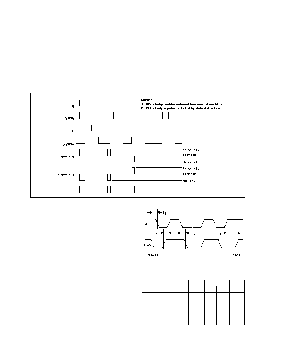
PHASE COMPARATOR
The phase comparator produces current pulses of
duration equal to the difference in phase between the
comparison frequency (fc=Rl/R), and f
VN
, the divided-down
VCO frequency (Fl/N).
When status bit 4 is set high the positive polarity mode of
the output PD is selected. When fc leads f
VN
the PD output
goes high; when f
VN
ieads fc it goes low. Similarly, selecting
the negative polarity mode of PD by programming bit 4 of the
status register low causes PD to have the inverse polarity. The
loop filter integrates the current pulses to produce a voltage
drive to the VCO.
No pulses are produced when locked. The lock detect
output, LD, produces a logic `0' pulse equal to the phase
difference between f
C
and f
VN
.
When the phase difference between fc and f
VN
is too small
to be resolved by the phase detector then no current pulses
are produced. In this region the loop does not reduce the
close-in noise on the VCO output. This can be overcome
using a very high value resistor to leak a few nanoAmps of
current from the filter and keep the loop on the edge of the
region.
Fig. 5 Phase comparator phase diagram
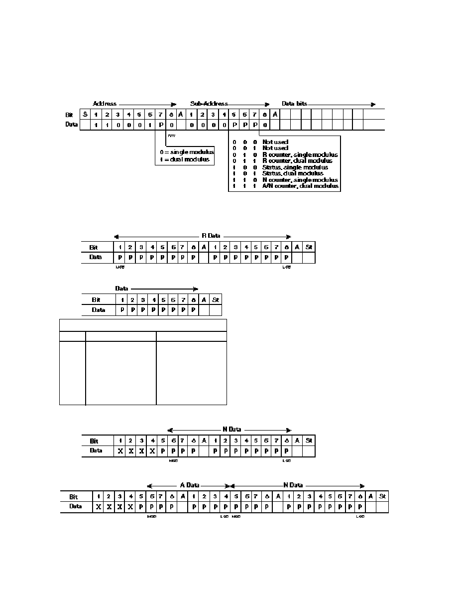
PROGRAMMING
Transmission Protocol
I
2
C programming messages consist of an address byte
followed by a sub-address byte followed by 1, 2 or 3 bytes of
data. Bit 7 of the address byte must match the setting of the
S/D pin for the address to be recognised. This allows for
separate addressing of two NJ88C33 synthesisers on the
same bus. The sub-address should be set to select the correct
registers to be programmed and should be followed by the
appropriate number of data bytes. Registers are not
programmed until the complete message protocol has been
checked.
Each message should commence with a START condition
and end with a STOP condition unless followed immediately
by another transfer, when the STOP condition may be omitted.
Data is transferred from the shift register to the latches on
a STOP condition or by a second START condition.
A START condition is indicated by a falling edge on the
Serial Data line, SDA, when the Serial Clock line. SCL, is high.
A rising edge on SDA when SCL is high indicates a STOP
condition as shown in Fig.6.
Data on SDA is clocked into the NJ88C33 on the rising
edge of SCL. The NJ88C33 acknowledges each byte
transferred to it by pulling the SDA line low for one cycle of SCL
after the last bit has been received.
Serial clock frequency
SCL hold after START
Data set-up time
Data hold after SCL low
SCL set-up before STOP
Symbol
Parameter
f
SCL
t
1
t
2
t
3
t
4
Unit
Min.
Max.
MHz
ns
ns
ns
ns
200
20
0
20
5
I2C TIMING INFORMATION
VDD = 4.5V to 5.5V, Tamb = -40�C to +85�C
Fig. 6 I
2
C timing diagram
Value
NJ88C33
7
Address and Sub-Address Formats
The correct addressing sequence for the NJ88C33 is
shown below. The START condition is followed by the
address byte, the acknowledge from the NJ88C33, the sub-
address byte, another acknowledge then the associated data.
The correct values for each address and sub-address are
listed, together with the message selection options.
S = Start
St = Stop
A = Acknowledge
P = Programmable (as shown)
x = Don't care
Data Formats
Each of the data formats should be preceded contiguously
by the addressing sequence given above.
R counter : single or dual modulus
Status : single or dual modulus
N counter : single modulus
A/N counters : dual modulus
1
2
3
4
5
6
7
8
PORT = low
Counters off
(1)
FI and RI off
(2)
PD = polarity negative
PD bias = 0.625mA
f
VD
= RI/2
Doubler off
MOD = push-pull
PORT = high
Counters on
FI and RI on
PD = polarity positive
PD bias = 2.5mA
f
VD
= RI/4
Doubler on
(3)
MOD = open drain
Status Byte
Bit
1
0
NOTES
1. In this standby mode the counters are disabled but the
voltage doubler and I
2
C interface can both function.
2. In this standby mode the FI and RI preamplifiers are
disabled, which stops the counters and the voltage doubler.
The I
2
C interface still operates.
3. The voltage doubler should only be used when V
DD
3.0V

NJ88C33
8
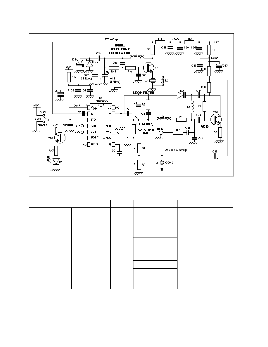
APPLICATION CIRCUITS
Single Modulus
In this mode, the NJ88C33 synthesiser can be used with
or without a fixed modulus prescaler. The R counter is
programmed with a value to produce a comparison frequency
fc. When the N counter is changed by 1 the loop is no longer
in lock and the phase detector output produces current pulses
to bring the loop back into lock. These pulses are integrated by
the loop fiiter to produce the VCO voltage drive. When the
VCO loop is locked, Fl/N=f
C
i.e., the VCO frequency is N x f
C
.
Using a prescaler with a division ratio P, the smallest VCO
output frequency step is Pf
C
and the VCO frequency is PNf
C
.
If a low pass filter is connected to the lock detect output as
shown and sampled by the microprocessor, the proximity of
the synthesiser loop to lock can be evaluated.
The A counter is not used in this mode.
Fig. 7 Single modulus application
Fig. 8 Dual modulus application
Dual Modulus
This mode allows much higher frequencies to be used in
conjunction with a prescaler but maintains the step size, fc. In
this mode, a dual modulus prescaler (with ratios P and P + 1)
must be used with the NJ88C33. The A counter controls the
MOD output, which is used to select the division ratio of the
prescaler.
When the A counter is non-zero, the MOD output is low and
goes high when the A counter has counted down to zero.
MOD remains high until the N counter reaches zero, when
both counters are re-loaded. Thus, the prescaler divides by P
for N-A cycles and by P + 1 for A cycles of Fl. The VCO
frequency is given by PNf
C
+ Af
C
.
Note that programming A = 0 produces a count of 128 cycles.

NJ88C33
9
VCO Driving Without Voltage Doubler
To switch off the voltage doubler, bit 7 of the status register
is programmed low. This will reduce current consumption and
minimise noise. The voltage doubler output C should be
connected to GND1 as connection to GND2 would induce
noise in the VCO loop.
VCO Driving With Voltage Doubler
The voltage doubler is switched on by setting bit 7 of the
status register high. It is recommended that a reservoir
capacitor of at least 1�F be connected from C to GND1.
The voltage doubler is designed to boost VCO drive in low
voltage applications.
Fig. 9 Driving a VCO without voltage doubler
Fig. 10 Driving a VCO using the voltage doubler
Further Applications Information
A stand-alone programmer card and an evaluation board
are available for evaluating the NJ88C33. The programmer
card allows two sets of variables to be programmed into both
the divider and status registers during alternate programming
cycles, at either the standard I
2
C bus rate of 100kHz or at
2MHz.
Initialisation is with either a manual push-button or by an
external logic level pulse; a synchronisation output is provided
to allow a quick assessment of `step' and `settle' responses to
be made.
The NJ88C33 evaluation board (Fig. 11 ) dernonstrates
the preferred layout technique - providing a reference
oscillator, a 60 to 80MHz VCO and a simple loop filter to
complete a minimal frequency synthesiser loop. The two units
allow analysis of different loop variables as well as the
selection of comparison frequencies for fast frequency-
hopping loops.
Application Note: AN94,
`Using the NJ88C33 PLL
Synthesiser' explains the design equations and
demonstrates the use of the device, and is available from your
local Mitel Semiconductor customer service centre.
NJ88C33
10
C0
1nF 10%
C1
100nF 10%
C2
1�F Tant.
C4
10nF 10%
C5
22�F/35V Elect.
C6
10nF 10%
C7
1nF 10%
C8
1nF 10%
C9
1nF 10%
C11 150pF 5% NPO
C12 1nF 10%
C13 1nF 10%
C14 2p7 � 0.5pF NPO
C15 10nF 10%
C16 10nF 10%
IC1
NJ88C33
X1
10.00MHz 5ppm series
SW1
Miniature slide switch
CON1
SMC socket
CON2
SMC socket
PCB
C33ISS2
C17 22�F/35V Elect.
C19 10nF 10%
C20 22�F/35V Elect.
C21 10nF 10%
C22 10nF 10%
C23 22pF 5% NPO
C24 22�F/35V Elect.
C27 22pF 5% NPO
VC1 3p5-22p
L1
15�H 10%
L2
220�H 10%
L3
180nH 20%
L4
470�H 10%
Capacitors
Miscellaneous
Resistors
D1
1N6263 Schottky
D2
1N6263 Schottky
D3
BBY40 varicap
D4
5mm red LED
TR1 BFS17 RF NPN
TR2 BFS17 RF NPN
TR3 2N3904 Switching
R1
270
R2
470
R3
330
R4
100
R5
100
R6
1k
R7
120
R8
27k
R9
Link
R10 1k
R11 10
R12 10
R13 10
R14 22k
R15 2.7k
R16 330R
R17 100
R18 33M
Inductors
Diodes
Transistors
COMPONENT LIST FOR FIG. 11
NOTES
1. With the exception of electrolytics, all capacitors are surface mount types.
2. All resistors are 0.25W, �2%.
3. C0, C1, C2, C11, C12, C13 and C14 must be low leakage types.
4. R18 may be required to optimise VCO close in noise performance.
Fig. 11 Typical applications circuit
* Insert C15, delete R4 and R5 if CON2 is to be used to monitor the VCO. Delete C15 insert R4 and R5 if CON is to provide
an external source, otherwise short C15 and delete R4, R5 and CON2.

M Mitel (design) and ST-BUS are registered trademarks of MITEL Corporation
Mitel Semiconductor is an ISO 9001 Registered Company
Copyright 1999 MITEL Corporation
All Rights Reserved
Printed in CANADA
TECHNICAL DOCUMENTATION - NOT FOR RESALE
World Headquarters - Canada
Tel: +1 (613) 592 2122
Fax: +1 (613) 592 6909
North America
Asia/Pacific
Europe, Middle East,
Tel: +1 (770) 486 0194
Tel: +65 333 6193
and Africa (EMEA)
Fax: +1 (770) 631 8213
Fax: +65 333 6192
Tel: +44 (0) 1793 518528
Fax: +44 (0) 1793 518581
http://www.mitelsemi.com
Information relating to products and services furnished herein by Mitel Corporation or its subsidiaries (collectively "Mitel") is believed to be reliable. However, Mitel assumes no
liability for errors that may appear in this publication, or for liability otherwise arising from the application or use of any such information, product or service or for any infringement of
patents or other intellectual property rights owned by third parties which may result from such application or use. Neither the supply of such information or purchase of product or
service conveys any license, either express or implied, under patents or other intellectual property rights owned by Mitel or licensed from third parties by Mitel, whatsoever.
Purchasers of products are also hereby notified that the use of product in certain ways or in combination with Mitel, or non-Mitel furnished goods or services may infringe patents or
other intellectual property rights owned by Mitel.
This publication is issued to provide information only and (unless agreed by Mitel in writing) may not be used, applied or reproduced for any purpose nor form part of any order or
contract nor to be regarded as a representation relating to the products or services concerned. The products, their specifications, services and other information appearing in this
publication are subject to change by Mitel without notice. No warranty or guarantee express or implied is made regarding the capability, performance or suitability of any product or
service. Information concerning possible methods of use is provided as a guide only and does not constitute any guarantee that such methods of use will be satisfactory in a specific
piece of equipment. It is the user's responsibility to fully determine the performance and suitability of any equipment using such information and to ensure that any publication or
data used is up to date and has not been superseded. Manufacturing does not necessarily include testing of all functions or parameters. These products are not suitable for use in
any medical products whose failure to perform may result in significant injury or death to the user. All products and materials are sold and services provided subject to Mitel's
conditions of sale which are available on request.