 | ÐлекÑÑоннÑй компоненÑ: M30802MC | СкаÑаÑÑ:  PDF PDF  ZIP ZIP |
Äîêóìåíòàöèÿ è îïèñàíèÿ www.docs.chipfind.ru

Under
development
Preliminary Specifications REV.B
Specifications in this manual are tentative and subject to change.
Mitsubishi microcomputers
M16C/80 (144-pin version) group
SINGLE-CHIP 16-BIT CMOS MICROCOMPUTER
Description
1
------Table of Contents------
Description
The M16C/80 (144-pin version) group of single-chip microcomputers are built using the high-performance
silicon gate CMOS process using a M16C/60 Series CPU core and are packaged in a 144-pin plastic
molded QFP. These single-chip microcomputers operate using sophisticated instructions featuring a high
level of instruction efficiency. With 16M bytes of address space, they are capable of executing instructions
at high speed. They also feature a built-in multiplier and DMAC, making them ideal for controlling office,
communications, industrial equipment, and other high-speed processing applications.
The M16C/80 (144-pin version) group includes a wide range of products with different internal memory
types and sizes and various package types.
Features
· Memory capacity .................................. ROM (See ROM expansion figure.)
RAM 10 to 24 Kbytes
· Shortest instruction execution time ...... 50ns (f(X
IN
)=20MHz)
· Supply voltage ..................................... 4.2 to 5.5V (f(X
IN
)=20MHz) Mask ROM and flash memory version
2.7 to 5.5V (f(X
IN
)=10MHz) Mask ROM and flash memory version
· Low power consumption ...................... 45mA (M30802MC-XXXGP)
· Interrupts .............................................. 29 internal and 8 external interrupt sources, 5 software
interrupt sources; 7 levels (including key input interrupt)
· Multifunction 16-bit timer ...................... 5 output timers + 6 input timers
· Serial I/O .............................................. 5 channels for UART or clock synchronous
· DMAC .................................................. 4 channels (trigger: 31 sources)
· DRAMC ................................................ Used for EDO, FP, CAS before RAS refresh, self-refresh
· A-D converter ....................................... 10 bits X 8 channels (Expandable up to 10 channels)
· D-A converter ....................................... 8 bits X 2 channels
· CRC calculation circuit ......................... 1 circuit
· X-Y converter ....................................... 1 circuit
· Watchdog timer .................................... 1 line
· Programmable I/O ............................... 123 lines
· Input port ..............................................
_______
1 line (P8
5
shared with NMI pin)
· Memory expansion .............................. Available (16M bytes)
· Chip select output ................................ 4 lines
· Clock generating circuit ....................... 2 built-in clock generation circuits
(built-in feedback resistance, and external ceramic or quartz oscillator)
Applications
Audio, cameras, office equipment, communications equipment, portable equipment, etc.
CPU .............................................................. 11
Reset ............................................................. 16
Processor Mode ............................................ 24
Clock Generating Circuit ............................... 40
Protection ...................................................... 52
Outline of Interrupt ........................................ 53
Watchdog Timer ............................................ 75
DMAC ........................................................... 77
Timer ............................................................. 88
Serial I/O ..................................................... 120
Specifications written in this
manual are believed to be ac-
curate, but are not guaranteed
to be entirely free of error.
Specifications in this manual
may be changed for functional
or performance improvements.
Please make sure your manual
is the latest edition.
A-D Converter ............................................. 162
D-A Converter ............................................. 172
CRC Calculation Circuit .............................. 174
X-Y Converter ............................................. 176
DRAM Controller ......................................... 179
Programmable I/O Ports ............................. 186
Usage Precaution ....................................... 203
Electric characteristics ................................ 210
Flash memory version ................................. 257
Under
development
Preliminary Specifications REV.B
Specifications in this manual are tentative and subject to change.
Mitsubishi microcomputers
M16C/80 (144-pin version) group
SINGLE-CHIP 16-BIT CMOS MICROCOMPUTER
Description
2
109
110
111
112
113
114
115
116
117
118
119
120
121
122
123
124
125
126
127
128
129
130
131
132
133
134
135
136
137
138
139
140
141
142
143
144
P9
6
/ANEX
1
/T
X
D
4
/SDA
4
/SRxD
4
P9
5
/ANEX
0
/CLK
4
P9
2
/TB
2IN
/T
X
D
3
/SDA
3
/SRxD
3
P9
1
/TB
1IN
/R
X
D
3
/SCL
3
/STxD
3
P9
0
/TB
0IN
/CLK3
P14
6
P14
5
P14
4
P14
3
P14
1
P14
2
P14
0
BYTE
CNV
SS
P8
7
/X
CIN
P8
6
/X
COUT
X
OUT
V
SS
X
IN
V
CC
P8
0
/TA
4OUT
/U
P7
7
/TA
3IN
P7
6
/TA
3OUT
P7
4
/TA
2OUT
/W
P7
2
/CLK
2
/TA
1OUT
/V
(Note)
P7
1
/R
X
D
2
/SCL
2
/TA
0IN
/TB
5IN
(Note)
P9
4
/DA
1
/TB
4IN
/CTS
4
/RTS
4
/SS
4
P9
3
/DA
0
/TB
3IN
/CTS
3
/RTS
3
/SS
3
RESET
P8
5
/NMI
P8
4
/INT
2
P8
3
/INT
1
P8
2
/INT
0
P8
1
/TA
4IN
/U
P7
5
/TA
2IN
/W
P7
3
/CTS
2
/RTS
2
/TA
1IN
/V
37
38
39
40
41
42
43
44
45
46
47
48
49
50
51
52
53
54
55
56
57
58
59
60
61
62
63
64
65
66
67
68
69
70
71
72
P7
0
/T
X
D
2
/SDA
2
/TA
0OUT
P6
7
/T
X
D
1
V
CC
P6
6
/R
X
D
1
V
SS
P6
5
/CLK
1
P6
3
/T
X
D
0
P6
2
/R
X
D
0
P6
1
/CLK
0
P13
7
P13
6
P13
5
P13
4
P13
3
V
SS
P13
2
V
CC
P13
1
P13
0
P5
3
/BCLK/ALE/CLK
OUT
P12
7
P12
6
P12
5
P6
4
/CTS
1
/RTS
1
/CTS
0
/CLKS
1
P6
0
/CTS
0
/RTS
0
P5
6
/ALE/RAS
P5
5
/HOLD
P5
4
/HLDA/ALE
P5
2
/RD/DW
P5
1
/WRH/BHE/CASH
P5
0
/WRL/WR/CASL
P4
7
/CS0/A
23
P4
6
/CS1/A
22
P4
5
/CS2/A
21
P4
4
/CS3/A
20
(MA12)
P4
3
/A
19
(MA11)
V
CC
P4
2
/A
18
(MA10)
V
SS
P4
1
/A
17
(MA9)
P4
0
/A
16
(MA8)
P3
7
/A
15
(MA7)(/D
15
)
P3
6
/A
14
(MA6)(/D
14
)
P3
5
/A
13
(MA5)(/D
13
)
P3
4
/A
12
(MA4)(/D
12
)
P3
3
/A
11
(MA3)(/D
11
)
P3
2
/A
10
(MA2)(/D
10
)
P3
1
/A
9
(MA1)(/D
9
)
P12
4
P12
3
P12
2
P12
1
P12
0
V
CC
P3
0
/A
8
(MA0)(/D
8
)
P2
7
/A
7
(/D
7
)
P2
6
/A
6
(/D
6
)
P2
5
/A
5
(/D
5
)
P2
4
/A
4
(/D
4
)
P2
3
/A
3
(/D
3
)
P2
2
/A
2
(/D
2
)
P2
1
/A
1
(/D
1
)
P2
0
/A
0
(/D
0
)
V
SS
P1
4
/D
12
P1
3
/D
11
P1
2
/D
10
P1
1
/D
9
P1
5
/D
13
/INT3
P1
6
/D
14
/INT4
P1
7
/D
15
/INT5
P1
0
/D
8
P0
7
/D
7
P0
6
/D
6
P0
5
/D
5
P0
4
/D
4
P11
4
P11
3
P11
2
P11
1
P11
0
P0
3
/D
3
P0
2
/D
2
P0
1
/D
1
P0
0
/D
0
P15
7
P15
6
P15
5
P15
4
P15
3
P15
2
P15
1
V
SS
P15
0
V
CC
P10
3
/AN
3
P10
2
/AN
2
P10
1
/AN
1
AV
SS
P10
0
/AN
0
V
REF
AV
CC
P10
7
/AN
7
/KI3
P10
6
/AN
6
/KI2
P10
5
/AN
5
/KI1
P10
4
/AN
4
/KI0
P9
7
/AD
TRG
/R
X
D
4
/SCL
4
/STxD
4
73
74
75
76
77
79
80
81
82
83
84
85
86
87
88
89
90
91
92
93
94
95
96
97
98
99
100
101
102
103
104
105
106
107
108
78
P5
7
/RDY
1
2
3
4
7
6
8
9
10 11 12 13 14 15 16 17 18 19 20 21 22 23 24 25 26 27 28 29 30
5
31 32 33 34 35 36
Note: This port is N-channel open drain output.
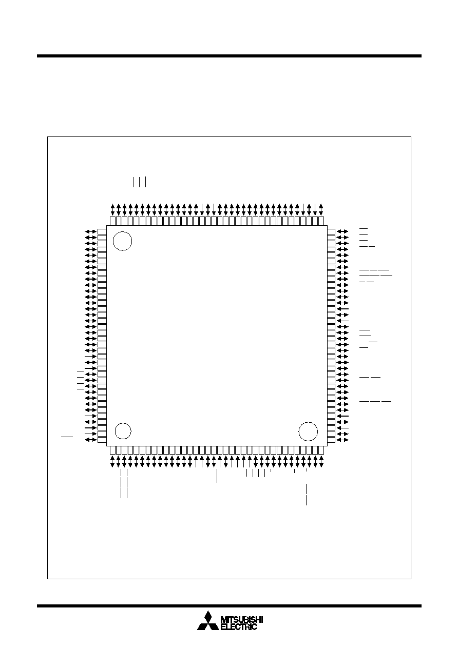
M30802-XXXGP
Pin Configuration
Figure 1.1.1 show the pin configurations (top view).
PIN CONFIGURATION (top view)
Package: 144P6Q-A
Figure 1.1.1. Pin configuration (top view)
Under
development
Preliminary Specifications REV.B
Specifications in this manual are tentative and subject to change.
Mitsubishi microcomputers
M16C/80 (144-pin version) group
SINGLE-CHIP 16-BIT CMOS MICROCOMPUTER
Description
3
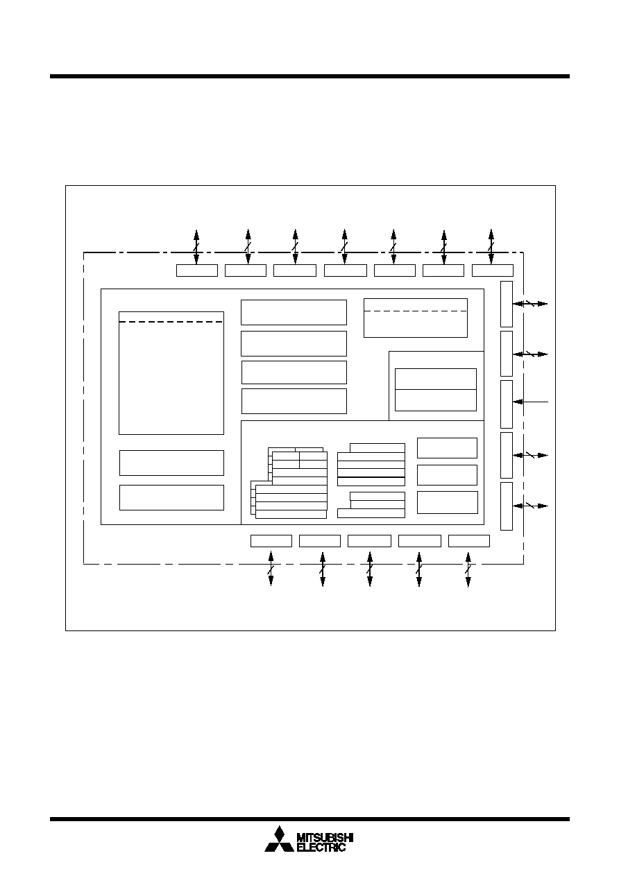
Block Diagram
Figure 1.1.2 is a block diagram of the M16C/80 (144-pin version) group.
Block diagram of the M30802MC-XXXGP
Figure 1.1.2. Block diagram of M30802MC-XXXGP
R0L
R0H
R1H
R1L
R2
I/O ports
8
8
8
8
8
8
8
8
7
8
8
Internal peripheral functions
Timer
Timer TA0 (16 bits)
Timer TA1 (16 bits)
Timer TA2 (16 bits)
Timer TA3 (16 bits)
Timer TA4 (16 bits)
Timer TB0 (16 bits)
Timer TB1 (16 bits)
Timer TB2 (16 bits)
Timer TB3 (16 bits)
Timer TB4 (16 bits)
Timer TB5 (16 bits)
Watchdog timer
(15 bits)
D-A converter
(8 bits X 2 channels)
A-D converter
(10 bits X 8 channels
Expandable up to 10 channels)
UART /clock synchronous SI/O
(8 bits X 5 channels)
X-Y converter
(16 bits X 16 bits)
CRC arithmetic circuit (CCITT)
(Polynomial : X +X +X +1)
System clock generator
X
IN
- X
OUT
X
CIN
- X
COUT
Memory
DRAM
controller
M16C/80 series 16-bit CPU core
Registers
R0H
R0L
R1H
R1L
R2
R3
A0
A1
FB
SB
DRAM
controller
Multiplier
Port P0
Port P1
Port P2
Port P3
Port P4
Port P5
Port P6
Port P7
Port P8
Port P8
5
Port P9
Port P10
FLG
INTB
ISP
USP
PC
SVF
SVP
VCT
12
16
5
ROM
(Note 1)
RAM
(Note 2)
Note 1: ROM size depends on MCU type.
Note 2: RAM size depends on MCU type.
Port P15
Port P14
Port P13
Port P12
Port P11
8
7
8
8
5
Under
development
Preliminary Specifications REV.B
Specifications in this manual are tentative and subject to change.
Mitsubishi microcomputers
M16C/80 (144-pin version) group
SINGLE-CHIP 16-BIT CMOS MICROCOMPUTER
Description
4
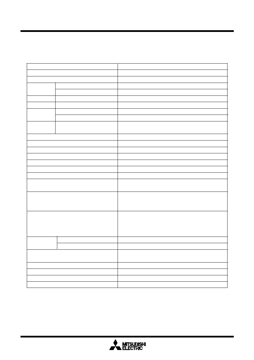
Item
Performance
Number of basic instructions
106 instructions
Shortest instruction execution time
50ns(f(X
IN
)=20MHz)
Memory
See ROM expansion figure.
capacity
10 to 24 K bytes
I/O port
8 bits x 13, 7 bits x 2, 5 bits x 1
Input port
1 bit x 1
Multifunction
16 bits x 5
timer
16 bits x 6
Serial I/O
(UART or clock synchronous) x 5
A-D converter
10 bits x (8 + 2) channels
D-A converter
8 bits x 2
DMAC
4 channels
DRAM controller
CAS before RAS refresh, self-refresh, EDO, FP
CRC calculation circuit
CRC-CCITT
X-Y converter
16 bits X 16 bits
Watchdog timer
15 bits x 1 (with prescaler)
Interrupt
29 internal and 8 external sources, 5 software sources, 7
levels
Clock generating circuit
2 built-in clock generation circuits
(built-in feedback resistance, and external ceramic or
quartz oscillator)
Supply voltage
4.2 to 5.5V (f(X
IN
)=20MHz) Mask ROM and flash
memory version
2.7 to 5.5V (f(X
IN
)=10MHz) Mask ROM and flash
memory version
Power consumption
45mA (f(X
IN
) = 20MHz without software wait,Vcc=5V)
Mask ROM 128 Kbytes version
I/O
5V
characteristics
5mA
Memory expansion
Available (up to 16M bytes)
Operating ambient temperature
40 to 85
o
C
Device configuration
CMOS high performance silicon gate
Package
144-pin plastic mold QFP
Table 1.1.1. Performance outline of M16C/80 (144-pin version) group
Performance Outline
Table 1.1.1 is a performance outline of M16C/80 (144-pin version) group.
ROM
RAM
P0 to P15 (except P8
5
)
P8
5
TA0, TA1, TA2, TA3,TA4
TB0, TB1, TB2, TB3, TB4, TB5
UART0, UART1, UART2,
UART3, UART4
I/O withstand voltage
Output current
Under
development
Preliminary Specifications REV.B
Specifications in this manual are tentative and subject to change.
Mitsubishi microcomputers
M16C/80 (144-pin version) group
SINGLE-CHIP 16-BIT CMOS MICROCOMPUTER
Description
5
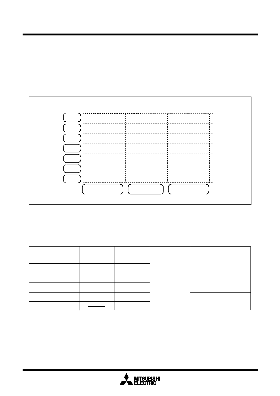
Mitsubishi plans to release the following products in the M16C/80 (144-pin version) group:
(1) Support for mask ROM version, external ROM version and flash memory version
(2) ROM capacity
(3) Package
144P6Q
: Plastic molded QFP (mask ROM version and flash memory version)
The M16C/80 (144-pin version) group products currently supported are listed in Table 1.1.2.
RAM capacity
ROM capacity
Package type
Remarks
Type No
10K bytes
Mask ROM version
As of June, 2000
M30802MC-XXXGP
128K bytes
M30802FCGP
**
**
:Under development
Flash memory version
144P6Q-A
M30805FGGP
**
20K bytes
256K bytes
M30802SGP
10K bytes
External ROM version
20K bytes
M30805MG-XXXGP
256K bytes
10K bytes
128K bytes
M30805SGP
24K bytes
Table 1.1.2. M16C/80 (144-pin version) group
Figure 1.1.3. ROM expansion
ROM Size
(Byte)
External
ROM
128K
96K
64K
32K
Mask ROM version
Flash memory
version
External ROM version
80K
256K
M30802MC-XXXGP
M30802FCGP
M30805FGGP
M30802SGP
M30805MG-XXXGP
M30805SGP
Document Outline