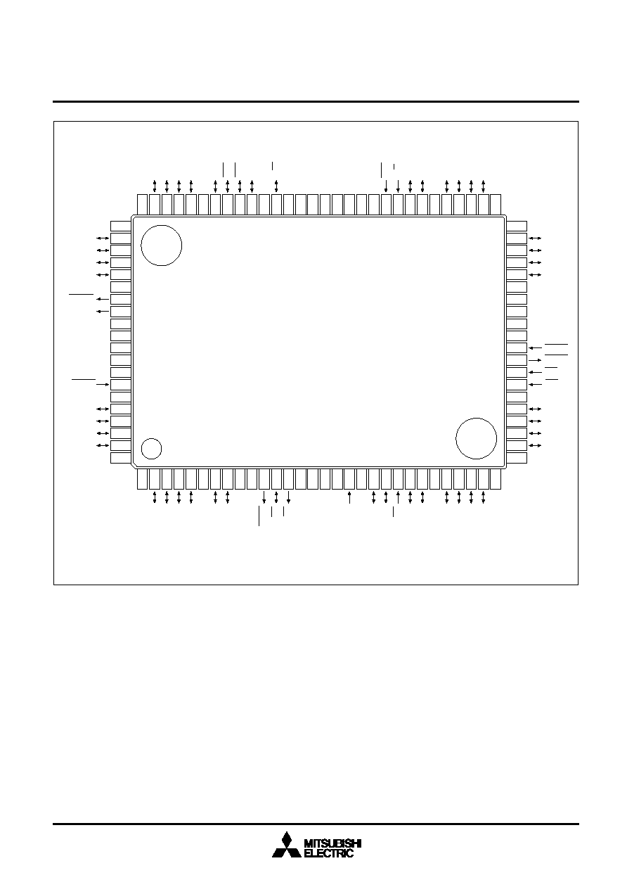
SINGLE-CHIP 32-BIT CMOS MICROCOMPUTER
FEATURES
∑
CPU .......................................................... M32R family CPU core
∑
Pipeline .............................................................................. 5 steps
∑
Basic bus cycle ................................. 15 ns (at internal 66.6 MHz)
∑
Logical address space ............................................ 4G-byte linear
∑
External bus ........................................................ data bus: 16 bits
address bus: 24 bits
∑
Internal DRAM ................................................. 8M bits (1M bytes)
∑
Cache .......................................................... 4K bytes (direct map)
∑
Register configuration ...... general-purpose registers: 32 bits x 16
control registers: 32 bits x 5
∑
Instruction set ....................... 83 instructions/6 addressing modes
∑
Instruction format .................................................... 16 bits/32 bits
∑
Multiply-accumulate operation unit (DSP function instruction)
∑
Internal memory controller
∑
Programmable I/O ports
∑
Power management function .................................. standby mode
/CPU sleep mode
∑
PLL clock generating circuit ................. four-time clock PLL circuit
∑
Operation mode .............................................. master/slave mode
∑
Interrupt input ............................................................
___
___
INT and SBI
∑
Power source .......................................................... 3.3 V (±10 %)
APPLICATIONS
Portable equipment, Still camera, Navigation system,
Digital instrument, Printer, Scanner, FA equipment
DESCRIPTION
The M32000D3FP is a new generation microcomputer with a 32-bit
CPU and built-in high capacity DRAM. Using this device it is possible
to implement the complex applications of the multimedia age with
high performance and low power consumption.
The M32000D3FP contains 1M bytes of DRAM and 4K bytes of cache
memory. The CPU is implemented with a RISC architecture and has
a high performance figure of 52.4 MIPS (at an internal clock rate of
66.6 MHz ). Memory for main storage is provided internally to the
device eliminating external memory and associated control circuits
thus reducing overall system noise and power consumption.
The CPU, internal DRAM and cache memory are connected by a
128-bit, 15 ns/cycle internal bus which virtually eliminates transfer
bottlenecks in between the CPU and the memory. The M32000D3FP
internally multiplies the frequency of the input clock signals by four.
For an internal operating frequency of 66.6 MHz the input clock fre-
quency is 16.65MHz.
A 16-bit data and 24-bit address bus are the M32000D3FP's exter-
nal bus and the interface to external peripheral controllers. When the
hold state is set, the internal DRAM can be accessed from an exter-
nal device.
A 3-chip basic system configuration using the M32000D3FP is the
device itself plus an ASIC as a peripheral controller and a program
ROM. Execution starts from the reset vector entry on the external
ROM after power on, a program requiring high speed execution is
then transferred to internal DRAM and this is then executed. The
M32000D3FP also has a slave mode additional to its master mode.
When set to slave mode the M32000D3FP can be used as a
coprocessor. In this mode it does not access its external bus
immediatly after reset, but waits for the master to start its operation.
MITSUBISHI MICROCOMPUTERS
M32000D3FP

SINGLE-CHIP 32-BIT CMOS MICROCOMPUTER
MITSUBISHI MICROCOMPUTERS
M32000D3FP
4
FUNCTIONS
function block
characteristics
CPU core
∑ bus specification
basic bus cycle: 15 ns (internal operation at 66.6 MHz)
logical address space: linear 4G bytes
____
____
external address bus: 24 bits (external output pin: A8 to A30, BCH, BCL)
external data bus: 16 bits
∑ implementation: 5-stage pipeline
∑ core internal: 32 bits
∑ register configuration
general-purpose registers: 32 bits
!
16
control registers: 32 bits
!
5
∑ instruction set
16-bit/32-bit instruction format
83 instructions/6 addressing modes
∑ multiply-accumulate operation built in
internal DRAM
∑ 8M bits (1M bytes)
cache memory
∑ 4K bytes (internal instruction/data cache mode, instruction cache mode, cache-off mode)
memory controller
∑ cache control
∑ internal DRAM control, refresh control
∑ power management function (standby mode, CPU sleep mode selection control)
programmable I/O port
∑ two programmable I/O ports