 | –≠–ª–µ–∫—Ç—Ä–æ–Ω–Ω—ã–π –∫–æ–º–ø–æ–Ω–µ–Ω—Ç: M35500AFP | –°–∫–∞—á–∞—Ç—å:  PDF PDF  ZIP ZIP |
Document Outline
- DESCRIPTION/FERTURES
- FUNCTIONAL BLOCK
- PIN DESCRIPTION
- COMMAND STYLE
- SERIAL I/O PROTOCOL
- SERIAL COMMUNICATION FORMAT
- FLD DISPLAY TIMING
- BIT ALLOCATION FOR DISPLAY RAM
- RESET CIRCUIT
- CLOCK GENERATING CIRCUIT
- HANDLING OF UNUSED PINS
- ABSOLUTE MAXIMUM RATINGS
- RECOMMENDED OPERATING CONDITIONS
- ELECTRICAL CHARACTERISTICS
- A-D CONVERTER CHARACTERISTICS
- TIMING REQUIREMENTS
- SWITCHING CHARACTERISTICS
- PACKAGE OUTLINE
- REVISION HISTORY
1
MITSUBISHI <DIGITAL ASSP>
M35500AFP/BGP
FLD(VFD) CONTROLLER
DESCRIPTION/FEATURES
∑
High-breakdown-voltage output port ......................................... 26
∑ Segment output ............................................ 8 to 18
∑ Digit output ................................................... 7 to 10
(Ports P0 to P7 are also used as ordinary output ports)
∑ Output breakdown .................................. Vcc ≠ 45 V
∑ Output current .................. ≠18 mA (DIG
0
to DIG
17
),
≠7 mA (SEG
0
to SEG
7
)
∑ Pull-down resistor ........................................ build-in
∑ Dimmer switch ............................................ 4 levels
∑
A-D converter ................................................... 8-bit
!
6 channels
∑ Absolute accuracy ....................................... ±3 LSB
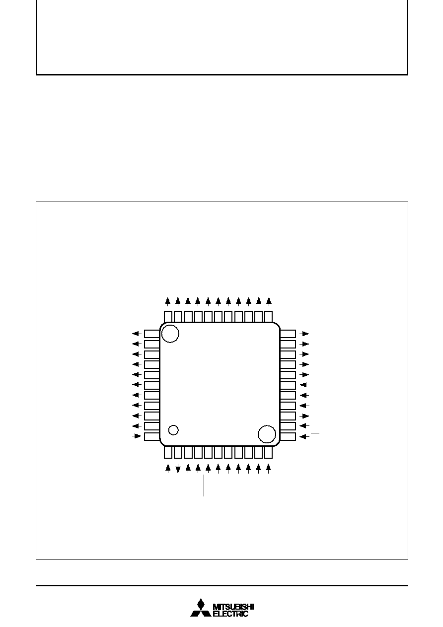
PIN CONFIGURATION (TOP VIEW)
∑
Serial I/O ..................................... 4 (CS controller, external clock)
∑ Noise filter .................................................... build-in
(in serial input pin and clock pin, 2 MHz sampling)
∑ FLD display data ............................................. input
∑ A-D conversion data ..................................... output
∑ Command ....................................................... input
∑
Package ................................................................. 44P6N/44P6X
∑
Oscillating circuit ........... RC oscillating cirucit (external capacitor)
∑ Oscillating frequency ..................................... 4 MHz
∑
Power source voltage .................................................. 4.0 to 5.5 V
Fig. 1. Pin configuration of M35500AFP/BGP
Package type: 44P6N-A/44P6X
1
2
2
M
3
5
5
0
0
A
F
P
M
3
5
5
0
0
B
G
P
3
3
3
2
3
0
3
1
2
9
2
6
2
8
2
7
2
5
2
4
2
3
D
I
G
1
5
/
S
E
G
1
0
D
I
G
1
4
/
S
E
G
1
1
D
I
G
1
3
/
S
E
G
1
2
D
I
G
1
2
/
S
E
G
1
3
D
I
G
1
1
/
S
E
G
1
4
D
I
G
1
0
/
S
E
G
1
5
D
I
G
9
/
S
E
G
1
6
D
I
G
8
/
S
E
G
1
7
D
I
G
6
/
P
6
D
I
G
7
/
P
7
D
I
G
5
/
P
5
D
I
G
1
6
/
S
E
G
9
D
I
G
1
7
/
S
E
G
8
S
E
G
7
S
E
G
6
S
E
G
5
S
E
G
4
S
E
G
3
S
E
G
2
S
E
G
1
S
E
G
0
V
D
D
3
4
3
5
3
6
3
7
3
8
3
9
4
0
4
1
4
2
4
3
4
4
V
D
D
X
O
U
T
V
S
S
X
I
N
R
E
S
E
T
A
N
5
A
N
4
A
N
3
A
N
2
A
N
1
A
N
0
D
I
G
4
/
P
4
D
I
G
3
/
P
3
D
I
G
2
/
P
2
D
I
G
1
/
P
1
D
I
G
0
/
P
0
V
E
E
V
E
E
S
C
L
K
S
O
U
T
S
I
N
C
S
2
3
4
5
6
7
8
9
1
0
1
1
2
1
2
0
1
9
1
8
1
7
1
6
1
5
1
4
1
3
1
2
2
MITSUBISHI <DIGITAL ASSP>
M35500AFP/BGP
FLD(VFD) CONTROLLER
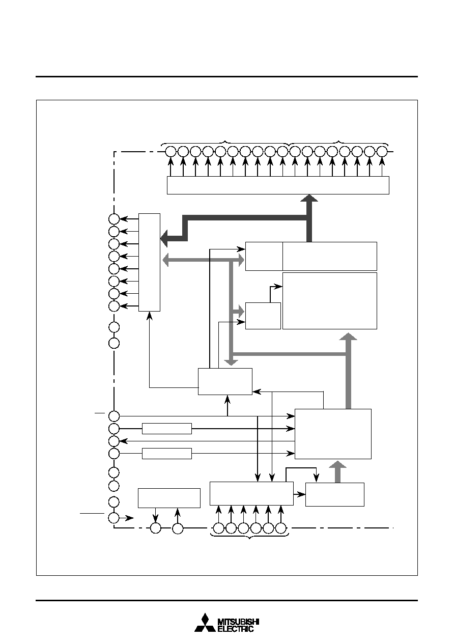
FUNCTIONAL BLOCK
Fig. 2. Functional block diagram
FUNCTIONAL BLOCK DIAGRAM (Package: 44P6N-A)
Display RAM
Display control circuit
A-D
Serial I/O
Mode
register
Command
analytic circuit
Transfer
counter
Byte end
Memory
address
Selector/A-D
control circuit
Trigger
AN
5
≠ AN
0
DIG
8
/SEG
17
≠ DIG
17
/SEG
8
SEG
7
≠ SEG
0
6
7
8
9
10
11
43
42
41
40
39
38
37
36
35
34
33
32
31
30
29
28
27
26
25
24
23
22
21
20
19
18
12
13
14
15
17
V
EE
Clock generating
circuit
2
4
X
OUT
1
3
5
Noise filter
16
V
EE
V
DD 44
DIG
7
/P7
DIG
6
/P6
DIG
5
/P5
DIG
4
/P4
DIG
3
/P3
DIG
2
/P2
DIG
1
/P1
DIG
0
/P0
X
IN
V
DD
V
SS
RESET
CS
S
IN
S
OUT
S
CLK
Noise filter
3
MITSUBISHI <DIGITAL ASSP>
M35500AFP/BGP
FLD(VFD) CONTROLLER
Table. 1. Pin description
Function
∑ Apply voltage of 5 V to V
CC
, and 0 V to V
SS
.
∑ Applies voltage supplied to pull-down resistors.
∑ RC oscillator pins for system clock.
∑ Reset input pin for active "L".
∑ Internal pull-up resistors connected between the RESET and V
CC
pins.
∑ Serial transfer is possible by inputting "L" signal.
∑ Clock for serial transfer is input.
∑ Read a clock twice with 2 MHz sampling clock and judge if it is a noise or not.
∑ Serial data is output.
∑ During reset it is in high-impedance state.
∑ Serial data is input.
∑ Read a clock twice with 2 MHz sampling clock and judge if it is a noise or not.
∑ Pin for ordinary output or digit output.
∑ At reset this port is set to V
EE
level through a pull-down resistor.
∑ Pin for digit output or segment output.
∑ At reset this port is set to V
EE
level through a pull-down resistor.
∑ Pin for segment output.
∑ At reset this port is set to V
EE
level through a pull-down resistor.
Output
Output
N-channel
open-drain
P-channel
open-drain
P-channel
open-drain
P-channel
open-drain
Pin
V
CC
, V
SS
V
EE
X
IN
X
OUT
______
RESET
____
CS
S
CLK
S
OUT
S
IN
DIG
0
/P0 ≠
DIG
7
/P7
DIG
8
/SEG
17
≠
DIG
17
/SEG
8
SEG
0
≠ SEG
7
Name
Power source
Pull-down
power source
Clock input
Clock output
______
RESET input
Chip select
Serial clock
Serial output
Serial input
Digit/Port
Digit/Segment
Segment
Input
Input
CMOS input
CMOS input
CMOS input
Noise filter
CMOS input
Noise filter
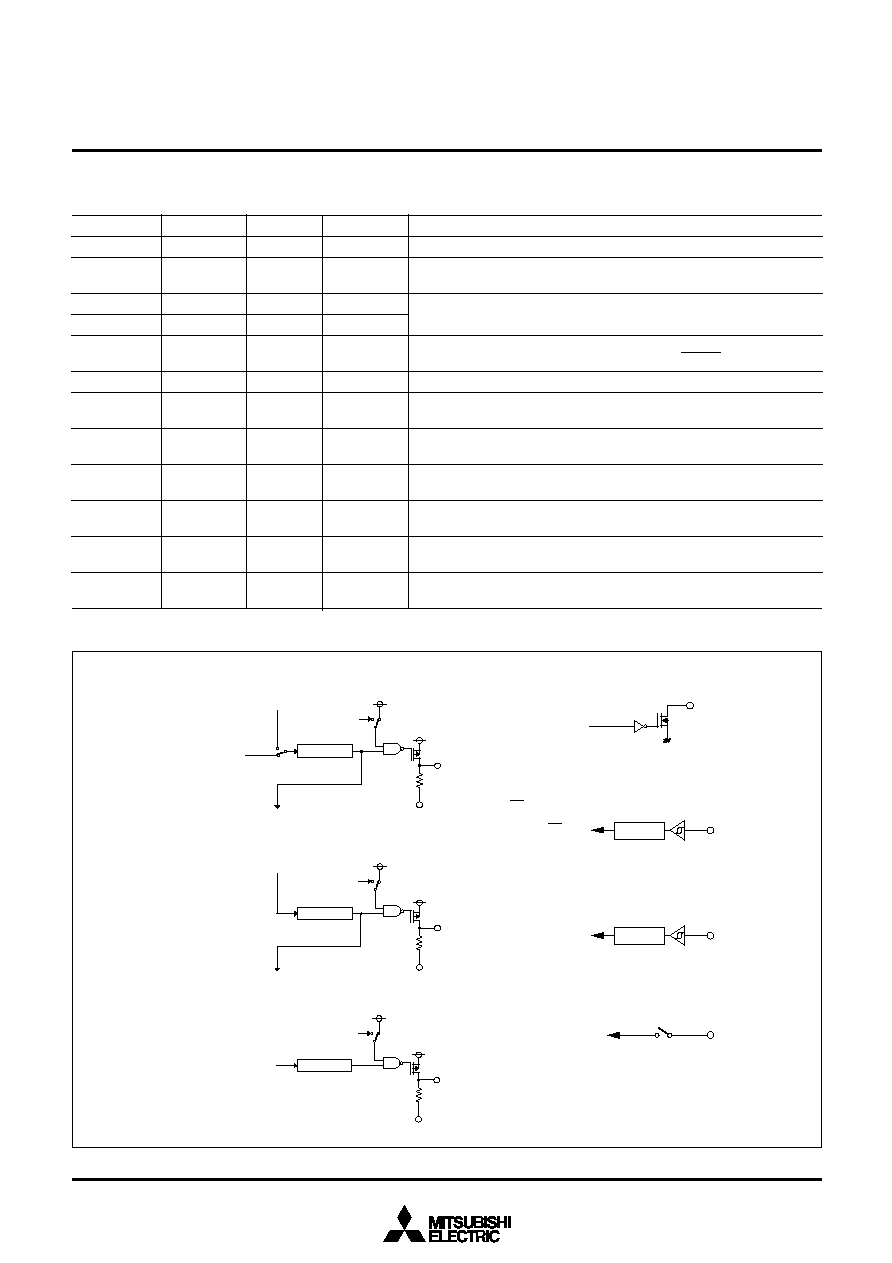
PORT BLOCK
Fig. 3. Port block diagram
PIN DESCRIPTION
(2) Digit pin
latch
V
EE
Dimmer signal
(Note)
Shift signal from high-order
Shift signal to low-order
(3) Segment pin
latch
V
EE
Dimmer signal
(Note)
Segment data
(6) S
IN
, S
CLK
pin
Serial input
Serial clock input
Noise filter
(1) Digit/Port pin
Digit/Segment pin
Data bus
Segment data
latch
V
EE
Dimmer signal
(Note)
Shift signal from high-order
Shift signal to low-order
V
High-breakdown-voltage P-channel transistor
Note: Dimmer signal is for setting the Toff time.
S
OUT
signal
(4) S
OUT
pin
(5) CS pin
CS input
A-D conversion input
(7) A-D input
Noise filter
V
V
V

4
MITSUBISHI <DIGITAL ASSP>
M35500AFP/BGP
FLD(VFD) CONTROLLER
COMMAND STYLE
Fig. 4. Command style
Port data setting
(Command 3)
1
0
0
P3 ≠ P0/P7 ≠ P4 output data
Display data setting
(Command 0)
1
1
1
Number of segment setting
0 0 : 16 or less
0 1 : 17 or more
b0
b1
b2
b3
b4
b5
b6
b7
Digit selection
(Command 2)
1
0
Digit start pin setting
0 0 0 0 : D
17
0 0 0 1 : D
16
0 0 1 0 : D
15
0 0 1 1 : D
14
0 1 0 0 : D
13
0 1 0 1 : D
12
0 1 1 0 : D
11
0 1 1 1 : D
10
1 0 0 0 : D
9
1 0 0 1 : D
8
1 0 1 0 : D
7
1
Display state setting
(Command 1)
1
1
0
Display ON or OFF setting
1 : ON
0 : OFF
Number of digit setting
0 0 : 7
0 1 : 8
1 0 : 9
1 1 : 10
Display duty setting
1 1 : 15/16
1 0 : 14/16
0 1 : 6/16
0 0 : 5/16
Port selection (Note)
0 : P3 ≠ P0
1 : P7 ≠ P4
Note: When a digit or a port has to be selected, a digit output is selected for having higher priority.
--
--
--
--

5
MITSUBISHI <DIGITAL ASSP>
M35500AFP/BGP
FLD(VFD) CONTROLLER
Byte protocol
Command protocol
Display data setting
(Command 0)
CLK
S
IN
S
OUT
Command 0
Data 1
Data 2
X
A-D
data 0
A-D
data j
CS
CLK
S
IN
S
OUT
X
b0
b1
b2
b3
b4
b5
b6
b7
b0
b1
b2
b3
b4
b5
b6
b7
Other setting except
display data setting
(Command 1 to 3)
CLK
S
IN
S
OUT
Command
X
Note: S
OUT
is in high-impedance state during CS signal is "H".
Note 1: The serial data which is transmitted after executing command 0
is recognized as a display data.
"A-D data 6 or more" data is defined as an undefined "X".
Note 2: Set the CS signal to "H" level after transferring a display data.
X
Data i
CS
CS
SERIAL I/O PROTOCOL
Fig. 5. Serial I/O protocol