
MITSUBISHI MICROCOMPUTERS
M37736EHLXXXHP
DESCRIPTION
The M37736EHLXXXHP is a single-chip microcomputer using the
7700 Family core. This single-chip microcomputer has a CPU and a
bus interface unit. The CPU is a 16-bit parallel processor that can be
an 8-bit parallel processor, and the bus interface unit enhances the
memory access efficiency to execute instructions fast. This
microcomputer also includes a 32 kHz oscillation circuit, in addition
to the PROM, RAM, multiple-function timers, serial I/O, A-D converter,
and so on.
Its strong points are the low power dissipation, the low supply voltage,
and the small package.
In the M37736MHLXXXHP, as the multiplex method of the external
bus, either of 2 types can be selected.
T h e M 3 7 7 3 6 E H L X X X H P h a s t h e s a m e f u n c t i o n a s t h e
M37736MHLXXXHP except that the built-in ROM is PROM. (Refer
to the basic function blocks description.)
FEATURES
q
Number of basic instructions .................................................. 103
q
Memory size
PROM ................................................. 124 Kbytes
RAM ................................................ 3968 bytes
q
Instruction execution time
The fastest instruction at 12 MHz frequency ...................... 333 ns
q
Single power supply ...................................................... 2.7≠5.5 V
q
Low power dissipation (At 3 V supply voltage, 12 MHz frequency)
............................................ 9 mW (Typ.)
q
Interrupts ............................................................ 19 types, 7 levels
q
Multiple-function 16-bit timer ................................................. 5 + 3
q
Serial I/O (UART or clock synchronous) ..................................... 3
q
10-bit A-D converter .............................................. 8-channel inputs
q
12-bit watchdog timer
q
Programmable input/output, output
(ports P0, P1, P2, P3, P4, P5, P6, P7, P8, P9, P10) ............... 84
q
Clock generating circuit ........................................ 2 circuits built-in
q
Small package ..................... 100-pin plastic molded fine-pitch QFP
(100P6Q-A;0.5 mm lead pitch)
APPLICATION
Control devices for general commercial equipment such as office
automation, office equipment, personal information equipment, and
others.
Control devices for general industrial equipment such as
communication equipment, and others.
PRELIMINARY
Notice: This is not a final specification.
Some parametric limits are subject to change.
Outline 100P6Q-A
50
49
48
47
46
45
44
43
42
41
40
39
38
37
36
35
34
33
32
31
30
29
28
27
26
P2
3
/A
19
/A
3
/D
3
P2
4
/A
20
/A
4
/D
4
P2
5
/A
21
/A
5
/D
5
P2
6
/A
22
/A
6
/D
6
P2
7
/A
23
/A
7
/D
7
P3
0
/R/W/WEL
P3
1
/BHE/WEH
P3
2
/ALE
P3
3
/HLDA
EVL0
EVL1
M37736EHLXXXHP
V
CC
V
SS
E/RDE
X
OUT
X
IN
RESET
BSEL
CNV
SS
BYTE
P4
0
/HOLD
P4
1
/RDY
P4
2
/
f
1
P4
3
P4
4
76
77
78
79
80
81
82
83
84
85
86
87
88
89
90
91
92
93
94
95
96
97
98
99
100
P9
1
/CLK
2
P9
0
/CTS
2
P8
7
/T
X
D
1
P8
6
/R
X
D
1
P8
5
/CLK
1
P8
4
/CTS
1
/RTS
1
P8
3
/T
X
D
0
P8
2
/R
X
D
0
/CLKS
0
P8
1
/CLK
0
P8
0
/CTS
0
/RTS
0
/CLKS
1
V
CC
AV
CC
V
REF
AV
SS
V
SS
P7
7
/AN
7
/X
CIN
P7
6
/AN
6
/X
COUT
P7
5
/AN
5
/AD
TRG
P7
4
/AN
4
P7
3
/AN
3
P7
2
/AN
2
P7
1
/AN
1
P7
0
/AN
0
P6
7
/TB2
IN
/
f
SUB
P6
6
/TB1
IN
75
74
73
72
71
70
69
68
67
66
65
64
63
62
61
60
59
58
57
56
55
54
53
52
51
1
2
3
4
5
6
7
8
9
10
11
12
13
14
15
16
17
18
19
20
21
22
23
24
25
P9
2
/R
X
D
2
P9
3
/T
X
D
2
P9
4
P9
5
P9
6
P9
7
P0
0
/A
0
/CS
0
P0
1
/A
1
/CS
1
P0
2
/A
2
/CS
2
P0
3
/A
3
/CS
3
P0
4
/A
4
/CS
4
P0
5
/A
5
/RSMP
P0
6
/A
6
/A
16
P0
7
/A
7
/A
17
P1
0
/A
8
/D
8
P1
1
/A
9
/D
9
P1
2
/A
10
/D
10
P1
3
/A
11
/D
11
P1
4
/A
12
/D
12
P1
5
/A
13
/D
13
P1
6
/A
14
/D
14
P1
7
/A
15
/D
15
P2
0
/A
16
/A
0
/D
0
P2
1
/A
17
/A
1
/D
1
P2
2
/A
18
/A
2
/D
2
P6
5
/TB0
IN
P6
4
/INT
2
P6
3
/INT
1
P6
2
/INT
0
P6
1
/TA4
IN
P6
0
/TA4
OUT
P5
7
/TA3
IN
P5
6
/TA3
OUT
P5
5
/TA2
IN
P5
4
/TA2
OUT
P5
3
/TA1
IN
P5
2
/TA1
OUT
P5
1
/TA0
IN
P5
0
/TA0
OUT
P10
7
/KI
3
P10
6
/KI
2
P10
5
/KI
1
P10
4
/KI
0
P10
3
P10
2
P10
1
P10
0
P4
7
P4
6
P4
5
PIN CONFIGURATION (TOP VIEW)
PROM VERSION OF M37736MHLXXXHP
PRELIMINARY
Notice: This is not a final specification.
Some parametric limits are subject to change.
2
PROM VERSION OF M37736MHLXXXHP
MITSUBISHI MICROCOMPUTERS
M37736EHLXXXHP
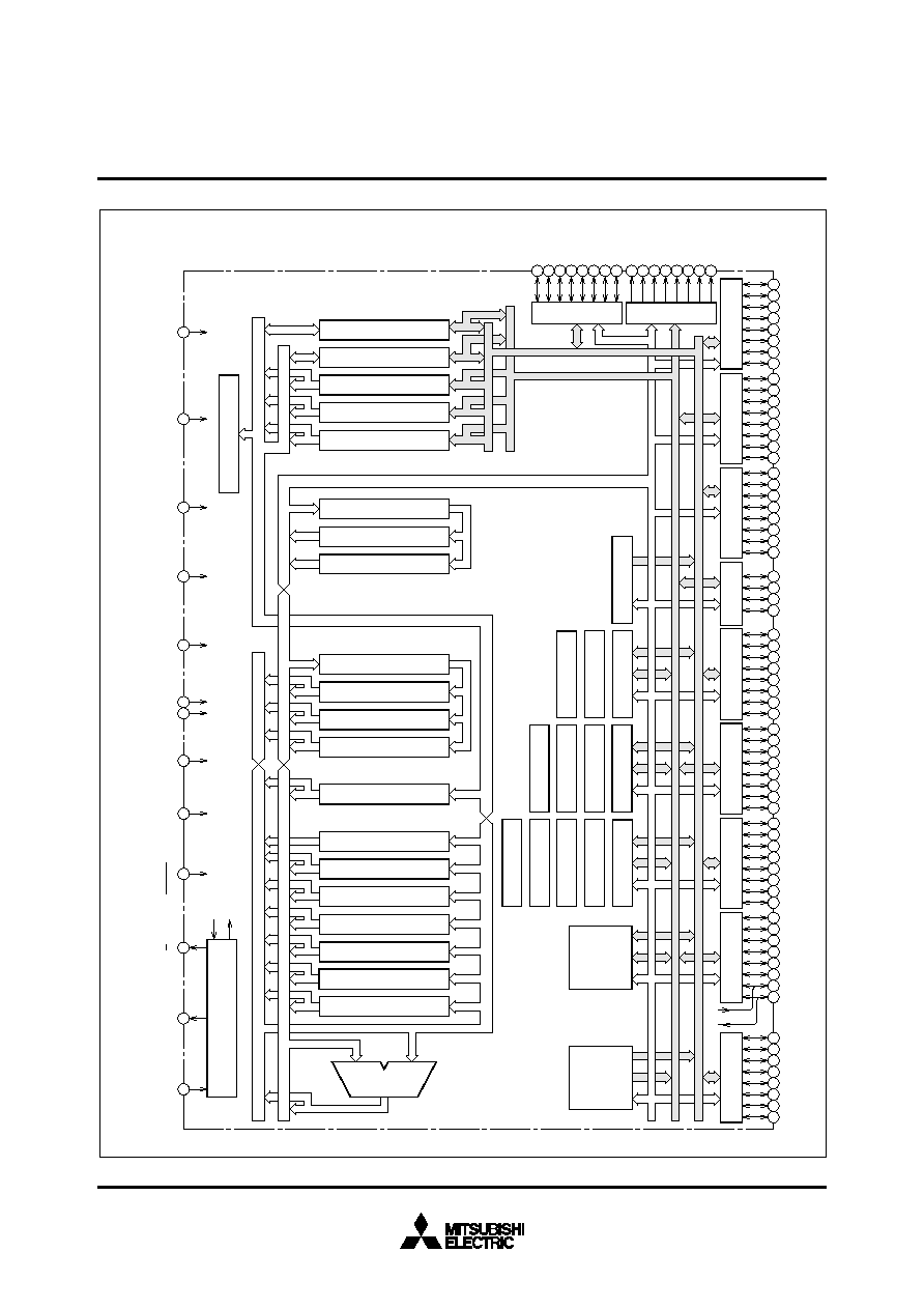
M37736EHLXXXHP BLOCK DIAGRAM
Clock input
X
IN
Clock output
X
OUT
Clock Generating Circuit
Timer TA4(16)
RAM
3968 bytes
PROM
124 Kbytes
Timer TA3(16)
Timer TA2(16)
Timer TA1(16)
P8(8)
Input/Output
port P8
P7(8)
Input/Output
port P7
X
CIN
X
COUT
P6(8)
Input/Output
port P6
P5(8)
Input/Output
port P5
P4(8)
Input/Output
port P4
P3(4)
Input/Output
port P3
P2(8)
Input/Output
port P2
P1(8)
Input/Output
port P1
P0(8)
Input/Output
port P0
Timer TA0(16)
Watchdog Timer
Timer TB2(16)
Timer TB1(16)
Timer TB0(16)
UART2(9)
UART1(9)
UART0(9)
A-D Converter(10)
Instruction Register(8)
Data Buffer DB
H
(8)
Data Buffer DB
L
(8)
Processor Status Register PS(11)
Direct Page Register DPR(16)
Stack Pointer S(16)
Index Register Y(16)
Index Register X(16)
Accumulator B(16)
Arithmetic Logic
Unit(16)
Accumulator A(16)
Instruction Queue Buffer Q
0
(8)
Instruction Queue Buffer Q
1
(8)
Incrementer(24)
Program Address Register PA(24)
Data Address Register DA(24)
Instruction Queue Buffer Q
2
(8)
Program Counter PC(16)
Incrementer/Decrementer(24)
Program Bank Register PG(8)
Data Bank Register DT((8)
Input Buffer Register IB(16)
Address Bus
Data Bus(Even)
Data Bus(Odd)
X
CIN
X
COUT
Enable output
E
Reset input
RESET
(0V)
V
SS
(0V)
AV
SS
CNV
SS
AV
CC
Reference
voltage input
V
REF
Bus method
selection input
BSEL
External data bus width
selection input
BYTE
V
CC
P9(8)
Output
port P9
P10(8)
Input/Output
port P10

MITSUBISHI MICROCOMPUTERS
M37736EHLXXXHP
PROM VERSION OF M37736MHLXXXHP
3
PRELIMINARY
Notice: This is not a final specification.
Some parametric limits are subject to change.
Parameter
Functions
Number of basic instructions
103
Instruction execution time
333 ns (the fastest instruction at external clock 12 MHz frequency)
PROM
124 Kbytes
RAM
3968 bytes
P0 ≠ P2, P4 ≠ P8, P10
8-bit
!
9
P3
4-bit
!
1
Output port
P9
8-bit
!
1
TA0, TA1, TA2, TA3, TA4
16-bit
!
5
TB0, TB1, TB2
16-bit
!
3
Serial I/O
(UART or clock synchronous serial I/O)
!
3
A-D converter
10-bit
!
1 (8 channels)
Watchdog timer
12-bit
!
1
3 external types, 16 internal types
Each interrupt can be set to the priority level (0 ≠ 7.)
2 circuits built-in (externally connected to a ceramic resonator or a
quartz-crystal oscillator)
Supply voltage
2.7 ≠ 5.5 V
9 mW (at 3 V supply voltage, external clock 12 MHz frequency)
22.5 mW (at 5 V supply voltage, external clock 12 MHz frequency)
Input/Output voltage
5 V
Output current
5 mA
External bus mode A; maximum 16 Mbytes,
External bus mode B; maximum 1 Mbytes
Operating temperature range
≠40 to 85 ∞C
Device structure
CMOS high-performance silicon gate process
Package
100-pin plastic molded fine-pitch QFP (100P6Q-A;0.5 mm lead pitch)
FUNCTIONS OF M37736EHLXXXHP
Memory size
Input/Output ports
Multi-function timers
Interrupts
Clock generating circuit
Power dissipation
Input/Output characteristic
Memory expansion
PRELIMINARY
Notice: This is not a final specification.
Some parametric limits are subject to change.
4
PROM VERSION OF M37736MHLXXXHP
MITSUBISHI MICROCOMPUTERS
M37736EHLXXXHP
Pin
Name
Input/Output
Functions
Vcc,
Power source
Apply 2.7 ≠ 5.5 V to Vcc and 0 V to Vss.
Vss
CNVss
CNVss input
Input
This pin controls the processor mode. Connect to Vss for the single-chip mode and the memory
expansion mode, and to Vcc for the microprocessor mode.
________
RESET
Reset input
Input
When "L" level is applied to this pin, the microcomputer enters the reset state.
These are pins of main-clock generating circuit. Connect a ceramic resonator or a quartz-
crystal oscillator between X
IN
and X
OUT
. When an external clock is used, the clock source should
be connected to the X
IN
pin, and the X
OUT
pin should be left open.
_
E
Enable output
Output
This pin functions as the enable signal output pin which indicates the access status in the internal
bus. In the external bus mode B and the memory expansion mode or the microprocessor mode,
___
this pin output signal
RDE
.
BYTE
External data
Input
In the memory expansion mode or the microprocessor mode, this pin determines whether the
bus width
external data bus has an 8-bit width or a 16-bit width. The data bus has a 16-bit width when "L"
selection input
signal is input and an 8-bit width when "H" signal is input.
BSEL
Bus method
Input
In the memory expansion mode or the microprocessor mode, this pin determines the external bus
select input
mode. The bus mode becomes the external bus mode A when "H" signal is input, and the external
bus mode B when "L" signal is input.
AVcc,
Analog power
Power source input pin for the A-D converter. Externally connect AVcc to Vcc and AVss to Vss.
AVss
source input
V
REF
Reference
Input
This is reference voltage input pin for the A-D converter.
voltage input
P0
0
≠ P0
7
I/O port P0
I/O
In the single-chip mode, port P0 becomes an 8-bit I/O port. An I/O direction register is available so
that each pin can be programmed for input or output. These ports are in the input mode when
reset.
In the memory expansion mode or the microprocessor mode, these pins output address (A
0
≠ A
7
)
___
___
____
at the external bus mode A, and these pins output signals
CS
0
≠
CS
4
and
RSMP
, and addresses
(A
16
, A
17
) at the external bus mode B.
P1
0
≠ P1
7
I/O port P1
I/O
In the single-chip mode, these pins have the same functions as port P0. When the BYTE pin is set
to "L" in the memory expansion mode or the microprocessor mode and external data bus has a
16-bit width, high-order data (D
8
≠ D
15
) is input/output or an address (A
8
≠ A
15
) is output. When
the BYTE pin is "H" and an external data bus has an 8-bit width, only address (A
8
≠ A
15
) is output.
P2
0
≠ P2
7
I/O port P2
I/O
In the single-chip mode, these pins have the same functions as port P0. In the memory expansion
mode or the microprocessor mode, low-order data (D
0
≠ D
7
) is input/output or an address
is output. When using the external bus mode A, the address is A
16
≠ A
23
. When using the
external bus mode B, the address is A
0
≠ A
7
.
P3
0
≠ P3
3
I/O port P3
I/O
In the single-chip mode, these pins have the same function as port P0. In the memory expansion
_
_
_
_
_
_
_
_
_
_
_
_
_
_
_
_
_
_
_
_
_
_
_
_
_
_
_
_
_
_
_
_
_
_
_
_
_
_
_
_
mode or the microprocessor mode, R/
W
,
BHE
, ALE, and
HLDA
signals are output at the external
________
____________
_________________
bus mode A, and
WEL
,
WEH
, ALE, and
HLDA
signals are output at the external bus mode B.
P4
0
≠ P4
7
I/O port P4
I/O
In the single-chip mode, these pins have the same functions as port P0. In the memory expansion
____
___
mode or the microprocessor mode, P4
0
, P4
1
, and P4
2
become
HOLD
and
RDY
input pins, and a
clock
1
output pin, respectively. Functions of the other pins are the same as in the single-chip
mode. However, in the memory expansion mode, P4
2
can be selected as an I/O port.
P5
0
≠ P5
7
I/O port P5
I/O
In addition to having the same functions as port P0 in the single-chip mode, these pins also
function as I/O pins for timers A0 to A3.
P6
0
≠ P6
7
I/O port P6
I/O
In addition to having the same functions as port P0 in the single-chip mode, these pins also
___
___
function as I/O pins for timer A4, input pins for external interrupt input (
INT
0
≠
INT
2
) and input pins
for timers B0 to B2. P6
7
also functions as sub-clock
SUB
output pin.
P7
0
≠ P7
7
I/O port P7
I/O
In addition to having the same functions as port P0 in the single-chip mode, these pins function
as input pins for A-D converter. Additionally, P7
6
and P7
7
have the function as the output pin
(X
COUT
) and the input pin (X
CIN
) of the sub-clock (32 kHz) oscillation circuit, respectively. When
P7
6
and P7
7
are used as the X
COUT
and X
CIN
pins, connect a resonator or an oscillator between
the both.
P8
0
≠ P8
7
I/O port P8
I/O
In addition to having the same functions as port P0 in the single-chip mode, these pins also
function as I/O pins for UART 0 and UART 1.
P9
0
≠ P9
7
Output port P9
Output
Port P9 is an 8-bit I/O port. These ports are floating when reset. When writing to the port latch,
these ports become the output mode. P9
0
≠ P9
3
also function as I/O port for UART 2.
P10
0
≠ P10
7
I/O port P10
I/O
In addition to having the same functions as port P0 in the single-chip mode. P10
4
≠ P10
7
also
_______
__
function as input pins for key input interrupt input (
Kl
0
≠
Kl
3
).
EVL0, EVL1
Output
These pins should be left open.
PIN DESCRIPTION
X
IN
Clock input
Input
X
OUT
Clock output
Output

MITSUBISHI MICROCOMPUTERS
M37736EHLXXXHP
PROM VERSION OF M37736MHLXXXHP
5
PRELIMINARY
Notice: This is not a final specification.
Some parametric limits are subject to change.
BASIC FUNCTION BLOCKS
The M37736EHLXXXHP has the same functions as the
M37736MHBXXXGP except for the following :
(1) The built-in ROM is PROM.
(2) The package is different.
(3) The reset circuit is different.
Refer to the section on the M37736MHBXXXGP.
RESET CIRCUIT
_____
The microcomputer is released from the reset state when the
RESET
pin is returned to "H" level after holding it at "L" level with the power
source voltage at 2.7 ≠ 5.5 V. Program execution starts at the address
formed by setting address A
23
≠ A
16
to 00
16
, A
15
≠ A
8
to the contents
of address FFFF
16
, and A
7
≠ A
0
to the contents of address FFFE
16
.
Figure 1 shows an example of a reset circuit. When the stabilized
clock is input from the external to the main-clock oscillation circuit,
the reset input voltage must be 0.55 V or less when the power source
voltage reaches 2.7 V. When a resonator/oscillator is connected to
the main-clock oscillation circuit, change the reset input voltage from
"L" to "H" after the main-clock oscillation is fully stabilized.
The status of the internal registers during reset is the same as the
M37736MHBXXXGP's.
Fig. 1 Example of a reset circuit
V
CC
RESET
RESET
V
CC
0V
0V
2.7V
0.55V
Power on
Note. In this case, stabilized clock is input from the
external to the main-clock oscillation circuit.
Perform careful evalvation at the system design
level before using.