MITSUMI
IC for Headphone Stereos LAG665
IC for Headphone Stereos
Monolithic IC LAG 665
Outline
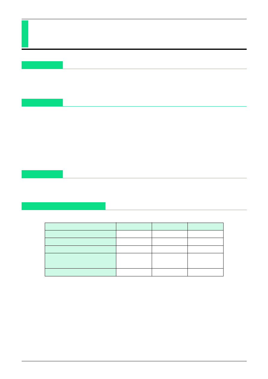
This IC was developed for use in headphone stereos, and incorporates dual preamp, power amp, electronic
VR and motor control circuits. It can be used in a simple circuit configuration which requires very few external
components.
Features
Package
Absolute Maximum Ratings
1. Broad operating voltage range of 2.0 to 5.0 V (amp system operates to 1.8 V)
2. Few external components required
1. Internal equalizer resistance
2. Direct coupling of preamps, electronic VR, power amp
3. No need for output coupling capacitor
3. Well-balanced electronic VR, A-curve attenuation characteristic obtained with B-curve VR
4. Internal motor control circuit, with noise from motor driving unit suppressed
5. Provided with pin to turn off preamps
SOP-28B (LAG665F)
SDIP-30A (LAG665D)
Item
Symbol
Ratings
Units
Operating temperature
Topr
-20~+65
�
C
Storage temperature
Tstg
-40~+125
�
C
Power supply current
V
CC
-0.3~+7.5
V
Power consumption
Pd
450 (SOP-28B)
mW
750 (SDIP-30A)
Operating voltage
Vop
2.0~5.0
V
MITSUMI
IC for Headphone Stereos LAG665
Electrical Characteristics
(Except where noted otherwise, Ta=25
�C
)
Item
Symbol
Measurement conditions
Min.
Typ.
Max.
Units
Consumption current
I
CC
V
IN
=0V, IM=0mA
18
25
mA
Preamp unit (Ta=25
�C
)
Open-circuit gain
Gvo
Vo=-10dBm, R
L
=
72
dB
Closed-circuit gain
Gvc
Vo=-10dBm
40
42
44
dB
Maximum output voltage
Vom
THD=10%
0.45
0.6
Vrms
Total harmonic distortion ratio
THD
V
OUT
=400mVrms
0.05
0.5
%
Output noise voltage
Vno
V
IN
=0, Rg=2.2k BPF(30~20kHz)
150
300
�Vrms
Input impedance
Z
IN
V
OUT
=-10dBm
18
22
k
Crosstalk between channels
C.T
Rg=2.2k, V
OUT
=-10dBm
30
dB
Output voltage with preamp off
Vooff
V
IN
=100mVrms
-50
dB
Output resistance with preamp off
Rooff
10
k
Input resistance on pre off
Rioff
10
k
Measurement conditions
Unless noted otherwise, V
CC
=3.0 V, f=1 kHz.
The preamp off pin is left open
Attenuator unit (Ta=25
�
C)
Maximum input voltage
Vi max.
0.2
Vrms
Maximum attenuation
Va max.
Vcont=min.
66
dB
Attenuation error
Vaerr
Vcont=max.
0
dB
Input impedance
Z
IN
15
20
k
Control pin input resistance
Zicot
100
k
Measurement conditions
Unless noted otherwise, V
CC
=3.0 V, f=1 kHz, (R
L
=16
).
Power amp unit (Ta=25
�
C)
Voltage gain
Gv
P
OUT
=5mW
26
28
30
dB
Voltage gain difference between channels
Gv
Vcont=max.
0
3
dB
Maximum output power I
Pom1
THD=10%, R
L
=32
20
28
mW
Maximum output power II
Pom2
THD=10%, R
L
=16
30
mW
Total harmonic distortion ratio
THD
P
OUT
=5mW
0.2
2.0
%
Crosstalk between channels
C.T
P
OUT
=5mW
20
30
dB
Output noise voltage
Vn
Rg=2.2k, Vcont=min.
0.25
1.0
mVrms
Ripple rejection
RR
V
CC
=3V, 100Hz, 100mVp-p
34
40
dB
Noise of preamp + power amp
Vnto
V
IN
=0V, Rg=2.2k, Vcont=max.
6
9
mVrms
Measurement conditions
Unless noted otherwise, V
CC
=3.0 V, f=1 kHz,(R
L
=16
).
Motor control unit (Ta=25
�
C)
Consumption current
IMC
3.0
5.0
mA
Startup current
IMS
500
mA
Reference voltage
Vref
Between RML-ADJ pins
0.72
0.80
0.87
V
Reference voltage fluctuation I
Vref1
V
CC
between 2.1 and 5.0 V
*
0.05
%/V
Reference voltage fluctuation II
Vref2
I
M
between 25 and 250 mA
0.01
%/mA
Reference voltage fluctuation III
Vref3
Ta between -10 and 50�C
0.01
%/
�
C
Current coefficient
K
32
38
43
Current coefficient fluctuation I
K1
V
CC
between 2.1 and 5.0 V
0.5
%/V
Current coefficient fluctuation II
K2
I
M
between 25 and 250 mA
0.05
%/mA
Current coefficient fluctuation III
K3
Ta between -10 and 50�C
0.02
%/
�
C
Output voltage on forced on
VCEsa
I
M
=200mA, 14PIN=V
CC
0.6
V
Input resistance on forced on
Rion
5.6
k
Leakage current on forced off
IML
200
�A
Input resistance on forced off
Ricon
33
k
Measurement conditions
Unless noted otherwise, V
CC
=3.0, I
M
=100 mA, circuit constants as specified.
Motor: M25E-7 (Mitsumi model)
*
Voltage across pins 13 and 19 (motor pins) fluctuates.
MITSUMI
IC for Headphone Stereos LAG665
Block Diagram
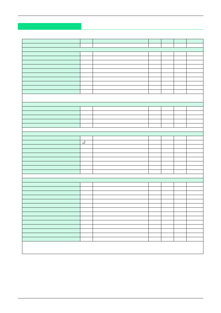
Measuring Circuit
MITSUMI
IC for Headphone Stereos LAG665
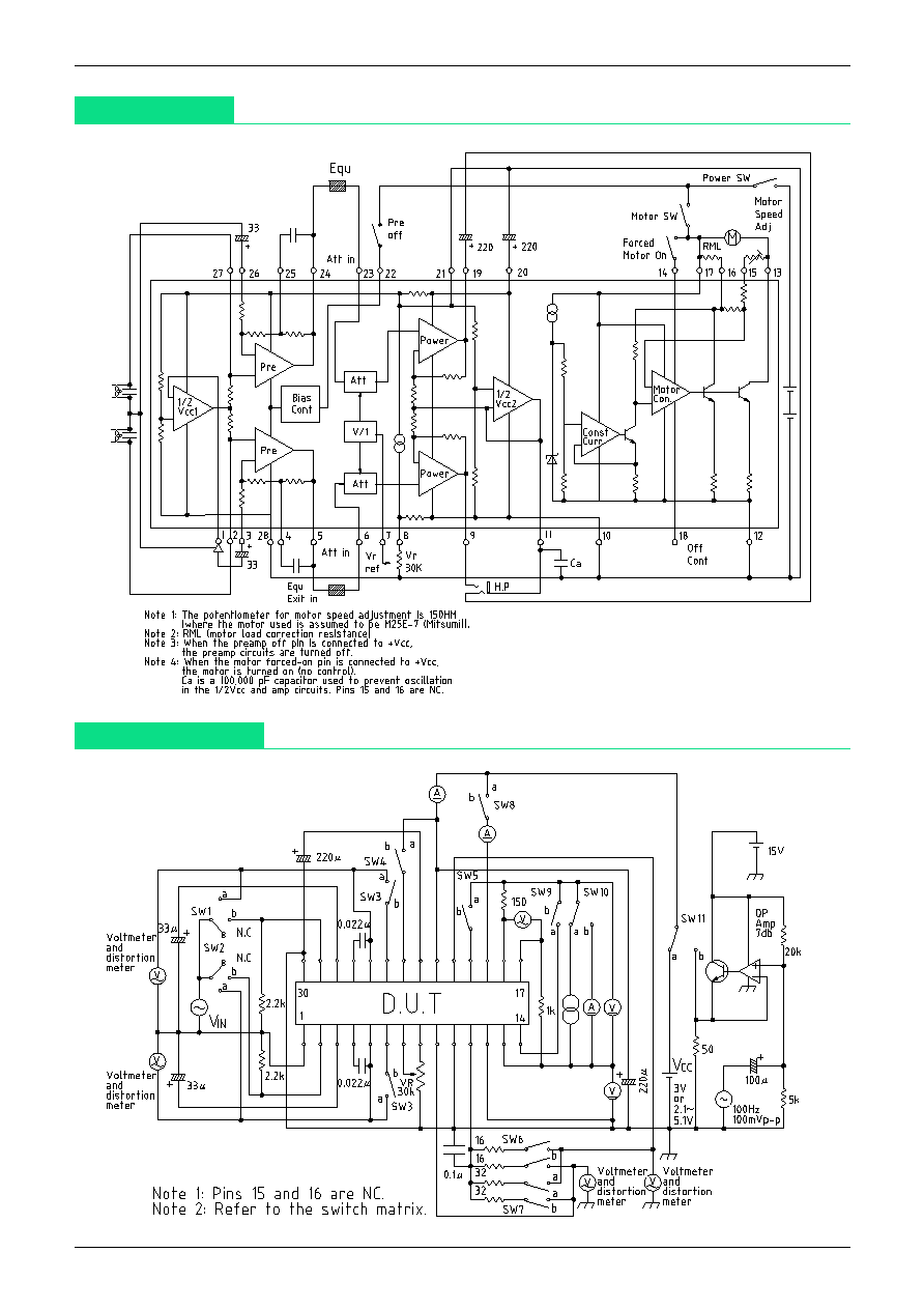
Switch Matrix
Switch Number
Conditions
Item
1
2
3
4
5
6
7
8
9 10 11
(Except where noted otherwise,
R
L
=16
, V
CC
=3V, Fosc=1kHz)
Consumption current
c
c
a
b
b
a
b
b
b
a
a
IM=0mA, VR=max.
Amp unit
Closed-circuit gain
b
b
b
Vo=-10dBm
Maximum output voltage
THD=10%
Total harmonic distortion ratio
Vo=400mVrms
Output noise voltage
c
c
Measured after inserting BPF (30 Hz to 20 kHz)
Preamp unit
b
VO=-10dBm, measured with channels swapped
Crosstalk between channels
using SW1, SW2
c
b
Output voltage with preamp off b
a
V
IN
=100mVrms
Maximum input voltage
a
a
a
V
IN
voltage when VR=mid, THD=10%
Maximum attenuation
Difference in V
O
output when VR=max and
Attenuator unit
output voltage when VR=min
Voltage gain
P
OUT
=5mW
Voltage gain difference
Channel output difference at VR=max
between channels
Maximum output power I
b
a
R
L
=32
, THD=10%
Maximum output power II
a
b
R
L
=16
, THD=10%
Power amp unit
Total harmonic distortion ratio
P
OUT
=5mW
Crosstalk between channels
c
P
OUT
=5mW measured with channels swapped
c
a
output voltage when VR=min
Output noise voltage
c
b
VR=min.
Ripple rejection
b
a
b
VR=max.
Pre + power noise
a
b
a
VR=max.
Consumption currentt
a
a
IM=0mA
Startup current
b
Reference voltage
a
IM=100mA (15~16PIN)
Reference voltage fluctuation I
IM=100mA, V
CC
=2.1~5.0V (13~17PIN)
Motor uni
Reference voltage fluctuation II
Vcc=3.0V, IM=25~250mA
Output voltage on forced on
a
IM=200mA
Leakage current on forced off
b
a
b
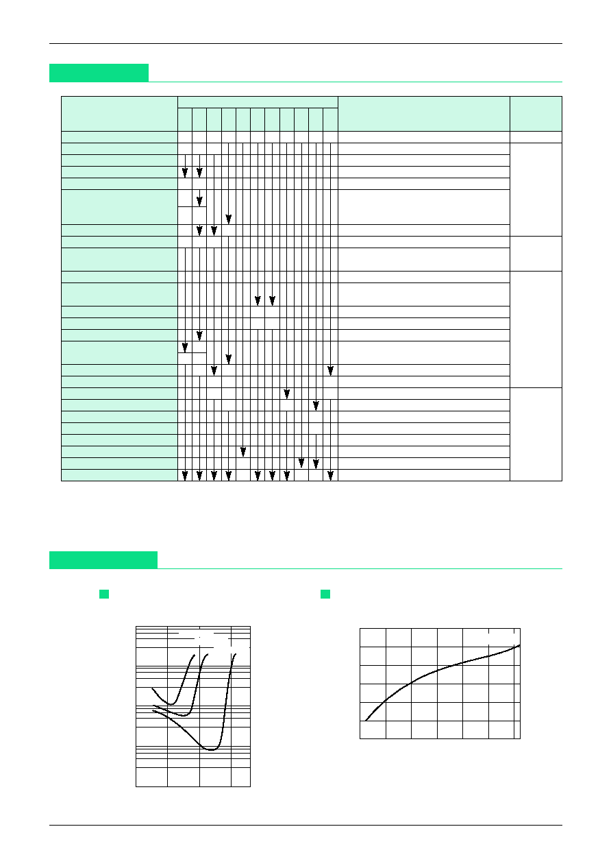
Characteristics
THD-V
OUT
10.0
1.0
0.1
0.01
-30
-20
-10
0
Output voltage (dBm)
V
CC
=1.8V
V
CC
=2.0V
V
CC
=3.0V
Total harmonic distortion ratio (%)
0/6
1/6
2/6
3/6
4/6
5/6
6/6
(min.)
(max.)
0
-20
-40
-60
-80
V
CC
=3.0V
V
ATT
-V
CONT
Output voltage attenuation (dB)
Voltage controllability
(B curve mechanical knob)
Preamp
Attenuator
Note: For switches with only on and off states, a = on and b = off.

MITSUMI
IC for Headphone Stereos LAG665
Power supply voltage
1.0
2.0
3.0
4.0
5.0
5
10
15
20
0
40
50
60
70
30
20
10
I
CC
-V
CC
R
L
=16
R
L
=32
I
OC
(R
L
=16
)
(THD=10%) P
OUT
max. (mW)
Power supply output
No-load consumption
current
(mA)
Power supply voltage (V)
1.0
2.0
3.0
4.0
5.0
0
-10
-20
-30
-40
-50
PREAMP OFF
V
R
=max.
Ripple rejection rate
-V
CC
F
R
=100Hz
V
R
=100mVrms
R
L
=16
Ripple rejection rate (dB)
100
-10
-20
-30
-40
-50
Frequency (Hz)
1k
10k
100k
V
CC
=3.0V
crosstalk frequency
Crosstalk (dB)
100
60
50
40
30
20
10
80
70
10
100
1k
10k
100k
Frequency (Hz)
V
CC
=3.0V
When V
R
=max.
TOTAL GAIN
POWER AMP GAIN
Gain (dB)
100
10
1
0.1
0.1
1
10
100
Power supply output (mW)
THD-P
OUT
V
CC
=1.8V
V
CC
=2.0V
V
CC
=3.0V
Total harmonic
distortion ratio (%)
P
OUT
. Power
amp
Power amp
Power amp
Voltage gain vs. frequency