MITSUMI
Remaining Battery Power Display MM1206
Remaining Battery Power Display
Monolithic IC MM1206
Outline
This IC detects battery voltage and displays the remaining power on an LED or LCD display. The appeal of
battery-driven equipment lies in its portability, but when the battery runs down and the equipment does not
function, customer complaints and breakdowns may result.
This IC prevents such trouble before it starts.
Features
1. There are three displays for remaining battery power :
FULL / MIDDLE / EMPTY.
2. Nine patterns built in for detection voltage, linked to two manganese batteries.
Standard setting : 2.5V, 2.25V
3. External parts held to a minimum
Package
SOP-8D (MM1206XF)
VSOP-8A (MM1206AF)
Detection Voltage Matrix Chart
*
Voltage Accuracy
Detection Voltage 1 : ±100mV typ.
Detection Voltage 2 : ±90mV typ.
SW1
SW2
Detection Voltage 1 Detection Voltage 2
GND
GND
2.64V
2.35V
GND
OPEN
2.62V
2.27V
GND
V
CC
2.60V
2.18V
OPEN
GND
2.52V
2.35V
OPEN
OPEN
2.50V
2.25V
OPEN
V
CC
2.48V
2.17V
V
CC
GND
2.42V
2.30V
V
CC
OPEN
2.40V
2.24V
V
CC
V
CC
2.38V
2.15V
Absolute Maximum Ratings
(Ta=25∞C)
Item
Rating
Storage temperature
-40~+125∞C
Operating temperature
-20~+70∞C
Input voltage
5V
Allowable loss
300mW
MITSUMI
Remaining Battery Power Display MM1206
Electrical Characteristics
(Unless otherwise specified Ta=25∞C, SW1=SW2=open)
Item
Symbol
Measurement Conditions
Min. Typ. Max. Unit.
Current consumption I
I
CC
V
CC
=3.0V
0.75
1.1
mA
Detection voltage I
V
TH
1
V
CC
=H L
2.4
2.5
2.6
V
Detection voltage II
V
TH
2
V
CC
=H L
2.16
2.25
2.34
V
Detection voltage difference
V
T
V
T
=V
TH
1-V
TH
2
210
250
290
mV
Detection voltage temperature factor
V
TH
/ T
±200
ppm/∞C
Detection voltage I, Adjustment 1
+ V
T
1
SW1=GND
70
100
130
mV
Detection voltage I, Adjustment 2
-
V
T
1
SW1=V
CC
-70
-100 -130
mV
Detection voltage II, Adjustment 1
+ V
T
2
SW2=GND
70
100
130
mV
Detection voltage II, Adjustment 2
-
V
T
2
SW2=V
CC
-70
-100 -130
mV
Output sink current I
I
S
1
V
CC
=2.7V, V
CE
=0.5V
5
10
mA
Output sink current II
I
S
2
V
CC
=2.38V, V
CE
=0.5V
5
10
mA
Output sink current III
I
S
3
V
CC
=2.0V, V
CE
=0.5V
5
10
mA
Output saturation voltage I
V
CE
1
V
CC
=2.7V, I
SINK
=1mA
100
150
mV
Output saturation voltage II
V
CE
2
V
CC
=2.38V, I
SINK
=1mA
100
150
mV
Output saturation voltage III
V
CE
3
V
CC
=2.0V, I
SINK
=1mA
50
80
mV
Output leak voltage I
I
LE
1
V
CC
=2.3V, V
CE
=1.5V
1
µA
Output leak voltage II
I
LE
2
V
CC
=2.7V, V
CE
=1.5V
1
µA
Output leak voltage II
I
LE
2'
V
CC
=2.0V, V
CE
=1.5V
1
µA
Output leak voltage III
I
LE
3
V
CC
=2.5V, V
CE
=1.5V
1
µA
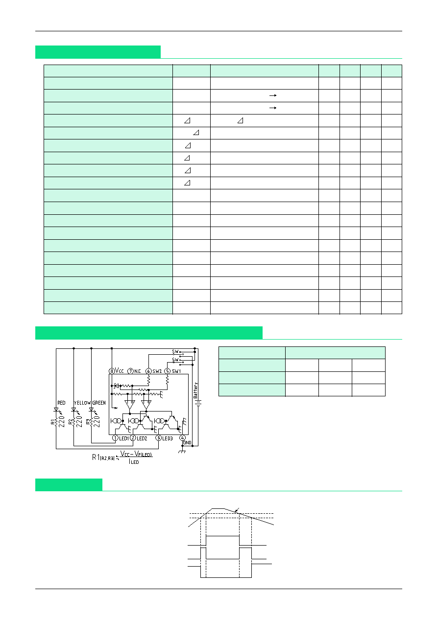
Block Diagram, Example of Application Circuit
2.50V 2.25V
LED1
ON
OFF
OFF
LED2
OFF
ON
OFF
LED3
OFF
OFF
ON
Timing Chart
V
CC
2.50V
2.25V
L E D 1
L E D 2
L E D 3
ON
OFF
ON
OFF
ON
OFF