
MITSUMI
3-Input 2-Output 3-Circuit Video Switch MM1238
3-Input 2-Output 3-Circuit Video Switch
Monolithic IC MM1238
Outline
This IC is a video switch developed for large and medium-sized high quality TVs, with 3-input and 2-output
circuits. It is suitable for BS, JSB, CS or M-N (Muse NTSC conversion) comparator switching. The BS-CS
decoder can be used as a W decoder.
Features
1. One of the two video signal outputs is for external output, and has a 6dB amp, 75
, 1V
P-P
2. Input impedance
Video circuits 1~3
15k
Audio circuits 1~3
68k
3. Crosstalk
Video
-60dB (at 4.43MHz)
Audio
-80dB (at 1kHz)
Video : Audio
-70dB (at 100kHz)
4. Frequency response
10MHz (6dB, 75
, amp only, 7MHz)
5. Power supply voltage
8.0V
~13.0V
Package
SDIP-22A (MM1238XD)
Applications
1. TV
2. Free-standing VCR
3. Other video equipment
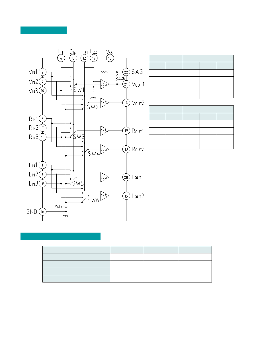
Pin Assignment
SDIP-22P
1
3
6
9
2
4 5
8
7
10 11
22
18
15
21
19
17 16
14
20
12
13
Pin no.
Pin name
Function
Pin no.
Pin name
Function
1
L
IN
1
Audio L
IN
1
12
C21
SW2 control
2
V
IN
1
Video IN1
13
R
OUT
2
Audio R
OUT
2
3
R
IN
1
Audio R
IN
1
14
V
OUT
2
Video OUT2
4
C11
SW1 control
15
L
OUT
2
Audio L
OUT
2
5
L
IN
2
Audio L
IN
2
16
GND
GND
6
V
IN
2
Video IN2
17
C22
SW2 control
7
R
IN
2
Audio R
IN
2
18
V
CC
Power supply
8
C12
SW1 control
19
R
OUT
1
Audio R
OUT
1
9
L
IN
3
Audio L
IN
3
20
L
OUT
1
Audio L
OUT
1
10
V
IN
3
Video IN3
21
V
OUT
1
Video OUT1
11
R
IN
3
Audio R
IN
3
22
SAG
Sag pin
MITSUMI
3-Input 2-Output 3-Circuit Video Switch MM1238
Block Diagram
Control input
Output signal
C11
C12
V
OUT
1
R
OUT
1
L
OUT
1
L
L
Mute
Mute
Mute
L
H
VIn1
RIn1
LIn1
H
L
VIn2
RIn2
LIn2
H
H
VIn3
RIn3
LIn3
Control input
Output signal
C21
C22
V
OUT
2
R
OUT
2
L
OUT
2
L
L
Mute
Mute
Mute
L
H
VIn1
RIn1
LIn1
H
L
VIn2
RIn2
LIn2
H
H
VIn3
RIn3
LIn3
SW Logic
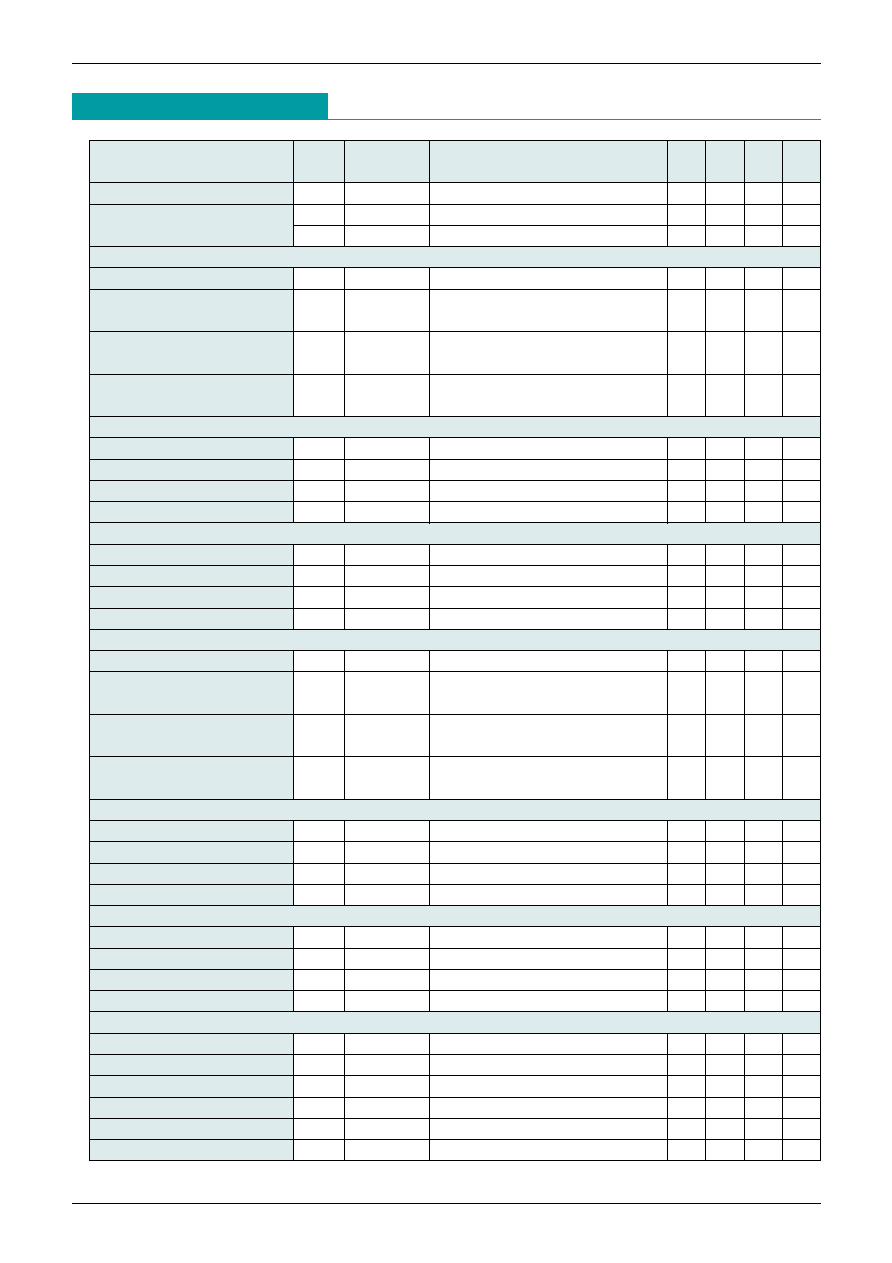
Absolute Maximum Ratings
(Ta=25�C)
Item
Symbol
Ratings
Units
Storage temperature
T
STG
-40~+125
�C
Operating temperature
T
OPR
-20~+75
�C
Power supply voltage
V
CC
15
V
Allowable loss
Pd
800
mW
MITSUMI
3-Input 2-Output 3-Circuit Video Switch MM1238
Electrical Characteristics
(Except where noted otherwise, Ta=25�C, V
CC
= 8V~13V)
Item
Symbol
Measurement
Measurement conditions
Min. Typ. Max. Units
circuit
Operating power supply voltage
V
CC
V
CC
8.0
13.0
V
Consumption current
I
CC
1
V
CC
=9V
22.0 29.0 mA
I
CC
2
V
CC
=12V
25.0 33.0 mA
V
OUT
1 output
Voltage gain
G
V
1
TP7
SG2 : Sine wave 1V
P-P
, 0.1MHz
5.7
6.2
6.7
dB
Frequency characteristic
F
V
1
TP7
SG2 : Sweep signal 1V
P-P
7MHz/0.1MHz
-1.0
0
1.0
dB
Differential gain
DG1
TP8
SG2 : Staircase wave 1V
P-P
APL=10, 50, 90%
0
3
%
Differential phase
DP1
TP8
SG2 : Staircase wave 1V
P-P
APL=10, 50, 90%
0
3
deg
R
OUT
1 output
Voltage gain
G
R
1
TP5
SG3 : Sine wave 2.5V
P-P
, 1kHz
-0.5
0
0.5
dB
Total harmonic distortion
THD
R
1
TP5
SG3 : Sine wave 2.5V
P-P
, 1kHz
0.01
0.1
%
Mute noise
V
NM
1
TP5
15kHz band during mute select
180
�Vrms
Output noise voltage
V
NR
1
TP5
15kHz band during pin select
3
50
�Vrms
L
OUT
1 output
Voltage gain
G
L
1
TP6
SG1 : Sine wave 2.5V
P-P
, 1kHz
-0.5
0
0.5
dB
Total harmonic distortion
THD
L
1
TP6
SG1 : Sine wave 2.5V
P-P
, 1kHz
0.01
0.1
%
Mute noise
V
NM
2
TP6
15kHz band during mute select
180
�Vrms
Output noise voltage
V
NL
1
TP6
15kHz band during pin select
3
50
�Vrms
V
OUT
2 output
Voltage gain
Gv2
TP2
SG2 : Sine wave 1V
P-P
, 0.1MHz
-0.5
0
0.5
dB
Frequency characteristic
Fv2
TP2
SG2 : Sweep signal 1V
P-P
10MHz/0.1MHz
-1.0
0
1.0
dB
Differential gain
DG2
TP3
SG2 : Staircase wave 1V
P-P
APL=10, 50, 90%
0
3
%
Differential phase
DP2
TP3
SG2 : Staircase wave 1V
P-P
APL=10, 50, 90%
0
3
deg
R
OUT
2 output
Voltage gain
G
R
2
TP1
SG3 : Sine wave 2.5V
P-P
, 1kHz
-0.5
0
0.5
dB
Total harmonic distortion
THD
R
2
TP1
SG3 : Sine wave 2.5V
P-P
, 1kHz
0.01
0.1
%
Mute noise
V
NM
3
TP1
15kHz band during mute select
180
�Vrms
Output noise voltage
V
NR
2
TP1
15kHz band during pin select
3
50
�Vrms
L
OUT
2 output
Voltage gain
G
L
2
TP4
SG1 : Sine wave 2.5V
P-P
, 1kHz
-0.5
0
0.5
dB
Total harmonic distortion
THD
L
2
TP4
SG1 : Sine wave 2.5V
P-P
, 1kHz
0.01
0.1
%
Mute noise
V
NM
4
TP4
15kHz band during mute select
180
�Vrms
Output noise voltage
V
NR
2
TP4
15kHz band during pin select
3
50
�Vrms
Output offset voltage
V
OUT
1
V
OFF
1
TP7
V
OUT
1 pin DC level difference during switching
0
�30
mV
V
OUT
2
V
OFF
2
TP2
V
OUT
2 pin DC level difference during switching
0
�15
mV
R
OUT
1
V
OFF
3
TP5
R
OUT
1 pin DC level difference during switching
0
�15
mV
R
OUT
2
V
OFF
4
TP1
R
OUT
2 pin DC level difference during switching
0
�15
mV
L
OUT
1
V
OFF
5
TP6
L
OUT
1 pin DC level difference during switching
0
�15
mV
L
OUT
2
V
OFF
6
TP4
L
OUT
2 pin DC level difference during switching
0
�15
mV

MITSUMI
3-Input 2-Output 3-Circuit Video Switch MM1238
Input impedance
V
IN
R
IV
V
IN
1~V
IN
3
15
k
R
IN
R
IR
R
IN
1~R
IN
3
68
k
L
IN
R
IL
L
IN
1~L
IN
3
68
k
Output impedance
V
OUT
V
OV
V
OUT
2
50
R
OUT
V
OR
R
OUT
1 and R
OUT
2
50
L
OUT
V
OL
L
OUT
1 and L
OUT
2
50
Crosstalk
V
IN
V
OUT
CT
VV
SG2 : 1V
P-P
, 4.43MHZ
*
1
-60
-50
dB
R
IN
R
OUT
CT
RR
SG3 : 2.5V
P-P
, 1kHZ
*
2
-80
-70
dB
L
IN
L
OUT
CT
LL
SG1 : 2.5V
P-P
, 1kHZ
*
3
-80
-70
dB
V
IN
R
OUT
CT
RV
SG2 : 1V
P-P
, 100kHz
*
4
-70
-60
dB
V
IN
L
OUT
CT
LV
SG2 : 1V
P-P
, 100kHz
*
5
-70
-60
dB
Switch input voltage
SW input voltage H
V
IH
Switching H level for each IC SW
2.1
V
SW input voltage L
V
IL
Switching L level for each IC SW
0.7
V
Input dynamic range
V
IN
V
OUT
D1
V
CC
=12V, SG1 : sine wave, 1kHz
2.6
V
P
-
P
V
CC
=12V, SG2 : sine wave, 1kHz
R
IN
R
OUT
D2
Total higher harmonic
2.0
Vrms
distortion=0.5%
V
CC
=12V, SG3 : sine wave, 1kHz
L
IN
L
OUT
D3
Total higher harmonic
2.0
Vrms
distortion=0.5%
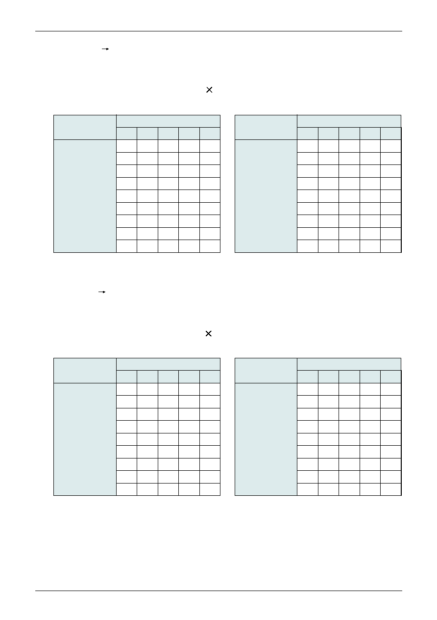
*
1 Crosstalk (V
IN
V
OUT
)
Input a 1V
P-P
, 4.43MHz sine wave to SG2.
Obtain C
TVV
using the following formula given output amplitude for combinations other than those below
for SW control pin as V
O
1, and for the combinations below as V
O
2.
C
TVV
=20 log (V
O
2/V
O
1) dB
1. C
TVV
1
Measuring pin
Switch status
S2
V1
V2
V3
V4
A
L
L
L
H
A
H
L
L
H
A
H
H
L
H
B
L
L
H
L
TP8
B
L
H
H
L
B
H
H
H
L
C
L
L
H
H
C
L
H
H
H
C
H
L
H
H
2. C
TVV
2
Measuring pin
Switch status
S2
V1
V2
V3
V4
A
L
H
L
L
A
L
H
H
L
A
L
H
H
H
B
H
L
L
L
TP3
B
H
L
L
H
B
H
L
H
H
C
H
H
L
L
C
H
H
L
H
C
H
H
H
L
MITSUMI
3-Input 2-Output 3-Circuit Video Switch MM1238
*
2 Crosstalk (R
IN
R
OUT
)
Input a 2.5V
P-P
, 1kHz sine wave to SG3.
Obtain C
TRR
using the following formula given output amplitude for combinations other than those below
for SW control pin as V
O
3, and for the combinations below as V
O
4.
C
TRR
=20 log (V
O
4/V
O
3) dB
1. C
TRR
1
Measuring pin
Switch status
S3
V1
V2
V3
V4
A
L
L
L
H
A
H
L
L
H
A
H
H
L
H
B
L
L
H
L
TP5
B
L
H
H
L
B
H
H
H
L
C
L
L
H
H
C
L
H
H
H
C
H
L
H
H
2. C
TRR
2
Measuring pin
Switch status
S3
V1
V2
V3
V4
A
L
H
L
L
A
L
H
H
L
A
L
H
H
H
B
H
L
L
L
TP1
B
H
L
L
H
B
H
L
H
H
C
H
H
L
L
C
H
H
L
H
C
H
H
H
L
*
3 Crosstalk (L
IN
L
OUT
)
Input a 2.5V
P-P
, 1kHz sine wave to SG3.
Obtain C
TLL
using the following formula given output amplitude for combinations other than those below
for SW control pin as V
O
5, and for the combinations below as V
O
6.
C
TLL
=20 log (V
O
6/V
O
5) dB
1. C
TLL
1
Measuring pin
Switch status
S1
V1
V2
V3
V4
A
L
L
L
H
A
H
L
L
H
A
H
H
L
H
B
L
L
H
L
TP6
B
L
H
H
L
B
H
H
H
L
C
L
L
H
H
C
L
H
H
H
C
H
L
H
H
2. C
TLL
2
Measuring pin
Switch status
S1
V1
V2
V3
V4
A
L
H
L
L
A
L
H
H
L
A
L
H
H
H
B
H
L
L
L
TP4
B
H
L
L
H
B
H
L
H
H
C
H
H
L
L
C
H
H
L
H
C
H
H
H
L

MITSUMI
3-Input 2-Output 3-Circuit Video Switch MM1238
*
4 Crosstalk (V
IN
-R
OUT
, L
OUT
)
Input a 1Vp-p, 100kHz sine wave to SG2.
Obtain C
TRV
(C
TLV
) using the following formula given output amplitude for combinations other than those
below for SW control pin as V
O
7, and for the combinations below as V
O
8.
C
TRV
(C
TLV
)=20 log (V
O
8/V
O
7) dB
1. C
TRV
Measuring pin
Switch status
S2
V1
V2
V3
V4
A
L
H
L
H
TP5
B
H
L
H
L
C
H
H
H
H
A
L
H
L
H
TP1
B
H
L
H
L
C
H
H
H
H
2. C
TLV
Measuring pin
Switch status
S2
V1
V2
V3
V4
A
L
H
L
H
TP6
B
H
L
H
L
C
H
H
H
H
A
L
H
L
H
TP4
B
H
L
H
L
C
H
H
H
H
Measuring Circuit