 | –≠–ª–µ–∫—Ç—Ä–æ–Ω–Ω—ã–π –∫–æ–º–ø–æ–Ω–µ–Ω—Ç: PST3457 | –°–∫–∞—á–∞—Ç—å:  PDF PDF  ZIP ZIP |

MITSUMI
CMOS System Reset PST3XXX
CMOS System Reset
Monolithic IC PST3XXX Series
Outline
This IC is a system reset IC developed using the CMOS process. Super low consumption current of 0.25µA
typ. has been achieved through use of the CMOS process. Also, detection voltage is high precision detection
of ±2%.
Features
(1) Super low consumption current
0.25µA typ. (when V
DD
= Vs + 1V)
(2) High precision detection voltage
±2%
(3) Hysteresis characteristic
5% typ.
(4) Operating range
0.95 ~ 10V
(5) Wide operating temperature range
-30 ~ +85∞C
(6) Detection voltage
2 ~ 6V (0.1V step)
Package
SC-82AB (PST31XX, PST32XX)
SOT-25 (PST33XX, PST34XX)
Applications
(1) Microcomputer, CPU, MPU reset circuits
(2) Logic circuit reset circuits
(3) Battery voltage check circuits
(4) Back-up circuit switching circuits
(5) Level detection circuits
Pin Assignment
1
3
5
2
4
SC-82AB
1
2
4
3
SOT-25
1
OUT
2
V
DD
3
V
SS
4
NC
5
1
OUT
2
V
DD
3
NC
4
V
SS
MITSUMI
CMOS System Reset PST3XXX
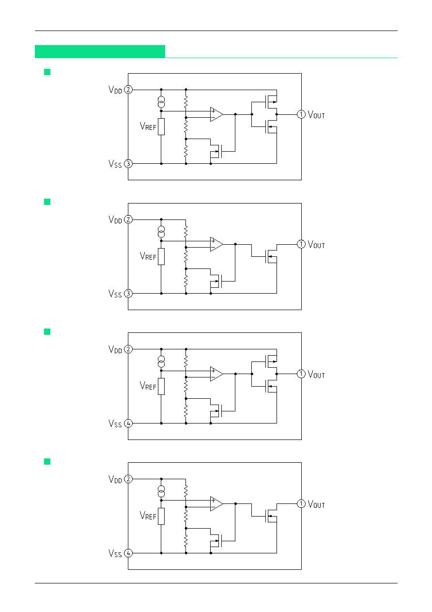
Equivalent Circuit Diagram
PST31XX
PST32XX
PST33XX
PST34XX
MITSUMI
CMOS System Reset PST3XXX
Absolute Maximum Ratings
(Ta=25∞C)
Electrical Characteristics
Item
Symbol
Rating
Unit
Storage temperature
T
STG
-40~+125
∞C
Operating temperature
T
OPR
-30~+85
∞C
Power supply voltage
V
DD
max.
+12
V
Allowable loss
Pd
150
mW
Detection voltage
SOT-25
SC-82
CMOS output
N-ch open drain
CMOS output
N-ch open drain
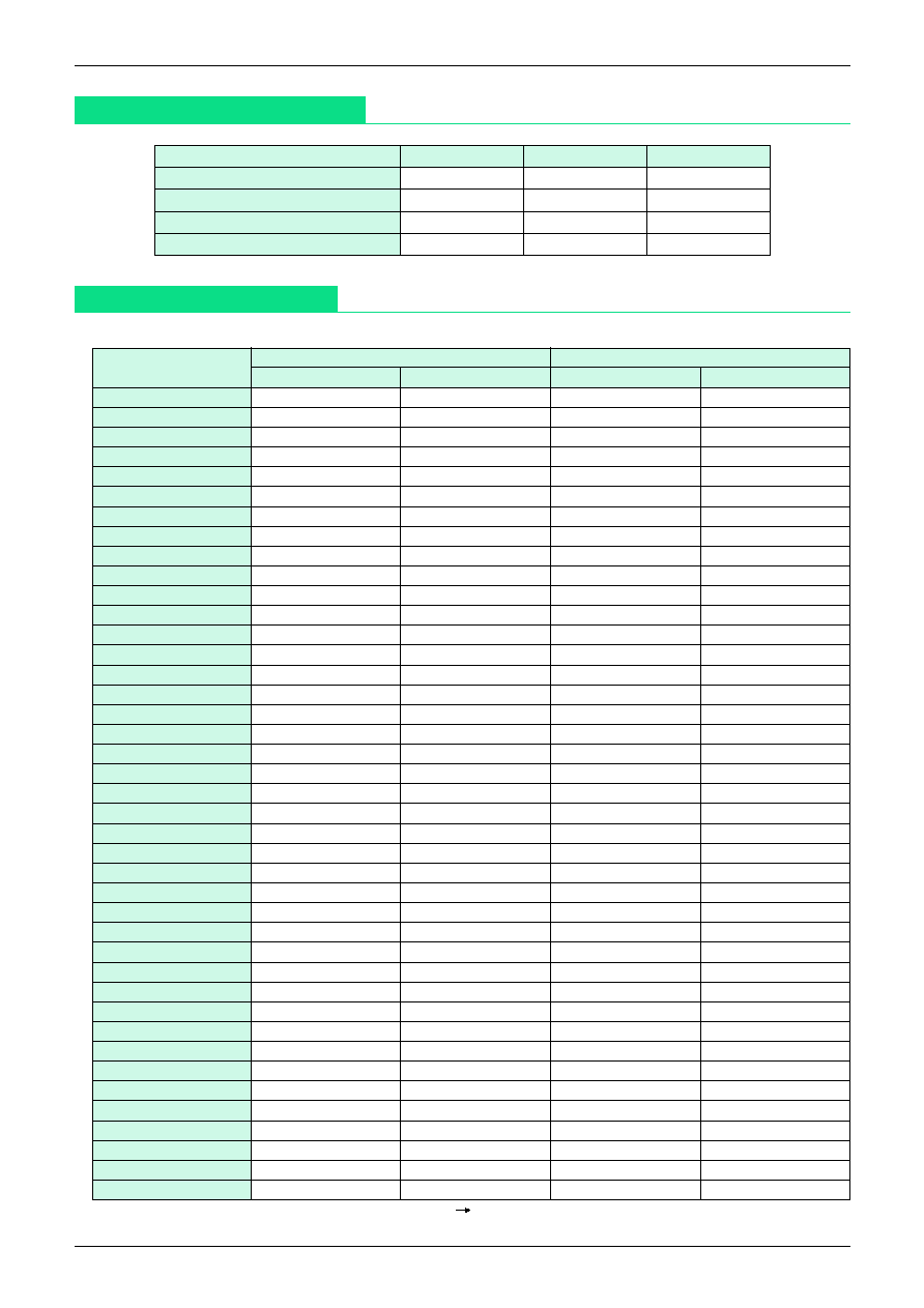
2.0V±2%
PST3120
PST3220
PST3320
PST3420
2.1V±2%
PST3121
PST3221
PST3321
PST3421
2.2V±2%
PST3122
PST3222
PST3322
PST3422
2.3V±2%
PST3123
PST3223
PST3323
PST3423
2.4V±2%
PST3124
PST3224
PST3324
PST3424
2.5V±2%
PST3125
PST3225
PST3325
PST3425
2.6V±2%
PST3126
PST3226
PST3326
PST3426
2.7V±2%
PST3127
PST3227
PST3327
PST3427
2.8V±2%
PST3128
PST3228
PST3328
PST3428
2.9V±2%
PST3129
PST3229
PST3329
PST3429
3.0V±2%
PST3130
PST3230
PST3330
PST3430
3.1V±2%
PST3131
PST3231
PST3331
PST3431
3.2V±2%
PST3132
PST3232
PST3332
PST3432
3.3V±2%
PST3133
PST3233
PST3333
PST3433
3.4V±2%
PST3134
PST3234
PST3334
PST3434
3.5V±2%
PST3135
PST3235
PST3335
PST3435
3.6V±2%
PST3136
PST3236
PST3336
PST3436
3.7V±2%
PST3137
PST3237
PST3337
PST3437
3.8V±2%
PST3138
PST3238
PST3338
PST3438
3.9V±2%
PST3139
PST3239
PST3339
PST3439
4.0V±2%
PST3140
PST3240
PST3340
PST3440
4.1V±2%
PST3141
PST3241
PST3341
PST3441
4.2V±2%
PST3142
PST3242
PST3342
PST3442
4.3V±2%
PST3143
PST3243
PST3343
PST3443
4.4V±2%
PST3144
PST3244
PST3344
PST3444
4.5V±2%
PST3145
PST3245
PST3345
PST3445
4.6V±2%
PST3146
PST3246
PST3346
PST3446
4.7V±2%
PST3147
PST3247
PST3347
PST3447
4.8V±2%
PST3148
PST3248
PST3348
PST3448
4.9V±2%
PST3149
PST3249
PST3349
PST3449
5.0V±2%
PST3150
PST3250
PST3350
PST3450
5.1V±2%
PST3151
PST3251
PST3351
PST3451
5.2V±2%
PST3152
PST3252
PST3352
PST3452
5.3V±2%
PST3153
PST3253
PST3353
PST3453
5.4V±2%
PST3154
PST3254
PST3354
PST3454
5.5V±2%
PST3155
PST3255
PST3355
PST3455
5.6V±2%
PST3156
PST3256
PST3356
PST3456
5.7V±2%
PST3157
PST3257
PST3357
PST3457
5.8V±2%
PST3158
PST3258
PST3358
PST3458
5.9V±2%
PST3159
PST3259
PST3359
PST3459
6.0V±2%
PST3160
PST3260
PST3360
PST3460
Detection voltage measurement conditions: V
DD
= 9V 0V, measurement circuit 1
(1) Detection Voltage Table Ta=25∞C
MITSUMI
CMOS System Reset PST3XXX
Electrical Characteristics
(Except where noted otherwise, Ta=25∞C)
Measuring Circuit
Item
Symbol
Measurement
Measurement conditions
Min.
Typ.
Max.
Unit
circuit
Hysteresis voltage
Vs
1
Vs 0.03 Vs 0.05 Vs 0.08
V
Detection voltage
temperature coefficient
Vs/ T
1
Ta=-30~+85∞C
±0.01
%/∞C
Consumption current
I
CC
1
V
DD
=Vs+1V
*
1
0.25
1
µA
N-ch output current 1
2
V
DD
=1.2V,
Nch : V
DS
=0.5V
0.23
0.5
mA
N-ch output current 2
2
V
DD
=2.4V,
Nch : V
DS
=0.5V,Vs>2.5V
*
1
1.6
3.7
mA
N-ch output current 3
2
V
DD
=3.6V,
Nch : V
DS
=0.5V,Vs>3.7V
*
1
3.2
7.0
mA
P-ch output current 1
*
2
3
V
DD
=4.8V,
Pch : V
DS
=0.5V,Vs<4.7V
*
1
0.36
0.62
mA
P-ch output current 2
*
2
3
V
DD
=6.0V,
Pch : V
DS
=0.5V,Vs<5.9V
*
1
0.46
0.75
mA
Notes:
*
1 Vs is detection voltage
*
2 Only for CMOS output products
Measuring Circuit 1
Measuring Circuit 3
Measuring Circuit 2
R
L
is not needed for CMOS output.
MITSUMI
CMOS System Reset PST3XXX
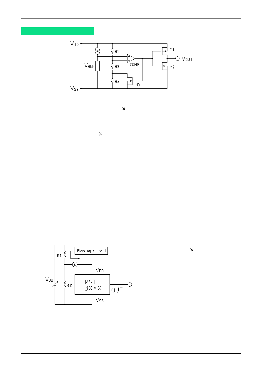
Description of Operation
(1) V
DD
> VS, V
OUT
: H (M1: ON, M2, M3: OFF)
When V
DD
is gradually lowered from the above state, detection voltage is as follows.
Detection voltage: (R1 + R2 + R3) / (R2 + R3) VREF
(2) V
DD
< VS, V
OUT
: L (M1: OFF, M2, M3: ON)
When V
DD
is gradually raised from the above state, release voltage is as follows.
Release voltage = (R1 + R2) / (R2) VREF
(3) Hysteresis voltage = (release voltage) - (detection voltage).
(4) When V
DD
drops and goes below the minimum operating voltage, output is undefined; when output is
pulled up, output becomes V
DD
.
(5) VREF and detection resistors
1) The reference voltage source (VREF) for this IC is 0.8V typ. This gives excellent low power consumption
and temperature characteristics.
2) The high resistance process is used for resistors R1, R2 and R3 to achieve low consumption current for
the IC.
(6) Through current flows momentarily for detection and release. When using high V
DD
pin impedance, the
through current may cause oscillation.
(Example) Detection voltage changed by external settings
*
The IC input voltage fluctuates due to the
through current R11 voltage drop, and
an oscillation state where detection and
release are repeated may occur.
*
With CMOS output types, do not use as
shown in the diagram at left.
MITSUMI
CMOS System Reset PST3XXX
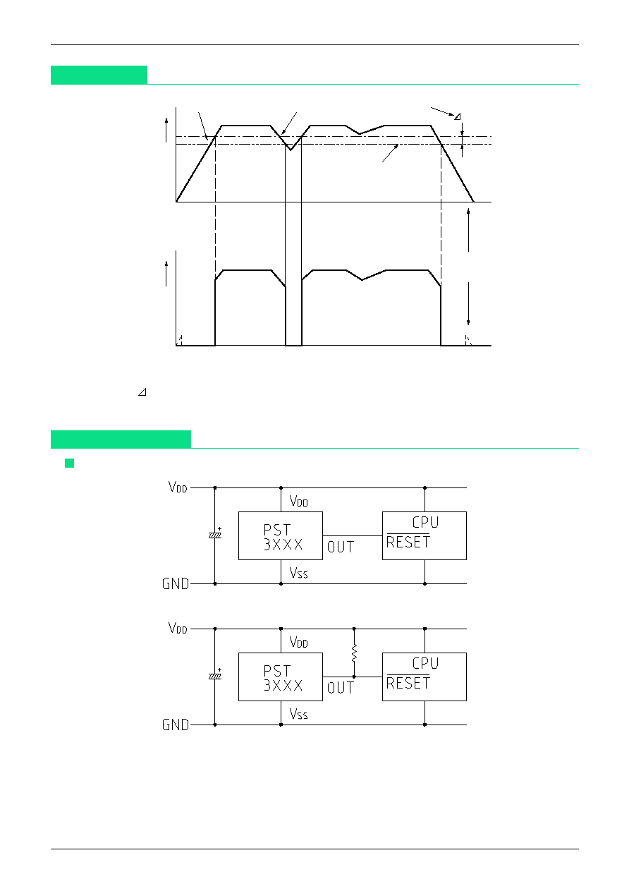
Timing Chart
(2)
V
DD
V
OUT
V
V
(1)
(3)
(4)
V
S
V
S
(1) ~ (4) in the above diagram correspond to the Description of Operation.
Vs detection voltage
Vs hysteresis voltage
PST31XX, PST33XX (CMOS output products)
Application Circuits
Normal reset circuit
PST32XX, PST34XX (N-ch open drain output products)
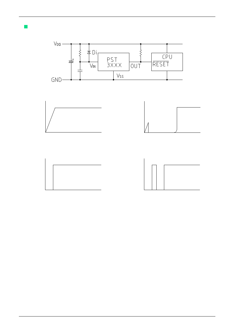
MITSUMI
CMOS System Reset PST3XXX
PST32XX, PST34XX (N-ch open drain output products)
If there is a problem with delay in rise time, insert a Di.
Power ON reset circuit
T (S)
V
DD
(V)
T (S)
OUT (V)
If power supply rises suddenly, output may go "H" momentarily when below minimum operating
voltage (0.95V), as shown in the above diagram.
T(S)
V
DD
(V)
T (S)
OUT (V)
A power ON reset circuit can be configured on PST32XX, PST34XX (N-ch open drain output products).
MITSUMI
CMOS System Reset PST3XXX
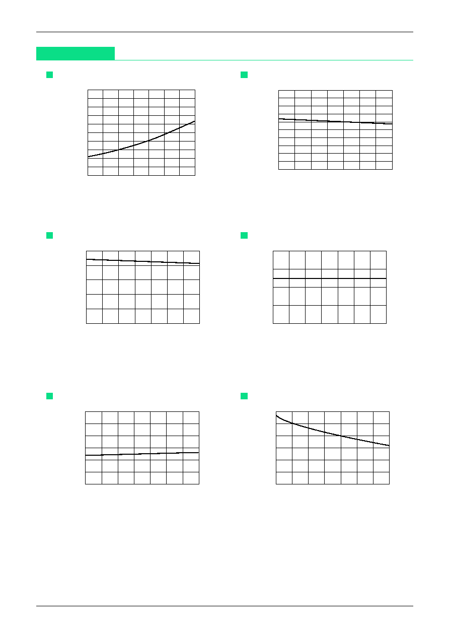
Characteristics
(For products with PST3128 detection voltage 2.8V typ.)
Consumption current (V
DD
= 3.8V) temperature
0
-40
100
80
40
60
20
0
-20
Consumption current (
µ
A)
Temperature (
∞
C)
0.5
0.4
0.45
0.35
0.3
0.25
0.2
0.15
0.1
0.05
Detection voltage temperature
2.5
-40
100
80
40
60
20
0
-20
Detection voltage (V)
Temperature (
∞
C)
2.9
2.95
2.85
2.8
2.75
2.7
2.65
2.6
2.55
3
Release voltage temperature
2.5
-40
100
80
40
60
20
0
-20
Release voltage (V)
Temperature (
∞
C)
2.8
2.9
2.7
2.6
3
Hysteresis voltage temperature
0
-40
100
80
40
60
20
0
-20
Hysteresis voltage (mV)
Temperature (
∞
C)
100
150
50
200
N-ch output current temperature (V
DS
= 0.5V)
0
-40
100
80
40
60
20
0
-20
N-ch output current (mA)
Temperature (
∞
C)
1.5
2.5
2
1
0.5
3
P-ch output current temperature (V
DS
= 0.5V)
0
-40
100
80
40
60
20
0
-20
P-ch output current (mA)
Temperature (
∞
C)
1.5
2.5
2
1
0.5
3
MITSUMI
CMOS System Reset PST3XXX
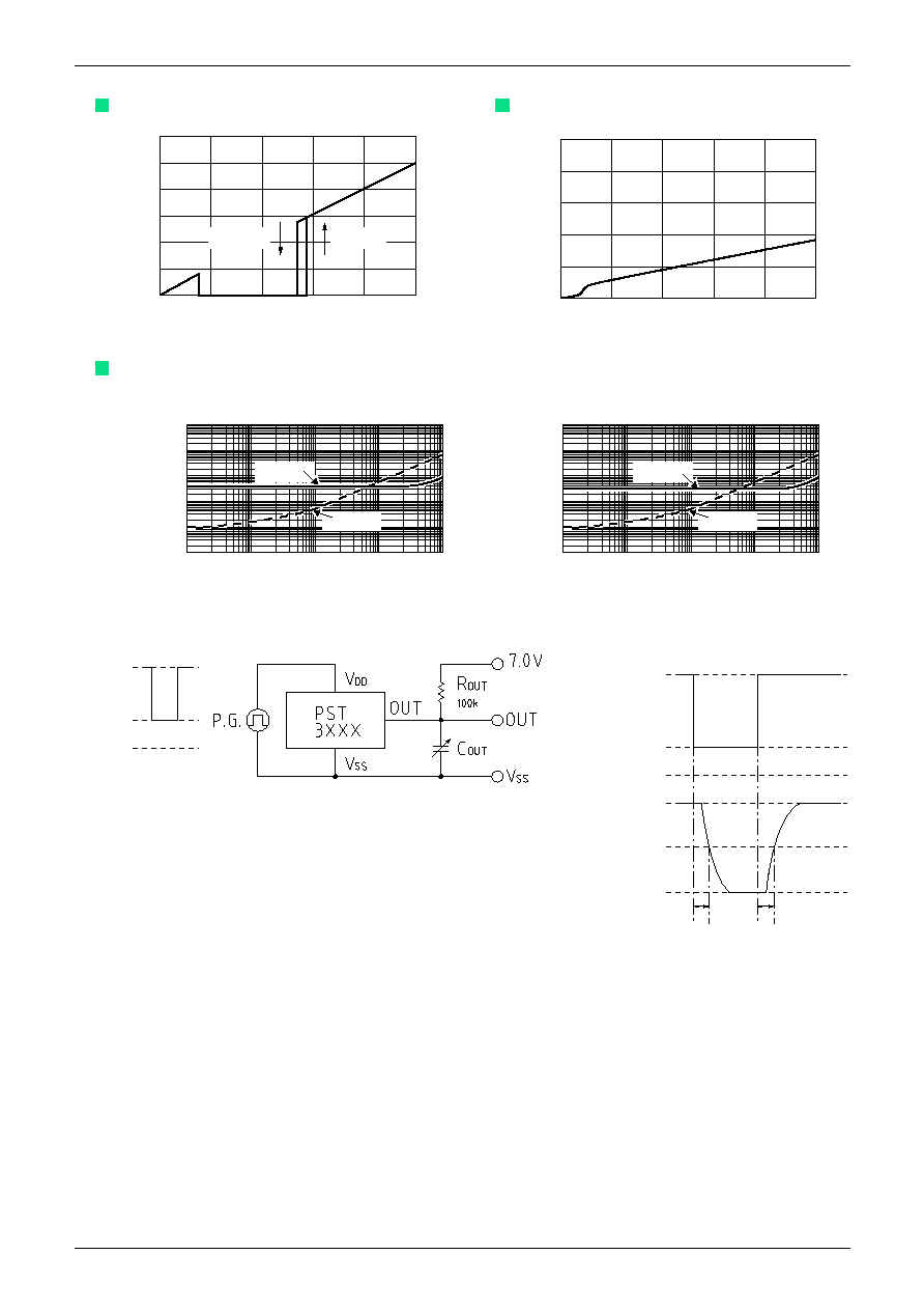
Output voltage power supply voltage
6
5
4
3
2
1
0
0
5
4
3
2
1
Detection
Release
Output voltage (V)
Power supply voltage (V)
Consumption current power supply voltage
1
0
0.2
0.4
0.6
0.8
0
10
8
6
4
2
Consumption current (
µ
A)
Power supply voltage (V)
Transfer delay time characteristics (N-ch open drain output products)
0.001
0.01
0.1
1
10
0.00001
0.1
0.01
0.001
0.0001
Response time (mS)
Output capacitance (
µ
F)
100
tPHL
tPLH
0.001
0.01
0.1
1
10
0.00001
0.1
0.01
0.001
0.0001
Response time (mS)
Output capacitance (
µ
F)
100
tPHL
tPLH
PST3428 response characteristics
PST3446 response characteristics
VS+2.0V
Input
voltage
Output
voltage
1.2V
7.0V
3.5V
V
SS
V
SS
tPHL
tPLH
VS+2.0V
1.2V
V
SS
Transfer delay time measurement circuit