 | –≠–ª–µ–∫—Ç—Ä–æ–Ω–Ω—ã–π –∫–æ–º–ø–æ–Ω–µ–Ω—Ç: 141540 | –°–∫–∞—á–∞—Ç—å:  PDF PDF  ZIP ZIP |

MC141540
1
MOTOROLA
Monitor On-Screen Display
CMOS
The MC141540 is a high performance HCMOS device designed to interface
with a microcontroller unit to allow colored symbols or characters to be
displayed on a color monitor. The on≠chip PLL allows both multi≠system
operation and self≠generation of system timing. It also minimizes the MCU's
burden through its built≠in 273 bytes display/control RAM. By storing a full
screen of data and control information, this device has a capability to carry out
`screen≠refresh' without MCU supervision.
Since there is no spacing between characters, special graphics≠oriented
characters can be generated by combining two or more character blocks.
Special functions such as character bordering or shadowing, multi≠level
windows, double height and double width, and programmable vertical length of
character can also be incorporated. Furthermore, neither massive information
update nor extremely high data transmission rate are expected for normal on≠
screen display operation, and serial protocols are implemented in lieu of any
parallel formats to achieve minimum pin count.
∑
Fixed Resolution: 320 (CGA) Dots per Line
∑
Fully Programmable Character Array of 10 Rows by 24 Columns
∑
273 Bytes Direct Mapping Display RAM Architecture
∑
Internal PLL Generates a Wide≠Ranged System Clock
∑
For High≠End Monitor Application, Maximum Horizontal Frequency is
100 kHz (32 MHz Dot Clock)
∑
Programmable Vertical Height of Character to Meet Multi≠Sync
Requirement
∑
Programmable Vertical and Horizontal Positioning for Display Center
∑
128 Characters and Graphic Symbols ROM
∑
10 x 16 Dot Matrix Character
∑
Character≠by≠Character Color Selection
∑
A Maximum of Four Selectable Colors per Row
∑
Double Character Height and Double Character Width
∑
Character Bordering or Shadowing
∑
Three Fully Programmable Background Windows with Overlapping
Capability
∑
Single Positive 5 V Supply
∑
MC141540P4 is a Replacement for XC141540P with Two Symbols Added
in ROM Addresses `5C' and `5E'
Order this document
by MC141540/D
MOTOROLA
SEMICONDUCTOR TECHNICAL DATA
PIN ASSIGNMENT
MC141540
P SUFFIX
PLASTIC DIP
CASE 648
ORDERING INFORMATION
MC141540P4
Plastic DIP
13
14
15
16
9
10
11
12
5
4
3
2
1
8
7
6
FBKG
B
G
R
VSS
VDD
VFLB
HTONE
VDD(A)
RP
VCO
SCL(SCK)
SDA(MOSI)
SS
HFLB
VSS(A)
©
Motorola, Inc. 1997
REV 1
2/97 TN97031200

MC141540
MOTOROLA
2
BLOCK DIAGRAM
ŒŒŒŒŒŒŒŒŒŒŒŒŒŒŒŒŒŒŒŒŒŒŒŒŒŒŒŒŒ
ŒŒŒŒŒŒŒŒŒŒŒŒŒŒŒŒŒŒŒŒŒŒŒŒŒŒŒŒŒ
ŒŒŒŒŒŒŒŒŒŒŒŒŒŒŒŒŒŒŒŒŒŒŒŒŒŒŒŒŒ
ŒŒŒŒŒŒŒŒŒŒŒŒŒŒŒŒŒŒŒŒŒŒŒŒŒŒŒŒŒ
ŒŒŒŒŒŒŒŒŒŒŒŒŒŒŒŒŒŒŒŒŒŒŒŒŒŒŒŒŒ
ŒŒŒŒŒŒŒŒŒŒŒŒŒŒŒŒŒŒŒŒŒŒŒŒŒŒŒŒŒ
ŒŒŒŒŒŒŒŒŒŒŒŒŒŒŒŒŒŒŒŒŒŒŒŒŒŒŒŒŒ
ŒŒŒŒŒŒŒŒŒŒŒŒŒŒŒŒŒŒŒŒŒŒŒŒŒŒŒŒŒ
ŒŒŒŒŒŒŒŒŒŒŒŒŒŒŒŒŒŒŒŒŒŒŒŒŒŒŒŒŒ
ŒŒŒŒŒŒŒŒŒŒŒŒŒŒŒŒŒŒŒŒŒŒŒŒŒŒŒŒŒ
ŒŒŒŒŒŒŒŒŒŒŒŒŒŒŒŒŒŒŒŒŒŒŒŒŒŒŒŒŒ
ŒŒŒŒŒŒŒŒŒŒŒŒŒŒŒŒŒŒŒŒŒŒŒŒŒŒŒŒŒ
ŒŒŒŒŒŒŒŒŒŒŒŒŒŒŒŒŒŒŒŒŒŒŒŒŒŒŒŒŒ
ŒŒŒŒŒŒŒŒŒŒŒŒŒŒŒŒŒŒŒŒŒŒŒŒŒŒŒŒŒ
ŒŒŒŒŒŒŒŒŒŒŒŒŒŒŒŒŒŒŒŒŒŒŒŒŒŒŒŒŒ
ŒŒŒŒŒŒŒŒŒŒŒŒŒŒŒŒŒŒŒŒŒŒŒŒŒŒŒŒŒ
ŒŒŒŒŒŒŒŒŒŒŒŒŒŒŒŒŒŒŒŒŒŒŒŒŒŒŒŒŒ
ŒŒŒŒŒŒŒŒŒŒŒŒŒŒŒŒŒŒŒŒŒŒŒŒŒŒŒŒŒ
ŒŒŒŒŒŒŒŒŒŒŒŒŒŒŒŒŒŒŒŒŒŒŒŒŒŒŒŒŒ
ŒŒŒŒŒŒŒŒŒŒŒŒŒŒŒŒŒŒŒŒŒŒŒŒŒŒŒŒŒ
ŒŒŒŒŒŒŒŒŒŒŒŒŒŒŒŒŒŒŒŒŒŒŒŒŒŒŒŒŒ
ŒŒŒŒŒŒŒŒŒŒŒŒŒŒŒŒŒŒŒŒŒŒŒŒŒŒŒŒŒ
ŒŒŒŒŒŒŒŒŒŒŒŒŒŒŒŒŒŒŒŒŒŒŒŒŒŒŒŒŒ
ŒŒŒŒŒŒŒŒŒŒŒŒŒŒŒŒŒŒŒŒŒŒŒŒŒŒŒŒŒ
ŒŒŒŒŒŒŒŒŒŒŒŒŒŒŒŒŒŒŒŒŒŒŒŒŒŒŒŒŒ
ŒŒŒŒŒŒŒŒŒŒŒŒŒŒŒŒŒŒŒŒŒŒŒŒŒŒŒŒŒ
ŒŒŒŒŒŒŒŒŒŒŒŒŒŒŒŒŒŒŒŒŒŒŒŒŒŒŒŒŒ
ŒŒŒŒŒŒŒŒŒŒŒŒŒŒŒŒŒŒŒŒŒŒŒŒŒŒŒŒŒ
ŒŒŒŒŒŒŒŒŒŒŒŒŒŒŒŒŒŒŒŒŒŒŒŒŒŒŒŒŒ
ŒŒŒŒŒŒŒŒŒŒŒŒŒŒŒŒŒŒŒŒŒŒŒŒŒŒŒŒŒ
ŒŒŒŒŒŒŒŒŒŒŒŒŒŒŒŒŒŒŒŒŒŒŒŒŒŒŒŒŒ
ŒŒŒŒŒŒŒŒŒŒŒŒŒŒŒŒŒŒŒŒŒŒŒŒŒŒŒŒŒ
ŒŒŒŒŒŒŒŒŒŒŒŒŒŒŒŒŒŒŒŒŒŒŒŒŒŒŒŒŒ
ŒŒŒŒŒŒŒŒŒŒŒŒŒŒŒŒŒŒŒŒŒŒŒŒŒŒŒŒŒ
ŒŒŒŒŒŒŒŒŒŒŒŒŒŒŒŒŒŒŒŒŒŒŒŒŒŒŒŒŒ
ŒŒŒŒŒŒŒŒŒŒŒŒŒŒŒŒŒŒŒŒŒŒŒŒŒŒŒŒŒ
ŒŒŒŒŒŒŒŒŒŒŒŒŒŒŒŒŒŒŒŒŒŒŒŒŒŒŒŒŒ
ŒŒŒŒŒŒŒŒŒŒŒŒŒŒŒŒŒŒŒŒŒŒŒŒŒŒŒŒŒ
ŒŒŒŒŒŒŒŒ
ŒŒŒŒŒŒŒŒ
ŒŒŒŒŒŒŒŒ
ŒŒŒŒŒŒŒŒ
ŒŒŒŒŒŒŒŒ
ŒŒŒŒŒ
ŒŒŒŒŒ
ŒŒŒŒŒ
ŒŒŒŒŒ
ŒŒŒŒŒ
ŒŒŒŒŒŒŒŒ
ŒŒŒŒŒŒŒŒ
ŒŒŒŒŒŒŒŒ
ŒŒŒŒŒŒŒŒ
ŒŒŒŒŒŒŒŒ
ŒŒŒŒŒŒŒŒ
ŒŒŒŒŒŒŒŒ
ŒŒŒŒŒŒŒŒ
ŒŒŒŒŒŒŒŒ
ŒŒŒŒŒŒŒŒ
ŒŒŒŒŒŒŒŒ
ŒŒŒŒŒŒŒŒ
ŒŒŒŒŒŒŒŒ
ŒŒŒŒŒŒŒŒ
ŒŒŒŒŒŒŒŒ
ŒŒŒŒŒŒŒŒ
ŒŒŒŒŒŒŒŒ
ŒŒŒŒŒŒŒŒ
ŒŒŒŒŒŒŒŒ
ŒŒŒŒŒŒŒŒ
ŒŒŒŒŒŒŒŒ
ŒŒŒŒŒŒŒŒ
ŒŒŒŒŒŒŒŒ
ŒŒŒŒŒŒŒŒ
ŒŒŒŒŒŒŒŒ
ŒŒŒŒŒŒŒŒ
ŒŒŒŒŒŒŒŒ
ŒŒŒŒŒŒŒŒ
ŒŒŒŒŒŒŒŒ
ŒŒŒŒŒŒŒŒ
ŒŒŒŒŒŒŒŒ
ŒŒŒŒŒŒŒŒ
ŒŒŒŒŒŒŒŒ
DATA RECEIVER
BUS ARBITRATION
VERTICAL
CONTROL
CIRCUIT
HORIZONTAL
CONTROL
BACKGROUND
GENERATOR
COLOR ENCODER
10≠BIT SHIFT
REGISTER
CHARACTER ROMS
ROW
BUFFER
LOGIC
WADDR
WCOLOR
CCOLORS
CHS
CWS
CRS
WCOLOR
AND CONTROL
CCOLORS
AND SELECT
WADDR
SC
HORD
5
CCLK
DHOR
LP
4
BLACKEDGE
MCLK
SDA(MOSI)
RP
VCO
SCL(SCK)
DATA
RA,CA,DA
RFG
ADDRC
Y
9
3
8
7
8
6
10
3
2
5
54
11
15
14
13
12
3
W
R
CHS
54
15
13
8
5
26
NROW
15
13
CWS
SHADOW
FBKG
HT
ONE
B
G
R
CHAR
CRADDR
OSD_EN
VERD
HORD
RDA
T
A
LUMINANCE
BSEN
SHADOW
BSEN
OSD_EN
5
CH
4
AND PLL
AND
CONTROL
8
VERD
4
Z
26
8
AND SELECT
6
10
9
1
16
VDD
VSS(A)
VDD(A)
MCLK
VSS
ŒŒŒŒŒŒŒŒ
ŒŒŒŒŒŒŒŒ
ŒŒŒŒŒŒŒŒ
ŒŒŒŒŒŒŒŒ
ŒŒŒŒŒŒŒŒ
MEMORY AND DATA
MANAGEMENT
SS
VFLB
HFLB

MC141540
3
MOTOROLA
ABSOLUTE MAXIMUM RATINGS
Voltage Referenced to VSS
Symbol
Characteristic
Value
Unit
VDD
Supply Voltage
≠ 0.3 to + 7.0
V
Vin
Input Voltage
VSS ≠ 0.3 to
VDD + 0.3
V
Id
Current Drain per Pin Excluding VDD
and VSS
25
mA
Ta
Operating Temperature Range
0 to 85
∞
C
Tstg
Storage Temperature Range
≠ 65 to + 150
∞
C
NOTE: Maximum Ratings are those values beyond which damage to the device may occur.
Functional operation should be restricted to the limits in the Electrical Characteris-
tics tables or Pin Description section.
AC ELECTRICAL CHARACTERISTICS
(VDD = VDD(A) = 5.0 V, VSS = VSS(A) = 0 V, TA = 25
∞
C, Voltage Referenced to VSS)
Symbol
Characteristic
Min
Typ
Max
Unit
tr
tf
Output Signal (R, G, B, FBKG and HTONE) Cload = 30 pF, see Figure 1
Rise Time
Fall Time
--
--
--
--
10
10
ns
ns
FHFLB
HFLB Input Frequency
--
--
100
kHz
DC CHARACTERISTICS
VDD = VDD(A) = 5.0 V
±
10%, VSS = VSS(A) = 0 V, TA = 25
∞
C, Voltage Referenced to VSS
Symbol
Characteristic
Min
Typ
Max
Unit
VOH
High Level Output Voltage
Iout = ≠ 5 mA
VDD ≠ 0.8
--
--
V
VOL
Low Level Output Voltage
Iout = 5 mA
--
--
VSS + 0.4
V
VIL
VIH
Digital Input Voltage (Not Including SDA and SCL)
Logic Low
Logic High
--
0.7 VDD
--
--
0.3 VDD
--
V
V
VIL
VIH
Input Voltage of Pin SDA and SCL in SPI Mode
Logic Low
Logic High
--
0.7 VDD
--
--
0.3 VDD
--
V
V
III
High≠Z Leakage Current (R, G, B and FBKG)
≠ 10
--
+ 10
µ
A
III
Input Current (Not Including RP, VCO, R, G, B, FBKG and HTONE)
≠ 10
--
+ 10
µ
A
IDD
Supply Current (No Load on Any Output)
--
9*
--
mA
* Not a guaranteed limit.
90%
10%
90%
10%
tf
tr
Figure 1. Switching Characteristics
This device contains circuitry to protect the
inputs against damage due to high static volt-
ages or electric fields; however, it is advised that
normal precautions be taken to avoid applica-
tions of any voltage higher than the maximum
rated voltages to this high impedance circuit.
For proper operation it is recommended that
Vin and Vout be constrained to the range VSS
(Vin or Vout)
VDD. Unused inputs must always
be tied to an appropriate logic voltage level (e.g.,
either VSS or VDD). Unused outputs must be left
open.

MC141540
MOTOROLA
4
PIN DESCRIPTIONS
VSS(A) (Pin 1)
This pin provides the signal ground to the PLL circuitry.
Analog ground for PLL operation is separated from digital
ground for optimal performance.
VCO (Pin 2)
Pin 2 is a control voltage input to regulate an internal oscil-
lator frequency. See the Application Diagram for the applica-
tion values used.
RP (Pin 3)
An external RC network is used to bias an internal VCO to
resonate at the specific dot frequency. The value of the resis-
tor for this pin should be adjusted in order to set the pin volt-
age to around half VDD. See the Application Diagram for the
application values used.
VDD(A) (Pin 4)
Pin 4 is a positive 5 V supply for PLL circuitry. Analog pow-
er for PLL is separated from digital power for optimal perfor-
mance.
HFLB (Pin 5)
This pin inputs a negative polarity horizontal synchronize
signal pulse to phase lock an internal system clock gener-
ated by the on≠chip VCO circuit.
SS (Pin 6)
This input pin is part of the SPI serial interface. An active
low signal generated by the master device enables this slave
device to accept data. This pin should be pulled high to termi-
nate the SPI communication.
SDA (MOSI) (Pin 7)
Data and control messages are being transmitted to this
chip from a host MCU via this wire, which is configured as a
uni≠directional data line. (Detailed description of these two
protocols will be discussed in the SPI section).
SCL (SCK) (Pin 8)
A separate synchronizing clock input from the transmitter
is required for either protocol. Data is read at the rising edge
of each clock signal.
VDD (Pin 9)
This is the power pin for the digital logic of the chip.
VFLB (Pin 10)
Similar to Pin 5, this pin inputs a negative polarity vertical
synchronize signal pulse.
HTONE (Pin 11)
This pin outputs a logic high during windowing except
when graphics or characters are being displayed. It is used
to lower the external R, G, and B amplifiers' gain to achieve a
transparent windowing effect.
FBKG (Pin 12)
This pin outputs a logic high while displaying characters or
windows when the FBKGC bit in the frame control register is
0, and output a logic high only while displaying characters
when the FBKGC bit is 1. It is defaulted to high≠impedance
state after power≠on, or when there is no output. An external
10 k
resistor pulled low is recommended to avoid level tog-
gling caused by hand effect when there is no output.
B,G,R (Pins 13,14,15)
MOSD color output is TTL level RGB to the host monitor.
These three signals are active high output pins that are in a
high≠impedance state when MOSD is disabled.
VSS (Pin 16)
This is the ground pin for the digital logic of the chip.
SYSTEM DESCRIPTION
MC141540 is a full≠screen memory architecture. Refresh
is performed by the built≠in circuitry after a screenful of dis-
play data has been loaded through the serial bus. Only
changes to the display data need to be input afterward.
Serial data, which includes screen mapping address, dis-
play information, and control messages, are transmitted via
the SPI bus. Figure 2 contains the SPI protocol operating
procedure.
Data is received from the serial port and stored by the
memory management circuit. Line data is stored in a row
buffer for display and refreshing. During this storing and re-
trieving cycle, bus arbitration logic patrols the internal traffic
to make sure that no crashes occur between the slower seri-
al bus receiver and the fast `screen≠refresh' circuitry. After
the full≠screen display data is received through one of the
serial communication interfaces, the link can be terminated if
a change of the display is not required.
The bottom half of the block diagram contains the hard-
ware functions for the entire system. It performs all the
MOSD functions such as programmable vertical length (from
16 lines to 63 lines), display clock generation (which is phase
locked to the incoming horizontal sync signal at Pin 5 HFLB),
bordering or shadowing, and multiple windowing.
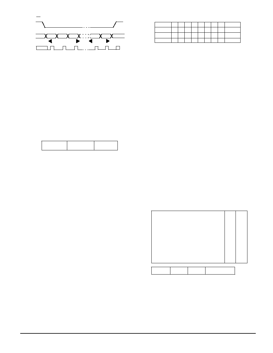
COMMUNICATION PROTOCOLS
Serial Peripheral Interface (SPI)
SPI is a three≠wire serial communication link that requires
separate clock (SCK) and data (MOSI) lines. In addition, an
SS slave select pin is controlled by the master transmitter to
initiate the receiver.
Operating Procedure
To initiate SPI transmission, the SS pin is pulled low by the
master device to enable MC141540 to accept data. The SS
input line must be a logic low prior to the occurrence of SCK,
and remain low until and after the last (eighth) SCK cycle. Af-
ter all data has been sent, the SS pin is then pulled high by
the master to terminate the transmission. No slave address
is needed for SPI. Hence, row and column address informa-
tion and display data can be sent immediately after the SPI is
initiated.
MC141540
5
MOTOROLA
……
……
MOSI
MSB
LSB
SCK
last byte
first byte
……
……
Figure 2. SPI Protocol
SS
DATA TRANSMISSION FORMATS
After the proper identification by the receiving device, a
data train of arbitrary length is transmitted from the master.
There are three transmission formats from (a) to (c) as stated
below. The data train in each sequence consists of row ad-
dress (R), column address (C), and display information (I), as
shown in Figure 3. In format (a), display information data
must be preceded with the corresponding row address and
column address. This format is particularly suitable for updat-
ing small amounts of data between different rows. However,
if the current information byte has the same row address as
the one before, format (b) is recommended.
ŒŒŒŒŒŒŒŒŒŒŒŒ
ŒŒŒŒŒŒŒŒŒŒŒŒ
row addr
col addr
info
Figure 3. Data Packet
For a full≠screen pattern change that requires a massive
information update, or during power≠up, most of the row and
column addresses of either (a) or (b) formats will be consec-
utive. Therefore, a more efficient data transmission format (c)
should be applied. This sends the RAM starting row and col-
umn addresses once only, and then treats all subsequent
data as display information. The row and column addresses
will be automatically incremented internally for each display
information data from the starting location. Because Col-
umns 24 through 29 are unused, it is recommended that
these locations are filled with dummy data while using format
(c) to transmit.
The data transmission formats are:
(a) R ≠ > C ≠ > I ≠ > R ≠ > C ≠ > I ≠ > . . . . . . . . .
(b) R ≠ > C ≠ > I ≠ > C ≠ > I ≠ > C ≠ > I. . . . . . .
(c) R ≠ > C ≠ > I ≠ > I ≠ > I ≠ > . . . . . . . . . . . . .
To differentiate the row and column addresses when trans-
ferring data from master, the MSB (most significant bit) is set,
as in Figure 4: `1' to represent row, and `0' for column ad-
dress. Furthermore, to distinguish the column address be-
tween formats (a), (b), and (c), the sixth bit of the column
address is set to `1' which represents format (c), and `0' for
format (a) or (b). However, there is some limitation on using
mixed formats during a single transmission. It is permissible
to change the format from (a) to (b), or from (a) to (c), or from
(b) to (a), but not from (c) back to (a) or (b).
ŒŒŒŒŒŒŒŒŒŒŒŒŒŒ
ŒŒŒŒŒŒŒŒŒŒŒŒŒŒ
ŒŒŒŒŒŒŒŒŒŒŒŒŒŒ
ŒŒŒŒŒŒŒŒŒŒŒŒŒŒ
ADDRESS
ROW
COLUMN
COLUMN
X: don't care
D: valid data
FORMAT
BIT
0
1
2
3
4
5
6
7
D
D
D
D
X
X
X
1
D
D
D
D
D
X
0
0
D
D
D
D
D
X
1
0
a, b
a, b, c
c
Figure 4. Row & Column Address Bit Patterns
MEMORY MANAGEMENT
Internal RAM is addressed with row and column (coln)
numbers in sequence. The spaces between Row 0 and Coln
0 to Row 9 and Coln 23 are called display registers, and each
contains a character ROM address corresponding to a dis-
play location on the monitor screen. Every data row is
associated with two control registers, which are located at
Coln 30 and 31 of their respective rows, to control the char-
acter display format of that row. In addition, three window
control registers for each of the three windows, together with
three frame control registers, occupy the first 13 columns of
Row 10.
The user should handle the internal RAM address location
with care, especially those rows with double length alphanu-
meric symbols. For example, if Row n is destined to be
double height on the memory map, the data displayed on
screen Rows n and n+1 will be represented by the data con-
tained in the memory address of Row n only. The data of the
next Row n+1 on the memory map will appear on the screen
as n+2 and n+3 row space, and so on. Hence, it is not neces-
sary to load a row of blank data to compensate for the double
row. The user should minimize excessive rows of data in
memory in order to avoid overrunning the limited amount of
row space on the screen.
For rows with double width alphanumeric symbols, only
the data contained in the even numbered columns of the
memory map are shown. Odd numbered columns are
treated in the same manner as double height rows.
ŒŒŒŒŒŒŒŒŒŒŒŒŒŒŒ
ŒŒŒŒŒŒŒŒŒŒŒŒŒŒŒ
ŒŒŒŒŒŒŒŒŒŒŒŒŒŒŒ
ŒŒŒŒŒŒŒŒŒŒŒŒŒŒŒ
ŒŒŒŒŒŒŒŒŒŒŒŒŒŒŒ
ŒŒŒŒŒŒŒŒŒŒŒŒŒŒŒ
ŒŒŒŒŒŒŒŒŒŒŒŒŒŒŒ
ŒŒŒŒŒŒŒŒŒŒŒŒŒŒŒ
ŒŒŒŒŒŒŒŒŒŒŒŒŒŒŒ
DISPLAY REGISTERS
COLUMN
29 30 31
0
0
9
ROW
ROW CONTROL
REGISTERS
WINDOW 1 WINDOW 2
FRAME CRTL REG
WINDOW 3
10
0
2 3
5 6
8 9
12
23 24...
WINDOW AND FRAME CONTROL REGISTERS
Figure 5. Memory Map
RESER
VED SP
ACE