 | –≠–ª–µ–∫—Ç—Ä–æ–Ω–Ω—ã–π –∫–æ–º–ø–æ–Ω–µ–Ω—Ç: 1N5821 | –°–∫–∞—á–∞—Ç—å:  PDF PDF  ZIP ZIP |

1
Rectifier Device Data
Designer's
TM
Data Sheet
Axial Lead Rectifiers
. . . employing the Schottky Barrier principle in a large area metal≠to≠silicon
power diode. State≠of≠the≠art geometry features chrome barrier metal,
epitaxial construction with oxide passivation and metal overlap contact. Ideally
suited for use as rectifiers in low≠voltage, high≠frequency inverters, free
wheeling diodes, and polarity protection diodes.
∑
Extremely Low vF
∑
Low Power Loss/High Efficiency
∑
Low Stored Charge, Majority Carrier Conduction
Mechanical Characteristics:
∑
Case: Epoxy, Molded
∑
Weight: 1.1 gram (approximately)
∑
Finish: All External Surfaces Corrosion Resistant and Terminal Leads are
Readily Solderable
∑
Lead and Mounting Surface Temperature for Soldering Purposes: 220
∞
C
Max. for 10 Seconds, 1/16
from case
∑
Shipped in plastic bags, 5,000 per bag
∑
Available Tape and Reeled, 1500 per reel, by adding a "RL'' suffix to the
part number
∑
Polarity: Cathode indicated by Polarity Band
∑
Marking: 1N5820, 1N5821, 1N5822
MAXIMUM RATINGS
Rating
Symbol
1N5820
1N5821
1N5822
Unit
Peak Repetitive Reverse Voltage
Working Peak Reverse Voltage
DC Blocking Voltage
VRRM
VRWM
VR
20
30
40
V
Non≠Repetitive Peak Reverse Voltage
VRSM
24
36
48
V
RMS Reverse Voltage
VR(RMS)
14
21
28
V
Average Rectified Forward Current (2)
VR(equiv)
v
0.2 VR(dc), TL = 95
∞
C
(R
JA = 28
∞
C/W, P.C. Board Mounting, see Note 2)
IO
3.0
A
Ambient Temperature
Rated VR(dc), PF(AV) = 0
R
JA = 28
∞
C/W
TA
90
85
80
∞
C
Non≠Repetitive Peak Surge Current
(Surge applied at rated load conditions, half wave, single phase
60 Hz, TL = 75
∞
C)
IFSM
80 (for one cycle)
A
Operating and Storage Junction Temperature Range
(Reverse Voltage applied)
TJ, Tstg
*
65 to +125
∞
C
Peak Operating Junction Temperature (Forward Current applied)
TJ(pk)
150
∞
C
*THERMAL CHARACTERISTICS
(Note 2)
Characteristic
Symbol
Max
Unit
Thermal Resistance, Junction to Ambient
R
JA
28
∞
C/W
(1) Pulse Test: Pulse Width = 300
µ
s, Duty Cycle = 2.0%.
(2) Lead Temperature reference is cathode lead 1/32
from case.
* Indicates JEDEC Registered Data for 1N5820≠22.
Designer's Data for "Worst Case" Conditions -- The Designer's Data Sheet permits the design of most circuits entirely from the information presented. SOA Limit
curves -- representing boundaries on device characteristics -- are given to facilitate "worst case" design.
Preferred devices are Motorola recommended choices for future use and best overall value.
©
Motorola, Inc. 1996
Order this document
by 1N5820/D
MOTOROLA
SEMICONDUCTOR TECHNICAL DATA
1N5820
1N5821
1N5822
SCHOTTKY BARRIER
RECTIFIERS
3.0 AMPERES
20, 30, 40 VOLTS
CASE 267≠03
PLASTIC
1N5820 and 1N5822 are
Motorola Preferred Devices
Rev 2
1N5820 1N5821 1N5822
2
Rectifier Device Data
*ELECTRICAL CHARACTERISTICS
(TL = 25
∞
C unless otherwise noted) (2)
Characteristic
Symbol
1N5820
1N5821
1N5822
Unit
Maximum Instantaneous Forward Voltage (1)
(iF = 1.0 Amp)
(iF = 3.0 Amp)
(iF = 9.4 Amp)
VF
0.370
0.475
0.850
0.380
0.500
0.900
0.390
0.525
0.950
V
Maximum Instantaneous Reverse Current @ Rated dc Voltage (1)
TL = 25
∞
C
TL = 100
∞
C
iR
2.0
20
2.0
20
2.0
20
mA
(1) Pulse Test: Pulse Width = 300
µ
s, Duty Cycle = 2.0%.
(2) Lead Temperature reference is cathode lead 1/32
from case.
* Indicates JEDEC Registered Data for 1N5820≠22.
NOTE 1 -- DETERMINING MAXIMUM RATINGS
Reverse power dissipation and the possibility of thermal runaway
must be considered when operating this rectifier at reverse voltages
above 0.1 VRWM. Proper derating may be accomplished by use of
equation (1).
TA(max) = TJ(max)
*
R
JAPF(AV)
*
R
JAPR(AV)
(1)
where TA(max) = Maximum allowable ambient temperature
TJ(max) = Maximum allowable junction temperature
(125
∞
C or the temperature at which thermal
runaway occurs, whichever is lowest)
PF(AV) = Average forward power dissipation
PR(AV) = Average reverse power dissipation
R
JA = Junction≠to≠ambient thermal resistance
Figures 1, 2, and 3 permit easier use of equation (1) by taking
reverse power dissipation and thermal runaway into consideration.
The figures solve for a reference temperature as determined by
equation (2).
TR = TJ(max)
*
R
JAPR(AV)
(2)
Substituting equation (2) into equation (1) yields:
TA(max) = TR
*
R
JAPF(AV)
(3)
Inspection of equations (2) and (3) reveals that TR is the ambient
temperature at which thermal runaway occurs or where TJ = 125
∞
C,
when forward power is zero. The transition from one boundary condi-
tion to the other is evident on the curves of Figures 1, 2, and 3 as a
difference in the rate of change of the slope in the vicinity of 115
∞
C.
The data of Figures 1, 2, and 3 is based upon dc conditions. For use
in common rectifier circuits, Table 1 indicates suggested factors for
an equivalent dc voltage to use for conservative design, that is:
VR(equiv) = V(FM)
F
(4)
The factor F is derived by considering the properties of the various
rectifier circuits and the reverse characteristics of Schottky diodes.
EXAMPLE: Find TA(max) for 1N5821 operated in a 12≠volt dc sup-
ply using a bridge circuit with capacitive filter such that IDC = 2.0 A
(IF(AV) = 1.0 A), I(FM)/I(AV) = 10, Input Voltage = 10 V(rms), R
JA =
40
∞
C/W.
Step 1. Find VR(equiv). Read F = 0.65 from Table 1,
N
VR(equiv) = (1.41) (10) (0.65) = 9.2 V.
Step 2. Find TR from Figure 2. Read TR = 108
∞
C
@ VR = 9.2 V and R
JA = 40
∞
C/W.
Step 3. Find PF(AV) from Figure 6. **Read PF(AV) = 0.85 W
@
I(FM)
I(AV)
+
10 and IF(AV)
+
1.0 A.
Step 4. Find TA(max) from equation (3).
TA(max) = 108
*
(0.85) (40) = 74
∞
C.
**Values given are for the 1N5821. Power is slightly lower for the
1N5820 because of its lower forward voltage, and higher for the
1N5822. Variations will be similar for the MBR≠prefix devices, using
PF(AV) from Figure 7.
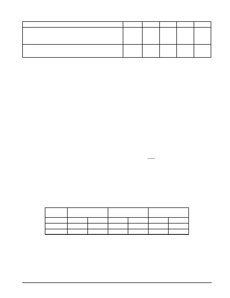
Table 1. Values for Factor F
Circuit
Half Wave
Full Wave, Bridge
Full Wave,
Center Tapped*
Load
Resistive
Capacitive*
Resistive
Capacitive
Resistive
Capacitive
Sine Wave
0.5
1.3
0.5
0.65
1.0
1.3
Square Wave
0.75
1.5
0.75
0.75
1.5
1.5
*Note that VR(PK)
[
2.0 Vin(PK). Use line to center tap voltage for Vin.

1N5820 1N5821 1N5822
3
Rectifier Device Data
Figure 1. Maximum Reference Temperature
1N5820
Figure 2. Maximum Reference Temperature
1N5821
Figure 3. Maximum Reference Temperature
1N5822
Figure 4. Steady≠State Thermal Resistance
15
2.0
VR, REVERSE VOLTAGE (VOLTS)
115
125
105
30
4.0
VR, REVERSE VOLTAGE (VOLTS)
125
115
105
95
85
75
L, LEAD LENGTH (INCHES)
1/8
0
25
20
15
10
5.0
0
2/8
40
T
R
, REFERENCE
TEMPERA
TURE ( C)
T
R
JL
, THERMAL
RESIST
ANCE
95
85
75
5.0
3.0
4.0
7.0
10
20
∞
5.0
7.0
10
15
20
3/8
4/8
5/8
6/8
7/8
1.0
40
35
30
q
JUNCTION≠T
O≠LEAD ( C/W)
∞
BOTH LEADS TO HEAT SINK,
EQUAL LENGTH
MAXIMUM
TYPICAL
, REFERENCE
TEMPERA
TURE ( C)
R
∞
R
q
JA (
∞
C/W) = 70
50
40
28
20
15
10
8.0
15
VR, REVERSE VOLTAGE (VOLTS)
115
105
T
R
, REFERENCE
TEMPERA
TURE ( C)
95
85
75
5.0
3.0
4.0
7.0
10
20
∞
R
q
JA (
∞
C/W) = 70
50
40
28
20
15
10
8.0
125
30
R
q
JA (
∞
C/W) = 70
50
40
28
20
15
10
8.0

1N5820 1N5821 1N5822
4
Rectifier Device Data
r(t), TRANSIENT
THERMAL
RESIST
ANCE
(NORMALIZED)
0.2
0.5
1.0
2.0
5.0
10
20
50
100
200
500
1.0 k
2.0 k
5.0 k
10 k
0.05
0.03
0.02
0.01
0.1
t, TIME (ms)
0.5
0.3
0.2
1.0
LEAD LENGTH = 1/4
Ppk
Ppk
tp
t1
TIME
DUTY CYCLE = tp/t1
PEAK POWER, Ppk, is peak of an
equivalent square power pulse.
TJL = Ppk
∑
R
JL [D + (1 ≠ D)
∑
r(t1 + tp) + r(tp) ≠ r(t1)] where:
TJL = the increase in junction temperature above the lead temperature.
r(t) = normalized value of transient thermal resistance at time, t, i.e.:
r(t1 + tp) = normalized value of transient thermal resistance at time
t1 + tp, etc.
Figure 5. Thermal Response
20 k
The temperature of the lead should be measured using a ther-
mocouple placed on the lead as close as possible to the tie point.
The thermal mass connected to the tie point is normally large
enough so that it will not significantly respond to heat surges
generated in the diode as a result of pulsed operation once
steady≠state conditions are achieved. Using the measured val-
ue of TL, the junction temperature may be determined by:
TJ = TL +
D
TJL
3.0
0.1
IF(AV), AVERAGE FORWARD CURRENT (AMP)
10
7.0
5.0
0.7
0.5
0.1
5.0
P
0.2
0.3
0.5
2.0
,
A
VERAGE POWER DISSIP
A
TION
(W
A
TTS)
F(A
V)
3.0
2.0
1.0
0.3
0.2
0.7 1.0
7.0
10
Figure 6. Forward Power Dissipation 1N5820≠22
dc
SQUARE WAVE
TJ
125
∞
C
SINE WAVE
I
(FM)
I
(AV)
+ p
(Resistive Load)
Capacitive
Loads
5.0
10
20
TA(A)
TA(K)
TL(A)
TC(A)
TJ
TC(K)
TL(K)
PD
R
S(A)
R
L(A)
R
J(A)
R
J(K)
R
L(K)
R
S(K)
NOTE 3 -- APPROXIMATE THERMAL CIRCUIT MODEL
Use of the above model permits junction to lead thermal resis-
tance for any mounting configuration to be found. For a given total
lead length, lowest values occur when one side of the rectifier is
brought as close as possible to the heat sink. Terms in the model
signify:
TA = Ambient Temperature
TC = Case Temperature
TL = Lead Temperature
TJ = Junction Temperature
R
S = Thermal Resistance, Heat Sink to Ambient
R
L = Thermal Resistance, Lead to Heat Sink
R
J = Thermal Resistance, Junction to Case
PD = Total Power Dissipation = PF + PR
PF = Forward Power Dissipation
PR = Reverse Power Dissipation
(Subscripts (A) and (K) refer to anode and cathode sides, respec-
tively.) Values for thermal resistance components are:
R
L = 42
∞
C/W/in typically and 48
∞
C/W/in maximum
R
J = 10
∞
C/W typically and 16
∞
C/W maximum
The maximum lead temperature may be found as follows:
TL = TJ(max)
*
n
TJL
where
n
TJL
[
R
JL ∑ PD
TYPICAL VALUES FOR R
JA IN STILL AIR
Data shown for thermal resistance junction≠to≠ambient (R
JA)
for the mountings shown is to be used as typical guideline values
for preliminary engineering, or in case the tie point temperature
cannot be measured.
1
2
3
Mounting
Method
Lead Length, L (in)
1/8
1/4
1/2
3/4
R
JA
50
51
53
55
∞
C/W
∞
C/W
∞
C/W
58
59
61
63
28
NOTE 2 -- MOUNTING DATA
Mounting Method 1
P.C. Board where available
copper surface is small.
Mounting Method 3
P.C. Board with
2≠1/2
x 2≠1/2
copper surface.
BOARD GROUND
PLANE
VECTOR PUSH≠IN
TERMINALS T≠28
Mounting Method 2
…………………
…………………
L
L
……………………
L
L
……
……
……
……
……
L = 1/2

1N5820 1N5821 1N5822
5
Rectifier Device Data
75
∞
C
25
∞
C
100
∞
C
TJ = 125
∞
C
NOTE 4 -- HIGH FREQUENCY OPERATION
Since current flow in a Schottky rectifier is the result of majority
carrier conduction, it is not subject to junction diode forward and
reverse recovery transients due to minority carrier injection and
stored charge. Satisfactory circuit analysis work may be performed
by using a model consisting of an ideal diode in parallel with a
variable capacitance. (See Figure 11.)
Figure 7. Typical Forward Voltage
Figure 8. Maximum Non≠Repetitive Surge
Current
Figure 9. Typical Reverse Current
1.2
vF, INSTANTANEOUS FORWARD VOLTAGE (VOLTS)
50
5.0
NUMBER OF CYCLES
5.0
100
1.0
10
VR, REVERSE VOLTAGE (VOLTS)
8.0
0
50
0.2
0.01
16
i F
, INST
ANT
ANEOUS
FOR
W
ARD
CURRENT
(AMP)
I
0.5
0.4
0
0.2
0.6
0.8
7.0 10
2.0
3.0
100
24
32
40
0.05
1.4
100
20
0.1
, PEAK HALF≠W
A
VE
CURRENT
(AMP)
FSM
70
50
30
20
TJ = 100
∞
C
25
∞
C
1.0
0.3
0.2
0.1
0.07
0.7
1.0
2.0
3.0
7.0
10
20
30
VR, REVERSE VOLTAGE (VOLTS)
1.0
0.5
200
70
2.0
3.0
5.0
10
500
300
100
C, CAP
ACIT
ANCE
(pF)
0.7
7.0
20
30
1N5820
1N5821
1N5822
TJ = 25
∞
C
f = 1.0 MHz
20
30
50
70
TL = 75
∞
C
f = 60 Hz
SURGE APPLIED AT RATED LOAD CONDITIONS
Figure 10. Typical Capacitance
I
,
REVERSE CURRENT
(mA)
R
0.02
0.05
10
1.0
0.5
5.0
2.0
4.0
12
20
28
36
1N5820
1N5821
1N5822
1 CYCLE
1.1
0.3
0.1
0.5
0.7
1.3
0.9