 | –≠–ª–µ–∫—Ç—Ä–æ–Ω–Ω—ã–π –∫–æ–º–ø–æ–Ω–µ–Ω—Ç: 2N5551 | –°–∫–∞—á–∞—Ç—å:  PDF PDF  ZIP ZIP |

1
Motorola Small≠Signal Transistors, FETs and Diodes Device Data
Amplifier Transistors
NPN Silicon
MAXIMUM RATINGS
Rating
Symbol
2N5550
2N5551
Unit
Collector ≠ Emitter Voltage
VCEO
140
160
Vdc
Collector ≠ Base Voltage
VCBO
160
180
Vdc
Emitter ≠ Base Voltage
VEBO
6.0
Vdc
Collector Current -- Continuous
IC
600
mAdc
Total Device Dissipation @ TA = 25
∞
C
Derate above 25
∞
C
PD
625
5.0
mW
mW/
∞
C
Total Device Dissipation @ TC = 25
∞
C
Derate above 25
∞
C
PD
1.5
12
Watts
mW/
∞
C
Operating and Storage Junction
Temperature Range
TJ, Tstg
≠ 55 to +150
∞
C
THERMAL CHARACTERISTICS
Characteristic
Symbol
Max
Unit
Thermal Resistance, Junction to Ambient
R
q
JA
200
∞
C/W
Thermal Resistance, Junction to Case
R
q
JC
83.3
∞
C/W
ELECTRICAL CHARACTERISTICS
(TA = 25
∞
C unless otherwise noted)
Characteristic
Symbol
Min
Max
Unit
OFF CHARACTERISTICS
Collector ≠ Emitter Breakdown Voltage(1)
(IC = 1.0 mAdc, IB = 0)
2N5550
2N5551
V(BR)CEO
140
160
--
--
Vdc
Collector ≠ Base Breakdown Voltage
(IC = 100
µ
Adc, IE = 0 )
2N5550
2N5551
V(BR)CBO
160
180
--
--
Vdc
Emitter ≠ Base Breakdown Voltage
(IE = 10
µ
Adc, IC = 0)
V(BR)EBO
6.0
--
Vdc
Collector Cutoff Current
(VCB = 100 Vdc, IE = 0)
2N5550
(VCB = 120 Vdc, IE = 0)
2N5551
(VCB = 100 Vdc, IE = 0, TA = 100
∞
C)
2N5550
(VCB = 120 Vdc, IE = 0, TA = 100
∞
C)
2N5551
ICBO
--
--
--
--
100
50
100
50
nAdc
µ
Adc
Emitter Cutoff Current
(VEB = 4.0 Vdc, IC = 0)
IEBO
--
50
nAdc
1. Pulse Test: Pulse Width = 300
m
s, Duty Cycle = 2.0%.
Preferred devices are Motorola recommended choices for future use and best overall value.
Order this document
by 2N5550/D
MOTOROLA
SEMICONDUCTOR TECHNICAL DATA
2N5550
2N5551
*Motorola Preferred Device
*
CASE 29≠04, STYLE 1
TO≠92 (TO≠226AA)
1
2
3
©
Motorola, Inc. 1996
COLLECTOR
3
2
BASE
1
EMITTER

2N5550 2N5551
2
Motorola Small≠Signal Transistors, FETs and Diodes Device Data
ELECTRICAL CHARACTERISTICS
(TA = 25
∞
C unless otherwise noted) (Continued)
Characteristic
Symbol
Min
Max
Unit
ON CHARACTERISTICS(1)
DC Current Gain
(IC = 1.0 mAdc, VCE = 5.0 Vdc)
2N5550
2N5551
(IC = 10 mAdc, VCE = 5.0 Vdc)
2N5550
2N5551
(IC = 50 mAdc, VCE = 5.0 Vdc)
2N5550
2N5551
hFE
60
80
60
80
20
30
--
--
250
250
--
--
--
Collector ≠ Emitter Saturation Voltage
(IC = 10 mAdc, IB = 1.0 mAdc)
Both Types
(IC = 50 mAdc, IB = 5.0 mAdc)
2N5550
2N5551
VCE(sat)
--
--
--
0.15
0.25
0.20
Vdc
Base ≠ Emitter Saturation Voltage
(IC = 10 mAdc, IB = 1.0 mAdc)
Both Types
(IC = 50 mAdc, IB = 5.0 mAdc)
2N5550
2N5551
VBE(sat)
--
--
--
1.0
1.2
1.0
Vdc
SMALL≠ SIGNAL CHARACTERISTICS
Current ≠ Gain -- Bandwidth Product
(IC = 10 mAdc, VCE = 10 Vdc, f = 100 MHz)
fT
100
300
MHz
Output Capacitance
(VCB = 10 Vdc, IE = 0, f = 1.0 MHz)
Cobo
--
6.0
pF
Input Capacitance
(VEB = 0.5 Vdc, IC = 0, f = 1.0 MHz)
2N5550
2N5551
Cibo
--
--
30
20
pF
Small≠Signal Current Gain
(IC = 1.0 mAdc, VCE = 10 Vdc, f = 1.0 kHz)
hfe
50
200
--
Noise Figure
(IC = 250
µ
Adc, VCE = 5.0 Vdc, RS = 1.0 k
,
2N5550
f = 1.0 kHz)
2N5551
NF
--
--
10
8.0
dB
1. Pulse Test: Pulse Width = 300
m
s, Duty Cycle = 2.0%.

2N5550 2N5551
3
Motorola Small≠Signal Transistors, FETs and Diodes Device Data
Figure 1. DC Current Gain
IC, COLLECTOR CURRENT (mA)
500
h , DC CURRENT
GAIN
FE
TJ = 125
∞
C
≠ 55
∞
C
25
∞
C
5.0
10
0.1
0.2
0.3
0.5
0.7
1.0
2.0
3.0
5.0
7.0
10
20
30
50
70
100
200
30
20
300
100
50
7.0
VCE = 1.0 V
VCE = 5.0 V
Figure 2. Collector Saturation Region
IB, BASE CURRENT (mA)
1.0
IC = 1.0 mA
0
0.3
0.005
0.01
0.2
0.5
1.0
2.0
20
50
0.8
0.5
0.4
0.9
0.7
0.6
0.2
0.02
0.05
0.1
10
V
CE
, COLLECT
OR≠EMITTER VOL
T
AGE (VOL
TS)
0.1
10 mA
30 mA
100 mA
5.0

2N5550 2N5551
4
Motorola Small≠Signal Transistors, FETs and Diodes Device Data
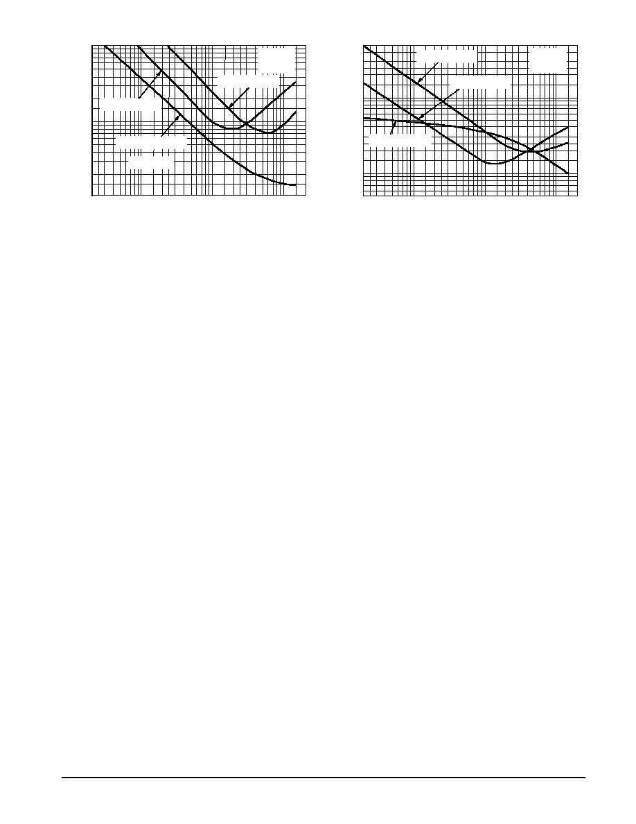
Figure 3. Collector Cut≠Off Region
IC, COLLECTOR CURRENT (mA)
1.0
IC, COLLECTOR CURRENT (mA)
V
, VOL
T
AGE (VOL
TS)
1.0
2.0
5.0
10
20
50
2.5
100
TJ = 25
∞
C
VBE(sat) @ IC/IB = 10
VCE(sat) @ IC/IB = 10
q
VC for VCE(sat)
q
VB for VBE(sat)
0.1
0.2
0.5
Figure 4. "On" Voltages
VBE, BASE≠EMITTER VOLTAGE (VOLTS)
101
10≠5
Figure 5. Temperature Coefficients
TJ = ≠ 55
∞
C to +135
∞
C
0.4
0.3
0.1
0.8
0.6
0.4
0.2
0
100
10≠1
10≠2
10≠3
10≠4
0.2
0
0.1
0.2
0.4
0.3
0.6
0.5
VCE = 30 V
TJ = 125
∞
C
75
∞
C
25
∞
C
IC = ICES
, COLLECT
OR CURRENT
(
A)
µ
I C
V
,
TEMPERA
TURE COEFFICIENT
(mV/
C)
∞
3.0
30
2.0
1.5
1.0
0.5
0
≠ 0.5
≠ 1.0
≠ 1.5
≠ 2.0
≠ 2.5
C, CAP
ACIT
ANCE (pF)
Figure 6. Switching Time Test Circuit
VR, REVERSE VOLTAGE (VOLTS)
100
1.0
0.2
0.5
1.0
2.0
5.0
10
20
Cibo
70
50
30
20
10
7.0
5.0
3.0
2.0
0.3
0.7
3.0
7.0
Cobo
Figure 7. Capacitances
REVERSE
FORWARD
0.3
1.0
2.0
5.0
10
20
50
100
0.1
0.2
0.5
3.0
30
0.3
10.2 V
Vin
10
µ
s
INPUT PULSE
VBB
≠ 8.8 V
100
RB
5.1 k
0.25
µ
F
Vin
100
1N914
Vout
RC
VCC
30 V
3.0 k
tr, tf
10 ns
DUTY CYCLE = 1.0%
Values Shown are for IC @ 10 mA
TJ = 25
∞
C
2N5550 2N5551
5
Motorola Small≠Signal Transistors, FETs and Diodes Device Data
Figure 8. Turn≠On Time
IC, COLLECTOR CURRENT (mA)
1000
Figure 9. Turn≠Off Time
IC, COLLECTOR CURRENT (mA)
0.3
1.0
10
20 30
50
5000
0.5
0.2
t,
TIME (ns)
t,
TIME (ns)
10
20
30
50
100
200
300
500
2.0
100
200
IC/IB = 10
TJ = 25
∞
C
tr @ VCC = 120 V
50
100
200
300
500
3.0 5.0
tr @ VCC = 30 V
td @ VEB(off) = 1.0 V
VCC = 120 V
3000
2000
1000
0.3
1.0
10
20 30 50
0.5
0.2
2.0
100
200
3.0 5.0
IC/IB = 10
TJ = 25
∞
C
tf @ VCC = 120 V
tf @ VCC = 30 V
ts @ VCC = 120 V