 | –≠–ª–µ–∫—Ç—Ä–æ–Ω–Ω—ã–π –∫–æ–º–ø–æ–Ω–µ–Ω—Ç: 4N33 | –°–∫–∞—á–∞—Ç—å:  PDF PDF  ZIP ZIP |

1
Motorola Optoelectronics Device Data
6-Pin DIP Optoisolators
Darlington Output
The 4N29/A, 4N30, 4N31, 4N32
(1)
and 4N33
(1)
devices consist of a gallium
arsenide infrared emitting diode optically coupled to a monolithic silicon
photodarlington detector.
This series is designed for use in applications requiring high collector output
currents at lower input currents.
∑
Higher Sensitivity to Low Input Drive Current
∑
Meets or Exceeds All JEDEC Registered Specifications
∑
To order devices that are tested and marked per VDE 0884 requirements, the
suffix "V" must be included at end of part number. VDE 0884 is a test option.
Applications
∑
Low Power Logic Circuits
∑
Interfacing and coupling systems of different potentials and impedances
∑
Telecommunications Equipment
∑
Portable Electronics
∑
Solid State Relays
MAXIMUM RATINGS
(TA = 25
∞
C unless otherwise noted)
Rating
Symbol
Value
Unit
INPUT LED
Reverse Voltage
VR
3
Volts
Forward Current -- Continuous
IF
60
mA
LED Power Dissipation @ TA = 25
∞
C
Derate above 25
∞
C
PD
120
1.41
mW
mW/
∞
C
OUTPUT DETECTOR
Collector≠Emitter Voltage
VCEO
30
Volts
Emitter≠Collector Voltage
VECO
5
Volts
Collector≠Base Voltage
VCBO
30
Volts
Collector Current -- Continuous
IC
150
mA
Detector Power Dissipation @ TA = 25
∞
C
Derate above 25
∞
C
PD
150
1.76
mW
mW/
∞
C
TOTAL DEVICE
Isolation Surge Voltage(2)
(Peak ac Voltage, 60 Hz, 1 sec Duration)
VISO
7500
Vac(pk)
Total Device Power Dissipation @ TA = 25
∞
C
Derate above 25
∞
C
PD
250
2.94
mW
mW/
∞
C
Ambient Operating Temperature Range(3)
TA
≠ 55 to +100
∞
C
Storage Temperature Range(3)
Tstg
≠ 55 to +150
∞
C
Soldering Temperature (10 sec, 1/16
from case)
TL
260
∞
C
1. Difference in 4N32 and 4N33 is JEDEC Registration for VISO only. All Motorola 6≠Pin devices
exceed JEDEC specification and are 7500 Vac(pk). The same applies for 4N29 and 4N30.
2. Isolation surge voltage is an internal device dielectric breakdown rating. For this test, Pins 1 and
2 are common, and Pins 4, 5 and 6 are common.
3. Refer to Quality and Reliability Section in Opto Data Book for information on test conditions.
Preferred devices are Motorola recommended choices for future use and best overall value.
GlobalOptoisolator is a trademark of Motorola, Inc.
Order this document
by 4N29/D
MOTOROLA
SEMICONDUCTOR TECHNICAL DATA
GlobalOptoisolator
TM
4N29
4N29A
4N30
4N31
4N32
4N33
*Motorola Preferred Devices
SCHEMATIC
[CTR = 100% Min]
*
[CTR = 500% Min]
STANDARD THRU HOLE
CASE 730A≠04
STYLE 1 PLASTIC
*
*
[CTR = 50% Min]
PIN 1. LED ANODE
2. LED CATHODE
3. N.C.
4. EMITTER
5. COLLECTOR
6. BASE
1
2
3
6
5
4
6
1
©
Motorola, Inc. 1995
REV 4
4N29 4N29A 4N30 4N31 4N32 4N33
2
Motorola Optoelectronics Device Data
ELECTRICAL CHARACTERISTICS
(TA = 25
∞
C unless otherwise noted)(1)
Characteristic
Symbol
Min
Typ(1)
Max
Unit
INPUT LED
*Reverse Leakage Current (VR = 3 V, RL = 1 M ohms)
IR
--
0.05
100
µ
A
*Forward Voltage (IF = 10 mA)
VF
--
1.34
1.5
Volts
Capacitance (VR = 0 V, f = 1 MHz)
C
--
1.8
--
pF
OUTPUT DETECTOR (TA = 25
∞
C and IF = 0, unless otherwise noted)
*Collector≠Emitter Dark Current
(VCE = 10 V, Base Open)
I
CEO
--
--
100
nA
*Collector≠Base Breakdown Voltage
(IC = 100
µ
A, IE = 0)
V(BR)CBO
30
--
--
Volts
*Collector≠Emitter Breakdown Voltage
(IC = 100
µ
A, IB = 0)
V(BR)CEO
30
--
--
Volts
*Emitter≠Collector Breakdown Voltage
(IE = 100
µ
A, IB = 0)
V(BR)ECO
5
--
--
Volts
DC Current Gain
(VCE = 5 V, IC = 500
µ
A)
hFE
--
16K
--
--
COUPLED (TA = 25
∞
C unless otherwise noted)
*Collector Output Current (3)
4N32, 4N33
(VCE = 10 V, IF = 10 mA)
4N29, 4N30
4N31
IC (CTR)(2)
50 (500)
10 (100)
5 (50)
--
--
--
--
--
--
mA (%)
Isolation Surge Voltage(4,5)
4N29/A, 4N30, 31, 32, 33
(60 Hz ac Peak, 1 Second)
*4N29, 4N32
*4N30, 4N31, 4N33
VISO
7500
2500
1500
--
--
--
--
--
--
Vac(pk)
Isolation Resistance(4)
(V = 500 V)
RISO
--
1011
--
Ohms
*Collector≠Emitter Saturation Voltage(3)
4N31
(IC = 2 mA, IF = 8 mA)
4N29, 4N30, 4N32, 4N33
VCE(sat)
--
--
--
--
1.2
1
Volts
Isolation Capacitance(4)
(V = 0 V, f = 1 MHz)
CISO
--
0.2
--
pF
Turn≠On Time(6)
(IC = 50 mA, IF = 200 mA, VCC = 10 V)
ton
--
0.6
5
µ
s
Turn≠Off Time(6)
(IC = 50 mA, IF = 200 mA, VCC = 10 V) 4N29, 30, 31
4N32, 33
toff
--
--
17
45
40
100
µ
s
* Indicates JEDEC Registered Data. All Motorola 6≠pin devices have VISO rating of 7500 Vac(pk).
1. Always design to the specified minimum/maximum electrical limits (where applicable).
2. Current Transfer Ratio (CTR) = IC/IF x 100%.
3. Pulse Test: Pulse Width = 300
µ
s, Duty Cycle
p
2%.
4. For this test, Pins 1 and 2 are common and Pins 4, 5 and 6 are common.
5. Isolation Surge Voltage, VISO, is an internal device dielectric breakdown rating.
6. For test circuit setup and waveforms, refer to Figure 11.

4N29 4N29A 4N30 4N31 4N32 4N33
3
Motorola Optoelectronics Device Data
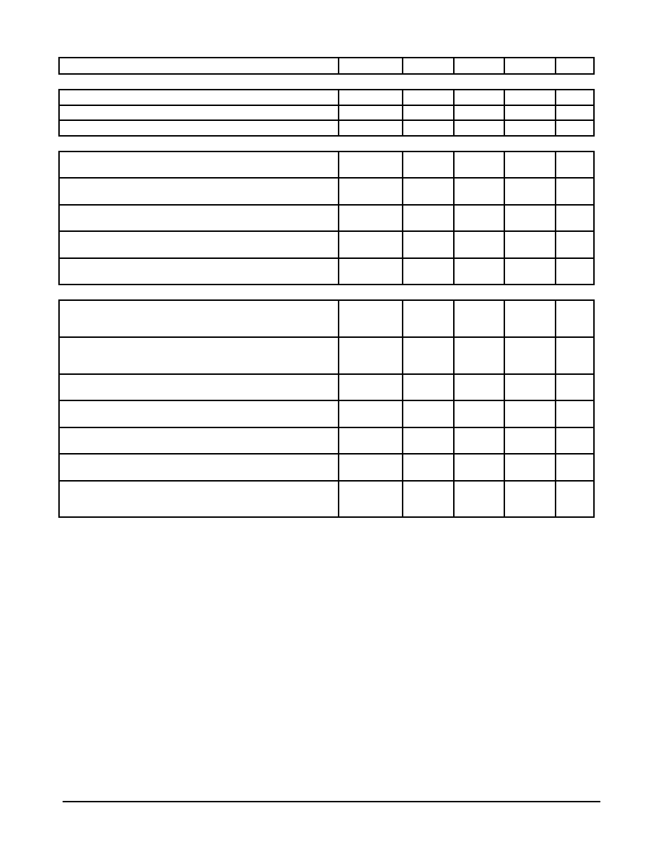
TYPICAL CHARACTERISTICS
TA = 25
∞
C
TA = ≠55
∞
C THRU
+70
∞
C
+100
∞
C
+25
∞
C
Figure 1. LED Forward Voltage versus Forward Current
Figure 2. Output Current versus Input Current
2
1.8
1.6
1.4
1.2
1
1
10
100
1000
IF, LED FORWARD CURRENT (mA)
25
∞
C
100
∞
C
V
F
, FOR
W
ARD VOL
T
AGE (VOL
TS)
I C
, OUTPUT
COLLECT
OR CURRENT
(NORMALIZED)
10
1
0.1
0.01
0.5
1
2
5
10
20
50
IF, LED INPUT CURRENT (mA)
NORMALIZED TO: IF = 10 mA
TA = ≠55
∞
C
PULSE ONLY
PULSE OR DC
20
0
Figure 3. Collector Current versus
Collector≠Emitter Voltage
0
VCE, COLLECTOR≠EMITTER VOLTAGE (VOLTS)
40
60
80
100
120
140
1
2
3
4
5
6
7
8
9
10
5 mA
2 mA
1 mA
10
7
5
2
1
0.7
0.5
0.2
0.1
≠60
Figure 4. Output Current versus Ambient Temperature
≠40
≠20
C
, OUTPUT
COLLECT
OR CURRENT
(NORMALIZED)
0
20
40
60
80
100
TA, AMBIENT TEMPERATURE (
∞
C)
I
≠60
Figure 5. Collector≠Emitter Voltage versus
Ambient Temperature
0.7
TA, AMBIENT TEMPERATURE (
∞
C)
V
CE
, COLLECT
OR≠EMITTER VOL
T
AGE (NORMALIZED)
≠40
≠20
0
20
40
60
80
100
0.8
0.9
1
1.1
1.2
1.3
0
Figure 6. Collector≠Emitter Dark Current versus
Ambient Temperature
1
TA, AMBIENT TEMPERATURE (
∞
C)
I
10
102
103
104
105
20
40
60
80
100
NORMALIZED TO: VCE = 10 V
NORMALIZED TO:
TA = 25
∞
C
30 V
10 V
CEO
, COLLECT
OR≠EMITTER DARK CURRENT
(NORMALIZED)
IF = 10 mA
NORMALIZED TO TA = 25
∞
C
NORMALIZED TO TA = 25
∞
C
CI
, COLLECT
OR CURRENT
(mA)
4N29 4N29A 4N30 4N31 4N32 4N33
4
Motorola Optoelectronics Device Data
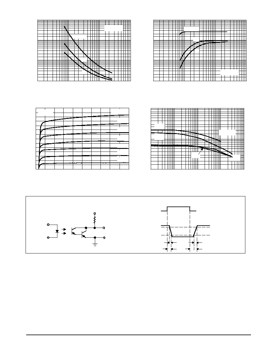
0.1
Figure 7. Turn≠On Switching Times
1
IF, LED INPUT CURRENT (mA)
t,
TIME (
s)
10
100
1000
µ
0.2
0.5
1
2
5
10
20
50
100
RL = 1000
100
10
0.1
1
IF, LED INPUT CURRENT (mA)
10
100
1000
0.2
0.5
1
2
5
10
20
50
100
RL = 1000
100
10
t,
TIME (
s)
µ
Figure 8. Turn≠Off Switching Times
VCC = 10 V
VCC = 10 V
,
TYPICAL
COLLECT
OR CURRENT
(mA)
0
Figure 9. DC Current Gain (Detector Only)
IB = 0.7
µ
A
0
VCE, COLLECTOR≠EMITTER VOLTAGE (VOLTS)
I
2
4
6
8
10
12
14
2
4
6
8
10
12
14
16
18
20
IF = 0
C
0.6
µ
A
0.5
µ
A
0.4
µ
A
0.3
µ
A
0.2
µ
A
0.1
µ
A
0.01
Figure 10. Capacitances versus Voltage
1
V, VOLTAGE (VOLTS)
C, CAP
ACIT
ANCE (pF)
10
100
0.1
1
10
100
CEB
CCB
CLED
f = 1 MHz
CCE
TEST CIRCUIT
VCC = 10 V
IF = 200 mA
INPUT
RL
OUTPUT
WAVEFORMS
10%
90%
ton
INPUT PULSE
OUTPUT PULSE
tf
toff
tr
Figure 11. Switching Time Test Circuit and Waveforms
PULSE WIDTH
< 1 ms
IC = 50 mA

4N29 4N29A 4N30 4N31 4N32 4N33
5
Motorola Optoelectronics Device Data
PACKAGE DIMENSIONS
CASE 730A≠04
ISSUE G
NOTES:
1. DIMENSIONING AND TOLERANCING PER ANSI
Y14.5M, 1982.
2. CONTROLLING DIMENSION: INCH.
3. DIMENSION L TO CENTER OF LEAD WHEN
FORMED PARALLEL.
STYLE 1:
PIN 1. ANODE
2. CATHODE
3. NC
4. EMITTER
5. COLLECTOR
6. BASE
6
4
1
3
≠A≠
≠B≠
SEATING
PLANE
≠T≠
4 PL
F
K
C
N
G
6 PL
D
6 PL
E
M
A
M
0.13 (0.005)
B
M
T
L
M
6 PL
J
M
B
M
0.13 (0.005)
A
M
T
DIM
MIN
MAX
MIN
MAX
MILLIMETERS
INCHES
A
0.320
0.350
8.13
8.89
B
0.240
0.260
6.10
6.60
C
0.115
0.200
2.93
5.08
D
0.016
0.020
0.41
0.50
E
0.040
0.070
1.02
1.77
F
0.010
0.014
0.25
0.36
G
0.100 BSC
2.54 BSC
J
0.008
0.012
0.21
0.30
K
0.100
0.150
2.54
3.81
L
0.300 BSC
7.62 BSC
M
0
15
0
15
N
0.015
0.100
0.38
2.54
_
_
_
_
CASE 730C≠04
ISSUE D
≠A≠
≠B≠
S
SEATING
PLANE
≠T≠
J
K
L
6 PL
M
B
M
0.13 (0.005)
A
M
T
C
D
6 PL
M
A
M
0.13 (0.005)
B
M
T
H
G
E
6 PL
F
4 PL
3
1
4
6
NOTES:
1. DIMENSIONING AND TOLERANCING PER ANSI
Y14.5M, 1982.
2. CONTROLLING DIMENSION: INCH.
DIM
MIN
MAX
MIN
MAX
MILLIMETERS
INCHES
A
0.320
0.350
8.13
8.89
B
0.240
0.260
6.10
6.60
C
0.115
0.200
2.93
5.08
D
0.016
0.020
0.41
0.50
E
0.040
0.070
1.02
1.77
F
0.010
0.014
0.25
0.36
G
0.100 BSC
2.54 BSC
H
0.020
0.025
0.51
0.63
J
0.008
0.012
0.20
0.30
K
0.006
0.035
0.16
0.88
L
0.320 BSC
8.13 BSC
S
0.332
0.390
8.43
9.90
*Consult factory for leadform
option availability