 | ÐлекÑÑоннÑй компоненÑ: BD244B | СкаÑаÑÑ:  PDF PDF  ZIP ZIP |
Äîêóìåíòàöèÿ è îïèñàíèÿ www.docs.chipfind.ru
1
Motorola Bipolar Power Transistor Device Data
Complementary Silicon Plastic
Power Transistors
. . . designed for use in general purpose amplifier and switching applications.
·
Collector Emitter Saturation Voltage --
VCE(sat) = 1.5 Vdc (Max) @ IC = 6.0 Adc
·
Collector Emitter Sustaining Voltage --
VCEO(sus) = 80 Vdc (Min) -- BD243B, BD244B
VCEO(sus)
= 100 Vdc (Min) -- BD243C, BD244C
·
High Current Gain Bandwidth Product
fT = 3.0 MHz (Min) @ IC = 500 mAdc
·
Compact TO220 AB Package
ÎÎÎÎÎÎÎÎÎÎÎÎÎÎÎÎÎÎÎÎÎÎÎ
ÎÎÎÎÎÎÎÎÎÎÎÎÎÎÎÎÎÎÎÎÎÎÎ
ÎÎÎÎÎÎÎÎÎÎÎÎÎÎÎÎÎÎÎÎÎÎÎ
ÎÎÎÎÎÎÎÎÎÎÎÎÎÎÎÎÎÎÎÎÎÎÎ
MAXIMUM RATINGS
ÎÎÎÎÎÎÎÎÎÎÎÎ
ÎÎÎÎÎÎÎÎÎÎÎÎ
ÎÎÎÎÎÎÎÎÎÎÎÎ
ÎÎÎÎÎÎÎÎÎÎÎÎ
ÎÎÎÎÎÎÎÎÎÎÎÎ
Rating
ÎÎÎÎ
ÎÎÎÎ
ÎÎÎÎ
ÎÎÎÎ
ÎÎÎÎ
Symbol
ÎÎÎÎ
ÎÎÎÎ
ÎÎÎÎ
ÎÎÎÎ
ÎÎÎÎ
BD243B
BD244B
ÎÎÎÎ
ÎÎÎÎ
ÎÎÎÎ
ÎÎÎÎ
ÎÎÎÎ
BD243C
BD244C
ÎÎÎ
ÎÎÎ
ÎÎÎ
ÎÎÎ
ÎÎÎ
Unit
ÎÎÎÎÎÎÎÎÎÎÎÎ
ÎÎÎÎÎÎÎÎÎÎÎÎ
ÎÎÎÎÎÎÎÎÎÎÎÎ
ÎÎÎÎÎÎÎÎÎÎÎÎ
CollectorEmitter Voltage
ÎÎÎÎ
ÎÎÎÎ
ÎÎÎÎ
ÎÎÎÎ
VCEO
ÎÎÎÎ
ÎÎÎÎ
ÎÎÎÎ
ÎÎÎÎ
80
ÎÎÎÎ
ÎÎÎÎ
ÎÎÎÎ
ÎÎÎÎ
100
ÎÎÎ
ÎÎÎ
ÎÎÎ
ÎÎÎ
Vdc
ÎÎÎÎÎÎÎÎÎÎÎÎ
ÎÎÎÎÎÎÎÎÎÎÎÎ
ÎÎÎÎÎÎÎÎÎÎÎÎ
ÎÎÎÎÎÎÎÎÎÎÎÎ
CollectorBase Voltage
ÎÎÎÎ
ÎÎÎÎ
ÎÎÎÎ
ÎÎÎÎ
VCB
ÎÎÎÎ
ÎÎÎÎ
ÎÎÎÎ
ÎÎÎÎ
80
ÎÎÎÎ
ÎÎÎÎ
ÎÎÎÎ
ÎÎÎÎ
100
ÎÎÎ
ÎÎÎ
ÎÎÎ
ÎÎÎ
Vdc
ÎÎÎÎÎÎÎÎÎÎÎÎ
ÎÎÎÎÎÎÎÎÎÎÎÎ
ÎÎÎÎÎÎÎÎÎÎÎÎ
ÎÎÎÎÎÎÎÎÎÎÎÎ
EmitterBase Voltage
ÎÎÎÎ
ÎÎÎÎ
ÎÎÎÎ
ÎÎÎÎ
VEB
ÎÎÎÎÎÎÎ
ÎÎÎÎÎÎÎ
ÎÎÎÎÎÎÎ
ÎÎÎÎÎÎÎ
5.0
ÎÎÎ
ÎÎÎ
ÎÎÎ
ÎÎÎ
Vdc
ÎÎÎÎÎÎÎÎÎÎÎÎ
ÎÎÎÎÎÎÎÎÎÎÎÎ
ÎÎÎÎÎÎÎÎÎÎÎÎ
ÎÎÎÎÎÎÎÎÎÎÎÎ
ÎÎÎÎÎÎÎÎÎÎÎÎ
Collector Current -- Continuous
Peak
ÎÎÎÎ
ÎÎÎÎ
ÎÎÎÎ
ÎÎÎÎ
ÎÎÎÎ
IC
ÎÎÎÎÎÎÎ
ÎÎÎÎÎÎÎ
ÎÎÎÎÎÎÎ
ÎÎÎÎÎÎÎ
ÎÎÎÎÎÎÎ
6
10
ÎÎÎ
ÎÎÎ
ÎÎÎ
ÎÎÎ
ÎÎÎ
Adc
ÎÎÎÎÎÎÎÎÎÎÎÎ
ÎÎÎÎÎÎÎÎÎÎÎÎ
ÎÎÎÎÎÎÎÎÎÎÎÎ
ÎÎÎÎÎÎÎÎÎÎÎÎ
Base Current
ÎÎÎÎ
ÎÎÎÎ
ÎÎÎÎ
ÎÎÎÎ
IB
ÎÎÎÎÎÎÎ
ÎÎÎÎÎÎÎ
ÎÎÎÎÎÎÎ
ÎÎÎÎÎÎÎ
2.0
ÎÎÎ
ÎÎÎ
ÎÎÎ
ÎÎÎ
Adc
ÎÎÎÎÎÎÎÎÎÎÎÎ
ÎÎÎÎÎÎÎÎÎÎÎÎ
ÎÎÎÎÎÎÎÎÎÎÎÎ
ÎÎÎÎÎÎÎÎÎÎÎÎ
ÎÎÎÎÎÎÎÎÎÎÎÎ
Total Device Dissipation
@ TC = 25
_
C
Derate above 25
_
C
ÎÎÎÎ
ÎÎÎÎ
ÎÎÎÎ
ÎÎÎÎ
ÎÎÎÎ
PD
ÎÎÎÎÎÎÎ
ÎÎÎÎÎÎÎ
ÎÎÎÎÎÎÎ
ÎÎÎÎÎÎÎ
ÎÎÎÎÎÎÎ
65
0.52
ÎÎÎ
ÎÎÎ
ÎÎÎ
ÎÎÎ
ÎÎÎ
Watts
W/
_
C
ÎÎÎÎÎÎÎÎÎÎÎÎ
ÎÎÎÎÎÎÎÎÎÎÎÎ
ÎÎÎÎÎÎÎÎÎÎÎÎ
ÎÎÎÎÎÎÎÎÎÎÎÎ
ÎÎÎÎÎÎÎÎÎÎÎÎ
Operating and Storage Junction
Temperature Range
ÎÎÎÎ
ÎÎÎÎ
ÎÎÎÎ
ÎÎÎÎ
ÎÎÎÎ
TJ, Tstg
ÎÎÎÎÎÎÎ
ÎÎÎÎÎÎÎ
ÎÎÎÎÎÎÎ
ÎÎÎÎÎÎÎ
ÎÎÎÎÎÎÎ
65 to + 150
ÎÎÎ
ÎÎÎ
ÎÎÎ
ÎÎÎ
ÎÎÎ
_
C
ÎÎÎÎÎÎÎÎÎÎÎÎÎÎÎÎÎÎÎÎÎÎÎ
ÎÎÎÎÎÎÎÎÎÎÎÎÎÎÎÎÎÎÎÎÎÎÎ
ÎÎÎÎÎÎÎÎÎÎÎÎÎÎÎÎÎÎÎÎÎÎÎ
ÎÎÎÎÎÎÎÎÎÎÎÎÎÎÎÎÎÎÎÎÎÎÎ
THERMAL CHARACTERISTICS
ÎÎÎÎÎÎÎÎÎÎÎÎ
ÎÎÎÎÎÎÎÎÎÎÎÎ
ÎÎÎÎÎÎÎÎÎÎÎÎ
ÎÎÎÎÎÎÎÎÎÎÎÎ
Characteristic
ÎÎÎÎÎ
ÎÎÎÎÎ
ÎÎÎÎÎ
ÎÎÎÎÎ
Symbol
ÎÎÎÎÎÎ
ÎÎÎÎÎÎ
ÎÎÎÎÎÎ
ÎÎÎÎÎÎ
Max
ÎÎÎ
ÎÎÎ
ÎÎÎ
ÎÎÎ
Unit
ÎÎÎÎÎÎÎÎÎÎÎÎ
ÎÎÎÎÎÎÎÎÎÎÎÎ
ÎÎÎÎÎÎÎÎÎÎÎÎ
ÎÎÎÎÎÎÎÎÎÎÎÎ
Thermal Resistance, Junction to Case
ÎÎÎÎÎ
ÎÎÎÎÎ
ÎÎÎÎÎ
ÎÎÎÎÎ
R
JC
ÎÎÎÎÎÎ
ÎÎÎÎÎÎ
ÎÎÎÎÎÎ
ÎÎÎÎÎÎ
1.92
ÎÎÎ
ÎÎÎ
ÎÎÎ
ÎÎÎ
_
C/W
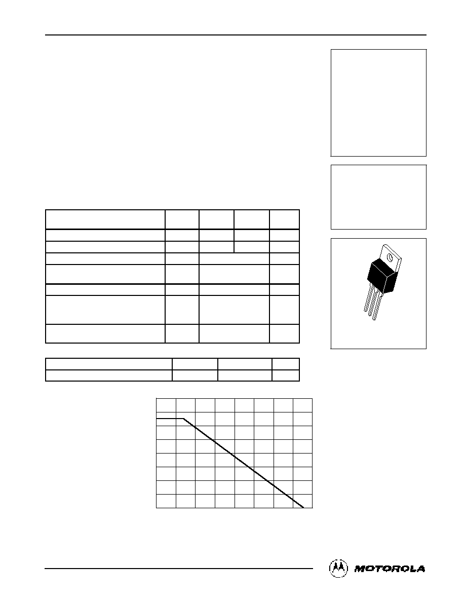
80
60
40
20
0
0
20
40
60
80
100
120
140
160
Figure 1. Power Derating
TC, CASE TEMPERATURE (
°
C)
P
D
, POWER DISSIP
A
TION (W
A
TTS)
Preferred devices are Motorola recommended choices for future use and best overall value.
MOTOROLA
SEMICONDUCTOR TECHNICAL DATA
Order this document
by BD243B/D
©
Motorola, Inc. 1995
BD243B
BD243C
BD244B
BD244C
6 AMPERE
POWER TRANSISTORS
COMPLEMENTARY
SILICON
80 100 VOLTS
65 WATTS
*Motorola Preferred Device
CASE 221A06
TO220AB
NPN
PNP
*
*
REV 7
BD243B BD243C BD244B BD244C
2
Motorola Bipolar Power Transistor Device Data
ÎÎÎÎÎÎÎÎÎÎÎÎÎÎÎÎÎÎÎÎÎÎÎÎÎÎÎÎÎÎÎÎÎÎ
ÎÎÎÎÎÎÎÎÎÎÎÎÎÎÎÎÎÎÎÎÎÎÎÎÎÎÎÎÎÎÎÎÎÎ
ÎÎÎÎÎÎÎÎÎÎÎÎÎÎÎÎÎÎÎÎÎÎÎÎÎÎÎÎÎÎÎÎÎÎ
ÎÎÎÎÎÎÎÎÎÎÎÎÎÎÎÎÎÎÎÎÎÎÎÎÎÎÎÎÎÎÎÎÎÎ
ELECTRICAL CHARACTERISTICS
(TC = 25
_
C unless otherwise noted)
ÎÎÎÎÎÎÎÎÎÎÎÎÎÎÎÎÎÎÎÎÎÎÎ
ÎÎÎÎÎÎÎÎÎÎÎÎÎÎÎÎÎÎÎÎÎÎÎ
ÎÎÎÎÎÎÎÎÎÎÎÎÎÎÎÎÎÎÎÎÎÎÎ
ÎÎÎÎÎÎÎÎÎÎÎÎÎÎÎÎÎÎÎÎÎÎÎ
Characteristic
ÎÎÎÎ
ÎÎÎÎ
ÎÎÎÎ
ÎÎÎÎ
Symbol
ÎÎÎÎ
ÎÎÎÎ
ÎÎÎÎ
ÎÎÎÎ
Min
ÎÎÎÎ
ÎÎÎÎ
ÎÎÎÎ
ÎÎÎÎ
Max
ÎÎÎ
ÎÎÎ
ÎÎÎ
ÎÎÎ
Unit
ÎÎÎÎÎÎÎÎÎÎÎÎÎÎÎÎÎÎÎÎÎÎÎ
ÎÎÎÎÎÎÎÎÎÎÎÎÎÎÎÎÎÎÎÎÎÎÎ
ÎÎÎÎÎÎÎÎÎÎÎÎÎÎÎÎÎÎÎÎÎÎÎ
ÎÎÎÎÎÎÎÎÎÎÎÎÎÎÎÎÎÎÎÎÎÎÎ
CollectorEmitter Sustaining Voltage (1)
(IC = 30 mAdc, IB = 0)
BD243B, BD244B
BD243C, BD244C
ÎÎÎÎ
ÎÎÎÎ
ÎÎÎÎ
ÎÎÎÎ
VCEO(sus)
ÎÎÎÎ
ÎÎÎÎ
ÎÎÎÎ
ÎÎÎÎ
80
100
ÎÎÎÎ
ÎÎÎÎ
ÎÎÎÎ
ÎÎÎÎ
--
--
ÎÎÎ
ÎÎÎ
ÎÎÎ
ÎÎÎ
Vdc
ÎÎÎÎÎÎÎÎÎÎÎÎÎÎÎÎÎÎÎÎÎÎÎ
ÎÎÎÎÎÎÎÎÎÎÎÎÎÎÎÎÎÎÎÎÎÎÎ
ÎÎÎÎÎÎÎÎÎÎÎÎÎÎÎÎÎÎÎÎÎÎÎ
ÎÎÎÎÎÎÎÎÎÎÎÎÎÎÎÎÎÎÎÎÎÎÎ
ÎÎÎÎÎÎÎÎÎÎÎÎÎÎÎÎÎÎÎÎÎÎÎ
(IC = 30 mAdc, IB = 0)
BD243B, BD244B
BD243C, BD244C
ÎÎÎÎ
ÎÎÎÎ
ÎÎÎÎ
ÎÎÎÎ
ÎÎÎÎ
ÎÎÎÎ
ÎÎÎÎ
ÎÎÎÎ
ÎÎÎÎ
ÎÎÎÎ
80
100
ÎÎÎÎ
ÎÎÎÎ
ÎÎÎÎ
ÎÎÎÎ
ÎÎÎÎ
--
--
ÎÎÎ
ÎÎÎ
ÎÎÎ
ÎÎÎ
ÎÎÎ
ÎÎÎÎÎÎÎÎÎÎÎÎÎÎÎÎÎÎÎÎÎÎÎ
ÎÎÎÎÎÎÎÎÎÎÎÎÎÎÎÎÎÎÎÎÎÎÎ
ÎÎÎÎÎÎÎÎÎÎÎÎÎÎÎÎÎÎÎÎÎÎÎ
ÎÎÎÎÎÎÎÎÎÎÎÎÎÎÎÎÎÎÎÎÎÎÎ
Collector Cutoff Current
(VCE = 60 Vdc, IB = 0)
BD243B, BD243C, BD244B, BD244C
ÎÎÎÎ
ÎÎÎÎ
ÎÎÎÎ
ÎÎÎÎ
ICEO
ÎÎÎÎ
ÎÎÎÎ
ÎÎÎÎ
ÎÎÎÎ
--
ÎÎÎÎ
ÎÎÎÎ
ÎÎÎÎ
ÎÎÎÎ
0.7
ÎÎÎ
ÎÎÎ
ÎÎÎ
ÎÎÎ
mAdc
ÎÎÎÎÎÎÎÎÎÎÎÎÎÎÎÎÎÎÎÎÎÎÎ
ÎÎÎÎÎÎÎÎÎÎÎÎÎÎÎÎÎÎÎÎÎÎÎ
ÎÎÎÎÎÎÎÎÎÎÎÎÎÎÎÎÎÎÎÎÎÎÎ
ÎÎÎÎÎÎÎÎÎÎÎÎÎÎÎÎÎÎÎÎÎÎÎ
ÎÎÎÎÎÎÎÎÎÎÎÎÎÎÎÎÎÎÎÎÎÎÎ
ÎÎÎÎÎÎÎÎÎÎÎÎÎÎÎÎÎÎÎÎÎÎÎ
Collector Cutoff Current
(VCE = 80 Vdc, VEB = 0)
BD243B, BD244B
(VCE = 100 Vdc, VEB = 0)
BD243C, BD244C
ÎÎÎÎ
ÎÎÎÎ
ÎÎÎÎ
ÎÎÎÎ
ÎÎÎÎ
ÎÎÎÎ
ICES
ÎÎÎÎ
ÎÎÎÎ
ÎÎÎÎ
ÎÎÎÎ
ÎÎÎÎ
ÎÎÎÎ
--
--
ÎÎÎÎ
ÎÎÎÎ
ÎÎÎÎ
ÎÎÎÎ
ÎÎÎÎ
ÎÎÎÎ
400
400
ÎÎÎ
ÎÎÎ
ÎÎÎ
ÎÎÎ
ÎÎÎ
ÎÎÎ
µ
Adc
ÎÎÎÎÎÎÎÎÎÎÎÎÎÎÎÎÎÎÎÎÎÎÎ
ÎÎÎÎÎÎÎÎÎÎÎÎÎÎÎÎÎÎÎÎÎÎÎ
ÎÎÎÎÎÎÎÎÎÎÎÎÎÎÎÎÎÎÎÎÎÎÎ
ÎÎÎÎÎÎÎÎÎÎÎÎÎÎÎÎÎÎÎÎÎÎÎ
Emitter Cutoff Current
(VBE = 5.0 Vdc, IC = 0)
ÎÎÎÎ
ÎÎÎÎ
ÎÎÎÎ
ÎÎÎÎ
IEBO
ÎÎÎÎ
ÎÎÎÎ
ÎÎÎÎ
ÎÎÎÎ
--
ÎÎÎÎ
ÎÎÎÎ
ÎÎÎÎ
ÎÎÎÎ
1.0
ÎÎÎ
ÎÎÎ
ÎÎÎ
ÎÎÎ
mAdc
ÎÎÎÎÎÎÎÎÎÎÎÎÎÎÎÎÎÎÎÎÎÎÎÎÎÎÎÎÎÎÎÎÎÎ
ÎÎÎÎÎÎÎÎÎÎÎÎÎÎÎÎÎÎÎÎÎÎÎÎÎÎÎÎÎÎÎÎÎÎ
ÎÎÎÎÎÎÎÎÎÎÎÎÎÎÎÎÎÎÎÎÎÎÎÎÎÎÎÎÎÎÎÎÎÎ
ÎÎÎÎÎÎÎÎÎÎÎÎÎÎÎÎÎÎÎÎÎÎÎÎÎÎÎÎÎÎÎÎÎÎ
ON CHARACTERISTICS (1)
ÎÎÎÎÎÎÎÎÎÎÎÎÎÎÎÎÎÎÎÎÎÎÎ
ÎÎÎÎÎÎÎÎÎÎÎÎÎÎÎÎÎÎÎÎÎÎÎ
ÎÎÎÎÎÎÎÎÎÎÎÎÎÎÎÎÎÎÎÎÎÎÎ
ÎÎÎÎÎÎÎÎÎÎÎÎÎÎÎÎÎÎÎÎÎÎÎ
ÎÎÎÎÎÎÎÎÎÎÎÎÎÎÎÎÎÎÎÎÎÎÎ
ÎÎÎÎÎÎÎÎÎÎÎÎÎÎÎÎÎÎÎÎÎÎÎ
DC Current Gain
(IC = 0.3 Adc, VCE = 4.0 Vdc)
(IC = 3.0 Adc, VCE = 4.0 Vdc)
ÎÎÎÎ
ÎÎÎÎ
ÎÎÎÎ
ÎÎÎÎ
ÎÎÎÎ
ÎÎÎÎ
hFE
ÎÎÎÎ
ÎÎÎÎ
ÎÎÎÎ
ÎÎÎÎ
ÎÎÎÎ
ÎÎÎÎ
30
15
ÎÎÎÎ
ÎÎÎÎ
ÎÎÎÎ
ÎÎÎÎ
ÎÎÎÎ
ÎÎÎÎ
--
--
ÎÎÎ
ÎÎÎ
ÎÎÎ
ÎÎÎ
ÎÎÎ
ÎÎÎ
--
ÎÎÎÎÎÎÎÎÎÎÎÎÎÎÎÎÎÎÎÎÎÎÎ
ÎÎÎÎÎÎÎÎÎÎÎÎÎÎÎÎÎÎÎÎÎÎÎ
ÎÎÎÎÎÎÎÎÎÎÎÎÎÎÎÎÎÎÎÎÎÎÎ
ÎÎÎÎÎÎÎÎÎÎÎÎÎÎÎÎÎÎÎÎÎÎÎ
CollectorEmitter Saturation Voltage
(IC = 6.0 Adc, IB = 1.0 Adc)
ÎÎÎÎ
ÎÎÎÎ
ÎÎÎÎ
ÎÎÎÎ
VCE(sat)
ÎÎÎÎ
ÎÎÎÎ
ÎÎÎÎ
ÎÎÎÎ
--
ÎÎÎÎ
ÎÎÎÎ
ÎÎÎÎ
ÎÎÎÎ
1.5
ÎÎÎ
ÎÎÎ
ÎÎÎ
ÎÎÎ
Vdc
ÎÎÎÎÎÎÎÎÎÎÎÎÎÎÎÎÎÎÎÎÎÎÎ
ÎÎÎÎÎÎÎÎÎÎÎÎÎÎÎÎÎÎÎÎÎÎÎ
ÎÎÎÎÎÎÎÎÎÎÎÎÎÎÎÎÎÎÎÎÎÎÎ
ÎÎÎÎÎÎÎÎÎÎÎÎÎÎÎÎÎÎÎÎÎÎÎ
ÎÎÎÎÎÎÎÎÎÎÎÎÎÎÎÎÎÎÎÎÎÎÎ
BaseEmitter On Voltage
(IC = 6.0 Adc, VCE = 4.0 Vdc)
ÎÎÎÎ
ÎÎÎÎ
ÎÎÎÎ
ÎÎÎÎ
ÎÎÎÎ
VBE(on)
ÎÎÎÎ
ÎÎÎÎ
ÎÎÎÎ
ÎÎÎÎ
ÎÎÎÎ
--
ÎÎÎÎ
ÎÎÎÎ
ÎÎÎÎ
ÎÎÎÎ
ÎÎÎÎ
2.0
ÎÎÎ
ÎÎÎ
ÎÎÎ
ÎÎÎ
ÎÎÎ
Vdc
ÎÎÎÎÎÎÎÎÎÎÎÎÎÎÎÎÎÎÎÎÎÎÎÎÎÎÎÎÎÎÎÎÎÎ
ÎÎÎÎÎÎÎÎÎÎÎÎÎÎÎÎÎÎÎÎÎÎÎÎÎÎÎÎÎÎÎÎÎÎ
ÎÎÎÎÎÎÎÎÎÎÎÎÎÎÎÎÎÎÎÎÎÎÎÎÎÎÎÎÎÎÎÎÎÎ
ÎÎÎÎÎÎÎÎÎÎÎÎÎÎÎÎÎÎÎÎÎÎÎÎÎÎÎÎÎÎÎÎÎÎ
DYNAMIC CHARACTERISTICS
ÎÎÎÎÎÎÎÎÎÎÎÎÎÎÎÎÎÎÎÎÎÎÎ
ÎÎÎÎÎÎÎÎÎÎÎÎÎÎÎÎÎÎÎÎÎÎÎ
ÎÎÎÎÎÎÎÎÎÎÎÎÎÎÎÎÎÎÎÎÎÎÎ
ÎÎÎÎÎÎÎÎÎÎÎÎÎÎÎÎÎÎÎÎÎÎÎ
ÎÎÎÎÎÎÎÎÎÎÎÎÎÎÎÎÎÎÎÎÎÎÎ
CurrentGain -- Bandwidth Product (2)
(IC = 500 mAdc, VCE = 10 Vdc, ftest = 1.0 MHz)
ÎÎÎÎ
ÎÎÎÎ
ÎÎÎÎ
ÎÎÎÎ
ÎÎÎÎ
fT
ÎÎÎÎ
ÎÎÎÎ
ÎÎÎÎ
ÎÎÎÎ
ÎÎÎÎ
3.0
ÎÎÎÎ
ÎÎÎÎ
ÎÎÎÎ
ÎÎÎÎ
ÎÎÎÎ
--
ÎÎÎ
ÎÎÎ
ÎÎÎ
ÎÎÎ
ÎÎÎ
MHz
ÎÎÎÎÎÎÎÎÎÎÎÎÎÎÎÎÎÎÎÎÎÎÎ
ÎÎÎÎÎÎÎÎÎÎÎÎÎÎÎÎÎÎÎÎÎÎÎ
ÎÎÎÎÎÎÎÎÎÎÎÎÎÎÎÎÎÎÎÎÎÎÎ
ÎÎÎÎÎÎÎÎÎÎÎÎÎÎÎÎÎÎÎÎÎÎÎ
SmallSignal Current Gain
(IC = 0.5 Adc, VCE = 10 Vdc, f = 1.0 kHz)
ÎÎÎÎ
ÎÎÎÎ
ÎÎÎÎ
ÎÎÎÎ
hfe
ÎÎÎÎ
ÎÎÎÎ
ÎÎÎÎ
ÎÎÎÎ
20
ÎÎÎÎ
ÎÎÎÎ
ÎÎÎÎ
ÎÎÎÎ
--
ÎÎÎ
ÎÎÎ
ÎÎÎ
ÎÎÎ
--
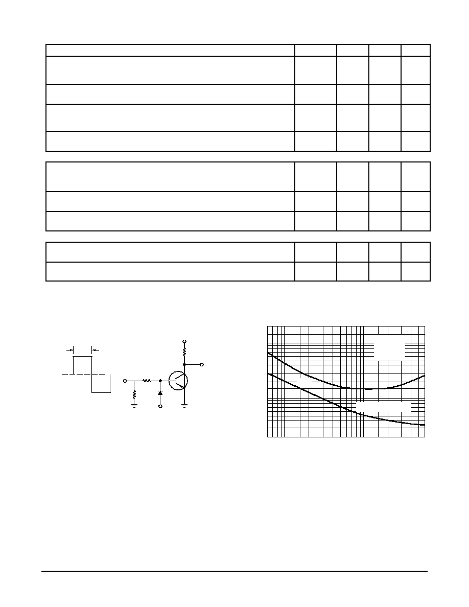
(1) Pulse Test: Pulsewidth
v
300
µ
s, Duty Cycle
v
2.0%.
(2) fT = hfe
·
ftest
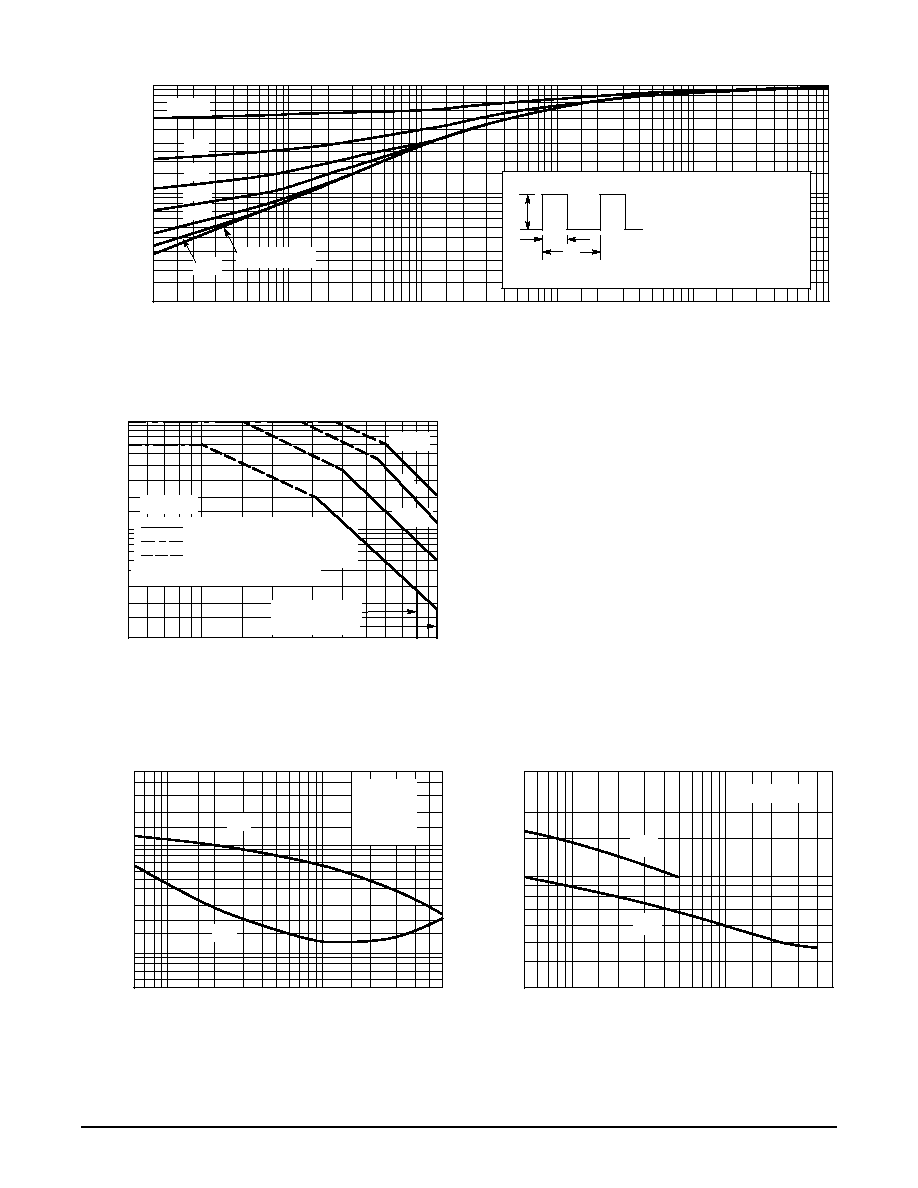
Figure 2. Switching Time Test Circuit
2.0
0.06
Figure 3. TurnOn Time
IC, COLLECTOR CURRENT (AMP)
t,
TIME (
s)
µ
1.0
0.7
0.5
0.3
0.1
0.07
0.02
0.1
0.2
0.4
0.6
2.0
6.0
td @ VBE(off) = 5.0 V
TJ = 25
°
C
VCC = 30 V
IC/IB = 10
+ 11 V
0
VCC
30 V
SCOPE
RB
4 V
tr, tf
v
10 ns
DUTY CYCLE = 1.0%
RC
tr
0.03
0.05
1.0
4.0
D1 MUST BE FAST RECOVERY TYPE eg.
1N5825 USED ABOVE IB
[
100 mA
MSD6100 USED BELOW IB
[
100 mA
25
µ
s
9.0 V
D1
51
RB AND RC VARIED TO OBTAIN DESIRED CURRENT LEVELS
0.2
BD243B BD243C BD244B BD244C
3
Motorola Bipolar Power Transistor Device Data
Figure 4. Thermal Response
t, TIME OR PULSE WIDTH (ms)
1.0
0.01
0.01
0.7
0.5
0.3
0.2
0.1
0.07
0.05
0.03
0.02
0.02
r(t) EFFECTIVE
TRANSIENT
THERMAL
RESIST
ANCE (NORMALIZED)
0.05
0.1
0.2
0.5
1.0
2.0
5.0
10
20
50
100
200
1000
500
R
JC(max) = 1.92
°
C/W
D CURVES APPLY FOR POWER
PULSE TRAIN SHOWN
READ TIME AT t1
TJ(pk) TC = P(pk) R
JC(t)
P(pk)
t1
t2
DUTY CYCLE, D = t1/t2
D = 0.5
SINGLE PULSE
0.2
0.05
0.1
0.02
0.01
SINGLE
PULSE
0.03
0.3
3.0
30
300
SECOND BREAKDOWN LIMITED
BONDING WIRE LIMITED
THERMAL LIMITATION @ TC = 25
°
C
CURVES APPLY BELOW RATED VCEO
10
5.0
Figure 5. Active Region Safe Operating Area
5.0
1.0
0.1
10
20
60
100
TJ = 150
°
C
BD243B, BD244B
BD243C, BD244C
5.0 ms
0.5 ms
0.2
2.0
0.5
I C
, COLLECT
OR CURRENT
(AMP)
VCE, COLLECTOREMITTER VOLTAGE (VOLTS)
3.0
0.3
40
80
1.0
ms
There are two limitations on the power handling ability of a
transistor: average junction temperature and second break-
down. Safe operating area curves indicate IC VCE limits of
the transistor that must be observed for reliable operation,
i.e., the transistor must not be subjected to greater dissipa-
tion than the curves indicate.
The data of Figure 5 is based on TJ(pk) = 150
_
C: TC is
variable depending on conditions. Second breakdown pulse
limits are valid for duty cycles to 10% provided TJ(pk)
v
150
_
C, TJ(pk) may be calculated from the data in Fig-
ure 4. At high case temperatures, thermal limitations will
reduce the power that can be handled to values less than the
limitations imposed by second breakdown.
5.0
0.06
Figure 6. Turn-Off Time
IC, COLLECTOR CURRENT (AMP)
t,
TIME (
s)
µ
2.0
1.0
0.5
0.3
0.2
0.1
0.07
0.05
0.1
0.2
0.4
0.6
2.0
6.0
TJ = 25
°
C
VCC = 30 V
IC/IB = 10
IB1 = IB2
ts
1.0
4.0
0.7
3.0
tf
300
0.5
Figure 7. Capacitance
VR, REVERSE VOLTAGE (VOLTS)
30
1.0
2.0
3.0
5.0
20
30
50
10
CAP
ACIT
ANCE (pF)
200
100
70
50
TJ = 25
°
C
Cib
Cob
BD243B BD243C BD244B BD244C
4
Motorola Bipolar Power Transistor Device Data
V
CE
, COLLECT
OREMITTER VOL
T
AGE (VOL
TS)
500
0.06
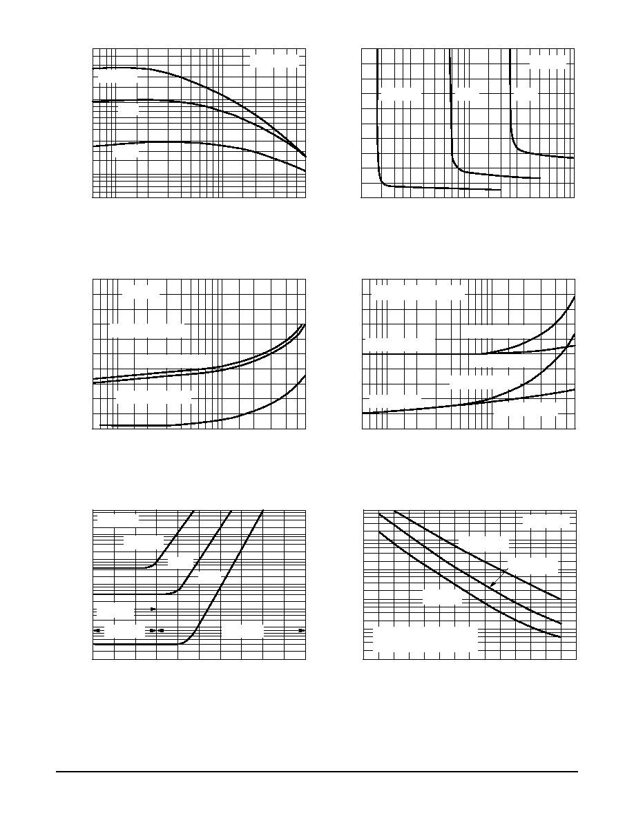
Figure 8. DC Current Gain
IC, COLLECTOR CURRENT (AMP)
5.0
0.1
0.2
0.3 0.4
0.6
1.0
2.0
6.0
100
50
30
10
2.0
0.06
Figure 9. Collector Saturation Region
IC, COLLECTOR CURRENT (AMPS)
0.2
0.3
0.6
2.0 3.0 4.0
6.0
0.8
0.4
0
TJ = 25
°
C
VBE(sat) @ IC/IB = 10
VCE(sat) @ IC/IB = 10
V
, VOL
T
AGE (VOL
TS)
2.0
10
Figure 10. "On" Voltages
IB, BASE CURRENT (mA)
0
20
30
50
100
200 300
500
1000
1.6
1.2
0.8
0.4
IC = 1.0 A
TJ = 25
°
C
2.5 A
5.0 A
300
70
h
FE
, DC CURRENT
GAIN
TJ = 150
°
C
25
°
C
55
°
C
VCE = 2.0 V
+ 2.5
0.06
Figure 11. Temperature Coefficients
IC, COLLECTOR CURRENT (AMP)
0.2
0.3
0.5
1.0
3.0 0.4
0.6
V
,
TEMPERA
TURE COEFFICIENTS (mV/
C)
°
+ 2.0
+ 1.5
+ 0.5
0
0.5
1.0
1.5
2.0
2.5
VB FOR VBE
*
VC FOR VCE(sat)
*APPLIES FOR IC/IB
5.0
103
Figure 12. Collector Cut-Off Region
VBE, BASE-EMITTER VOLTAGE (VOLTS)
102
101
100
101
, COLLECT
OR CURRENT
(
A)
µ
I C 10
2
10 3
0.3 0.2 0.1
0
+ 0.1 + 0.2 + 0.3
+ 0.4 + 0.5 + 0.6
VCE = 30 V
TJ = 150
°
C
100
°
C
REVERSE
FORWARD
IC = ICES
10M
Figure 13. Effects of BaseEmitter Resistance
TJ, JUNCTION TEMPERATURE (
°
C)
20
40
60
80
100
120
140
160
1.0M
100k
R
BE
, EXTERNAL
BASEEMITTER RESIST
ANCE (OHMS)
VCE = 30 V
IC = 10 x ICES
IC
ICES
(TYPICAL ICES VALUES
OBTAINED FROM FIGURE 12)
7.0
0.1
1.0
0.4
1.6
1.2
VBE @ VCE = 4.0 V
+ 1.0
2.0
0.1
IC = 2 x ICES
200
20
4.0
+ 25
°
C to + 150
°
C
55
°
C to + 25
°
C
+ 25
°
C to + 150
°
C
55
°
C to + 25
°
C
25
°
C
+ 0.7
10k
1.0k
0.1k
BD243B BD243C BD244B BD244C
5
Motorola Bipolar Power Transistor Device Data
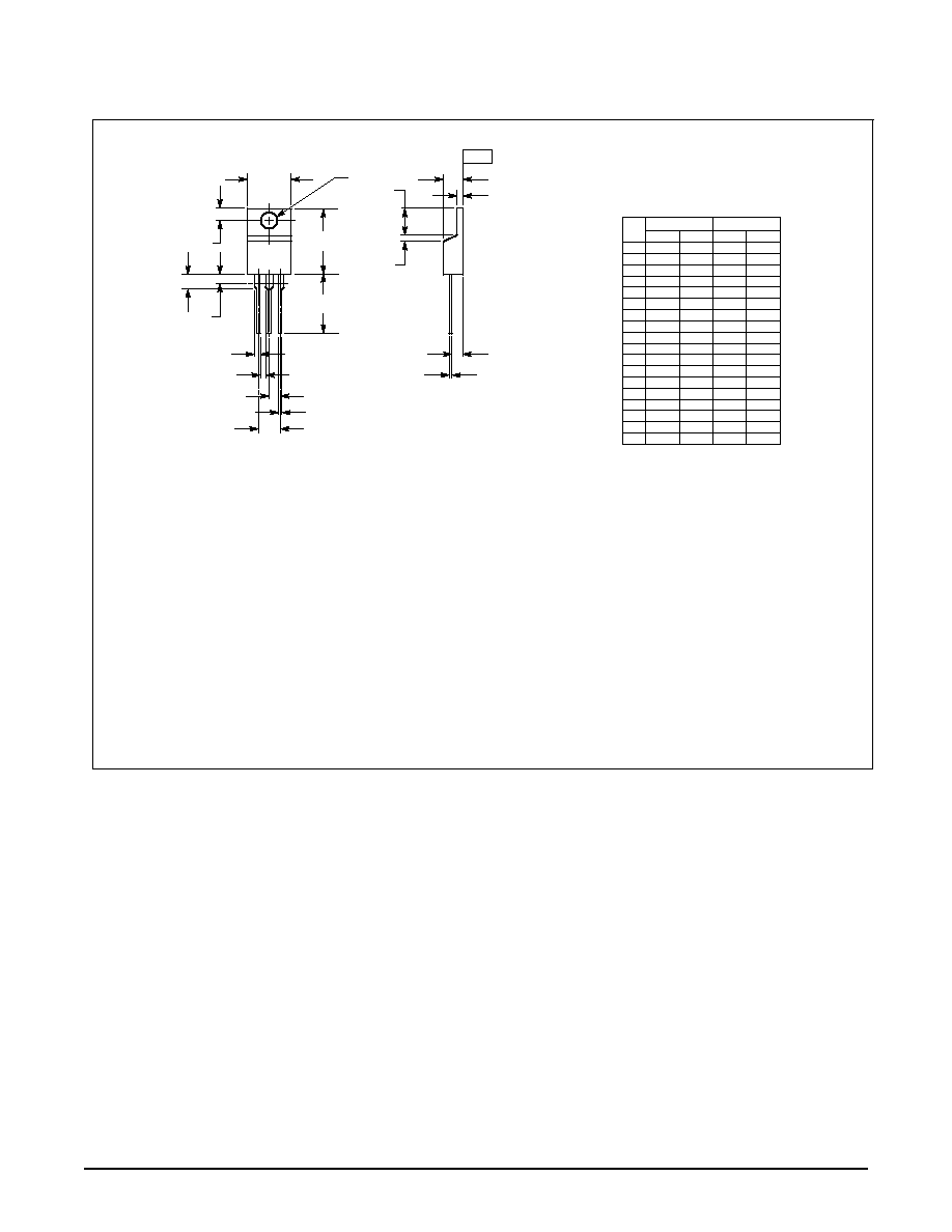
PACKAGE DIMENSIONS
CASE 221A06
TO220AB
ISSUE Y
NOTES:
1. DIMENSIONING AND TOLERANCING PER ANSI
Y14.5M, 1982.
2. CONTROLLING DIMENSION: INCH.
3. DIMENSION Z DEFINES A ZONE WHERE ALL
BODY AND LEAD IRREGULARITIES ARE
ALLOWED.
STYLE 1:
PIN 1. BASE
2. COLLECTOR
3. EMITTER
4. COLLECTOR
DIM
MIN
MAX
MIN
MAX
MILLIMETERS
INCHES
A
0.570
0.620
14.48
15.75
B
0.380
0.405
9.66
10.28
C
0.160
0.190
4.07
4.82
D
0.025
0.035
0.64
0.88
F
0.142
0.147
3.61
3.73
G
0.095
0.105
2.42
2.66
H
0.110
0.155
2.80
3.93
J
0.018
0.025
0.46
0.64
K
0.500
0.562
12.70
14.27
L
0.045
0.060
1.15
1.52
N
0.190
0.210
4.83
5.33
Q
0.100
0.120
2.54
3.04
R
0.080
0.110
2.04
2.79
S
0.045
0.055
1.15
1.39
T
0.235
0.255
5.97
6.47
U
0.000
0.050
0.00
1.27
V
0.045
1.15
Z
0.080
2.04
B
Q
H
Z
L
V
G
N
A
K
F
1
2 3
4
D
SEATING
PLANE
T
C
S
T
U
R
J