 | ÐлекÑÑоннÑй компоненÑ: c74ac244 | СкаÑаÑÑ:  PDF PDF  ZIP ZIP |
Äîêóìåíòàöèÿ è îïèñàíèÿ www.docs.chipfind.ru
5-1
FACT DATA
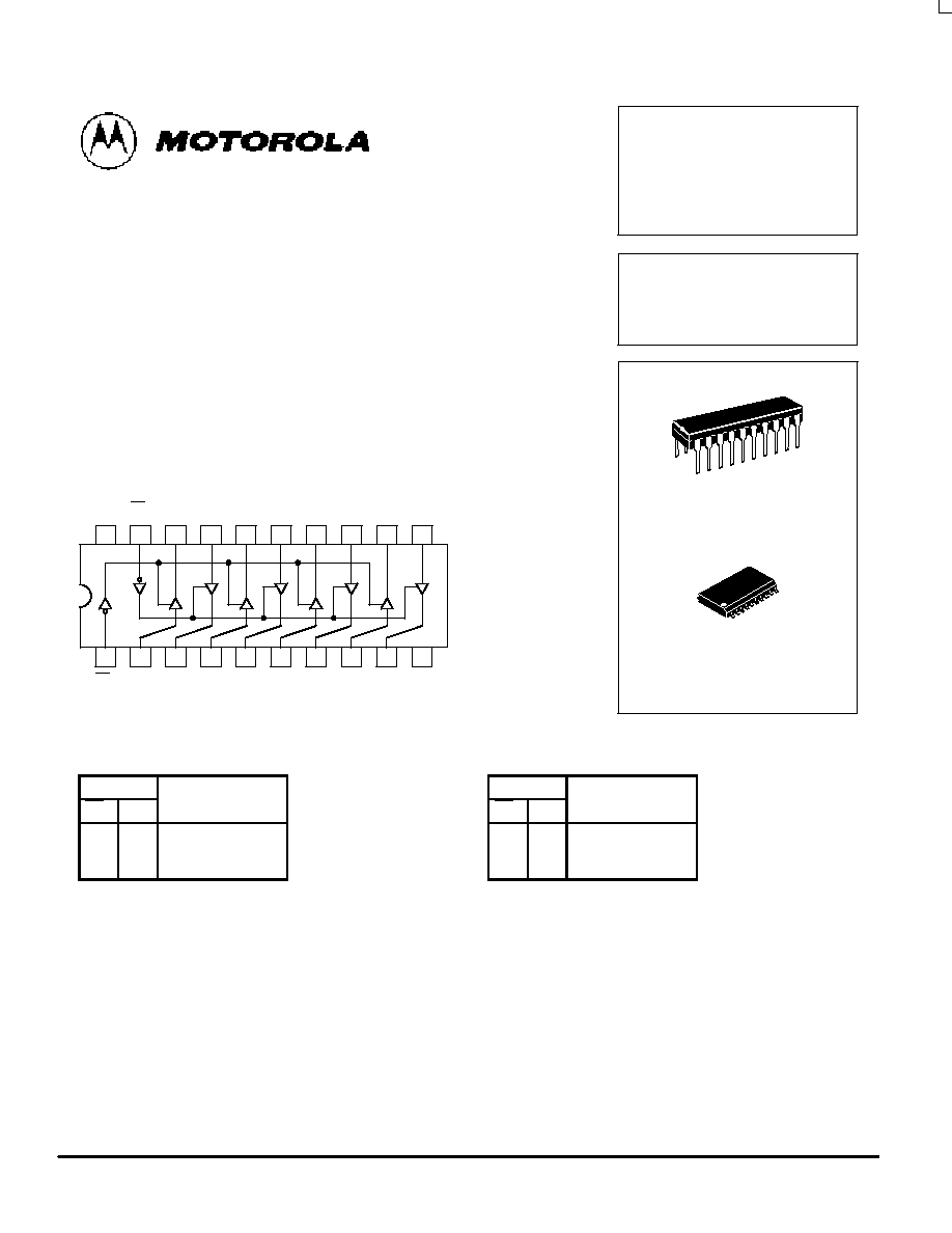
Octal Buffer/Line Driver
with 3 State Outputs
The MC74AC244/74ACT244 is an octal buffer and line driver designed to be
employed as a memory address driver, clock driver and bus oriented transmitter/
receiver which provides improved PC board density.
·
3-State Outputs Drive Bus Lines or Buffer Memory Address Registers
·
Outputs Source/Sink 24 mA
·
ACT244 Has TTL Compatible Inputs
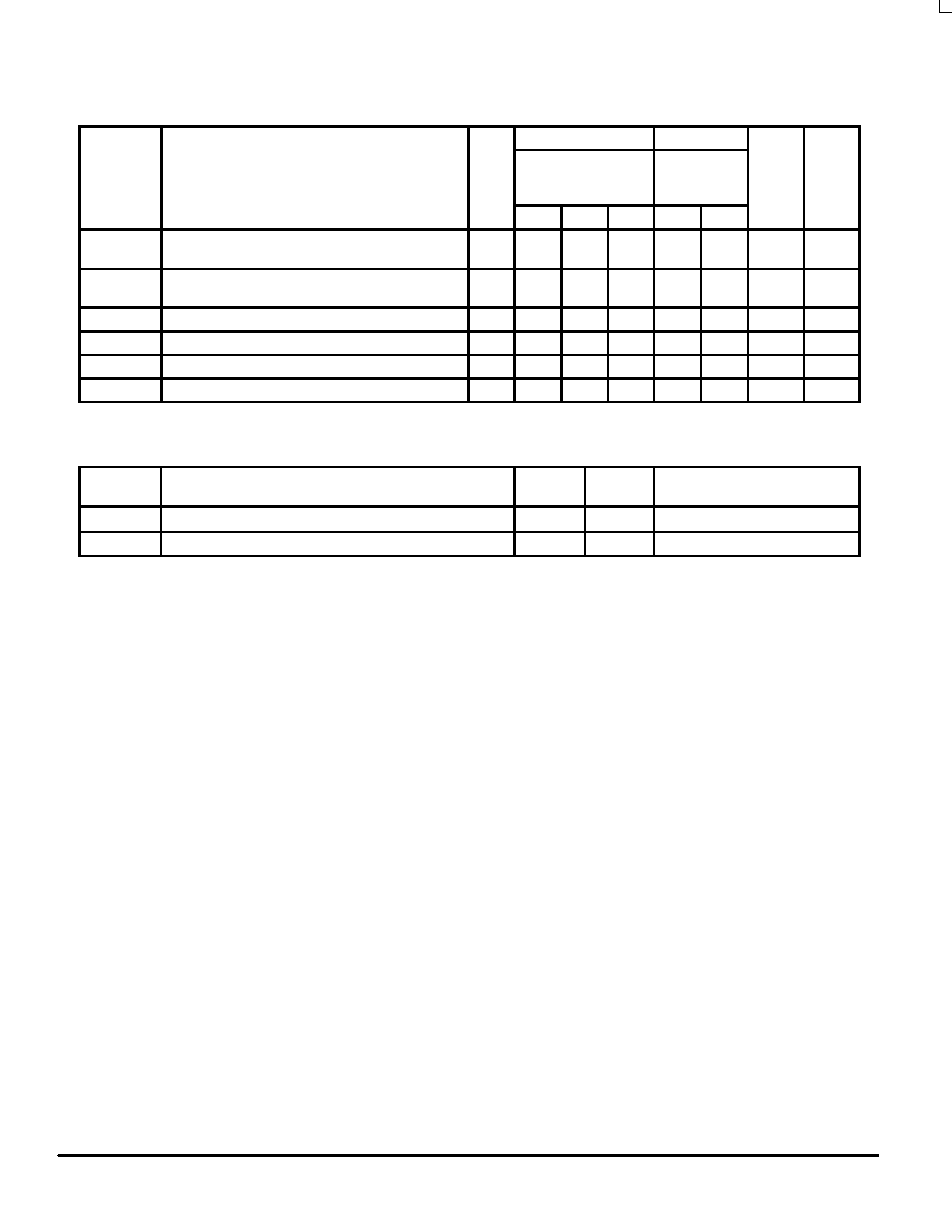
19
20
18
17
16
15
14
2
1
3
4
5
6
7
VCC
13
8
12
9
11
10
OE2
OE1
GND
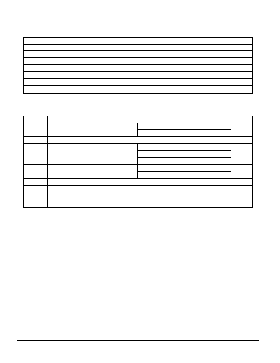
TRUTH TABLE
Inputs
Outputs
OE1
D
(Pins 12, 14, 16, 18)
L
L
L
L
H
H
H
X
Z
H = HIGH Voltage Level
L = LOW Voltage Level
X = Immaterial
Z = High Impedance
TRUTH TABLE
Inputs
Outputs
OE2
D
(Pins 3, 5, 7, 9)
L
L
L
L
H
H
H
X
Z
H = HIGH Voltage Level
L = LOW Voltage Level
X = Immaterial
Z = High Impedance
MC74AC244
MC74ACT244
OCTAL BUFFER/LINE
DRIVER WITH
3-STATE OUTPUTS
N SUFFIX
CASE 738-03
PLASTIC
DW SUFFIX
CASE 751D-04
PLASTIC
MC74AC244 MC74ACT244
5-2
FACT DATA
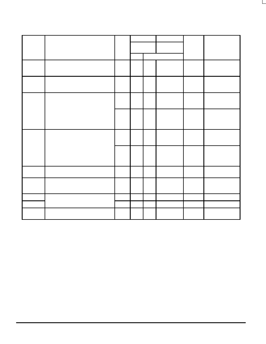
MAXIMUM RATINGS*
Symbol
Parameter
Value
Unit
VCC
DC Supply Voltage (Referenced to GND)
0.5 to +7.0
V
Vin
DC Input Voltage (Referenced to GND)
0.5 to VCC +0.5
V
Vout
DC Output Voltage (Referenced to GND)
0.5 to VCC +0.5
V
Iin
DC Input Current, per Pin
±
20
mA
Iout
DC Output Sink/Source Current, per Pin
±
50
mA
ICC
DC VCC or GND Current per Output Pin
±
50
mA
Tstg
Storage Temperature
65 to +150
°
C
* Maximum Ratings are those values beyond which damage to the device may occur. Functional operation should be restricted to the Recommended
Operating Conditions.
RECOMMENDED OPERATING CONDITIONS
Symbol
Parameter
Min
Typ
Max
Unit
VCC
Supply Voltage
AC
2.0
5.0
6.0
V
VCC
Supply Voltage
ACT
4.5
5.0
5.5
V
Vin, Vout
DC Input Voltage, Output Voltage (Ref. to GND)
0
VCC
V
tr, tf
Input Rise and Fall Time (Note 1)
AC Devices except Schmitt Inputs
VCC @ 3.0 V
150
tr, tf
Input Rise and Fall Time (Note 1)
AC Devices except Schmitt Inputs
VCC @ 4.5 V
40
ns/V
r, tf
AC Devices except Schmitt Inputs
VCC @ 5.5 V
25
tr, tf
Input Rise and Fall Time (Note 2)
ACT Devices except Schmitt Inputs
VCC @ 4.5 V
10
ns/V
tr, tf
Input Rise and Fall Time (Note 2)
ACT Devices except Schmitt Inputs
VCC @ 5.5 V
8.0
ns/V
TJ
Junction Temperature (PDIP)
140
°
C
TA
Operating Ambient Temperature Range
40
25
85
°
C
IOH
Output Current -- High
24
mA
IOL
Output Current -- Low
24
mA
1. Vin from 30% to 70% VCC; see individual Data Sheets for devices that differ from the typical input rise and fall times.
2. Vin from 0.8 V to 2.0 V; see individual Data Sheets for devices that differ from the typical input rise and fall times.
MC74AC244 MC74ACT244
5-3
FACT DATA
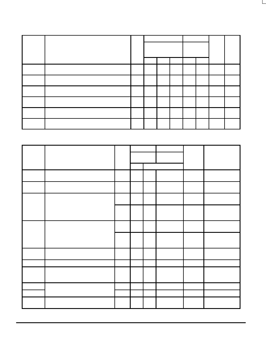
DC CHARACTERISTICS
Symbol
Parameter
VCC
(V)
74AC
74AC
Unit
Conditions
Symbol
Parameter
VCC
(V)
TA = +25
°
C
TA =
40
°
C to +85
°
C
Unit
Conditions
Typ
Guaranteed Limits
VIH
Minimum High Level
Input Voltage
3.0
1.5
2.1
2.1
VOUT = 0.1 V
Input Voltage
4.5
2.25
3.15
3.15
V
or VCC 0.1 V
5.5
2.75
3.85
3.85
VIL
Maximum Low Level
Input Voltage
3.0
1.5
0.9
0.9
VOUT = 0.1 V
Input Voltage
4.5
2.25
1.35
1.35
V
or VCC 0.1 V
5.5
2.75
1.65
1.65
VOH
Minimum High Level
Output Voltage
3.0
2.99
2.9
2.9
IOUT = 50
µ
A
Output Voltage
4.5
4.49
4.4
4.4
V
5.5
5.49
5.4
5.4
V
*VIN = VIL or VIH
3.0
2.56
2.46
V
12 mA
4.5
3.86
3.76
V
IOH
24 mA
5.5
4.86
4.76
24 mA
VOL
Maximum Low Level
Output Voltage
3.0
0.002
0.1
0.1
IOUT = 50
µ
A
Output Voltage
4.5
0.001
0.1
0.1
V
5.5
0.001
0.1
0.1
V
*VIN = VIL or VIH
3.0
0.36
0.44
V
12 mA
4.5
0.36
0.44
V
IOL
24 mA
5.5
0.36
0.44
24 mA
IIN
Maximum Input
Leakage Current
5.5
±
0.1
±
1.0
µ
A
VI = VCC, GND
Leakage Current
5.5
±
0.1
±
1.0
µ
A
VI = VCC, GND
IOZ
Maximum
3-State
Current
VI (OE) = VIL, VIH
3-State
Current
5.5
±
0.5
±
5.0
µ
A
VI = VCC, GND
Current
VO = VCC, GND
IOLD
Minimum Dynamic
Output Current
5.5
75
mA
VOLD = 1.65 V Max
IOHD
Output Current
5.5
75
mA
VOHD = 3.85 V Min
ICC
Maximum Quiescent
Supply Current
5.5
8.0
80
µ
A
VIN = VCC or GND
Supply Current
5.5
8.0
80
µ
A
VIN = VCC or GND
* All outputs loaded; thresholds on input associated with output under test.
Maximum test duration 2.0 ms, one output loaded at a time.
Note: IIN and ICC @ 3.0 V are guaranteed to be less than or equal to the respective limit @ 5.5 V VCC.
MC74AC244 MC74ACT244
5-4
FACT DATA
AC CHARACTERISTICS (For Figures and Waveforms -- See Section 3)
Symbol
Parameter
VCC*
(V)
74AC
74AC
Unit
Fig.
No.
Symbol
Parameter
VCC*
(V)
TA = +25
°
C
CL = 50 pF
TA = 40
°
C
to +85
°
C
CL = 50 pF
Unit
Fig.
No.
Min
Typ
Max
Min
Max
tPLH
Propagation Delay
3.3
2.0
6.5
9.0
1.5
10.0
ns
3-5
tPLH
Data to Output
5.0
1.5
5.0
7.0
1.0
7.5
ns
3-5
tPHL
Propagation Delay
3.3
2.0
6.5
9.0
2.0
10.0
ns
3-5
tPHL
Data to Output
5.0
1.5
5.0
7.0
1.0
7.5
ns
3-5
tPZH
Output Enable Time
3.3
2.0
6.0
10.5
1.5
11.0
ns
3-7
tPZH
Output Enable Time
5.0
1.5
5.0
7.0
1.5
8.0
ns
3-7
tPZL
Output Enable Time
3.3
2.5
7.5
10.0
2.0
11.0
ns
3-8
tPZL
Output Enable Time
5.0
1.5
5.5
8.0
1.5
8.5
ns
3-8
tPHZ
Output Disable Time
3.3
3.0
7.0
10.0
1.5
10.5
ns
3-7
tPHZ
Output Disable Time
5.0
2.5
6.5
9.0
1.0
9.5
ns
3-7
tPLZ
Output Disable Time
3.3
2.5
7.5
10.5
2.5
11.5
ns
3-8
tPLZ
Output Disable Time
5.0
2.0
6.5
9.0
2.0
9.5
ns
3-8
* Voltage Range 3.3 V is 3.3 V
±
0.3 V.
Voltage Range 5.0 V is 5.0 V
±
0.5 V.
DC CHARACTERISTICS
Symbol
Parameter
VCC
(V)
74ACT
74ACT
Unit
Conditions
Symbol
Parameter
VCC
(V)
TA = +25
°
C
TA =
40
°
C to +85
°
C
Unit
Conditions
Typ
Guaranteed Limits
VIH
Minimum High Level
Input Voltage
4.5
1.5
2.0
2.0
V
VOUT = 0.1 V
Input Voltage
5.5
1.5
2.0
2.0
V
or VCC 0.1 V
VIL
Maximum Low Level
Input Voltage
4.5
1.5
0.8
0.8
V
VOUT = 0.1 V
Input Voltage
5.5
1.5
0.8
0.8
V
or VCC 0.1 V
VOH
Minimum High Level
Output Voltage
4.5
4.49
4.4
4.4
V
IOUT = 50
µ
A
Output Voltage
5.5
5.49
5.4
5.4
V
*VIN = VIL or VIH
4.5
3.86
3.76
V
IOH
24 mA
5.5
4.86
4.76
IOH
24 mA
VOL
Maximum Low Level
Output Voltage
4.5
0.001
0.1
0.1
V
IOUT = 50
µ
A
Output Voltage
5.5
0.001
0.1
0.1
V
*VIN = VIL or VIH
4.5
0.36
0.44
V
IOL
24 mA
5.5
0.36
0.44
IOL
24 mA
IIN
Maximum Input
Leakage Current
5.5
±
0.1
±
1.0
µ
A
VI = VCC, GND
Leakage Current
5.5
±
0.1
±
1.0
µ
A
VI = VCC, GND
ICCT
Additional Max. ICC/Input
5.5
0.6
1.5
mA
VI = VCC 2.1 V
IOZ
Maximum
3-State
Current
VI (OE) = VIL, VIH
3-State
Current
5.5
±
0.5
±
5.0
µ
A
VI = VCC, GND
Current
VO = VCC, GND
IOLD
Minimum Dynamic
Output Current
5.5
75
mA
VOLD = 1.65 V Max
IOHD
Output Current
5.5
75
mA
VOHD = 3.85 V Min
ICC
Maximum Quiescent
Supply Current
5.5
8.0
80
µ
A
VIN = VCC or GND
Supply Current
5.5
8.0
80
µ
A
VIN = VCC or GND
* All outputs loaded; thresholds on input associated with output under test.
Maximum test duration 2.0 ms, one output loaded at a time.
MC74AC244 MC74ACT244
5-5
FACT DATA
AC CHARACTERISTICS (For Figures and Waveforms -- See Section 3)
Symbol
Parameter
VCC*
(V)
74ACT
74ACT
Unit
Fig.
No.
Symbol
Parameter
VCC*
(V)
TA = +25
°
C
CL = 50 pF
TA = 40
°
C
to +85
°
C
CL = 50 pF
Unit
Fig.
No.
Min
Typ
Max
Min
Max
tPLH
Propagation Delay
Data to Output
5.0
2.0
6.5
9.0
1.5
10.0
ns
3-5
tPLH
Data to Output
5.0
2.0
6.5
9.0
1.5
10.0
ns
3-5
tPHL
Propagation Delay
Data to Output
5.0
2.0
7.0
9.0
1.5
10.0
ns
3-5
tPHL
Data to Output
5.0
2.0
7.0
9.0
1.5
10.0
ns
3-5
tPZH
Output Enable Time
5.0
1.5
6.0
8.5
1.0
9.5
ns
3-7
tPZL
Output Enable Time
5.0
2.0
7.0
9.5
1.5
10.5
ns
3-8
tPHZ
Output Disable Time
5.0
2.0
7.0
9.5
1.5
10.5
ns
3-7
tPLZ
Output Disable Time
5.0
2.5
7.5
10.0
2.0
10.5
ns
3-8
* Voltage Range 5.0 V is 5.0 V
±
0.5 V.
CAPACITANCE
Symbol
Parameter
Value
Typ
Unit
Test Conditions
CIN
Input Capacitance
4.5
pF
VCC = 5.0 V
CPD
Power Dissipation Capacitance
45
pF
VCC = 5.0 V
MC74AC244 MC74ACT244
5-6
FACT DATA
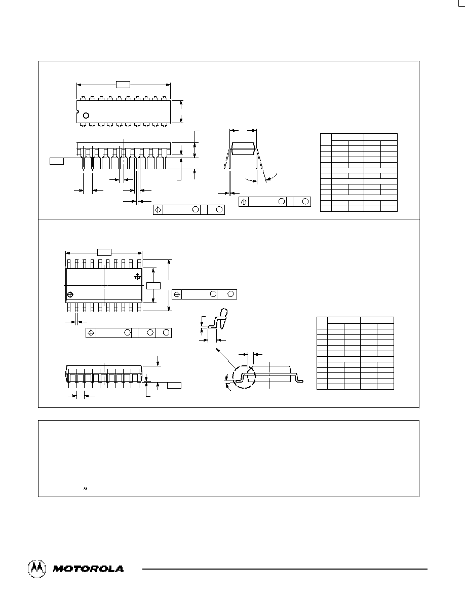
OUTLINE DIMENSIONS
N SUFFIX
PLASTIC DIP PACKAGE
CASE 73803
ISSUE E
DW SUFFIX
PLASTIC SOIC PACKAGE
CASE 751D04
ISSUE E
NOTES:
1. DIMENSIONING AND TOLERANCING PER
ANSI Y14.5M, 1982.
2. CONTROLLING DIMENSION: MILLIMETER.
3. DIMENSIONS A AND B DO NOT INCLUDE
MOLD PROTRUSION.
4. MAXIMUM MOLD PROTRUSION 0.150
(0.006) PER SIDE.
5. DIMENSION D DOES NOT INCLUDE
DAMBAR PROTRUSION. ALLOWABLE
DAMBAR PROTRUSION SHALL BE 0.13
(0.005) TOTAL IN EXCESS OF D
DIMENSION AT MAXIMUM MATERIAL
CONDITION.
A
B
20
1
11
10
S
A
M
0.010 (0.25)
B
S
T
D
20X
M
B
M
0.010 (0.25)
P
10X
J
F
G
18X
K
C
T
SEATING
PLANE
M
R
X 45
_
DIM
MIN
MAX
MIN
MAX
INCHES
MILLIMETERS
A
12.65
12.95
0.499
0.510
B
7.40
7.60
0.292
0.299
C
2.35
2.65
0.093
0.104
D
0.35
0.49
0.014
0.019
F
0.50
0.90
0.020
0.035
G
1.27 BSC
0.050 BSC
J
0.25
0.32
0.010
0.012
K
0.10
0.25
0.004
0.009
M
0
7
0
7
P
10.05
10.55
0.395
0.415
R
0.25
0.75
0.010
0.029
_
_
_
_
NOTES:
1. DIMENSIONING AND TOLERANCING PER
ANSI Y14.5M, 1982.
2. CONTROLLING DIMENSION: INCH.
3. DIMENSION L TO CENTER OF LEAD WHEN
FORMED PARALLEL.
4. DIMENSION B DOES NOT INCLUDE MOLD
FLASH.
M
L
J
20 PL
M
B
M
0.25 (0.010)
T
DIM
MIN
MAX
MIN
MAX
MILLIMETERS
INCHES
A
25.66
27.17
1.010
1.070
B
6.10
6.60
0.240
0.260
C
3.81
4.57
0.150
0.180
D
0.39
0.55
0.015
0.022
G
2.54 BSC
0.100 BSC
J
0.21
0.38
0.008
0.015
K
2.80
3.55
0.110
0.140
L
7.62 BSC
0.300 BSC
M
0
15
0
15
N
0.51
1.01
0.020
0.040
_
_
_
_
E
1.27
1.77
0.050
0.070
1
11
10
20
A
SEATING
PLANE
K
N
F
G
D
20 PL
T
M
A
M
0.25 (0.010)
T
E
B
C
F
1.27 BSC
0.050 BSC
How to reach us:
USA/EUROPE: Motorola Literature Distribution;
JAPAN: Nippon Motorola Ltd.; TatsumiSPDJLDC, Toshikatsu Otsuki,
P.O. Box 20912; Phoenix, Arizona 85036. 18004412447
6F SeibuButsuryuCenter, 3142 Tatsumi KotoKu, Tokyo 135, Japan. 0335218315
MFAX: RMFAX0@email.sps.mot.com TOUCHTONE (602) 2446609
HONG KONG: Motorola Semiconductors H.K. Ltd.; 8B Tai Ping Industrial Park,
INTERNET: http://DesignNET.com
51 Ting Kok Road, Tai Po, N.T., Hong Kong. 85226629298
Motorola reserves the right to make changes without further notice to any products herein. Motorola makes no warranty, representation or guarantee regarding
the suitability of its products for any particular purpose, nor does Motorola assume any liability arising out of the application or use of any product or circuit, and
specifically disclaims any and all liability, including without limitation consequential or incidental damages. "Typical" parameters can and do vary in different
applications. All operating parameters, including "Typicals" must be validated for each customer application by customer's technical experts. Motorola does
not convey any license under its patent rights nor the rights of others. Motorola products are not designed, intended, or authorized for use as components in
systems intended for surgical implant into the body, or other applications intended to support or sustain life, or for any other application in which the failure of
the Motorola product could create a situation where personal injury or death may occur. Should Buyer purchase or use Motorola products for any such
unintended or unauthorized application, Buyer shall indemnify and hold Motorola and its officers, employees, subsidiaries, affiliates, and distributors harmless
against all claims, costs, damages, and expenses, and reasonable attorney fees arising out of, directly or indirectly, any claim of personal injury or death
associated with such unintended or unauthorized use, even if such claim alleges that Motorola was negligent regarding the design or manufacture of the part.
Motorola and
are registered trademarks of Motorola, Inc. Motorola, Inc. is an Equal Opportunity/Affirmative Action Employer.
MC74AC244/D
*MC74AC244/D*